EP2742595B1 - Verfahren zum erzeugen eines digitalen signals - Google Patents
Verfahren zum erzeugen eines digitalen signals Download PDFInfo
- Publication number
- EP2742595B1 EP2742595B1 EP12753426.1A EP12753426A EP2742595B1 EP 2742595 B1 EP2742595 B1 EP 2742595B1 EP 12753426 A EP12753426 A EP 12753426A EP 2742595 B1 EP2742595 B1 EP 2742595B1
- Authority
- EP
- European Patent Office
- Prior art keywords
- weighting
- bit
- pulse width
- width modulation
- period
- Prior art date
- Legal status (The legal status is an assumption and is not a legal conclusion. Google has not performed a legal analysis and makes no representation as to the accuracy of the status listed.)
- Active
Links
Images

Classifications
-
- H—ELECTRICITY
- H04—ELECTRIC COMMUNICATION TECHNIQUE
- H04L—TRANSMISSION OF DIGITAL INFORMATION, e.g. TELEGRAPHIC COMMUNICATION
- H04L25/00—Baseband systems
- H04L25/38—Synchronous or start-stop systems, e.g. for Baudot code
- H04L25/40—Transmitting circuits; Receiving circuits
- H04L25/49—Transmitting circuits; Receiving circuits using code conversion at the transmitter; using predistortion; using insertion of idle bits for obtaining a desired frequency spectrum; using three or more amplitude levels ; Baseband coding techniques specific to data transmission systems
- H04L25/4902—Pulse width modulation; Pulse position modulation
-
- H—ELECTRICITY
- H03—ELECTRONIC CIRCUITRY
- H03M—CODING; DECODING; CODE CONVERSION IN GENERAL
- H03M3/00—Conversion of analogue values to or from differential modulation
- H03M3/30—Delta-sigma modulation
- H03M3/458—Analogue/digital converters using delta-sigma modulation as an intermediate step
- H03M3/462—Details relating to the decimation process
-
- H—ELECTRICITY
- H04—ELECTRIC COMMUNICATION TECHNIQUE
- H04B—TRANSMISSION
- H04B1/00—Details of transmission systems, not covered by a single one of groups H04B3/00 - H04B13/00; Details of transmission systems not characterised by the medium used for transmission
- H04B1/38—Transceivers, i.e. devices in which transmitter and receiver form a structural unit and in which at least one part is used for functions of transmitting and receiving
- H04B1/40—Circuits
-
- H—ELECTRICITY
- H02—GENERATION; CONVERSION OR DISTRIBUTION OF ELECTRIC POWER
- H02M—APPARATUS FOR CONVERSION BETWEEN AC AND AC, BETWEEN AC AND DC, OR BETWEEN DC AND DC, AND FOR USE WITH MAINS OR SIMILAR POWER SUPPLY SYSTEMS; CONVERSION OF DC OR AC INPUT POWER INTO SURGE OUTPUT POWER; CONTROL OR REGULATION THEREOF
- H02M5/00—Conversion of AC power input into AC power output, e.g. for change of voltage, for change of frequency, for change of number of phases
- H02M5/40—Conversion of AC power input into AC power output, e.g. for change of voltage, for change of frequency, for change of number of phases with intermediate conversion into DC
- H02M5/42—Conversion of AC power input into AC power output, e.g. for change of voltage, for change of frequency, for change of number of phases with intermediate conversion into DC by static converters
- H02M5/44—Conversion of AC power input into AC power output, e.g. for change of voltage, for change of frequency, for change of number of phases with intermediate conversion into DC by static converters using discharge tubes or semiconductor devices to convert the intermediate DC into AC
- H02M5/443—Conversion of AC power input into AC power output, e.g. for change of voltage, for change of frequency, for change of number of phases with intermediate conversion into DC by static converters using discharge tubes or semiconductor devices to convert the intermediate DC into AC using devices of a thyratron or thyristor type requiring extinguishing means
- H02M5/45—Conversion of AC power input into AC power output, e.g. for change of voltage, for change of frequency, for change of number of phases with intermediate conversion into DC by static converters using discharge tubes or semiconductor devices to convert the intermediate DC into AC using devices of a thyratron or thyristor type requiring extinguishing means using semiconductor devices only
Definitions
- the invention relates to a method for generating a digital signal from an analog signal generated by means of a frequency converter and a frequency converter for carrying out the method.
- Frequency converters typically generate pulse-width-modulated signals for controlling electric motors, for example in the form of a (phase) voltage, wherein the phase voltage in turn causes a phase current.
- phase voltage in turn causes a phase current.
- frequency converters which reduce the phase current in the context of control, the quality of the signal measurement or signal feedback is of great importance.
- the signals to be measured are usually recorded by means of suitable sensors, filtered analogously and then sampled and digitized by means of conventional analog-to-digital converters.
- the generally sawtooth-shaped phase current as one of the relevant signals is usually sampled synchronously in the middle of a respective period of the pulse width modulation. However, if not exactly centered, an offset measurement error can be caused.
- the US 2007/0108953 A1 discloses a switching power supply with a control circuit comprising an A / D converter for digitizing the analog output signal of the switched mode power supply.
- the US 5,940,019 A shows an A / D converter with a delta-sigma modulator whose output bit stream is multiplied by a data conversion value, the data conversion value determining a gain. The values thus obtained are then data rate reduced by means of a decimation filter to produce a digital output signal.
- the invention has for its object to provide a method for generating a digital signal from a generated by means of a frequency converter based on a pulse width modulation analog signal and a frequency converter for performing the method available that are simple and inexpensive to implement and in particular an interference-proof and enable reliable digitization.
- the invention achieves this object by a method according to claim 1 and a frequency converter according to claim 5.
- the method is used to generate at least one digital or digitized signal from an analog signal generated by means of a frequency converter on the basis of a pulse width modulation, for example a phase current and / or a phase voltage, which serves to drive an electric motor, wherein the digital signal, in particular in digital representation , an average value of the analog signal over a period of the pulse width modulation corresponds.
- the digital signal is used in particular for controlling the analog signal, for example in a servo inverter.
- a continuous bit stream is generated with a predetermined, in particular constant, bit repetition duration as a function of the analog signal, in particular by means of a sigma-delta modulator.
- the following steps are performed: multiplying a respective bit of the bitstream by an associated weighting coefficient to produce a respective bit weighting coefficient product and summing all bitstreams; Rating coefficient products over the time interval, the sum over the time interval representing the digital signal.
- the above steps are repeated continuously, for example, for each period or every nth period of the pulse width modulation, with n ⁇ 2.
- a digital representation of a signal or a digital signal is understood to mean a sequence of time- and amplitude-discretely digitized sampled values, which on the one hand have a delimited and stepped value supply and, moreover, are defined in the temporal sequence only at specific periodic time points or one change in the sampled value demonstrate.
- the signal in digital representation is formed from an associated analog signal, which describes the time-continuous course of a physical quantity, by quantization and sampling, which takes place at defined times.
- a digital signal in a binary representation be transferred.
- the weighting coefficients are generated by superimposing weighting coefficients of a weighting function, wherein a midpoint of a respective weighting function is within a period of the pulse width modulation, a respective weighting function corresponds to a digital filter function, adjacent one
- Weighting functions are shifted in time by one or a multiple of the Bitwiederholdauer each other and each weighting function has a predetermined number of weighting coefficients.
- the time interval has a duration that is longer than a period of the pulse width modulation by a number of bit repetition durations, the number of bit repetition durations corresponding to the number of weighting coefficients.
- the time interval is arranged centrically to a period of the pulse width modulation.
- the digital filter function is a sinc filter function.
- the frequency converter in particular in the form of a servo-inverter, is designed to carry out the above-mentioned method and comprises: a sigma-delta modulator for generating the bitstream, a memory storing the weighting coefficients, a multiplier designed to multiplying a respective bit of the bitstream by an associated weighting coefficient, and a summer configured to sum the respective bit weighting coefficient products.
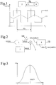
- Fig. 1 shows conventionally by means of a frequency converter 5 based on a pulse width modulation generated or effected analog signals in the form of a substantially rectangular, pulse width modulated phase voltage UA with a variable duty cycle and an associated, sage leopardförmigen phase current IA, as in a conventional pulse width modulation based control of an electric motor 6 by the frequency converter 5 arise.
- the signals UA and / or IA are continuously digitized in accordance with the invention in a time-discrete and amplitude-discrete manner, the digital or digitized signal corresponding to an average value of the analog signal UA or IA over a period PD of the pulse width modulation.
- a period can be, for example, about 0.25 ms and changed as needed.
- the bit repetition BW can, for example 0.25 ⁇ s, which corresponds to a bit repetition frequency of 4 MHz.
- a time interval ZI (see Fig. 4 ), which has a duration which is at least as long as the period duration PD of the pulse width modulation, all bits BS (i) of the bit stream are combined with an associated evaluation coefficient BK (i) stored in a memory 2 for generating a respective bit weighting coefficient.
- Product multiplied by a multiplier 3 The bit weighting coefficient products thus generated are summed by means of a summer 4, the sum representing the digital signal DS over the time interval ZI.
- Fig. 3 shows a weighting function GF of a conventional digital sinc 3 filter with an oversampling ratio of 128 with a total of 384 weighting coefficients GK (i).
- Such filters are conventionally used at the output of sigma-delta modulators for data rate reduction.
- Fig. 4 shows based on the in Fig. 3 shown, single weighting function GF a plurality of adjacent weighting functions GF, which are shifted by P steps to each other.
- a single step corresponds to the bit repetition duration BW of the sigma-delta modulator 1, as already explained above, so that the weighting functions GF are shifted from each other by P bit repetition durations BW in the time domain or over time.
- the time interval ZI thus has a duration that is increased by the number of weighting coefficients of the in Fig. 2 shown sinc 3 filters multiplied by the bit repetition BW is longer than the period PD of the pulse width modulation.
- the time interval ZI is arranged centric to the period of the pulse width modulation.
- the weighting coefficients BK (i) are now generated by superimposing the weighting coefficients GK (i) of the weighting function GF whose center lies within the period of the pulse width modulation. These are the weighting functions marked with the numbers 0 to 3.
- the average is formed over a plurality of fully digitized samples within the period.
- appropriately parallelized hardware is to be provided, which provides these samples with a suitable decimated sampling rate with the required temporal resolution and word width.
- the integral of the evaluation or weighting function associated decimation filter is used according to the invention, the coefficients required for this purpose are precalculated and stored in a memory.
- the integrated evaluation function further has the property of being flat in the middle range, see Fig. 4 . This property can be used, for example, to minimize the memory requirements for the coefficients, since only the rising and falling edges are to be stored.
- this property facilitates adaptation to a variable period.
- the period of the pulse width modulated Signals is a simple adaptation of the method according to the invention, for example, possible in that the coefficients GK (i) are adjusted accordingly. For example, if based on the representation in Fig. 4 the period PD is extended, only extends the duration of the plateau with constant coefficients BK (i), the edges remain unchanged.
- a superimposition or integration of the weighting or evaluation function takes place, unlike the conventional decimated samples.
- the application of the superimposed weighting functions takes place from a memory.
- An exact adaptation of the superimposed weighting function to the period of the pulse width modulation is easily possible. Almost arbitrary functions can be used as weighting functions, so that a multiplicity of associated filter functions can be used.
- Sinc filters are no longer needed, so significantly less hardware resources are consumed.
- the weighting coefficients can be used simultaneously for voltage and current.
- the invention thus enables a simple and cost-effective to be implemented digitization of inverter signals, while at the same time an interference-proof and reliable digitization is ensured.
Landscapes
- Engineering & Computer Science (AREA)
- Computer Networks & Wireless Communication (AREA)
- Signal Processing (AREA)
- Theoretical Computer Science (AREA)
- Physics & Mathematics (AREA)
- Spectroscopy & Molecular Physics (AREA)
- Compression, Expansion, Code Conversion, And Decoders (AREA)
- Analogue/Digital Conversion (AREA)
Description
- Die Erfindung betrifft ein Verfahren zum Erzeugen eines digitalen Signals aus einem mittels eines Frequenzumrichters erzeugten analogen Signal und einen Frequenzumrichter zur Durchführung des Verfahrens.
- Frequenzumrichter erzeugen zur Ansteuerung von Elektromotoren typisch pulsweitenmodulierte Signale, beispielsweise in Form einer (Phasen-)Spannung, wobei die Phasenspannung wiederum einen Phasenstrom bewirkt. Bei Frequenzumrichtern, die den Phasenstrom im Kontext einer Regelung zurückführen, ist die Qualität der Signalmessung bzw. Signalrückführung von hoher Bedeutung.
- Die zu messenden Signale werden hierzu üblicherweise mittels geeigneter Sensoren aufgenommen, analog gefiltert und anschließend mittels herkömmlicher Analog-Digital-Wandler abgetastet und digitalisiert.
- Der im Allgemeinen sägezahnförmige Phasenstrom als eines der relevanten Signale wird üblicherweise synchron in der Mitte einer jeweiligen Periode der Pulsweitenmodulation abgetastet. Bei nicht exakt mittiger Abtastung kann jedoch ein Offset-Messfehler verursacht werden.
- Durch Mittelwertbildung über eine Periodendauer der Pulsweitenmodulation lassen sich die oben genannten Störeffekte reduzieren. Zur Mittelwertbildung wird herkömmlich eine Mehrzahl von digitalen Messwerten über eine Periodendauer der Pulsweitenmodulation gewonnen und anschließend ein Mittelwert über die gewonnenen Messwerte berechnet. Ein Verfahren, bei dem eine solche Mittelwertbildung durchgeführt wird, ist in der
DE 10 2007 032 484 A1 beschrieben. - Die
US 2007/0108953 A1 offenbart ein Schaltnetzteil mit einer Regelungsschaltung, die einen A/D-Wandler zur Digitalisierung des analogen Ausgangssignals des Schaltnetzteils umfasst. - Die
US 5,940,019 A zeigt einen A/D-Wandler mit einem Delta-Sigma-Modulator, dessen Ausgangsbitstrom mit einem Datenwandlungswert multipliziert wird, wobei der Datenwandlungswert eine Verstärkung bestimmt. Die derart gewonnenen Werte werden anschließend mittels eines Dezimierungsfilters datenratenreduziert, um ein digitales Ausgangssignal zu erzeugen. - Der Erfindung liegt die Aufgabe zugrunde, ein Verfahren zum Erzeugen eines digitalen Signals aus einem mittels eines Frequenzumrichters auf Basis einer Pulsweitenmodulation erzeugten analogen Signal und einen Frequenzumrichter zur Durchführung des Verfahrens zur Verfügung zu stellen, die einfach und kostengünstig zu implementieren sind und die insbesondere eine störsichere und zuverlässige Digitalisierung ermöglichen.
- Die Erfindung löst diese Aufgabe durch ein Verfahren nach Anspruch 1 und einen Frequenzumrichter nach Anspruch 5.
- Bevorzugte Ausführungsformen sind Gegenstand der Unteransprüche, deren Wortlaut hiermit durch Bezugnahme zum Inhalt der Beschreibung gemacht wird.
- Das Verfahren dient zum Erzeugen mindestens eines digitalen bzw. digitalisierten Signals aus einem mittels eines Frequenzumrichters auf Basis einer Pulsweitenmodulation erzeugten analogen Signal, beispielsweise eines Phasenstroms und/oder einer Phasenspannung, das zur Ansteuerung eines Elektromotors dient, wobei das digitale Signal, insbesondere in digitaler Darstellung, einem Mittelwert des analogen Signals über eine Periodendauer der Pulsweitenmodulation entspricht. Das digitale Signal dient insbesondere zur Regelung des analogen Signals, beispielsweise in einem Servo-Umrichter. Bei dem Verfahren wird ein fortlaufender Bitstrom mit einer vorgegebenen, insbesondere konstanten, Bitwiederholdauer in Abhängigkeit von dem analogen Signal erzeugt, insbesondere mittels eines Sigma-Delta-Modulators. Während eines jeweiligen Zeitintervalls, welches eine Dauer aufweist, die mindestens so groß ist wie die Periodendauer der Pulsweitenmodulation, werden folgende Schritte durchgeführt: Multiplizieren eines jeweiligen Bits des Bitstroms mit einem zugehörigen Bewertungskoeffizienten zum Erzeugen eines jeweiligen Bit-Bewertungskoeffizienten-Produkts und Summieren sämtlicher Bit-Bewertungskoeffizienten-Produkte über das Zeitintervall, wobei die Summe über das Zeitintervall das digitale Signal darstellt. Die oben genannten Schritte werden fortlaufend wiederholt, beispielsweise für jede Periode oder jede n-te Periode der Pulsweitenmodulation, mit n ≥ 2.
- Unter einer digitalen Darstellung eines Signals bzw. einem digitalen Signal wird eine Folge von zeit- und amplitudendiskret digitalisierten Abtastwerten verstanden, die einerseits einen abgegrenzten und gestuften Wertvorrat aufweisen und zudem in der zeitlichen Abfolge nur zu bestimmten periodischen Zeitpunkten definiert sind bzw. eine Veränderung im Abtastwert zeigen. Das Signal in digitaler Darstellung wird aus einem zugehörigen analogen Signal, welches den zeitlich kontinuierlichen Verlauf einer physikalischen Größe beschreibt, durch Quantisierung und Abtastung, welche zu definierten Zeitpunkten erfolgt, gebildet. Durch eine entsprechende Codierung kann ein Digitalsignal in eine binäre Darstellung übergeführt werden. Im Übrigen sei auch auf die umfangreiche Fachliteratur verwiesen.
- Die Bewertungskoeffizienten werden durch Überlagern von Gewichtungskoeffizienten einer Gewichtungsfunktion erzeugt, wobei ein Mittelpunkt einer jeweiligen Gewichtungsfunktion innerhalb einer Periode der Pulsweitenmodulation liegt, eine jeweilige Gewichtungsfunktion einer digitalen Filterfunktion entspricht, benachbarte
- Gewichtungsfunktionen zeitlich um eine oder eine Vielfache der Bitwiederholdauer zueinander verschoben sind und eine jeweilige Gewichtsfunktion eine vorgegebene Anzahl von Gewichtungskoeffizienten aufweist. Bevorzugt weist das Zeitintervall eine Dauer auf, die um eine Anzahl von Bitwiederholdauern länger ist als eine Periodendauer der Pulsweitenmodulation, wobei die Anzahl von Bitwiederholdauern der Anzahl von Gewichtungskoeffizienten entspricht.
- In einer Weiterbildung ist das Zeitintervall zentrisch zu einer Periode der Pulsweitenmodulation angeordnet.
- In einer Weiterbildung ist die digitale Filterfunktion eine sinc-Filterfunktion.
- Der Frequenzumrichter, insbesondere in Form eines Servo-Umrichters, ist zur Durchführung des oben genannten Verfahrens ausgebildet und weist auf: einen Sigma-Delta-Modulator zum Erzeugen des Bitstroms, einen Speicher, der die Gewichtungskoeffizienten speichert, einen Multiplizierer, der dazu ausgebildet ist, ein jeweiliges Bit des Bitstroms mit einem zugehörigen Gewichtungskoeffizienten zu multiplizieren, und einen Summierer, der dazu ausgebildet ist, die jeweiligen Bit-Bewertungskoeffizienten-Produkte zu summieren.
- Die Erfindung wird nachfolgend unter Bezugnahme auf die Zeichnungen beschrieben, die bevorzugte Ausführungsformen der Erfindung darstellen. Hierbei zeigt schematisch:
- Fig. 1
- mittels eines Frequenzumrichters auf Basis einer Pulsweitenmodulation erzeugte bzw. bewirkte analoge Signale in Form einer Phasenspannung und eines Phasenstroms,
- Fig. 2
- ein Blockschaltbild einer Schaltung zum Erzeugen eines digitalen Signals aus den in
Fig. 1 gezeigten Signalen, - Fig. 3
- eine Gewichtungsfunktion eines digitalen sinc3-Filters mit insgesamt 384 Gewichtungskoeffizienten und
- Fig. 4
- eine Mehrzahl von benachbarten Gewichtungsfunktionen, die zeitlich um eine Anzahl von Bitwiederholdauern eines SigmaDelta-Modulators zueinander verschoben sind, und Bewertungskoeffizienten, die durch Überlagern von Gewichtungskoeffizienten einer bestimmten Anzahl von benachbarten Gewichtungsfunktionen erzeugt sind.
-
Fig. 1 zeigt herkömmlich mittels eines Frequenzumrichters 5 auf Basis einer Pulsweitenmodulation erzeugte bzw. bewirkte analoge Signale in Form einer im Wesentlichen rechteckförmigen, pulsweitenmodulierten Phasenspannung UA mit einem veränderlichen Tastverhältnis und eines zugehörigen, sagezahnförmigen Phasenstroms IA, wie sie bei einer herkömmlichen, pulsweitenmodulationsbasierten Ansteuerung eines Elektromotors 6 durch den Frequenzumrichter 5 entstehen. Zur Regelung der Signale UA und/oder IA werden diese erfindungsgemäß fortlaufend zeit- und amplitudendiskret digitalisiert, wobei das digitale bzw. digitalisierte Signal einem Mittelwert des analogen Signals UA bzw. IA über eine Periodendauer PD der Pulsweitenmodulation entspricht. Eine Periodendauer kann beispielsweise ca. 0,25 ms betragen und bedarfsabhängig verändert werden. - Zunächst bezugnehmend auf
Fig. 2 wird hierzu ein fortlaufender Bitstrom BS(i), mit i = 0, 1, 2, ..., mit einer vorgegebenen Bitwiederholdauer BW in Abhängigkeit von dem analogen Signal UA bzw. IA mittels eines Sigma-Delta-Modulators 1 erzeugt. Die Bitwiederholdauer BW kann beispielsweise 0,25 µs betragen, was einer Bitwiederholfrequenz von 4 MHz entspricht. - Während eines Zeitintervalls ZI (siehe
Fig. 4 ), welches eine Dauer aufweist, die mindestens so groß ist wie die Periodendauer PD der Pulsweitenmodulation, werden alle Bits BS(i) des Bitstroms mit einem zugehörigen, in einem Speicher 2 abgelegten Bewertungskoeffizienten BK(i) zum Erzeugen eines jeweiligen Bit-Bewertungskoeffizienten-Produkts mittels eines Multiplizierers 3 multipliziert. Die derart erzeugten Bit-Bewertungskoeffizienten-Produkte werden mittels eines Summierers 4 aufsummiert, wobei die Summe über das Zeitintervall ZI das digitale Signal DS darstellt. - Die oben genannten Schritte können für nachfolgende Perioden oder für jede n-te Periode entsprechend wiederholt werden, wobei die Laufvariable i hierzu wieder zu Null gesetzt werden kann. Falls ein digitalisierter Messwert für jede Periode erzeugt werden soll, kann die in
Fig. 2 gezeigte Schaltung dupliziert werden, wobei die beiden Schaltungen zeitlich versetzt, d.h. interleaved, arbeiten. - Anhand der
Figuren 3 und4 wird nachfolgend beschrieben, wie die Bewertungskoeffizienten BK(i) berechnet werden. Einem einzelnen Inkrement der Laufvariablen i entspricht hierbei die Bitwiederholdauer BW im Zeitbereich. -
Fig. 3 zeigt eine Gewichtungsfunktion GF eines herkömmlichen digitalen sinc3-Filters mit einem Oversampling-Ratio von 128 mit insgesamt 384 Gewichtungskoeffizienten GK(i). Derartige Filter werden herkömmlich am Ausgang von Sigma-Delta-Modulatoren zur Datenratenreduktion verwendet. -
Fig. 4 zeigt basierend auf der inFig. 3 dargestellten, einzelnen Gewichtungsfunktion GF eine Mehrzahl von benachbarten Gewichtungsfunktionen GF, die um P Schritte zueinander verschoben sind. Ein einzelner Schritt entspricht hierbei der Bitwiederholdauer BW des Sigma-Delta-Modulators 1, wie oben bereits ausgeführt, so dass die Gewichtungsfunktionen GF im Zeitbereich bzw. über der Zeit um P Bitwiederholdauern BW zueinander verschoben sind. - Die Periodendauer der Pulsweitenmodulation beträgt in
Fig. 4 exemplarisch 500 * BW und das Zeitintervall ZI, d.h. das Integrationsintervall, (500 + 384/2 + 384/2) * BW = N * BW. Das Zeitintervall ZI weist folglich eine Dauer auf, die um die Anzahl von Gewichtungskoeffizienten des inFig. 2 gezeigten sinc3-Filters multipliziert mit der Bitwiederholdauer BW länger ist als die Periodendauer PD der Pulsweitenmodulation. - Das Zeitintervall ZI ist zentrisch zu der Periode der Pulsweitenmodulation angeordnet.
- Die Bewertungskoeffizienten BK(i) werden nun durch Überlagern der Gewichtungskoeffizienten GK(i) derjenigen Gewichtungsfunktion GF erzeugt, deren Mittelpunkt innerhalb der Periode der Pulsweitenmodulation liegt. Es sind dies die mit den Ziffern 0 bis 3 markierten Gewichtungsfunktionen.
- Die Bewertungskoeffizienten BK(i) können wie folgt dargestellt werden:

- Das digitale Signal DS ergibt sich schließlich zu:

- Bei dem in der
DE 10 2007 032 484 A1 beschrieben Verfahren wird der Mittelwert über eine Mehrzahl von vollständig digitalisierten Abtastwerten bzw. Samples innerhalb der Periode gebildet. Hierzu ist entsprechend parallelisierte Hardware vorzusehen, die diese Samples mit geeignet dezimierter Abtastrate mit der erforderlichen zeitlichen Auflösung und Wortbreite bereitstellt. - Anstelle des Integrals der dezimierten Samples wird erfindungsgemäß das Integral der Bewertungs- bzw. Gewichtungsfunktion zugehöriger Dezimierungsfilter verwendet, wobei die hierzu erforderlichen Koeffizienten vorausberechnet und in einem Speicher abgelegt werden.
- Dies macht es möglich, auf das in herkömmlichen Implementierungen mit Sigma-Delta-Modulatoren erforderliche Dezimierungsfilter zu verzichten, so dass aufgrund der Einsparung von entsprechenden Logikelementen eine kostengünstigere und energiesparendere Implementierung möglich ist.
- Weiter ist es möglich, die Bitwiederholfrequenz des Sigma-Delta-Modulators direkt ohne vorige Reduktion zu verwenden.
- Die integrierte Bewertungsfunktion hat weiter die Eigenschaft, im mittleren Bereich flach zu sein, siehe
Fig. 4 . Diese Eigenschaft lässt sich beispielsweise dazu nutzen, den Speicherbedarf für die Koeffizienten zu minimieren, da nur die steigende und die fallende Flanke zu speichern sind. - Weiter erleichtert diese Eigenschaft die Anpassung an eine veränderliche Periodendauer. Bei einer Veränderung der Periodendauer der pulsweitenmodulierten Signale ist eine einfache Anpassung des erfindungsgemäßen Verfahrens beispielsweise dadurch möglich, dass die Koeffizienten GK(i) entsprechend angepasst werden. Wenn beispielsweise basierend auf der Darstellung in
Fig. 4 die Periodendauer PD verlängert wird, verlängert sich lediglich die Dauer des Plateaus mit konstanten Koeffizienten BK(i), die Flanken bleiben unverändert. - Bei den gezeigten Ausführungsformen erfolgt eine Überlagerung bzw. Integration der Gewichtungs- bzw. Bewertungsfunktion, nicht wie herkömmlich der bereits dezimierten Samples. Die Anwendung der überlagerten Gewichtungsfunktionen erfolgt aus einem Speicher. Eine exakte Anpassung der überlagerten Gewichtungsfunktion an die Periodendauer der Pulsweitenmodulation ist einfach möglich. Als Gewichtungsfunktionen sind nahezu beliebige Funktionen verwendbar, so dass eine Vielzahl von zugehörigen Filterfunktionen einsetzbar ist.
- Die exakte Integration über eine Periode erhöht die Messgenauigkeit, wodurch eine Phasenspannungsmessung erst vernünftig möglich wird.
- Es sind keine Sinc-Filter mehr notwendig, so dass deutlich weniger Hardware-Ressourcen verbraucht werden.
- Die Bewertungskoeffizienten lassen sich für Spannung und Strom gleichzeitig nutzen.
- Hieraus ergibt sich eine Vielzahl von Anwendungsmöglichkeiten, wie beispielsweise eine Wechselrichterfehlerkompensation, eine Spannungsregelung und eine sensorlose Regelung bis Drehzahl Null.
- Die Erfindung ermöglicht folglich eine einfach und kostengünstig zu implementierende Digitalisierung von Umrichtersignalen, wobei gleichzeitig eine störsichere und zuverlässige Digitalisierung sichergestellt ist.
Claims (5)
- Verfahren zum Erzeugen eines digitalen Signals (DS) aus einem mittels eines Frequenzumrichters auf Basis einer Pulsweitenmodulation erzeugten analogen Signal (IA, UA), wobei das digitale Signal einem Mittelwert des analogen Signals über eine Periodendauer (PD) der Pulsweitenmodulation entspricht, mit den Schritten- Erzeugen eines Bitstroms (BS(i)) mit einer vorgegebenen Bitwiederholdauer (BW) in Abhängigkeit von dem analogen Signal mittels eines Sigma-Delta-Modulators (1) und- während eines Zeitintervalls (ZI), welches eine Dauer aufweist, die mindestens so groß ist wie die Periodendauer der Pulsweitenmodulation:- Multiplizieren eines jeweiligen Bits (BS(i)) des Bitstroms mit einem zugehörigen Bewertungskoeffizienten (BK(i)) zum Erzeugen eines jeweiligen Bit-Bewertungskoeffizienten-Produkts, wobei die Bewertungskoeffizienten durch Überlagern von Gewichtungskoeffizienten (GK(i)) von Gewichtungsfunktionen (GF) erzeugt werden, wobei ein Mittelpunkt einer jeweiligen Gewichtungsfunktion innerhalb einer Periode der Pulsweitenmodulation liegt, eine jeweilige Gewichtungsfunktion einer digitalen Filterfunktion entspricht, benachbarte Gewichtungsfunktionen zeitlich um eine oder eine Vielfache der Bitwiederholdauer zueinander verschoben sind und eine jeweilige Gewichtsfunktion eine vorgegebene Anzahl von Gewichtungskoeffizienten aufweist, und- Summieren der jeweiligen Bit-Bewertungskoeffizienten-Produkte, wobei die Summe das digitale Signal darstellt.
- Verfahren nach Anspruch 1, dadurch gekennzeichnet, dass das Zeitintervall eine Dauer aufweist, die um eine Anzahl von Bitwiederholdauern länger ist als eine Periodendauer der Pulsweitenmodulation, wobei die Anzahl von Bitwiederholdauern der Anzahl von Gewichtungskoeffizienten entspricht.
- Verfahren nach einem der vorhergehenden Ansprüche, dadurch gekennzeichnet, dass das Zeitintervall zentrisch zu einer Periode der Pulsweitenmodulation angeordnet ist.
- Verfahren nach einem der vorhergehenden Ansprüche, dadurch gekennzeichnet, dass die digitale Filterfunktion eine sinc-Filterfunktion ist.
- Frequenzumrichter zur Durchführung des Verfahrens nach einem der Ansprüche 1 bis 4, umfassend- einen Sigma-Delta-Modulator (1) zum Erzeugen des Bitstroms,- einen Speicher (2), der die Gewichtungskoeffizienten speichert,- einen Multiplizierer (3), der dazu ausgebildet ist, ein jeweiliges Bit des Bitstroms mit einem zugehörigen Gewichtungskoeffizienten zu multiplizieren, und- einen Summierer (4), der dazu ausgebildet ist, die jeweiligen Bit-Bewertungskoeffizienten-Produkte zu summieren.
Applications Claiming Priority (2)
| Application Number | Priority Date | Filing Date | Title |
|---|---|---|---|
| DE102011080586.9A DE102011080586B4 (de) | 2011-08-08 | 2011-08-08 | Verfahren zum Erzeugen eines digitalen Signals |
| PCT/EP2012/065471 WO2013020987A1 (de) | 2011-08-08 | 2012-08-07 | Verfahren zum erzeugen eines digitalen signals |
Publications (2)
| Publication Number | Publication Date |
|---|---|
| EP2742595A1 EP2742595A1 (de) | 2014-06-18 |
| EP2742595B1 true EP2742595B1 (de) | 2018-10-03 |
Family
ID=46763034
Family Applications (1)
| Application Number | Title | Priority Date | Filing Date |
|---|---|---|---|
| EP12753426.1A Active EP2742595B1 (de) | 2011-08-08 | 2012-08-07 | Verfahren zum erzeugen eines digitalen signals |
Country Status (5)
| Country | Link |
|---|---|
| US (1) | US8970417B2 (de) |
| EP (1) | EP2742595B1 (de) |
| CN (1) | CN104012005B (de) |
| DE (1) | DE102011080586B4 (de) |
| WO (1) | WO2013020987A1 (de) |
Families Citing this family (6)
| Publication number | Priority date | Publication date | Assignee | Title |
|---|---|---|---|---|
| DE102013201253A1 (de) | 2013-01-26 | 2014-07-31 | Lenze Automation Gmbh | Verfahren und Vorrichtung zum Erzeugen eines digitalen Signals |
| DE102014203608A1 (de) | 2014-02-27 | 2015-08-27 | Lenze Automation Gmbh | Elektrisches Steuergerät |
| DE102015211860B4 (de) * | 2015-06-25 | 2023-12-07 | Lenze Se | Verfahren zum Ermitteln mindestens einer Kenngröße einer elektrischen Maschine und Frequenzumrichter |
| DE102016215657A1 (de) * | 2016-08-19 | 2018-02-22 | Lenze Automation Gmbh | Verfahren zum Erzeugen eines digitalen Signals aus einem analogen Signal und Frequenzumrichter |
| DE102017118669B3 (de) | 2017-08-16 | 2018-11-22 | Iav Gmbh Ingenieurgesellschaft Auto Und Verkehr | Verfahren und Vorrichtung zum Betrieb eines mechatronischen Systems mit einem Stromrichter |
| CN113702695B (zh) * | 2021-09-06 | 2024-04-30 | 上海新纪元机器人有限公司 | 一种σδ型adc电流采样控制方法和装置 |
Family Cites Families (10)
| Publication number | Priority date | Publication date | Assignee | Title |
|---|---|---|---|---|
| US4972436A (en) * | 1988-10-14 | 1990-11-20 | Hayes Microcomputer Products, Inc. | High performance sigma delta based analog modem front end |
| GB9109637D0 (en) * | 1991-05-03 | 1991-06-26 | Marconi Gec Ltd | Analogue-to-digital and digital-to-analogue converters |
| TW418573B (en) | 1997-01-06 | 2001-01-11 | Yamaha Corp | Delta-sigma A/D converter |
| US5901176A (en) * | 1997-04-29 | 1999-05-04 | Hewlett-Packard Company | Delta-sigma pulse width modulator control circuit |
| US7545130B2 (en) | 2005-11-11 | 2009-06-09 | L&L Engineering, Llc | Non-linear controller for switching power supply |
| US7327296B1 (en) * | 2006-03-03 | 2008-02-05 | Cirrus Logic, Inc. | Signal processing system with modified delta sigma modulator quantizer output signals to spread harmonic frequencies of pulse width modulator output signals |
| CN100539434C (zh) * | 2007-03-30 | 2009-09-09 | 清华大学 | 一种数模转换方法 |
| CN101110591A (zh) * | 2007-06-20 | 2008-01-23 | 深圳市海泰康微电子有限公司 | 一种应用于∑-δ模数转换器的抽取数字滤波器 |
| DE102007032484A1 (de) | 2007-07-12 | 2009-01-22 | Beckhoff Automation Gmbh | Regelverfahren und Regelvorrichtung mit mehrkanaliger Rückführung |
| US7791521B2 (en) * | 2008-04-01 | 2010-09-07 | Silicon Laboratories, Inc. | System and method of changing a PWM power spectrum |
-
2011
- 2011-08-08 DE DE102011080586.9A patent/DE102011080586B4/de active Active
-
2012
- 2012-08-07 WO PCT/EP2012/065471 patent/WO2013020987A1/de not_active Ceased
- 2012-08-07 CN CN201280049405.3A patent/CN104012005B/zh active Active
- 2012-08-07 US US14/237,734 patent/US8970417B2/en active Active
- 2012-08-07 EP EP12753426.1A patent/EP2742595B1/de active Active
Non-Patent Citations (1)
| Title |
|---|
| None * |
Also Published As
| Publication number | Publication date |
|---|---|
| WO2013020987A1 (de) | 2013-02-14 |
| EP2742595A1 (de) | 2014-06-18 |
| DE102011080586A1 (de) | 2013-02-14 |
| US20140226709A1 (en) | 2014-08-14 |
| DE102011080586B4 (de) | 2025-03-06 |
| US8970417B2 (en) | 2015-03-03 |
| CN104012005A (zh) | 2014-08-27 |
| CN104012005B (zh) | 2017-03-01 |
Similar Documents
| Publication | Publication Date | Title |
|---|---|---|
| DE102011080586B4 (de) | Verfahren zum Erzeugen eines digitalen Signals | |
| DE102014102860B4 (de) | System und Verfahren für eine Leistungsversorgung | |
| DE10318184A1 (de) | Analog/Digital-Umwandlungsverfahren und -vorrichtung | |
| EP0452609A1 (de) | Monolithisch integrierter hochauflösender Analog-Digital-Umsetzer | |
| EP1048111A1 (de) | Verfahren und anordnung zur kompensation von phasenverzögerungen | |
| DE112009002318T5 (de) | Komplementäre Pulsbreiten-Modulationsschaltung und Digital-Analog-Wandler | |
| DE69114129T2 (de) | Dezimationsfilter für Sigma-Delta Konverter und Datenendeinrichtung mit einem solchen Filter. | |
| DE102013002087B4 (de) | Verfahren und System zum Ausgleichen einer Verzögerungsabweichung zwischen einem ersten Messkanal und einem zweiten Messkanal | |
| EP2949045B1 (de) | Verfahren und vorrichtung zum erzeugen eines digitalen signals | |
| WO2015117866A1 (de) | Verfahren und vorrichtung zur ermittlung eines stromes für eine stromregelung eines ventils | |
| DE102010032296B4 (de) | Verfahren zur Verarbeitung eines einen analog bestimmten Wert für Ausgangsstrom eines Umrichters darstellenden Messwertsignals und Vorrichtung zur Durchführung des Verfahrens | |
| EP0541878A1 (de) | Delta-Sigma-Analog/Digital-Wandler | |
| EP3058381B1 (de) | Verfahren zur ermittlung der versorgungsspannungen eines verbrauchers sowie verbraucher | |
| EP2557426B1 (de) | Verfahren zum Messen eines mittels eines Frequenzumrichters erzeugten analogen Signals | |
| DE2657915C3 (de) | Verfahren und Vorrichtung zur digitalen Messung analoger Größen | |
| EP2190121B1 (de) | Mehrkanaliger AD-Wandler | |
| EP2453577B1 (de) | Verfahren und Vorrichtung zur Kompensation von Fehlanpassungen in Analog-Digital-Wandlern | |
| WO2011023299A1 (de) | Verfahren zur verarbeitung eines analog bestimmten messwertsignals, resolveranordnung zur durchführung des verfahrens und verfahren zur bestimmung eines ausgangsstromes eines umrichters | |
| DE102018129062B3 (de) | Filterverfahren und filter | |
| DE2952311A1 (de) | Verfahren und vorrichtung zum umsetzen einer messspannung in einen digitalen wert | |
| DE102020108928A1 (de) | Vorrichtung mit einem Sensor, Steuerung und entsprechende Verfahren | |
| EP0675604A1 (de) | Integrierender Analog-Digital-Umsetzer | |
| DE3245023C2 (de) | Einrichtung zur Messung und Umwandlung von Impulsen | |
| DE102017101260B4 (de) | Verfahren zum optischen Vergleich der Transmissionseigenschaften zweier Übertragungsstrecken für die Verwendung in Kfz | |
| DE102010062782A1 (de) | Delta-Sigma-Datenkonverter-Anordnung und Verfahren zur Delta-Sigma-Datenkonvertierung |
Legal Events
| Date | Code | Title | Description |
|---|---|---|---|
| PUAI | Public reference made under article 153(3) epc to a published international application that has entered the european phase |
Free format text: ORIGINAL CODE: 0009012 |
|
| 17P | Request for examination filed |
Effective date: 20140228 |
|
| AK | Designated contracting states |
Kind code of ref document: A1 Designated state(s): AL AT BE BG CH CY CZ DE DK EE ES FI FR GB GR HR HU IE IS IT LI LT LU LV MC MK MT NL NO PL PT RO RS SE SI SK SM TR |
|
| DAX | Request for extension of the european patent (deleted) | ||
| 17Q | First examination report despatched |
Effective date: 20160217 |
|
| REG | Reference to a national code |
Ref country code: DE Ref legal event code: R079 Ref document number: 502012013559 Country of ref document: DE Free format text: PREVIOUS MAIN CLASS: H03M0003020000 Ipc: H03M0003000000 |
|
| GRAP | Despatch of communication of intention to grant a patent |
Free format text: ORIGINAL CODE: EPIDOSNIGR1 |
|
| STAA | Information on the status of an ep patent application or granted ep patent |
Free format text: STATUS: GRANT OF PATENT IS INTENDED |
|
| RIC1 | Information provided on ipc code assigned before grant |
Ipc: H03M 3/00 20060101AFI20180123BHEP Ipc: H02M 5/45 20060101ALN20180123BHEP |
|
| RIC1 | Information provided on ipc code assigned before grant |
Ipc: H03M 3/00 20060101AFI20180206BHEP Ipc: H02M 5/45 20060101ALN20180206BHEP |
|
| INTG | Intention to grant announced |
Effective date: 20180226 |
|
| GRAS | Grant fee paid |
Free format text: ORIGINAL CODE: EPIDOSNIGR3 |
|
| GRAA | (expected) grant |
Free format text: ORIGINAL CODE: 0009210 |
|
| STAA | Information on the status of an ep patent application or granted ep patent |
Free format text: STATUS: THE PATENT HAS BEEN GRANTED |
|
| AK | Designated contracting states |
Kind code of ref document: B1 Designated state(s): AL AT BE BG CH CY CZ DE DK EE ES FI FR GB GR HR HU IE IS IT LI LT LU LV MC MK MT NL NO PL PT RO RS SE SI SK SM TR |
|
| REG | Reference to a national code |
Ref country code: GB Ref legal event code: FG4D Free format text: NOT ENGLISH |
|
| REG | Reference to a national code |
Ref country code: CH Ref legal event code: EP Ref country code: AT Ref legal event code: REF Ref document number: 1049734 Country of ref document: AT Kind code of ref document: T Effective date: 20181015 |
|
| REG | Reference to a national code |
Ref country code: DE Ref legal event code: R096 Ref document number: 502012013559 Country of ref document: DE |
|
| REG | Reference to a national code |
Ref country code: IE Ref legal event code: FG4D Free format text: LANGUAGE OF EP DOCUMENT: GERMAN |
|
| REG | Reference to a national code |
Ref country code: NL Ref legal event code: MP Effective date: 20181003 |
|
| REG | Reference to a national code |
Ref country code: LT Ref legal event code: MG4D |
|
| PG25 | Lapsed in a contracting state [announced via postgrant information from national office to epo] |
Ref country code: NL Free format text: LAPSE BECAUSE OF FAILURE TO SUBMIT A TRANSLATION OF THE DESCRIPTION OR TO PAY THE FEE WITHIN THE PRESCRIBED TIME-LIMIT Effective date: 20181003 |
|
| PG25 | Lapsed in a contracting state [announced via postgrant information from national office to epo] |
Ref country code: LV Free format text: LAPSE BECAUSE OF FAILURE TO SUBMIT A TRANSLATION OF THE DESCRIPTION OR TO PAY THE FEE WITHIN THE PRESCRIBED TIME-LIMIT Effective date: 20181003 Ref country code: ES Free format text: LAPSE BECAUSE OF FAILURE TO SUBMIT A TRANSLATION OF THE DESCRIPTION OR TO PAY THE FEE WITHIN THE PRESCRIBED TIME-LIMIT Effective date: 20181003 Ref country code: LT Free format text: LAPSE BECAUSE OF FAILURE TO SUBMIT A TRANSLATION OF THE DESCRIPTION OR TO PAY THE FEE WITHIN THE PRESCRIBED TIME-LIMIT Effective date: 20181003 Ref country code: NO Free format text: LAPSE BECAUSE OF FAILURE TO SUBMIT A TRANSLATION OF THE DESCRIPTION OR TO PAY THE FEE WITHIN THE PRESCRIBED TIME-LIMIT Effective date: 20190103 Ref country code: IS Free format text: LAPSE BECAUSE OF FAILURE TO SUBMIT A TRANSLATION OF THE DESCRIPTION OR TO PAY THE FEE WITHIN THE PRESCRIBED TIME-LIMIT Effective date: 20190203 Ref country code: CZ Free format text: LAPSE BECAUSE OF FAILURE TO SUBMIT A TRANSLATION OF THE DESCRIPTION OR TO PAY THE FEE WITHIN THE PRESCRIBED TIME-LIMIT Effective date: 20181003 Ref country code: FI Free format text: LAPSE BECAUSE OF FAILURE TO SUBMIT A TRANSLATION OF THE DESCRIPTION OR TO PAY THE FEE WITHIN THE PRESCRIBED TIME-LIMIT Effective date: 20181003 Ref country code: PL Free format text: LAPSE BECAUSE OF FAILURE TO SUBMIT A TRANSLATION OF THE DESCRIPTION OR TO PAY THE FEE WITHIN THE PRESCRIBED TIME-LIMIT Effective date: 20181003 Ref country code: HR Free format text: LAPSE BECAUSE OF FAILURE TO SUBMIT A TRANSLATION OF THE DESCRIPTION OR TO PAY THE FEE WITHIN THE PRESCRIBED TIME-LIMIT Effective date: 20181003 Ref country code: BG Free format text: LAPSE BECAUSE OF FAILURE TO SUBMIT A TRANSLATION OF THE DESCRIPTION OR TO PAY THE FEE WITHIN THE PRESCRIBED TIME-LIMIT Effective date: 20190103 |
|
| PG25 | Lapsed in a contracting state [announced via postgrant information from national office to epo] |
Ref country code: RS Free format text: LAPSE BECAUSE OF FAILURE TO SUBMIT A TRANSLATION OF THE DESCRIPTION OR TO PAY THE FEE WITHIN THE PRESCRIBED TIME-LIMIT Effective date: 20181003 Ref country code: SE Free format text: LAPSE BECAUSE OF FAILURE TO SUBMIT A TRANSLATION OF THE DESCRIPTION OR TO PAY THE FEE WITHIN THE PRESCRIBED TIME-LIMIT Effective date: 20181003 Ref country code: PT Free format text: LAPSE BECAUSE OF FAILURE TO SUBMIT A TRANSLATION OF THE DESCRIPTION OR TO PAY THE FEE WITHIN THE PRESCRIBED TIME-LIMIT Effective date: 20190203 Ref country code: AL Free format text: LAPSE BECAUSE OF FAILURE TO SUBMIT A TRANSLATION OF THE DESCRIPTION OR TO PAY THE FEE WITHIN THE PRESCRIBED TIME-LIMIT Effective date: 20181003 Ref country code: GR Free format text: LAPSE BECAUSE OF FAILURE TO SUBMIT A TRANSLATION OF THE DESCRIPTION OR TO PAY THE FEE WITHIN THE PRESCRIBED TIME-LIMIT Effective date: 20190104 |
|
| REG | Reference to a national code |
Ref country code: DE Ref legal event code: R097 Ref document number: 502012013559 Country of ref document: DE |
|
| PG25 | Lapsed in a contracting state [announced via postgrant information from national office to epo] |
Ref country code: DK Free format text: LAPSE BECAUSE OF FAILURE TO SUBMIT A TRANSLATION OF THE DESCRIPTION OR TO PAY THE FEE WITHIN THE PRESCRIBED TIME-LIMIT Effective date: 20181003 Ref country code: IT Free format text: LAPSE BECAUSE OF FAILURE TO SUBMIT A TRANSLATION OF THE DESCRIPTION OR TO PAY THE FEE WITHIN THE PRESCRIBED TIME-LIMIT Effective date: 20181003 |
|
| PLBE | No opposition filed within time limit |
Free format text: ORIGINAL CODE: 0009261 |
|
| STAA | Information on the status of an ep patent application or granted ep patent |
Free format text: STATUS: NO OPPOSITION FILED WITHIN TIME LIMIT |
|
| PG25 | Lapsed in a contracting state [announced via postgrant information from national office to epo] |
Ref country code: RO Free format text: LAPSE BECAUSE OF FAILURE TO SUBMIT A TRANSLATION OF THE DESCRIPTION OR TO PAY THE FEE WITHIN THE PRESCRIBED TIME-LIMIT Effective date: 20181003 Ref country code: EE Free format text: LAPSE BECAUSE OF FAILURE TO SUBMIT A TRANSLATION OF THE DESCRIPTION OR TO PAY THE FEE WITHIN THE PRESCRIBED TIME-LIMIT Effective date: 20181003 Ref country code: SM Free format text: LAPSE BECAUSE OF FAILURE TO SUBMIT A TRANSLATION OF THE DESCRIPTION OR TO PAY THE FEE WITHIN THE PRESCRIBED TIME-LIMIT Effective date: 20181003 Ref country code: SK Free format text: LAPSE BECAUSE OF FAILURE TO SUBMIT A TRANSLATION OF THE DESCRIPTION OR TO PAY THE FEE WITHIN THE PRESCRIBED TIME-LIMIT Effective date: 20181003 |
|
| 26N | No opposition filed |
Effective date: 20190704 |
|
| PG25 | Lapsed in a contracting state [announced via postgrant information from national office to epo] |
Ref country code: SI Free format text: LAPSE BECAUSE OF FAILURE TO SUBMIT A TRANSLATION OF THE DESCRIPTION OR TO PAY THE FEE WITHIN THE PRESCRIBED TIME-LIMIT Effective date: 20181003 |
|
| PG25 | Lapsed in a contracting state [announced via postgrant information from national office to epo] |
Ref country code: TR Free format text: LAPSE BECAUSE OF FAILURE TO SUBMIT A TRANSLATION OF THE DESCRIPTION OR TO PAY THE FEE WITHIN THE PRESCRIBED TIME-LIMIT Effective date: 20181003 |
|
| GBPC | Gb: european patent ceased through non-payment of renewal fee |
Effective date: 20190807 |
|
| PG25 | Lapsed in a contracting state [announced via postgrant information from national office to epo] |
Ref country code: MC Free format text: LAPSE BECAUSE OF FAILURE TO SUBMIT A TRANSLATION OF THE DESCRIPTION OR TO PAY THE FEE WITHIN THE PRESCRIBED TIME-LIMIT Effective date: 20181003 Ref country code: LU Free format text: LAPSE BECAUSE OF NON-PAYMENT OF DUE FEES Effective date: 20190807 Ref country code: LI Free format text: LAPSE BECAUSE OF NON-PAYMENT OF DUE FEES Effective date: 20190831 Ref country code: CH Free format text: LAPSE BECAUSE OF NON-PAYMENT OF DUE FEES Effective date: 20190831 |
|
| REG | Reference to a national code |
Ref country code: BE Ref legal event code: MM Effective date: 20190831 |
|
| PG25 | Lapsed in a contracting state [announced via postgrant information from national office to epo] |
Ref country code: FR Free format text: LAPSE BECAUSE OF NON-PAYMENT OF DUE FEES Effective date: 20190831 Ref country code: IE Free format text: LAPSE BECAUSE OF NON-PAYMENT OF DUE FEES Effective date: 20190807 |
|
| PG25 | Lapsed in a contracting state [announced via postgrant information from national office to epo] |
Ref country code: GB Free format text: LAPSE BECAUSE OF NON-PAYMENT OF DUE FEES Effective date: 20190807 Ref country code: BE Free format text: LAPSE BECAUSE OF NON-PAYMENT OF DUE FEES Effective date: 20190831 |
|
| REG | Reference to a national code |
Ref country code: AT Ref legal event code: MM01 Ref document number: 1049734 Country of ref document: AT Kind code of ref document: T Effective date: 20190807 |
|
| PG25 | Lapsed in a contracting state [announced via postgrant information from national office to epo] |
Ref country code: AT Free format text: LAPSE BECAUSE OF NON-PAYMENT OF DUE FEES Effective date: 20190807 |
|
| PG25 | Lapsed in a contracting state [announced via postgrant information from national office to epo] |
Ref country code: CY Free format text: LAPSE BECAUSE OF FAILURE TO SUBMIT A TRANSLATION OF THE DESCRIPTION OR TO PAY THE FEE WITHIN THE PRESCRIBED TIME-LIMIT Effective date: 20181003 |
|
| PG25 | Lapsed in a contracting state [announced via postgrant information from national office to epo] |
Ref country code: MT Free format text: LAPSE BECAUSE OF FAILURE TO SUBMIT A TRANSLATION OF THE DESCRIPTION OR TO PAY THE FEE WITHIN THE PRESCRIBED TIME-LIMIT Effective date: 20181003 Ref country code: HU Free format text: LAPSE BECAUSE OF FAILURE TO SUBMIT A TRANSLATION OF THE DESCRIPTION OR TO PAY THE FEE WITHIN THE PRESCRIBED TIME-LIMIT; INVALID AB INITIO Effective date: 20120807 |
|
| REG | Reference to a national code |
Ref country code: DE Ref legal event code: R081 Ref document number: 502012013559 Country of ref document: DE Owner name: LENZE SE, DE Free format text: FORMER OWNER: LENZE AUTOMATION GMBH, 31855 AERZEN, DE |
|
| PG25 | Lapsed in a contracting state [announced via postgrant information from national office to epo] |
Ref country code: MK Free format text: LAPSE BECAUSE OF FAILURE TO SUBMIT A TRANSLATION OF THE DESCRIPTION OR TO PAY THE FEE WITHIN THE PRESCRIBED TIME-LIMIT Effective date: 20181003 |
|
| PGFP | Annual fee paid to national office [announced via postgrant information from national office to epo] |
Ref country code: DE Payment date: 20250819 Year of fee payment: 14 |