EP2741071B1 - Mehrskaliges Digitalbildkorrelationsmuster und Messung - Google Patents
Mehrskaliges Digitalbildkorrelationsmuster und Messung Download PDFInfo
- Publication number
- EP2741071B1 EP2741071B1 EP13195867.0A EP13195867A EP2741071B1 EP 2741071 B1 EP2741071 B1 EP 2741071B1 EP 13195867 A EP13195867 A EP 13195867A EP 2741071 B1 EP2741071 B1 EP 2741071B1
- Authority
- EP
- European Patent Office
- Prior art keywords
- workpiece
- dots
- dot pattern
- smaller
- images
- Prior art date
- Legal status (The legal status is an assumption and is not a legal conclusion. Google has not performed a legal analysis and makes no representation as to the accuracy of the status listed.)
- Active
Links
Images

Classifications
-
- G—PHYSICS
- G01—MEASURING; TESTING
- G01B—MEASURING LENGTH, THICKNESS OR SIMILAR LINEAR DIMENSIONS; MEASURING ANGLES; MEASURING AREAS; MEASURING IRREGULARITIES OF SURFACES OR CONTOURS
- G01B11/00—Measuring arrangements characterised by the use of optical techniques
- G01B11/16—Measuring arrangements characterised by the use of optical techniques for measuring the deformation in a solid, e.g. optical strain gauge
-
- G—PHYSICS
- G01—MEASURING; TESTING
- G01B—MEASURING LENGTH, THICKNESS OR SIMILAR LINEAR DIMENSIONS; MEASURING ANGLES; MEASURING AREAS; MEASURING IRREGULARITIES OF SURFACES OR CONTOURS
- G01B11/00—Measuring arrangements characterised by the use of optical techniques
- G01B11/16—Measuring arrangements characterised by the use of optical techniques for measuring the deformation in a solid, e.g. optical strain gauge
- G01B11/165—Measuring arrangements characterised by the use of optical techniques for measuring the deformation in a solid, e.g. optical strain gauge by means of a grating deformed by the object
-
- G—PHYSICS
- G01—MEASURING; TESTING
- G01N—INVESTIGATING OR ANALYSING MATERIALS BY DETERMINING THEIR CHEMICAL OR PHYSICAL PROPERTIES
- G01N3/00—Investigating strength properties of solid materials by application of mechanical stress
- G01N3/02—Details
- G01N3/06—Special adaptations of indicating or recording means
- G01N3/068—Special adaptations of indicating or recording means with optical indicating or recording means
-
- G—PHYSICS
- G06—COMPUTING OR CALCULATING; COUNTING
- G06T—IMAGE DATA PROCESSING OR GENERATION, IN GENERAL
- G06T7/00—Image analysis
- G06T7/30—Determination of transform parameters for the alignment of images, i.e. image registration
- G06T7/32—Determination of transform parameters for the alignment of images, i.e. image registration using correlation-based methods
-
- H—ELECTRICITY
- H04—ELECTRIC COMMUNICATION TECHNIQUE
- H04N—PICTORIAL COMMUNICATION, e.g. TELEVISION
- H04N7/00—Television systems
- H04N7/18—Closed-circuit television [CCTV] systems, i.e. systems in which the video signal is not broadcast
-
- G—PHYSICS
- G01—MEASURING; TESTING
- G01N—INVESTIGATING OR ANALYSING MATERIALS BY DETERMINING THEIR CHEMICAL OR PHYSICAL PROPERTIES
- G01N2203/00—Investigating strength properties of solid materials by application of mechanical stress
- G01N2203/02—Details not specific for a particular testing method
- G01N2203/06—Indicating or recording means; Sensing means
- G01N2203/0641—Indicating or recording means; Sensing means using optical, X-ray, ultraviolet, infrared or similar detectors
- G01N2203/0647—Image analysis
Definitions
- the present disclosure relates generally to digital image correlation and to patterns used for digital image correlation. More particularly, the present disclosure relates to patterns for digital image correlation at different scales of resolution and digital image correlation measurements using such patterns.
- a method is based on tracking and uses a measurement device with a target fixed to an object being monitored and a camera for generation of information about displacement or deformation of the object.
- the target has a pattern of points in the form of a central points surrounded by a circle of points, which is used to calibrate the measurement device regardless of the distance between target and camera. Measurement values can be determined along three axes (X, Y, Z).
- the flare rigidity measuring method for simultaneously measuring a pressing load by the indentor, the indentor displacement, and the metal panel deformation state, while deforming the metal panel by pressing the indentor from the surface of the metal panel into the panel includes the steps of transcribing grids arranged regular-grid-like to the back surface of the metal panel, setting a reference marker of which three-dimensionally positional relation is previously measured on the outer frame of the back surface of the metal panel, simultaneously photographing the back surface of the metal panel from a plurality of positions in response to the deformation of the metal panel, and calculating the three-dimensional position information of a grid from the photographed image data, to determine the deformation state of the metal panel from image the data photographed.
- an image scanner uses optical targets within the scanner to characterize imperfections of a lens system and to partially compensate for the imperfections using digital image processing.
- a series of two-dimensional optical targets are placed outside the document scanning area. Each individual target is suitable for obtaining an estimate of the point-spread function for a small segment of the scan line. Each point-spread function is then used to compute a convolution kernel for the corresponding segment of the scan line. Alternatively, each point-spread function may be used in an iterative solution for a modified image.
- a two-dimensional known random pattern is provided for a target.
- Cross-correlation of a portion of the known random pattern with the scanned image of the same portion of known random pattern provides an estimate of the point-spread function for the portion of the scan line corresponding to the portion of the known random pattern.
- WO 02/19415 A1 discloses determining substrate layer shifts using a pattern of larger-scale dots, the large-scale dots having a pattern of smaller-scale dots.
- Digital image correlation may be used to identify various characteristics of a workpiece of interest. For example, digital image correlation may be used to calculate displacement and strain in a workpiece in response applied stress on the workpiece.
- Digital image correlation uses a pattern on a surface of the workpiece for pattern recognition between a baseline image of the workpiece and successive images of the workpiece.
- the baseline image of the workpiece may be obtained before a stress is applied to the workpiece.
- the successive images of the workpiece may be obtained after a stress is applied to the workpiece.
- the pattern on the surface of the workpiece may be a pattern of dots applied on the surface of the workpiece.
- the pattern on the surface of the workpiece is captured in images of the surface of the workpiece obtained by a camera system.
- the images of the surface of the workpiece may be broken up into blocks of picture elements, pixels, wherein each block of picture elements includes a portion of an image of the pattern on the surface of the workpiece.
- the pattern in these blocks of picture elements is found in the baseline image and successive images of the surface of the workpiece.
- the shapes of the blocks of picture elements may be determined from the portions of the pattern in the blocks of picture elements in the images. Changes of the shapes of the blocks of picture elements between images may be used to determine the displacement and strain on the workpiece in response to the applied stress.
- Such calculations may be performed by first obtaining images of a larger scale pattern applied across the larger portion of the surface of the workpiece and using digital image correlation of such images to determine the displacements and strains across the large portion of the workpiece. The test then may be repeated by obtaining images of a smaller scale pattern applied at the smaller area of interest on the surface of the workpiece and using digital image correlation of such images to determine displacements and strains at the smaller area of interest on the workpiece.
- An illustrative example of the present disclosure provides a workpiece.
- a first plurality of dots on a surface of the workpiece form a first dot pattern.
- the first plurality of dots comprises a first dot.
- the first dot comprises a second plurality of dots forming a second dot pattern.
- Another illustrative example of the present disclosure provides a method for applying a multiple-scale dot pattern on a workpiece.
- a plurality of smaller dots are applied on a surface of the workpiece to form a smaller scale dot pattern.
- the plurality of smaller dots form a larger dot in a larger scale dot pattern on the surface.
- a plurality of larger dots are applied on the surface to form the larger scale dot pattern.
- a camera system is used to obtain larger scale images of a larger scale dot pattern on a surface of a workpiece.
- the camera system is also used to obtain smaller scale images of a smaller scale dot pattern on the surface of the workpiece.
- the smaller scale dot pattern forms a larger dot in the larger scale dot pattern in the larger scale images.
- the larger scale images and the smaller scale images are used to determine a measurement of the workpiece.
- a number means one or more items.
- a number of different considerations means one or more different considerations.
- the different illustrative embodiments recognize and take into account that it may be desirable to perform digital image correlation to analyze the characteristics of a workpiece at various different scales. For example, it may be desirable to identify displacements and strains across the surface of a workpiece in response to a deformation of the workpiece while also being able to identify the displacements and strains across smaller features on the workpiece surface in response to deformation of the workpiece.
- determining the displacements and strains on the workpiece at different scales may require running separate tests with patterns of different scale applied across the surface of the workpiece. Further, a portion of the surface of the workpiece that is prepared for smaller scale measurement using digital image correlation is unusable for larger scale digital image correlation measurements.
- a dot pattern may be applied on the surface of a workpiece that allows both larger scale and smaller scale measurements to be made by digital image correlation on the same pattern at the same time.
- a smaller scale dot pattern necessary for smaller scale measurements, may form a dot in a larger scale dot pattern that may be used for larger scale measurements.
- the smaller scale dot pattern may appear as a solid dot in the larger scale dot pattern.
- images of both the larger scale dot pattern and the smaller scale dot pattern may be obtained at the same time during the test.
- Digital image correlation may be used to determine displacement and strain on the workpiece at multiple scales, using the larger scale and smaller scale images obtained during the test.
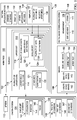
- workpiece 100 may be any object for which it is desirable to obtain any measurement using digital image correlation.
- Workpiece 100 may include any object made of any material.
- a dot pattern is applied on surface 102 of workpiece 100.
- Camera system 104 is used to obtain images 106 of the dot pattern on surface 102 of workpiece 100.
- Images 106 of workpiece 100 obtained by camera system 104 are provided to digital image correlation system 108 for processing.
- Digital image correlation system 108 may be configured to identify measurement 109 of workpiece 100 by digital image correlation of images 106 of workpiece 100.
- digital image correlation system 108 may be configured to use digital image correlation of images 106 of workpiece 100 taken at various points during a test to determine displacement 110 and strain 111 on workpiece 100 in response to stress 112 applied to workpiece 100.
- dot patterns over a range of multiple scales may be formed on surface 102 of workpiece 100.
- the multiple scale dot patterns may be applied over the same area on surface 102 of workpiece 100 in a manner so that dot patterns at smaller scales do not interfere with dot patterns at larger scales when images 106 of the dot patterns on surface 102 of workpiece 100 are used for digital image correlation.
- smaller scale dot patterns may be formed in a manner such that the smaller scale dot patterns form dots in the larger scale dot patterns of which they are a part.
- the dot pattern applied on surface 102 of workpiece 100 may include plurality of larger dots 113.
- Plurality of larger dots 113 may form larger scale dot pattern 114 on surface 102 of workpiece 100.
- larger scale dot pattern 114 may be applied over a relatively large portion of surface 102 of workpiece 100.
- Larger dot 116 may be one or more of plurality of larger dots 113 forming larger scale dot pattern 114.
- larger dot 116 may be formed of plurality of smaller dots 118.
- Plurality of smaller dots 118 may form smaller scale dot pattern 120 on surface 102 of workpiece 100. Smaller scale dot pattern 120 may thus be formed on a relatively small portion of surface 102 of workpiece 100 within the relatively larger portion of surface 102 that includes larger scale dot pattern 114.
- Plurality of larger dots 113 may include other dots 121 along with larger dot 116 to form larger scale dot pattern 114.
- Other dots 121 may or may not comprise plurality of smaller dots 118.
- other dots 121 may be substantially solid 122. In this application, including in the claims, a dot is considered substantially solid 122 if individual smaller dots cannot be distinguished within the dot for use in digital image correlation.
- Smaller dot 123 may be one or more of plurality of smaller dots 118 forming smaller scale dot pattern 120.
- smaller dot 123 may be formed of plurality of dots 124 forming dot pattern 126.
- dot pattern 126 may form a dot pattern that has a scale that is smaller than smaller scale dot pattern 120.
- Plurality of larger dots 113, plurality of smaller dots 118, and plurality of dots 124 are examples of dots forming various dot patterns of various different scales on surface 102 of workpiece 100.
- the dots forming the various dot patterns on surface 102 of workpiece 100 may be of any appropriate shape.
- the dots forming the various dot patterns on surface 102 of workpiece 100 may have any appropriate color or shading with respect to surface 102 of workpiece 100 on which they are applied, as long as such dots are distinguishable from surface 102 in images 106 of surface 102 obtained at the appropriate scale by camera system 104.
- the various dots forming the various dot patterns on surface 102 of workpiece 100 may be formed as darker dots on a lighter background or as lighter dots on a darker background.
- the dots forming the various dot patterns on surface 102 of workpiece 100 may be formed of any appropriate material. This material may be applied onto surface 102 of workpiece 100 to form the various dot patterns using any appropriate pattern application method 128.
- pattern application method 128 may include airbrush spraying 130 , printing 132, other application methods 134 , or any combination of application methods for applying an appropriate material onto surface 102 of workpiece 100 to form the various dot patterns.
- Pattern application method 128 may be controlled in any appropriate manner to form dot patterns of various different scales on surface 102 of workpiece 100.
- pattern application method 128 may include the use of template 136 to form dot patterns of various scales at defined locations on surface 102 of workpiece 100.
- Template 136 may have plurality of apertures 137 formed therein. Plurality of apertures 137 in template 136 may define positions of plurality of larger dots 113 on surface 102 of workpiece 100 when template 136 is placed on surface 102.
- Plurality of smaller dots 118 may be formed in areas on surface 102 of workpiece 100 defined by a number of selected apertures 138 in plurality of apertures 137 to form smaller scale dot pattern 120 within larger scale dot pattern 114 on surface 102 of workpiece 100.
- Other dots 121 may be formed in areas defined by other ones of plurality of apertures 137 to form the rest of larger scale dot pattern 114 on surface 102.
- Camera system 104 is configured to obtain images 106 of the various dot patterns on surface 102 of workpiece 100 for use by digital image correlation system 108.
- camera system 104 may be configured to obtain images 106 using various different fields of view corresponding to the various different scales of the dot patterns on surface 102 of workpiece 100.
- Any appropriate types of cameras for obtaining images 106 of surface 102 of workpiece 100 that may be appropriate for use by digital image correlation system 108 may be used to implement camera system 104.
- Camera system 104 may include single set of cameras 139 or multiple sets of cameras 140.
- Single set of cameras 139 may include a number of cameras for obtaining images 106 of workpiece 100.
- single set of cameras 139 may include two cameras for obtaining images 106 of workpiece 100 in a manner so that three dimensional measurements of workpiece 100 may be made using images 106.
- configuration 141 of single set of cameras 139 may be changed to change the field of view of single set of cameras 139 to obtain images 106 of workpiece 100 at different scales corresponding to the various different scales of the dot patterns on surface 102 of workpiece 100.
- single set of cameras 139 first may be configured to obtain larger scale images 142 of larger scale dot pattern 114 on surface 102 of workpiece 100.
- Configuration 141 of single set of cameras 139 then may be changed to change the field of view of single set of cameras 139 to obtain smaller scale images 143 of smaller scale dot pattern 120 on surface 102 of workpiece 100.
- configuration 141 of single set of cameras 139 may include position 144 and focus 145 of single set of cameras 139. Position 144 , focus 145 , or both position 144 and focus 145 of single set of cameras 139 may be changed as appropriate to obtain images 106 of workpiece 100 at different scales corresponding to the various different scales of the dot patterns on surface 102 of workpiece 100.
- first set of cameras 146 may be used to obtain larger scale images 142 of larger scale dot pattern 114 on workpiece 100 while second set of cameras 147 simultaneously obtains smaller scale images 143 of smaller scale dot pattern 120 on workpiece 100.
- camera system 104 may obtain images 106 of the various dot patterns of surface 102 of workpiece 100 before stress 112 is applied to workpiece 100. These images obtained before stress 112 is applied to workpiece 100 may be referred to as baseline images 150. Camera system 104 also may be used to obtain images 106 during test 152, while stress 112 is applied to workpiece 100. Camera system 104 also may be used to obtain images 106 after test 154, after stress 112 is removed from workpiece 100.
- Digital image correlation system 108 may use any appropriate method for processing images 106 using digital image correlation to identify various characteristics of workpiece 100.
- digital image correlation system 108 may be implemented using commercially available digital image correlation software such as ARAMIS by TRILION Quality Systems/GOM or VIC-3D by Correlated Systems.
- FIG. 1 The illustration of Figure 1 is not meant to imply physical or architectural limitations to the manner in which an illustrative embodiment may be implemented. Other components in addition to, in place of, or both in addition to and in place of the ones illustrated may be used. Some components may be unnecessary in some illustrative embodiments. Also, the blocks are presented to illustrate some functional components. One or more of these blocks may be combined or divided into different blocks when implemented in different illustrative embodiments.
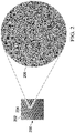
- workpiece 200 may be an example of one implementation of 100 in Figure 1 .
- Workpiece 200 may have larger scale dot pattern 202 formed thereon.
- Larger scale dot pattern 202 may include a plurality of larger dots formed on the surface of workpiece 200.
- dot 204 may be one of the larger dots forming larger scale dot pattern 202 .
- dot 204 An expanded view of dot 204 is shown on the right side of Figure 2 .
- larger dot 204 itself is formed of smaller scale dot pattern 206 .
- smaller scale dot pattern 206 When viewed by a camera system with a smaller scale field of view, smaller scale dot pattern 206 forming larger dot 204 is apparent.
- dot 204 that is larger appears to be one of the many dots forming larger scale dot pattern 202 .
- the presence of smaller scale dot pattern 206 does not affect the use of larger scale dot pattern 202 for digital image correlation.
- FIG. 3 an illustration of a flowchart of a process for multiple-scale digital image correlation is depicted in accordance with an illustrative embodiment.
- the process illustrated in Figure 3 may be used for digital image correlation measurements of workpiece 100 in
- operation 302 begins by applying multiple-scale dot patterns to a workpiece (operation 302 ).
- operation 302 may include applying a smaller scale dot pattern to a surface of the workpiece in which the smaller scale dot pattern forms a larger scale dot in a smaller scale dot pattern applied to the surface of the workpiece.
- a camera system then may be configured for viewing the larger scale dot pattern and the smaller scale dot pattern on the workpiece (operation 304 ) .
- the camera system then may be used to acquire baseline images of the larger scale dot pattern at a larger scale and baseline images of the smaller scale dot pattern at a smaller scale (operation 306 ).
- Stress then may be applied to the workpiece (operation 308 ).
- Images of the larger scale dot pattern may be obtained at a larger scale and images of the smaller scale dot pattern on the workpiece may be obtained at a smaller scale during the test at which stress is applied to the workpiece (operation 310 ) .
- the stress then may be removed from the workpiece (operation 312 ).
- Images of the larger scale dot pattern on the workpiece may be obtained and smaller scale images of the smaller scale dot pattern on the workpiece may be acquired after the stress is removed from the workpiece (operation 314 ).
- Digital image correlation of the baseline images and successive images then may be performed to determine a measurement of the workpiece (operation 316 ), with the process terminating thereafter.
- digital image correlation may be used to determine displacements and strains using the baseline images and the successive images of the larger scale dot pattern and of the smaller scale dot pattern on the workpiece
- FIG. 4 an illustration of a flowchart of a process for forming a multiple-scale dot pattern on a workpiece is depicted in accordance with an illustrative embodiment.
- the process illustrated in Figure 4 may be used to perform operation 302 in the process illustrated in Figure 3 .
- the process begins by applying smaller scale dot patterns at points of interest on a workpiece such that the smaller scale dot patterns form larger scale dots for a larger scale dot pattern (operation 402 ). Additional larger scale dots then may be applied to the surface of the workpiece to complete the larger scale dot pattern (operation 404 ), with the process terminating thereafter.
- each block in the flowcharts or block diagrams may represent a module, a segment, a function, and/or a portion of an operation or step.
- one or more of the blocks may be implemented as program code, in hardware, or a combination of the program code and hardware.
- the hardware may, for example, take the form of integrated circuits that are manufactured or configured to perform one or more operations in the flowcharts or block diagrams.
- the function or functions noted in the blocks may occur out of the order noted in the figures.
- two blocks shown in succession may be executed substantially concurrently, or the blocks may sometimes be performed in the reverse order, depending upon the functionality involved.
- other blocks may be added in addition to the illustrated blocks in a flowchart or block diagram.
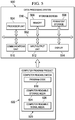
- data processing system 500 is an example of one implementation of a data processing system for implementing digital image correlation system 108 in Figure 1 .
- data processing system 500 includes communications fabric 502 .
- Communications fabric 502 provides communications between processor unit 504 , memory 506 , persistent storage 508 , communications unit 510 , input/output (I/O) unit 512 , and display 514 .
- Memory 506 , persistent storage 508 , communications unit 510 , input/output (I/O) unit 512 , and display 514 are examples of resources accessible by processor unit 504 via communications fabric 502 .
- Processor unit 504 serves to run instructions for software that may be loaded into memory 506 .
- Processor unit 504 may be a number of processors, a multi-processor core, or some other type of processor, depending on the particular implementation. Further, processor unit 504 may be implemented using a number of heterogeneous processor systems in which a main processor is present with secondary processors on a single chip. As another illustrative example, processor unit 504 may be a symmetric multi-processor system containing multiple processors of the same type.
- Memory 506 and persistent storage 508 are examples of storage devices 516.
- a storage device is any piece of hardware that is capable of storing information, such as, for example, without limitation, data, program code in functional form, and other suitable information either on a temporary basis or a permanent basis.
- Storage devices 516 also may be referred to as computer readable storage devices in these examples.
- Memory 506, in these examples, may be, for example, a random access memory or any other suitable volatile or non-volatile storage device.
- Persistent storage 508 may take various forms, depending on the particular implementation.
- persistent storage 508 may contain one or more components or devices.
- persistent storage 508 may be a hard drive, a flash memory, a rewritable optical disk, a rewritable magnetic tape, or some combination of the above.
- the media used by persistent storage 508 also may be removable.
- a removable hard drive may be used for persistent storage 508.
- Communications unit 510 in these examples, provides for communications with other data processing systems or devices.
- communications unit 510 is a network interface card.
- Communications unit 510 may provide communications through the use of either or both physical and wireless communications links.
- Input/output (I/O) unit 512 allows for input and output of data with other devices that may be connected to data processing system 500.
- input/output (I/O) unit 512 may provide a connection for user input through a keyboard, a mouse, and/or some other suitable input device. Further, input/output (I/O) unit 512 may send output to a printer.
- Display 514 provides a mechanism to display information to a user.
- Instructions for the operating system, applications, and/or programs may be located in storage devices 516 , which are in communication with processor unit 504 through communications fabric 502 .
- the instructions are in a functional form on persistent storage 508. These instructions may be loaded into memory 506 for execution by processor unit 504 .
- the processes of the different embodiments may be performed by processor unit 504 using computer-implemented instructions, which may be located in a memory, such as memory 506 .
- program instructions are referred to as program instructions, program code, computer usable program code, or computer readable program code that may be read and executed by a processor in processor unit 504 .
- the program code in the different embodiments may be embodied on different physical or computer readable storage media, such as memory 506 or persistent storage 508 .
- Program code 518 is located in a functional form on computer readable media 520 that is selectively removable and may be loaded onto or transferred to data processing system 500 for execution by processor unit 504 .
- Program code 518 and computer readable media 520 form computer program product 522 in these examples.
- computer readable media 520 may be computer readable storage media 524 or computer readable signal media 526.
- Computer readable storage media 524 may include, for example, an optical or magnetic disk that is inserted or placed into a drive or other device that is part of persistent storage 508 for transfer onto a storage device, such as a hard drive, that is part of persistent storage 508 .
- Computer readable storage media 524 also may take the form of a persistent storage, such as a hard drive, a thumb drive, or a flash memory, that is connected to data processing system 500. In some instances, computer readable storage media 524 may not be removable from data processing system 500 .
- computer readable storage media 524 is a physical or tangible storage device used to store program code 518 rather than a medium that propagates or transmits program code 518 .
- Computer readable storage media 524 is also referred to as a computer readable tangible storage device or a computer readable physical storage device. In other words, computer readable storage media 524 is a media that can be touched by a person.
- program code 518 may be transferred to data processing system 500 using computer readable signal media 526 .
- Computer readable signal media 526 may be, for example, a propagated data signal containing program code 518 .
- Computer readable signal media 526 may be an electromagnetic signal, an optical signal, and/or any other suitable type of signal. These signals may be transmitted over communications links, such as wireless communications links, optical fiber cable, coaxial cable, a wire, and/or any other suitable type of communications link.
- the communications link and/or the connection may be physical or wireless in the illustrative examples.
- program code 518 may be downloaded over a network to persistent storage 508 from another device or data processing system through computer readable signal media 526 for use within data processing system 500 .
- program code stored in a computer readable storage medium in a server data processing system may be downloaded over a network from the server to data processing system 500 .
- the data processing system providing program code 518 may be a server computer, a client computer, or some other device capable of storing and transmitting program code 518 .
- data processing system 500 may include organic components integrated with inorganic components and/or may be comprised entirely of organic components excluding a human being.
- a storage device may be comprised of an organic semiconductor.
- processor unit 504 may take the form of a hardware unit that has circuits that are manufactured or configured for a particular use. This type of hardware may perform operations without needing program code to be loaded into a memory from a storage device to be configured to perform the operations.
- processor unit 504 when processor unit 504 takes the form of a hardware unit, processor unit 504 may be a circuit system, an application specific integrated circuit (ASIC), a programmable logic device, or some other suitable type of hardware configured to perform a number of operations.
- ASIC application specific integrated circuit
- a programmable logic device the device is configured to perform the number of operations. The device may be reconfigured at a later time or may be permanently configured to perform the number of operations.
- Examples of programmable logic devices include, for example, a programmable logic array, a programmable array logic, a field programmable logic array, a field programmable gate array, and other suitable hardware devices.
- program code 518 may be omitted, because the processes for the different embodiments are implemented in a hardware unit.
- processor unit 504 may be implemented using a combination of processors found in computers and hardware units.
- Processor unit 504 may have a number of hardware units and a number of processors that are configured to run program code 518. With this depicted example, some of the processes may be implemented in the number of hardware units, while other processes may be implemented in the number of processors.
- a bus system may be used to implement communications fabric 502 and may be comprised of one or more buses, such as a system bus or an input/output bus.
- the bus system may be implemented using any suitable type of architecture that provides for a transfer of data between different components or devices attached to the bus system.
- communications unit 510 may include a number of devices that transmit data, receive data, or both transmit and receive data.
- Communications unit 510 may be, for example, a modem or a network adapter, two network adapters, or some combination thereof.
- a memory may be, for example, memory 506 , or a cache, such as that found in an interface and memory controller hub that may be present in communications fabric 502 .
- each block in the flowcharts or block diagrams may represent a module, segment, or portion of code, which comprises one or more executable instructions for implementing the specified logical function or functions.
- the functions noted in a block may occur out of the order noted in the figures. For example, the functions of two blocks shown in succession may be executed substantially concurrently, or the functions of the blocks may sometimes be executed in the reverse order, depending upon the functionality involved.
Landscapes
- Physics & Mathematics (AREA)
- General Physics & Mathematics (AREA)
- Engineering & Computer Science (AREA)
- Theoretical Computer Science (AREA)
- Computer Vision & Pattern Recognition (AREA)
- Immunology (AREA)
- Life Sciences & Earth Sciences (AREA)
- General Health & Medical Sciences (AREA)
- Analytical Chemistry (AREA)
- Pathology (AREA)
- Chemical & Material Sciences (AREA)
- Health & Medical Sciences (AREA)
- Biochemistry (AREA)
- Signal Processing (AREA)
- Multimedia (AREA)
- Length Measuring Devices By Optical Means (AREA)
- Image Analysis (AREA)
- Image Processing (AREA)
- Quality & Reliability (AREA)
Claims (14)
- System, das eine Kombination aus einem Werkstück (100), einem Kamerasystem (104) und einem digitalen Bildkorrelationssystem (108) aufweist, wobei das Werkstück aufweist:eine erste Vielzahl von Punkten auf einer Oberfläche (102) des Werkstücks (100), die ein erstes großflächiges Punktemuster bilden, wobei die erste Vielzahl von Punkten einen ersten Punkt aufweisen, wobei der erste Punkt eine zweite Vielzahl von Punkten aufweist, die ein zweites kleinflächiges Punktemuster bilden,wobei das Kamerasystem (104) dazu konfiguriert ist, großflächige Bilder des ersten großflächigen Punktemusters zu erhalten und das Kamerasystem dazu konfiguriert ist, kleinflächige Bilder des zweiten kleinflächigen Punktemusters (120) zu erhalten, undwobei das digitale Bildkorrelationssystem dazu konfiguriert ist, die großflächigen Bilder (142) und die kleinflächigen Bilder (143) zu verwenden, um eine Messung (109) des Werkstücks (100) zu bestimmen.
- System nach Anspruch 1, wobei die erste Vielzahl von Punkten eine Vielzahl von im Wesentlichen festen (122) Punkten aufweisen.
- System nach Anspruch 1, wobei:Positionen der ersten Vielzahl von Punkten auf der Oberfläche (102) durch eine Vorlage (136) definiert werden, die eine Vielzahl von Öffnungen (137) aufweist; unddie zweite Vielzahl von Punkten in Bereichen auf der Oberfläche (102) gebildet werden, die durch eine Anzahl ausgewählter Öffnungen (138) der Vielzahl von Öffnungen (137) definiert werden.
- System nach Anspruch 3, wobei die zweite Vielzahl von Punkten durch Airbrush- bzw. Spritzpistolen-Sprühen (130) in die Anzahl ausgewählter Öffnungen (138) auf der Oberfläche (102) aufgebracht werden.
- System nach Anspruch 1, wobei die zweite Vielzahl von Punkten durch Drucken (132) des zweiten Punktemusters auf die Oberfläche (102) auf der Oberfläche (102) aufgebracht werden.
- System nach Anspruch 1, wobei die zweite Vielzahl von Punkten einen zweiten Punkt aufweisen, und wobei der zweite Punkt eine dritte Vielzahl von Punkten aufweist, die ein drittes Punktemuster bilden.
- Verfahren zum Aufbringen eines mehrflächigen Punktemusters auf ein Werkstück (100), das aufweist:Aufbringen einer Vielzahl kleinerer Punkte (118) auf eine Oberfläche (102) des Werkstücks (100), um ein kleinflächiges Punktemuster (120) zu bilden, wobei die Vielzahl kleinerer Punkte (118) einen größeren Punkt (116) in einem großflächigen Muster (114) auf der Oberfläche (102) bilden;Aufbringen einer Vielzahl größerer Punkte (113) auf die Oberfläche (102), um das großflächige Punktemuster (114) zu bilden; undErhalten, durch ein Kamerasystem (104), großflächiger Bilder (142) des großflächigen Punktemusters (114),Erhalten, durch das Kamerasystem (104), kleinflächiger Bilder (143) des kleinflächigen Punktemusters (120); undVerwenden der großflächigen Bilder (142) und der kleinflächigen Bilder (143), um eine Messung (109) des Werkstücks (100) zu bestimmen.
- Verfahren nach Anspruch 7, wobei die Vielzahl größerer Punkte (113) eine Vielzahl i Wesentlichen fester (122) Punkte aufweisen.
- Verfahren nach Anspruch 7, das des Weiteren aufweist:Platzieren einer Vorlage (136), die eine Vielzahl von Öffnungen (137) aufweist, auf der Oberfläche (102);Aufbringen der Vielzahl kleinerer Punkte (118) in einem Bereich auf der Oberfläche (102), der durch eine Anzahl ausgewählter Öffnungen (138) der Vielzahl von Öffnungen (137) definiert wird; undAufbringen der Vielzahl größerer Punkte (113) auf der Oberfläche (102) in Bereichen, die durch die Vielzahl von Öffnungen (137) definiert werden.
- Verfahren nach Anspruch 9, wobei das Aufbringen der Vielzahl kleinerer Punkte (118) Airbrush- bzw. Spritzpistolen-Sprühen (130) in die Anzahl ausgewählter Öffnungen (138) aufweist.
- Verfahren nach Anspruch 7, wobei das Aufbringen der Vielzahl kleinerer Punkte (118) das Drucken (132) des kleinflächigen Punktemusters (120) auf die Oberfläche (102) aufweist.
- Verfahren nach Anspruch 7, wobei die großflächigen Bilder (142) und die kleinflächigen Bilder (143) gleichzeitig durch das Kamerasystem (104) erhalten werden.
- Verfahren nach Anspruch 7, wobei die Messung (109) ausgewählt wird aus einer Messung einer Verschiebung (110) des Werkstücks (110) und einer Messung einer Dehnung (111) auf dem Werkstück (100).
- Verfahren zur digitalen Bildkorrelation, das aufweist:Erhalten, durch ein Kamerasystem (104), großflächiger Bilder (142) eines großflächigen Punktemusters (114) auf einer Oberfläche (102) eines Werkstücks (100);Erhalten, durch das Kamerasystem (104), kleinflächiger Bilder (142) eines kleinflächigen Punktemusters (120) auf der Oberfläche (102) des Werkstücks (100), wobei das kleinflächige Punktemuster (120) einen größeren Punkt (116) in dem großflächigen Punktemuster (114) in den großflächigen Bildern (142) bildet; undVerwenden der großflächigen Bilder (142) und der kleinflächigen Bilder (142), um eine Messung (109) des Werkstücks (100) zu bestimmen.
Applications Claiming Priority (1)
| Application Number | Priority Date | Filing Date | Title |
|---|---|---|---|
| US13/706,838 US11455737B2 (en) | 2012-12-06 | 2012-12-06 | Multiple-scale digital image correlation pattern and measurement |
Publications (2)
| Publication Number | Publication Date |
|---|---|
| EP2741071A1 EP2741071A1 (de) | 2014-06-11 |
| EP2741071B1 true EP2741071B1 (de) | 2019-08-21 |
Family
ID=49882778
Family Applications (1)
| Application Number | Title | Priority Date | Filing Date |
|---|---|---|---|
| EP13195867.0A Active EP2741071B1 (de) | 2012-12-06 | 2013-12-05 | Mehrskaliges Digitalbildkorrelationsmuster und Messung |
Country Status (4)
| Country | Link |
|---|---|
| US (2) | US11455737B2 (de) |
| EP (1) | EP2741071B1 (de) |
| JP (1) | JP2014115281A (de) |
| CN (1) | CN103854280A (de) |
Families Citing this family (18)
| Publication number | Priority date | Publication date | Assignee | Title |
|---|---|---|---|---|
| US11455737B2 (en) | 2012-12-06 | 2022-09-27 | The Boeing Company | Multiple-scale digital image correlation pattern and measurement |
| US9443300B2 (en) | 2014-09-15 | 2016-09-13 | The Boeing Company | Systems and methods for analyzing a bondline |
| JP6404070B2 (ja) * | 2014-10-01 | 2018-10-10 | 国立研究開発法人産業技術総合研究所 | マルチスケール変形計測用格子パターンとその製作方法 |
| US9852330B1 (en) | 2015-07-27 | 2017-12-26 | United Launch Alliance, L.L.C. | System and method to enable the application of optical tracking techniques for generating dynamic quantities of interest with alias protection |
| US11354881B2 (en) | 2015-07-27 | 2022-06-07 | United Launch Alliance, L.L.C. | System and method to enable the application of optical tracking techniques for generating dynamic quantities of interest with alias protection |
| US20180120096A1 (en) * | 2015-08-24 | 2018-05-03 | Aerojet Rocketdyne, Inc. | Process for non-destructive testing using direct strain imaging |
| WO2017195154A2 (en) | 2016-05-13 | 2017-11-16 | Sabic Global Technologies B.V. | Evaluation of applications using digital image correlation techniques |
| US10481255B2 (en) | 2016-08-09 | 2019-11-19 | Aptiv Technologies Limited | Trailer dimension estimation with two dimensional radar and camera |
| RU2665323C1 (ru) * | 2017-06-07 | 2018-08-29 | Валентин Викторович Терауд | Способ измерения геометрических параметров и/или деформаций образца при высокотемпературном воздействии на него и система для его осуществления |
| US10228237B2 (en) * | 2017-07-12 | 2019-03-12 | The Boeing Company | Non-destructive optical method for determining minimum bond strength and proving bond efficacy |
| US10955540B2 (en) | 2017-12-01 | 2021-03-23 | Aptiv Technologies Limited | Detection system |
| US11276159B1 (en) | 2018-05-15 | 2022-03-15 | United Launch Alliance, L.L.C. | System and method for rocket engine health monitoring using digital image correlation (DIC) |
| US10838054B2 (en) | 2018-10-08 | 2020-11-17 | Aptiv Technologies Limited | Detection system and method |
| US11092668B2 (en) | 2019-02-07 | 2021-08-17 | Aptiv Technologies Limited | Trailer detection system and method |
| WO2020262087A1 (ja) * | 2019-06-26 | 2020-12-30 | 国立研究開発法人科学技術振興機構 | 応力およびひずみ量分布表示方法、装置およびプログラム |
| CN110779454B (zh) * | 2019-10-10 | 2020-08-11 | 北京科技大学 | 基于双通道结构散斑互相关算法的改进数字图像相关方法 |
| US11408995B2 (en) | 2020-02-24 | 2022-08-09 | Aptiv Technologies Limited | Lateral-bin monitoring for radar target detection |
| CN113536570B (zh) * | 2021-07-16 | 2022-09-27 | 中国石油大学(北京) | 一种应力参数计算方法、装置、系统及计算机设备 |
Citations (1)
| Publication number | Priority date | Publication date | Assignee | Title |
|---|---|---|---|---|
| WO2002019415A1 (en) * | 2000-08-30 | 2002-03-07 | Kla-Tencor Corporation | Overlay marks, methods of overlay mark design and methods of overlay measurements |
Family Cites Families (32)
| Publication number | Priority date | Publication date | Assignee | Title |
|---|---|---|---|---|
| US4600666A (en) | 1983-01-12 | 1986-07-15 | Zink Edmund S | Integrated photoscreen for making a halftone reproduction printing plate from a photograph |
| JPH08510851A (ja) * | 1993-03-25 | 1996-11-12 | ライブ ピクチャー,インコーポレイテッド | 画像処理方法及び装置 |
| US5608529A (en) * | 1994-01-31 | 1997-03-04 | Nikon Corporation | Optical three-dimensional shape measuring apparatus |
| US6567570B1 (en) * | 1998-10-30 | 2003-05-20 | Hewlett-Packard Development Company, L.P. | Optical image scanner with internal measurement of point-spread function and compensation for optical aberrations |
| JP3373831B2 (ja) * | 2000-01-19 | 2003-02-04 | 岸本産業株式会社 | 試験片の伸び測定方法及び装置 |
| US6480655B1 (en) | 2000-04-03 | 2002-11-12 | Meadewestvaco Corporation | Apparatus for the measurement of paperboard strain in a confined area |
| TW527518B (en) | 2000-07-14 | 2003-04-11 | Massachusetts Inst Technology | Method and system for high resolution, ultra fast, 3-D imaging |
| JP4616509B2 (ja) | 2001-05-11 | 2011-01-19 | 公三 藤本 | 位置決めマーカおよび位置決め装置 |
| JP3921968B2 (ja) | 2001-07-12 | 2007-05-30 | 株式会社豊田自動織機 | 位置検出方法及び位置検出装置 |
| FR2835603B1 (fr) | 2002-02-01 | 2004-11-12 | Holo 3 | Procede et dispositif de mesure optique du deplacement et/ou de la deformation d'un objet dans au moins une direction |
| US6774459B2 (en) | 2002-08-13 | 2004-08-10 | Micron Technology, Inc. | Capacitor layout technique for reduction of fixed pattern noise in a CMOS sensor |
| TWI271583B (en) | 2004-03-09 | 2007-01-21 | Au Optronics Corp | Light guide of backlight unit |
| US7154613B2 (en) * | 2004-03-15 | 2006-12-26 | Northrop Grumman Corporation | Color coded light for automated shape measurement using photogrammetry |
| US7080561B2 (en) | 2004-09-27 | 2006-07-25 | The Boeing Company | Visual documentation of micro-cracks during tensile coupon testing |
| JP4730836B2 (ja) * | 2005-09-15 | 2011-07-20 | Jfeスチール株式会社 | 面歪の測定装置及び方法 |
| CN100458359C (zh) * | 2006-03-02 | 2009-02-04 | 浣石 | 远距离面内小位移测量系统 |
| US7377181B2 (en) | 2006-03-10 | 2008-05-27 | Northrop Grumman Corporation | In-situ large area optical strain measurement using an encoded dot pattern |
| JP2008031702A (ja) | 2006-07-27 | 2008-02-14 | Kubota Matsushitadenko Exterior Works Ltd | 建築板及びコーナー部材の製造方法 |
| US9957157B2 (en) | 2006-09-19 | 2018-05-01 | University of Houtson System | Fabrication of self assembling nano-structures |
| JP5029424B2 (ja) | 2008-02-28 | 2012-09-19 | Jfeスチール株式会社 | 張り剛性測定方法および装置 |
| JP5322206B2 (ja) * | 2008-05-07 | 2013-10-23 | 国立大学法人 香川大学 | 3次元形状の計測方法および装置 |
| JP5152058B2 (ja) * | 2009-03-19 | 2013-02-27 | セイコーエプソン株式会社 | 液滴吐出ヘッドの検査方法、液滴吐出ヘッドの検査装置及び液滴吐出装置 |
| US8600147B2 (en) * | 2009-06-03 | 2013-12-03 | The United States of America as represented by the Secreatary of the Navy | System and method for remote measurement of displacement and strain fields |
| JP5429864B2 (ja) | 2009-07-24 | 2014-02-26 | 独立行政法人物質・材料研究機構 | 歪み計測用パターン |
| US20120133920A1 (en) | 2009-09-22 | 2012-05-31 | Skunes Timothy A | High speed, high resolution, three dimensional printed circuit board inspection system |
| US8309278B2 (en) | 2010-07-07 | 2012-11-13 | Massachusetts Institute Of Technology | Guided self-assembly of block copolymer line structures for integrated circuit interconnects |
| WO2012006431A2 (en) | 2010-07-09 | 2012-01-12 | Temple University - Of The Commonwealth System Of Higher Education | Apparatus and method for surface and subsurface tactile sensation imaging |
| WO2013019992A1 (en) * | 2011-08-02 | 2013-02-07 | The Government Of The United States Of America, As Represented By The Secretary Of The Navy | System and method for remote full field three-dimensional displacement and strain measurements |
| US8818078B2 (en) | 2012-02-03 | 2014-08-26 | Solar Turbines Inc. | Apparatus and method for optically measuring creep |
| US9311566B2 (en) * | 2012-08-03 | 2016-04-12 | George Mason Research Foundation, Inc. | Method and system for direct strain imaging |
| US11455737B2 (en) | 2012-12-06 | 2022-09-27 | The Boeing Company | Multiple-scale digital image correlation pattern and measurement |
| US9645012B2 (en) * | 2015-08-17 | 2017-05-09 | The Boeing Company | Rapid automated infrared thermography for inspecting large composite structures |
-
2012
- 2012-12-06 US US13/706,838 patent/US11455737B2/en active Active
-
2013
- 2013-11-27 JP JP2013244591A patent/JP2014115281A/ja active Pending
- 2013-12-05 EP EP13195867.0A patent/EP2741071B1/de active Active
- 2013-12-05 CN CN201310652953.1A patent/CN103854280A/zh active Pending
-
2016
- 2016-05-11 US US15/152,151 patent/US11100657B2/en active Active
Patent Citations (1)
| Publication number | Priority date | Publication date | Assignee | Title |
|---|---|---|---|---|
| WO2002019415A1 (en) * | 2000-08-30 | 2002-03-07 | Kla-Tencor Corporation | Overlay marks, methods of overlay mark design and methods of overlay measurements |
Also Published As
| Publication number | Publication date |
|---|---|
| US20160253796A1 (en) | 2016-09-01 |
| US20140160279A1 (en) | 2014-06-12 |
| CN103854280A (zh) | 2014-06-11 |
| EP2741071A1 (de) | 2014-06-11 |
| US11455737B2 (en) | 2022-09-27 |
| US11100657B2 (en) | 2021-08-24 |
| JP2014115281A (ja) | 2014-06-26 |
Similar Documents
| Publication | Publication Date | Title |
|---|---|---|
| US11100657B2 (en) | Multiple-scale digital image correlation pattern and measurement | |
| CN110555889B (zh) | 一种基于CALTag和点云信息的深度相机手眼标定方法 | |
| JP4206057B2 (ja) | 光学式触覚センサを用いた力ベクトル再構成法 | |
| CN104713885B (zh) | 一种用于pcb板在线检测的结构光辅助双目测量方法 | |
| US8600147B2 (en) | System and method for remote measurement of displacement and strain fields | |
| KR101690965B1 (ko) | 부정확한 캘리브레이션 타겟을 사용하는 머신 비전 시스템 캘리브레이션 | |
| US10771776B2 (en) | Apparatus and method for generating a camera model for an imaging system | |
| JP6072897B2 (ja) | スクリーンプリンタ装備の補正方法及びそれを用いた基板検査システム | |
| CN102183214B (zh) | 一种大口径非球面镜结构光检测方法 | |
| US8037744B2 (en) | Method for measuring deformation of tire tread | |
| CN105763870B (zh) | 一种十字线立体测试标版及其形成方法 | |
| JP2012058076A (ja) | 3次元計測装置及び3次元計測方法 | |
| CN109690622A (zh) | 多相机系统中的相机登记 | |
| TW201104508A (en) | Stereoscopic form reader | |
| CN113281723B (zh) | 一种基于AR tag的3D激光雷达与相机间结构参数的标定方法 | |
| CN109544643A (zh) | 一种摄像机图像校正方法及装置 | |
| JP2015049200A (ja) | 計測装置、方法及びプログラム | |
| RS62264B1 (sr) | Sistem mašinskog vida | |
| CN103148806A (zh) | 基于投影与多目视觉的船舶钢板动态三维测量系统 | |
| US11120576B1 (en) | Coarse to fine calibration parameter validation and temperature mitigation | |
| Cao et al. | Full‐field out‐of‐plane vibration displacement acquisition based on speckle‐projection digital image correlation and its application in damage localization | |
| JP5477658B2 (ja) | キャリブレーション用校正治具、校正治具を備えた3次元計測システム | |
| CN102313515B (zh) | 三维数字影像相关法的校正方法 | |
| CN106969719A (zh) | 一种光纤阵列纤芯间距的检测方法及装置 | |
| CN118347423B (zh) | 一种构件三维变形场信息的获取方法和装置 |
Legal Events
| Date | Code | Title | Description |
|---|---|---|---|
| PUAI | Public reference made under article 153(3) epc to a published international application that has entered the european phase |
Free format text: ORIGINAL CODE: 0009012 |
|
| 17P | Request for examination filed |
Effective date: 20131205 |
|
| AK | Designated contracting states |
Kind code of ref document: A1 Designated state(s): AL AT BE BG CH CY CZ DE DK EE ES FI FR GB GR HR HU IE IS IT LI LT LU LV MC MK MT NL NO PL PT RO RS SE SI SK SM TR |
|
| AX | Request for extension of the european patent |
Extension state: BA ME |
|
| RIN1 | Information on inventor provided before grant (corrected) |
Inventor name: PILLERS, JAMES E Inventor name: MCCRARY, KEVIN EARL Inventor name: GROSSNICKLE, JAMES A |
|
| GRAP | Despatch of communication of intention to grant a patent |
Free format text: ORIGINAL CODE: EPIDOSNIGR1 |
|
| STAA | Information on the status of an ep patent application or granted ep patent |
Free format text: STATUS: GRANT OF PATENT IS INTENDED |
|
| INTG | Intention to grant announced |
Effective date: 20190318 |
|
| GRAS | Grant fee paid |
Free format text: ORIGINAL CODE: EPIDOSNIGR3 |
|
| GRAA | (expected) grant |
Free format text: ORIGINAL CODE: 0009210 |
|
| STAA | Information on the status of an ep patent application or granted ep patent |
Free format text: STATUS: THE PATENT HAS BEEN GRANTED |
|
| AK | Designated contracting states |
Kind code of ref document: B1 Designated state(s): AL AT BE BG CH CY CZ DE DK EE ES FI FR GB GR HR HU IE IS IT LI LT LU LV MC MK MT NL NO PL PT RO RS SE SI SK SM TR |
|
| REG | Reference to a national code |
Ref country code: GB Ref legal event code: FG4D |
|
| REG | Reference to a national code |
Ref country code: CH Ref legal event code: EP |
|
| REG | Reference to a national code |
Ref country code: DE Ref legal event code: R096 Ref document number: 602013059405 Country of ref document: DE |
|
| REG | Reference to a national code |
Ref country code: AT Ref legal event code: REF Ref document number: 1170292 Country of ref document: AT Kind code of ref document: T Effective date: 20190915 |
|
| REG | Reference to a national code |
Ref country code: IE Ref legal event code: FG4D |
|
| REG | Reference to a national code |
Ref country code: LT Ref legal event code: MG4D |
|
| REG | Reference to a national code |
Ref country code: NL Ref legal event code: MP Effective date: 20190821 |
|
| PG25 | Lapsed in a contracting state [announced via postgrant information from national office to epo] |
Ref country code: PT Free format text: LAPSE BECAUSE OF FAILURE TO SUBMIT A TRANSLATION OF THE DESCRIPTION OR TO PAY THE FEE WITHIN THE PRESCRIBED TIME-LIMIT Effective date: 20191223 Ref country code: HR Free format text: LAPSE BECAUSE OF FAILURE TO SUBMIT A TRANSLATION OF THE DESCRIPTION OR TO PAY THE FEE WITHIN THE PRESCRIBED TIME-LIMIT Effective date: 20190821 Ref country code: LT Free format text: LAPSE BECAUSE OF FAILURE TO SUBMIT A TRANSLATION OF THE DESCRIPTION OR TO PAY THE FEE WITHIN THE PRESCRIBED TIME-LIMIT Effective date: 20190821 Ref country code: BG Free format text: LAPSE BECAUSE OF FAILURE TO SUBMIT A TRANSLATION OF THE DESCRIPTION OR TO PAY THE FEE WITHIN THE PRESCRIBED TIME-LIMIT Effective date: 20191121 Ref country code: SE Free format text: LAPSE BECAUSE OF FAILURE TO SUBMIT A TRANSLATION OF THE DESCRIPTION OR TO PAY THE FEE WITHIN THE PRESCRIBED TIME-LIMIT Effective date: 20190821 Ref country code: NL Free format text: LAPSE BECAUSE OF FAILURE TO SUBMIT A TRANSLATION OF THE DESCRIPTION OR TO PAY THE FEE WITHIN THE PRESCRIBED TIME-LIMIT Effective date: 20190821 Ref country code: FI Free format text: LAPSE BECAUSE OF FAILURE TO SUBMIT A TRANSLATION OF THE DESCRIPTION OR TO PAY THE FEE WITHIN THE PRESCRIBED TIME-LIMIT Effective date: 20190821 Ref country code: NO Free format text: LAPSE BECAUSE OF FAILURE TO SUBMIT A TRANSLATION OF THE DESCRIPTION OR TO PAY THE FEE WITHIN THE PRESCRIBED TIME-LIMIT Effective date: 20191121 |
|
| PG25 | Lapsed in a contracting state [announced via postgrant information from national office to epo] |
Ref country code: ES Free format text: LAPSE BECAUSE OF FAILURE TO SUBMIT A TRANSLATION OF THE DESCRIPTION OR TO PAY THE FEE WITHIN THE PRESCRIBED TIME-LIMIT Effective date: 20190821 Ref country code: RS Free format text: LAPSE BECAUSE OF FAILURE TO SUBMIT A TRANSLATION OF THE DESCRIPTION OR TO PAY THE FEE WITHIN THE PRESCRIBED TIME-LIMIT Effective date: 20190821 Ref country code: LV Free format text: LAPSE BECAUSE OF FAILURE TO SUBMIT A TRANSLATION OF THE DESCRIPTION OR TO PAY THE FEE WITHIN THE PRESCRIBED TIME-LIMIT Effective date: 20190821 Ref country code: IS Free format text: LAPSE BECAUSE OF FAILURE TO SUBMIT A TRANSLATION OF THE DESCRIPTION OR TO PAY THE FEE WITHIN THE PRESCRIBED TIME-LIMIT Effective date: 20191221 Ref country code: AL Free format text: LAPSE BECAUSE OF FAILURE TO SUBMIT A TRANSLATION OF THE DESCRIPTION OR TO PAY THE FEE WITHIN THE PRESCRIBED TIME-LIMIT Effective date: 20190821 Ref country code: GR Free format text: LAPSE BECAUSE OF FAILURE TO SUBMIT A TRANSLATION OF THE DESCRIPTION OR TO PAY THE FEE WITHIN THE PRESCRIBED TIME-LIMIT Effective date: 20191122 |
|
| REG | Reference to a national code |
Ref country code: AT Ref legal event code: MK05 Ref document number: 1170292 Country of ref document: AT Kind code of ref document: T Effective date: 20190821 |
|
| PG25 | Lapsed in a contracting state [announced via postgrant information from national office to epo] |
Ref country code: TR Free format text: LAPSE BECAUSE OF FAILURE TO SUBMIT A TRANSLATION OF THE DESCRIPTION OR TO PAY THE FEE WITHIN THE PRESCRIBED TIME-LIMIT Effective date: 20190821 |
|
| PG25 | Lapsed in a contracting state [announced via postgrant information from national office to epo] |
Ref country code: IT Free format text: LAPSE BECAUSE OF FAILURE TO SUBMIT A TRANSLATION OF THE DESCRIPTION OR TO PAY THE FEE WITHIN THE PRESCRIBED TIME-LIMIT Effective date: 20190821 Ref country code: RO Free format text: LAPSE BECAUSE OF FAILURE TO SUBMIT A TRANSLATION OF THE DESCRIPTION OR TO PAY THE FEE WITHIN THE PRESCRIBED TIME-LIMIT Effective date: 20190821 Ref country code: EE Free format text: LAPSE BECAUSE OF FAILURE TO SUBMIT A TRANSLATION OF THE DESCRIPTION OR TO PAY THE FEE WITHIN THE PRESCRIBED TIME-LIMIT Effective date: 20190821 Ref country code: AT Free format text: LAPSE BECAUSE OF FAILURE TO SUBMIT A TRANSLATION OF THE DESCRIPTION OR TO PAY THE FEE WITHIN THE PRESCRIBED TIME-LIMIT Effective date: 20190821 Ref country code: DK Free format text: LAPSE BECAUSE OF FAILURE TO SUBMIT A TRANSLATION OF THE DESCRIPTION OR TO PAY THE FEE WITHIN THE PRESCRIBED TIME-LIMIT Effective date: 20190821 Ref country code: PL Free format text: LAPSE BECAUSE OF FAILURE TO SUBMIT A TRANSLATION OF THE DESCRIPTION OR TO PAY THE FEE WITHIN THE PRESCRIBED TIME-LIMIT Effective date: 20190821 |
|
| PG25 | Lapsed in a contracting state [announced via postgrant information from national office to epo] |
Ref country code: IS Free format text: LAPSE BECAUSE OF FAILURE TO SUBMIT A TRANSLATION OF THE DESCRIPTION OR TO PAY THE FEE WITHIN THE PRESCRIBED TIME-LIMIT Effective date: 20200224 Ref country code: SK Free format text: LAPSE BECAUSE OF FAILURE TO SUBMIT A TRANSLATION OF THE DESCRIPTION OR TO PAY THE FEE WITHIN THE PRESCRIBED TIME-LIMIT Effective date: 20190821 Ref country code: SM Free format text: LAPSE BECAUSE OF FAILURE TO SUBMIT A TRANSLATION OF THE DESCRIPTION OR TO PAY THE FEE WITHIN THE PRESCRIBED TIME-LIMIT Effective date: 20190821 Ref country code: CZ Free format text: LAPSE BECAUSE OF FAILURE TO SUBMIT A TRANSLATION OF THE DESCRIPTION OR TO PAY THE FEE WITHIN THE PRESCRIBED TIME-LIMIT Effective date: 20190821 |
|
| REG | Reference to a national code |
Ref country code: DE Ref legal event code: R097 Ref document number: 602013059405 Country of ref document: DE |
|
| PLBE | No opposition filed within time limit |
Free format text: ORIGINAL CODE: 0009261 |
|
| STAA | Information on the status of an ep patent application or granted ep patent |
Free format text: STATUS: NO OPPOSITION FILED WITHIN TIME LIMIT |
|
| PG2D | Information on lapse in contracting state deleted |
Ref country code: IS |
|
| REG | Reference to a national code |
Ref country code: CH Ref legal event code: PL |
|
| 26N | No opposition filed |
Effective date: 20200603 |
|
| REG | Reference to a national code |
Ref country code: BE Ref legal event code: MM Effective date: 20191231 |
|
| PG25 | Lapsed in a contracting state [announced via postgrant information from national office to epo] |
Ref country code: MC Free format text: LAPSE BECAUSE OF FAILURE TO SUBMIT A TRANSLATION OF THE DESCRIPTION OR TO PAY THE FEE WITHIN THE PRESCRIBED TIME-LIMIT Effective date: 20190821 Ref country code: SI Free format text: LAPSE BECAUSE OF FAILURE TO SUBMIT A TRANSLATION OF THE DESCRIPTION OR TO PAY THE FEE WITHIN THE PRESCRIBED TIME-LIMIT Effective date: 20190821 |
|
| PG25 | Lapsed in a contracting state [announced via postgrant information from national office to epo] |
Ref country code: IE Free format text: LAPSE BECAUSE OF NON-PAYMENT OF DUE FEES Effective date: 20191205 Ref country code: LU Free format text: LAPSE BECAUSE OF NON-PAYMENT OF DUE FEES Effective date: 20191205 |
|
| PG25 | Lapsed in a contracting state [announced via postgrant information from national office to epo] |
Ref country code: BE Free format text: LAPSE BECAUSE OF NON-PAYMENT OF DUE FEES Effective date: 20191231 Ref country code: LI Free format text: LAPSE BECAUSE OF NON-PAYMENT OF DUE FEES Effective date: 20191231 Ref country code: CH Free format text: LAPSE BECAUSE OF NON-PAYMENT OF DUE FEES Effective date: 20191231 |
|
| PG25 | Lapsed in a contracting state [announced via postgrant information from national office to epo] |
Ref country code: CY Free format text: LAPSE BECAUSE OF FAILURE TO SUBMIT A TRANSLATION OF THE DESCRIPTION OR TO PAY THE FEE WITHIN THE PRESCRIBED TIME-LIMIT Effective date: 20190821 |
|
| PG25 | Lapsed in a contracting state [announced via postgrant information from national office to epo] |
Ref country code: MT Free format text: LAPSE BECAUSE OF FAILURE TO SUBMIT A TRANSLATION OF THE DESCRIPTION OR TO PAY THE FEE WITHIN THE PRESCRIBED TIME-LIMIT Effective date: 20190821 Ref country code: HU Free format text: LAPSE BECAUSE OF FAILURE TO SUBMIT A TRANSLATION OF THE DESCRIPTION OR TO PAY THE FEE WITHIN THE PRESCRIBED TIME-LIMIT; INVALID AB INITIO Effective date: 20131205 |
|
| PG25 | Lapsed in a contracting state [announced via postgrant information from national office to epo] |
Ref country code: MK Free format text: LAPSE BECAUSE OF FAILURE TO SUBMIT A TRANSLATION OF THE DESCRIPTION OR TO PAY THE FEE WITHIN THE PRESCRIBED TIME-LIMIT Effective date: 20190821 |
|
| P01 | Opt-out of the competence of the unified patent court (upc) registered |
Effective date: 20230516 |
|
| PGFP | Annual fee paid to national office [announced via postgrant information from national office to epo] |
Ref country code: GB Payment date: 20251229 Year of fee payment: 13 |
|
| PGFP | Annual fee paid to national office [announced via postgrant information from national office to epo] |
Ref country code: FR Payment date: 20251226 Year of fee payment: 13 |
|
| PGFP | Annual fee paid to national office [announced via postgrant information from national office to epo] |
Ref country code: DE Payment date: 20251229 Year of fee payment: 13 |