EP2740262B1 - Modes de lecture sensibles à la position pour des réseaux de photomultiplicateurs numériques en silicium - Google Patents
Modes de lecture sensibles à la position pour des réseaux de photomultiplicateurs numériques en silicium Download PDFInfo
- Publication number
- EP2740262B1 EP2740262B1 EP12772430.0A EP12772430A EP2740262B1 EP 2740262 B1 EP2740262 B1 EP 2740262B1 EP 12772430 A EP12772430 A EP 12772430A EP 2740262 B1 EP2740262 B1 EP 2740262B1
- Authority
- EP
- European Patent Office
- Prior art keywords
- latches
- detector
- photon
- spad
- circuitry
- Prior art date
- Legal status (The legal status is an assumption and is not a legal conclusion. Google has not performed a legal analysis and makes no representation as to the accuracy of the status listed.)
- Active
Links
- XUIMIQQOPSSXEZ-UHFFFAOYSA-N Silicon Chemical compound [Si] XUIMIQQOPSSXEZ-UHFFFAOYSA-N 0.000 title claims description 21
- 229910052710 silicon Inorganic materials 0.000 title claims description 21
- 239000010703 silicon Substances 0.000 title claims description 21
- 238000003491 array Methods 0.000 title description 2
- 238000001514 detection method Methods 0.000 claims description 38
- 230000010354 integration Effects 0.000 claims description 23
- 238000012545 processing Methods 0.000 claims description 17
- 230000015556 catabolic process Effects 0.000 claims description 12
- 238000002600 positron emission tomography Methods 0.000 claims description 12
- 230000005855 radiation Effects 0.000 claims description 11
- 238000003384 imaging method Methods 0.000 claims description 9
- 239000002245 particle Substances 0.000 claims description 9
- 238000000034 method Methods 0.000 claims description 7
- 230000001934 delay Effects 0.000 claims description 5
- 239000000758 substrate Substances 0.000 claims description 4
- 238000006243 chemical reaction Methods 0.000 claims description 3
- 230000001960 triggered effect Effects 0.000 claims description 2
- 230000003111 delayed effect Effects 0.000 claims 1
- 238000010791 quenching Methods 0.000 description 24
- 238000005259 measurement Methods 0.000 description 13
- 230000000171 quenching effect Effects 0.000 description 12
- 230000002123 temporal effect Effects 0.000 description 11
- 230000001364 causal effect Effects 0.000 description 10
- 238000013461 design Methods 0.000 description 7
- 230000004907 flux Effects 0.000 description 6
- 238000013459 approach Methods 0.000 description 4
- 230000008901 benefit Effects 0.000 description 4
- 230000005540 biological transmission Effects 0.000 description 4
- 230000008569 process Effects 0.000 description 3
- 230000004044 response Effects 0.000 description 3
- 230000002441 reversible effect Effects 0.000 description 3
- 230000007704 transition Effects 0.000 description 3
- 238000012879 PET imaging Methods 0.000 description 2
- 229910000676 Si alloy Inorganic materials 0.000 description 2
- 230000004075 alteration Effects 0.000 description 2
- 239000003989 dielectric material Substances 0.000 description 2
- 238000012986 modification Methods 0.000 description 2
- 230000004048 modification Effects 0.000 description 2
- 238000011112 process operation Methods 0.000 description 2
- 238000002603 single-photon emission computed tomography Methods 0.000 description 2
- 238000003325 tomography Methods 0.000 description 2
- 229910001339 C alloy Inorganic materials 0.000 description 1
- 229910000577 Silicon-germanium Inorganic materials 0.000 description 1
- AXQKVSDUCKWEKE-UHFFFAOYSA-N [C].[Ge].[Si] Chemical compound [C].[Ge].[Si] AXQKVSDUCKWEKE-UHFFFAOYSA-N 0.000 description 1
- LEVVHYCKPQWKOP-UHFFFAOYSA-N [Si].[Ge] Chemical compound [Si].[Ge] LEVVHYCKPQWKOP-UHFFFAOYSA-N 0.000 description 1
- 230000002776 aggregation Effects 0.000 description 1
- 238000004220 aggregation Methods 0.000 description 1
- 239000000956 alloy Substances 0.000 description 1
- 230000003139 buffering effect Effects 0.000 description 1
- 239000003990 capacitor Substances 0.000 description 1
- 230000001419 dependent effect Effects 0.000 description 1
- 238000002059 diagnostic imaging Methods 0.000 description 1
- 238000009826 distribution Methods 0.000 description 1
- 230000000694 effects Effects 0.000 description 1
- 230000005670 electromagnetic radiation Effects 0.000 description 1
- 239000012212 insulator Substances 0.000 description 1
- 238000000691 measurement method Methods 0.000 description 1
- 229910052751 metal Inorganic materials 0.000 description 1
- 239000002184 metal Substances 0.000 description 1
- 229910001092 metal group alloy Inorganic materials 0.000 description 1
- 150000002739 metals Chemical class 0.000 description 1
- 150000004767 nitrides Chemical class 0.000 description 1
- 230000003287 optical effect Effects 0.000 description 1
- 238000012636 positron electron tomography Methods 0.000 description 1
- 230000000717 retained effect Effects 0.000 description 1
- 238000005070 sampling Methods 0.000 description 1
- LIVNPJMFVYWSIS-UHFFFAOYSA-N silicon monoxide Chemical class [Si-]#[O+] LIVNPJMFVYWSIS-UHFFFAOYSA-N 0.000 description 1
- 229910052814 silicon oxide Inorganic materials 0.000 description 1
- 238000012358 sourcing Methods 0.000 description 1
- 238000003860 storage Methods 0.000 description 1
- 238000001429 visible spectrum Methods 0.000 description 1
Images


Classifications
-
- G—PHYSICS
- G01—MEASURING; TESTING
- G01T—MEASUREMENT OF NUCLEAR OR X-RADIATION
- G01T1/00—Measuring X-radiation, gamma radiation, corpuscular radiation, or cosmic radiation
- G01T1/16—Measuring radiation intensity
- G01T1/20—Measuring radiation intensity with scintillation detectors
- G01T1/2018—Scintillation-photodiode combinations
- G01T1/20184—Detector read-out circuitry, e.g. for clearing of traps, compensating for traps or compensating for direct hits
-
- G—PHYSICS
- G01—MEASURING; TESTING
- G01T—MEASUREMENT OF NUCLEAR OR X-RADIATION
- G01T1/00—Measuring X-radiation, gamma radiation, corpuscular radiation, or cosmic radiation
- G01T1/16—Measuring radiation intensity
- G01T1/24—Measuring radiation intensity with semiconductor detectors
- G01T1/248—Silicon photomultipliers [SiPM], e.g. an avalanche photodiode [APD] array on a common Si substrate
-
- G—PHYSICS
- G01—MEASURING; TESTING
- G01T—MEASUREMENT OF NUCLEAR OR X-RADIATION
- G01T1/00—Measuring X-radiation, gamma radiation, corpuscular radiation, or cosmic radiation
- G01T1/16—Measuring radiation intensity
- G01T1/24—Measuring radiation intensity with semiconductor detectors
- G01T1/249—Measuring radiation intensity with semiconductor detectors specially adapted for use in SPECT or PET
-
- G—PHYSICS
- G01—MEASURING; TESTING
- G01T—MEASUREMENT OF NUCLEAR OR X-RADIATION
- G01T1/00—Measuring X-radiation, gamma radiation, corpuscular radiation, or cosmic radiation
- G01T1/29—Measurement performed on radiation beams, e.g. position or section of the beam; Measurement of spatial distribution of radiation
- G01T1/2914—Measurement of spatial distribution of radiation
- G01T1/2985—In depth localisation, e.g. using positron emitters; Tomographic imaging (longitudinal and transverse section imaging; apparatus for radiation diagnosis sequentially in different planes, steroscopic radiation diagnosis)
-
- H—ELECTRICITY
- H04—ELECTRIC COMMUNICATION TECHNIQUE
- H04N—PICTORIAL COMMUNICATION, e.g. TELEVISION
- H04N25/00—Circuitry of solid-state image sensors [SSIS]; Control thereof
- H04N25/70—SSIS architectures; Circuits associated therewith
Definitions
- the following relates to the radiation detection arts. It particularly relates to high-speed and high spatial resolution radiation detectors for applications in physics, astronomy, radiological imaging such as positron emission tomography (PET) or single-photon emission tomography (SPECT), or so forth.
- PET positron emission tomography
- SPECT single-photon emission tomography
- Photon counting light detection finds application in diverse fields such as physics, astronomy, and medical imaging.
- photon counting light detection is useful in physics application such as Cherenkov detectors, engineering applications such as light detection and ranging (LIDAR) applications, biology applications such as low-light fluorescence measurements, low-light astronomical telescope facilities, and so forth.
- the term “photon” refers to a quantum particle of electromagnetic radiation.
- the term “photon” encompasses visible light photons, e.g. a 1.96 eV photon corresponding to one quantum particle of 632.8 nm HeNe laser light.
- the term “photon” also encompasses a quantum particle of "light” or electromagnetic energy lying outside of the visible spectrum.
- the term “photon” also encompasses a quantum particle of ultraviolet or infrared radiation).
- Photon counting has conventionally been implemented using photomultiplier tube (PMT) detectors, which comprise a light-sensitive photocathode and a set of "multiplier" anode terminals.
- the photocathode emits at least one electron responsive to impingement of a photon, and the electron(s) in turn strike successive anode terminals with each such event causing emission of a cascade of electrons, thus producing a multiplication effect that results in a measurable electrical pulse.
- a PMT is capable of high speed photon counting.
- PMT detectors have disadvantages including being relatively bulky discrete devices with large optical windows that operate at high voltage and are susceptible to failure due to the evacuated tube design and the high operational electrical voltage.
- SiPM devices have been developed to overcome some of these disadvantages, and to provide photon-counting detectors that are readily integrated with silicon-based signal/data processing circuitry.
- a SiPM device employs an avalanche photodiode as the light sensor. When biased above its breakdown voltage, the avalanche diode goes into break down responsive to impingement of a single photon. Such a device is sometimes called a single photon avalanche diode (SPAD) detector. In a typical SPAD detector, the avalanche photodiode is reverse biased above its break down voltage and is in series with a quenching resistor.
- SPAD single photon avalanche diode
- Impingement of a single photon causes the p-n junction to break down in a multiplicative (i.e., "avalanche") cascade of electrons that flow in the SPAD detector as a measurable electrical current.
- This current is quenched relatively quickly as voltage over the resistor due to the current flow lowers the reverse bias across the avalanche diode to a level below its break down voltage.
- an active quenching sub-circuit comprising (for example) one or more diodes, resistors, and/or transistors can provide more rapid quenching.
- a SPAD detector is relatively small, but larger area detection can be achieved by a two-dimensional array of SPAD detectors.
- the readout can be analog or digital.
- the SPAD detectors are interconnected in a logical "OR" circuit so that break down of any one SPAD detector activates the logical "OR" combination.
- the array operates a digital counter that is read out after an integration period. In either case, the readout circuitry has a single channel.
- time-of-flight positron emission tomography imaging
- the time of detection is important.
- silicon-based time stamping including time-to-digital conversion (TDC) circuitry can be monolithically integrated with a SPAD array on a silicon platform this purpose.
- US 2006/0202129 A1 discloses an integrated circuit that has an array of SPADs and trigger circuitry configured to generate a trigger signal responsive to break down of a SPAD of the array. Latches are provided that are configured to latch responsive to the trigger signal and to store the position coordinates of a SPAD that is in break down.
- an imaging system comprising a photon detector including a detector array comprising SPADs configured to break down responsive to impingement of a photon.
- the detector array includes trigger circuitry configured to generate a trigger signal responsive to break down of a SPAD of the array.
- US 2010/0245809 A1 discloses another photon detector comprising a SPAD array, whereby the SPADs are configured to break down responsive to impingement of a photon.
- One advantage resides in providing high spatial resolution with a SPAD array employing relatively simple readout circuitry with a single (x,y) position channel.
- Another advantage resides in providing both high spatial resolution and high temporal resolution with a SPAD array employing relatively simple readout circuitry with a single (x,y) position channel and a single time output channel for the array.
- the invention may take form in various components and arrangements of components, and in various process operations and arrangements of process operations.
- the drawings are only for the purpose of illustrating preferred embodiments and are not to be construed as limiting the invention.
- a photon detector 10 includes a detector array 12 comprising an array of single photon avalanche diode (SPAD) detectors 14.
- Each SPAD detector 14 suitably comprises an avalanche diode reversed biased above its breakdown voltage and connected with a quenching circuit, such as a passive quenching resistor placed electrically in series with the avalanche diode in some embodiments, or an active transistor-based quenching circuit (details not illustrated).
- the SPAD detector operates in a photon counting or Geiger mode in which impingement of a single photon on the avalanche diode produces break down and consequent electron multiplication and substantial electrical current flow, which is then quenched by the quenching circuit.
- the illustrative detector array 12 comprises a rectangular array with five columns indexed X0-X4 and six rows indexed Y0-Y5. This is merely illustrative, and the detector array can have substantially any number of rows and columns.
- the illustrative photon detector 10 is a silicon-based device fabricated on a silicon substrate 16. This enables the detector array 12 to be monolithically integrated on the silicon substrate 16 with auxiliary silicon-based components, such as illustrative silicon-based column readout latches 20 (where the column coordinate is denoted in the illustrative embodiment as X), illustrative silicon-based row readout latches 22 (where the row coordinate is denoted in the illustrative embodiment as Y), illustrative silicon-based position readout circuitry 24 , illustrative silicon-based reset circuitry 26 , illustrative silicon-based time-to-digital conversion (TDC) circuitry 28 , and illustrative silicon-based time and position processing and output circuitry 30.
- auxiliary silicon-based components such as illustrative silicon-based column readout latches 20 (where the column coordinate is denoted in the illustrative embodiment as X), illustrative silicon-based row read
- these various components 14 , 20 , 22 , 24 , 26 , 28 , 30 are silicon-based in the illustrative embodiment, it is understood that these silicon based components may include non-silicon and/or silicon alloy materials such as various oxides, insulators, or dielectrics (e.g., silicon oxides, nitrides, or oxynitrides, or non-silicon-containing dielectrics), various silicon alloys (e.g., silicon-germanium or silicon-germanium-carbon alloys), layers of metals or metal alloys, or so forth.
- the various circuitry can be variously implemented by discrete components, integrated circuitry (IC), or various combinations thereof.
- the illustrative photon detector 10 employs readout circuitry that enables high spatial resolution for a photon detection event (typically down to the individual SPAD detector 14 that detected the photon), and concurrent high temporal resolution for the photon detection event (e.g., temporal resolution at or close to the resolution of the TDC circuitry 28 ) .
- the SPAD detectors 14 of the detector array 12 are electrically interconnected in rows and columns, with each row latch 22 (latches Y0,...,Y5) connecting with a logical "OR” combination of SPAD detectors of a corresponding row of the detector array 12 , and each column latch 20 (latches X0,...,X4) connecting with a logical "OR” combination of SPAD detectors of a corresponding column of the detector array 12.
- logical "OR" connections with the latches 20 , 22 is diagrammatically indicated using logical "OR” gate element symbols.
- logical 'OR' as used herein encompasses any inclusive disjunction or alternation that outputs a "true” or “on” or “activated” (et cetera) value whenever one of the SPAD detectors of the logical "OR” combination of detectors is in break down.
- the specific implementation of the logical "OR” combination may or may not employ a logical "OR” gate element.
- the logical "OR” combination of detectors may be implemented by a combination of logical “NOT” and logical “NAND” gate elements in accordance with DeMorgan's law.
- the SPAD detectors are physically wired together to implement the logical "OR”.
- the readout circuitry also includes trigger circuitry 34 , which is diagrammatically indicated by dotted lines in FIGURE 1 .
- the trigger circuitry connects with every SPAD detector 14 of the detector array 12 , and the break down of any SPAD detector 14 of the detector array 12 causes the trigger circuitry 34 to generate a trigger signal.
- the trigger circuitry 34 is configured to generate a trigger signal responsive to break down of a SPAD detector 14 of the detector array 12.
- the trigger signal propagates via the trigger circuitry 34 to both the TDC circuitry 28 , where it triggers the generation of a time stamp, and to the latches 20 , 22 where it causes the latches 20 , 22 to latch.
- any SPAD detector 14 of the detector array 12 detects a photon and accordingly breaks down, it generates a trigger signal on the trigger circuitry 34 and, in parallel, the latches store the position of the SPAD detector 14 that undergoes break down.
- an asterisk (*) is shown at the SPAD detector 14 at row Y1 and column X3 of the detector array 12. This breakdown causes latch Y1 of the column latches 22 and row latch X3 of the row latches 20 to store values indicating "true” or "on” or "activated”.
- the breakdown of the SPAD detector 14 at row Y1 and column X3 causes the trigger circuitry 34 to generate a trigger signal that propagates both to the TDC circuitry 28 to generate a time stamp and to the latches 20 , 22 to cause latching of the latches 20 , 22 so as to preserve the "true” or “on” or “activated” value of the latches Y1 and X3.
- the position readout circuitry 24 can then read out these position values from the latches 20 , 22 using a suitable (and optionally relatively slow) readout technique such as a look-up table or sequential counter which translates the bit patterns of the latches 20 , 22 into a binary number or other position representation.
- This readout approach relies upon the break down of the SPAD detector 14 being stored into the latches 20 , 22 before the latching/positional readout operations. Depending upon the relative speeds of the trigger signal propagation and latch storing operations, this order of operations may occur naturally (e.g., if the logical "OR" connections and latches 20 , 22 operate substantially faster than the trigger circuitry 34 ) . However, for high temporal resolution it is desirable for the trigger circuitry 34 to operate as fast as practicable in order to obtain a high resolution time stamp.
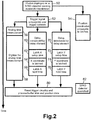
- delay elements 40 , 42 are provided to delay propagation of the trigger signal to the latches 20 , 22 by an amount effective to ensure that the latches 20 , 22 upon latching store the position coordinates of the SPAD detector 14 whose break down caused the trigger circuitry 34 to generate the trigger signal.
- two delay elements 40 , 42 are shown in illustrative FIGURE 2 to provide delays for respective latches 20 , 22 , depending upon the physical layout of the trigger circuitry it may be possible to use as few as a single delay element (for example, a delay element after which the transmission line breaks off to feed the row and column latches).
- a photon impinges upon a SPAD detector 14 of the detector array 12 causing avalanche breakdown of that SPAD detector 14.
- This breakdown causes two distinct results.
- the breakdown causes the trigger circuitry 34 to generate and propagate a trigger signal.
- the breakdown causes the position coordinates of the SPAD detector 14 that undergoes breakdown to propagate via the logical "OR" connections to the respective column and row latches 20 , 22.
- the trigger signal in turn causes three causal result event chains.
- the trigger signal propagates to the TDC circuitry 28 where it causes the TDC circuitry 28 to generate a time stamp.
- the time stamping operation entails two sub-operations: an analog time measurement 56 and a digitization operation 58 via which the analog time measurement is digitized to generate the digital time stamp.
- the analog time measurement 56 can utilize any event time measurement technique, such as a delay transmission line, a ring oscillator, or so forth.
- the digitization operation 58 digitizes the analog time measurement. Typically, the analog time measurement provides the fine time measurement providing high time resolution.
- the digitization operation 58 in some embodiments adds this fine (digitized) time measurement to the value of a digital clock (which provides coarse time measurement as compared with the transmission delay line, ring oscillator, or other fine analog time measurement) in order to generate a high resolution time stamp on the extended time scale of the digital clock.
- a second causal event chain caused by the trigger signal the column (i.e., X) position coordinate is latched by the column (X) latches 20 in response to the trigger signal.
- This causal event chain includes an optional initial delay 60 introduced by the optional delay element 40. In the timing shown in FIGURE 2 , the delay 60 ensures that the position coordinates propagation 54 to the latches 20 , 22 is completed before the latching operation which includes a setup time 62 preceding latching 64 of the column (X) latches 20 followed by a hold time 66.
- the setup and hold times 62 , 66 are determined by the design of the column latches 20 , and are the time interval preceding and succeeding the latching operation during which the values stored in the latches 20 should be stable in order to ensure integrity of the latching operation 64.
- a third causal event chain caused by the trigger signal the row (i.e., Y) position coordinate is latched by the row (Y) latches 22 in response to the trigger signal.
- This causal event chain includes an optional initial delay 70 introduced by the optional delay element 42.
- the delay 70 ensures that the position coordinates propagation 54 to the latches 20 , 22 is completed before the latching operation which includes a setup time 72 preceding latching 74 of the row (Y) latches 22 followed by a hold time 76.
- the setup and hold times 72 , 76 are determined by the design of the row latches 22, and are the time interval preceding and succeeding the latching operation during which the values stored in the latches 22 should be stable in order to ensure integrity of the latching operation 74.
- FIGURE 2 shows the row and column latching causal event chains as being identical in terms of time durations, it is also contemplated for the row and column latching causal event chains to have somewhat different timing characteristics.
- a diagrammatic operation 80 shown in FIGURE 2 collectively indicates operations entailed in completing the photon detection processing and output.
- the operation 80 includes resetting the trigger circuitry 34 (performed by the reset circuitry 26 diagrammatically shown in FIGURE 1 ) and processing and buffering the time and position data for the photon detection event (performed by the time and position processing and output circuitry 30 diagrammatically shown in FIGURE 1 ).
- a quench time 82 is diagrammatically indicated in FIGURE 2 - this quench time indicates the time at which the avalanche diode of the SPAD detector returns to the nonconductive reverse biased state.
- the SPAD detector is again ready to detect another photon; however, at the quench time 82 the SPAD detector is also no longer in break down. Accordingly, the latching operations 62 , 64 , 66 , 72 , 74 , 76 must be completed prior to the quench time 82.
- the time stamp digitizing 58 and the completion operations 80 can be performed before and/or after the quench time 82.
- the analog time measurement 56 and the latching 62 , 64 , 66 , 72 , 74 , 76 is complete, the temporal and spatial resolution is achieved and the remaining data processing is not under aggressive time constraints imposed by the SPAD detector quenching.
- the timing for resetting the trigger circuitry 34 depends upon the operation of the trigger circuitry 34. If the trigger circuitry 34 generates the trigger signal responsive to a SPAD detector transitioning into break down, then it may be possible to reset the trigger circuitry 34 before the SPAD detector is quenched. On the other hand, if the trigger circuitry 34 generates the trigger signal responsive to a SPAD detector being in break down, then the trigger circuitry 34 cannot be reset until after the SPAD detector is quenched (that is, until after the quench time 82 shown in FIGURE 2 ).
- the reset portion of the completion operations 80 also includes unlatching the latches 20 , 22. This can generally be done any time after the latched position data are processed and buffered. In some illustrating examples the latches 20 , 22 may unlatch automatically, e.g. after the hold time 66 , 76 is complete. In other illustrating examples the reset circuitry 26 sends a signal to unlatch the latches 20 , 22. The reset portion of the completion operations 80 may optionally also include resetting the values stored in the latches 20 , 22 , for example by the reset circuitry 26 sending a suitable control signal to the latches 20 , 22.
- the values stored in the latches 20 , 22 may be reset automatically once the SPAD detector in break down is quenched (that is, at the quench time 82 ) because at that time the logical "OR" tied to the latches returns to the "false” or “off” or “deactivated” (et cetera) value indicating that none of the SPAD detectors in the logical "OR" combination are in break down.
- Operation of the photon detector 10 as described with reference to FIGURE 2 provides single photon counting capability with high spatial and temporal resolution. It is effective for applications in which the impinging photon flux is sufficiently low that the average time between successive incoming photons is longer than the time of the processing described with reference to FIGURE 2 .
- An occasional instance of two photons arriving together can be accommodated insofar as the consequence of such an event would be to set two column latches, or two row latches. Thus, this can be detected by the completion operations 80 and the data can be discarded or suitably adjusted.
- the impinging photon flux may be higher, at least over a time interval of interest, such that the processing described with reference to FIGURE 2 cannot be completed during the interval between successive photon detection events.
- a situation may arise, for example, when the photon detector 10 is used in conjunction with a scintillator which generates a short burst of photons (i.e., a scintillation event) responsive to a radiation particle being detected by the scintillator.
- Another application example is imaging under light conditions which are of low intensity, but not so low as to employ the approach of FIGURE 2 .
- FIGURE 3 For such higher photon flux applications another operating mode may be employed, whose timing is diagrammatically depicted in FIGURE 3 .
- the delays 60 , 70 are optionally included to ensure positional data is stored in the latches 20 , 22 before the latching 62 , 64 , 66 , 72 , 74 , 76 is performed.
- these delays 60 , 70 are replaced by a longer integration time delay 60i which is again suitably implemented by the delay elements 40 , 42. Said another way, the delay time 60i introduced by the delay elements 40 , 42 is longer in the embodiment of FIGURE 3 , so as to provide an integration time.
- the same delay time 60i is also advantageous for the same delay time 60i to be introduced by both delay elements 40, 42 so that the row and column position data are integrated for the same time 60i. (As previously mentioned, in some contemplated embodiments this is achieved by constructing the delay elements 40 , 42 for the respective column and row latches 20 , 22 as a single delay element with the latching signal branching out from that single delay element to both sets of latches 20 , 22 .)
- the delay time 60i is chosen to provide an integration time over which position data for photon detection events is accumulated.
- the incoming flux of photons is sufficiently high that more than one photon will impinge upon the detector array 12 during the integration time 60i.
- Each photon detection event will cause the SPAD detector 14 that detects the photon to enter breakdown and load its position data into the latches 20 , 22.
- the latching 62 , 64 , 66 , 72 , 74 , 76 is performed as already described with reference to FIGURE 2 , so as to latch the position data for the photon detection events.
- the operations 56 , 58 operate as described with reference to FIGURE 2 , but triggered only by the first photon detection event so that the resulting digital timestamp will be for the first photon detection event.
- the position data stored in the latches 20 , 22 should be retained until the latching occurs. This will occur naturally if the quench time 82 occurs after the end of the integration time 60i (as shown in the embodiment of illustrative FIGURE 3 ), since in that case the avalanche diodes that are in breakdown will not yet have quenched at the time of latching. On the other hand, if the quench time is shorter than the integration time 60i then the latches 20 , 22 should be of a type that holds the "true" or "on” or “activated” (et cetera) value and does not reset upon quenching of the SPAD detector.
- the latch should follow a 0 ⁇ 1 transition but should not follow a 1 ⁇ 0 transition). In this case the latch will not go back to "false” or "off” or “deactivated” upon quenching of the avalanche diode. (Note that such a latch can also be used in the illustrating example of FIGURE 2 , but whenever such a latch is used the reset portion of the completion operations 80 should include resetting the values stored in the latches 20, 22 ) .
- the completion circuitry 80 processes the data to generate useful positional information. In some embodiments, this entails determining the (X,Y) coordinates for each photon detection event, thus producing a "map" of these events. In other embodiments the completion circuitry 80 processes the data to generate some statistical aggregation of the photon detection events, such as a center measurement (e.g., centroid or barycenter) of the set of photon detection events and/or a width measurement (e.g., a spatial full-width-at-half-maximum or FWHM, or a maximum spread).
- a center measurement e.g., centroid or barycenter
- a width measurement e.g., a spatial full-width-at-half-maximum or FWHM, or a maximum spread.
- the completion circuitry 80 may be unable to completely disambiguate positional data for multiple photon detection events. For example, if column latches X1 and X2 are "on" and row latches Y1 and Y2 are on, this could correspond to any of the following photon detection event sets: [(X1,Y2) and (X2,Y1)], or [(X1,Y1) and (X2,Y2)], or [(X1,Y2) and (X2,Y1) and either or both of (X1,Y1) and/or (X2,Y2)], or [(X1,Y1) and (X2,Y2) and either or both of (X1,Y2) and/or (X2,Y1)].
- This ambiguous situation may be addressable in the completion circuitry 80 by suitable approximate processing, e.g. randomly selecting two or three SPAD detectors of the ambiguous 2 ⁇ 2 SPAD detectors square as being the locations of photon detection events.
- the approach of FIGURE 3 is expected to be most effective (in the sense of avoiding the aforementioned ambiguity) if the integration time 60i and the incident photon flux are such that the distribution of photon detection events over the detector array 12 is sparse, meaning that there are few (if any) occurrences of two or more photon detection events along any single row or column.
- Another approach for more accurately disambiguating the positional data is to sample the rows and columns of the detector array 12 by latching these data at high speed into storage elements (not shown) such as switched capacitors or transmission gates, with the latching being initiated by the trigger signal generated by the trigger circuitry 34. If the sampling is fast enough (as compared with the average rate of photon detection events), then the time when a line changed its state is recorded, and the recorded time can be used to correlate row and column positions as well as to determine the time of arrival of the photon relative to the trigger signal.
- ambiguity due to multiple photon detection events is also possible in the operational mode of FIGURE 2 , and could occur if one or more additional photons are detected between the time of the events 50 , 52 and the end of the delay 60 , 70.
- these delays 60 , 70 are short, which reduces the likelihood of detecting multiple photons.
- the operational mode of FIGURE 2 is typically employed in low incident photon flux applications. Nonetheless, such an ambiguous situation, if it were to occur in the operational mode of FIGURE 2 , is readily detected as the completion circuitry 80 would detect two or more rows and/or two or more columns whose corresponding latches store the "true" or "on” or “activated” (et cetera) value.
- the processing and output circuitry 30 are suitably configured to output an error signal responsive to the latches (after latching responsive to a trigger signal generated by the trigger circuitry 34 ) indicating two or more SPAD detectors being in break down.
- the disclosed photon detector 10 provides both high spatial and high temporal resolution.
- high temporal resolution may not be needed or practically achievable.
- the time stamp generated by the process 56 , 58 corresponds to the beginning of the integration time 60i.
- the temporal resolution is thus limited by the integration time 60i , and it is not useful for the time resolution of the digital time stamp to be substantially finer than the integration time 60i.
- the processing 56 , 58 may optionally be omitted, and the TDC circuitry 28 reduced to simply recording the current clock cycle (for example) of the acquired photon detection events data.
- the TDC circuitry 28 may be omitted entirely, and the time stamping may be performed "off-chip" by assigning a time stamp to the data as it is communicated off the silicon chip or substrate 16.
- the disclosed photon detectors find diverse application in physics, astronomy, radiological imaging such as positron emission tomography (PET) or single-photon emission tomography (SPECT), or so forth.
- PET positron emission tomography
- SPECT single-photon emission tomography
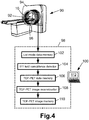
- a positron emission tomography (PET) imaging application is diagrammatically shown as an illustrative example.
- a PET scanner 90 includes a plurality of the disclosed photon detectors 10 arranged as a ring encircling a region of interest 92.
- the PET detector ring is suitably mounted on a housing or gantry 94 , and a scintillator ring 96 is disposed inside of the ring of photon detectors 10 such that a 511 keV particle emanating from a PET imaging subject disposed in the region of interest 92 is absorbed by the scintillator ring 96 to generate a burst (i.e., scintillation) of photons that is detected by the proximate photon detector 10.
- a burst i.e., scintillation
- the integration operational mode of FIGURE 3 is likely to be most useful, although it is also contemplated to employ the operational mode of FIGURE 2 in conjunction with a thin scintillator having a low photon yield (e.g., emitting only one or a few photons in each 511 keV scintillation).
- a thin scintillator having a low photon yield e.g., emitting only one or a few photons in each 511 keV scintillation.
- the resulting PET data are processed by an electronic processing device 98 , for example embodied as a suitably programmed computer 100.
- the photon detection events (or a center of a map of photon detection events determined in the operational mode of FIGURE 3 ) together with the digital time stamp and the particle energy (estimated from the number of photons detected during the integration time 60i ) forms list mode PET data that are stored in a list mode data memory 102.
- a 511 keV coincidence detector 104 identifies coincident 511 keV detection events in the list mode data using suitable temporal and energy windowing.
- Each pair of coincident 511 keV detection events defines a line of response (LOR), and the sourcing electron-hole annihilation event can be localized along the LOR using the time stamp as time-of-flight (TOF) data.
- the TOF-PET data are stored in a memory 106 , and are reconstructed by a suitable PET imaging data reconstruction processor 108 to form a reconstructed image that is suitably stored in a memory 110 , displayed on a display 112 of the computer 100 , or otherwise utilized.
- FIGURE 4 illustrates a PET application
- the disclosed photon detectors may be used in conjunction with a radiological imaging system, such as the illustrative PET scanner 90 , or as the photon detector of a radiation detector head of a gamma camera that is mounted on a robotic arm or gantry configured to orbit the radiation detector head around a region of interest, or so forth.
- a radiological imaging system such as the illustrative PET scanner 90
- the photon detector of a radiation detector head of a gamma camera that is mounted on a robotic arm or gantry configured to orbit the radiation detector head around a region of interest, or so forth.
Claims (11)
- Appareil comprenant :un détecteur de photons (10) comprenant :dans lequel les circuits à verrouillage (20, 22) comprennent :un réseau de détecteurs (12) comprenant des détecteurs (14) à diode à avalanche à photon unique (SPAD) conçus pour tomber en panne en réponse à un impact d'un photon,un circuit déclencheur (34) conçu pour générer un signal de déclenchement sensible à la panne d'un détecteur SPAD du réseau de détecteurs,des circuits à verrouillage (20, 22) conçus pour mémoriser des coordonnées de position des détecteurs SPAD du réseau de détecteurs, lesquels sont en panne,lesdits circuits à verrouillage étant conçus pour être verrouillés en réponse à un signal de déclenchement généré par les circuits déclencheurs,caractérisé en ce quel'appareil comprend en outre au moins un élément de retard (40, 42), lequel retarde la propagation du signal de déclenchement aux circuits à verrouillage (20, 22) d'un intervalle temporel d'intégration (60i) dans lequel les données de position pour des événements de détection de photons sont accumulées, dans lequel lorsque l'intervalle temporel d'intégration (60i) est terminé, le verrouillage des circuits à verrouillage (20, 22) est effectué de telle sorte que les circuits à verrouillage (20, 22), après le verrouillage, fournissent des coordonnées de position pour les détecteurs SPAD (14), lesquels tombent en panne dans l'intervalle temporel d'intégration (60i),des circuits à verrouillage de rangée (22), dans lequel chaque circuit à verrouillage de rangée se connecte à une combinaison logique « OU » des détecteurs SPAD (14) d'une rangée correspondante du réseau de détecteurs (12) ; etcircuits à verrouillage de colonne (20) dans lequel chaque circuit à verrouillage de colonne se connecte à une combinaison logique « OU » des détecteurs SPAD (14) d'une colonne correspondante du réseau de détecteurs (12).
- Appareil selon la revendication 1, dans lequel le détecteur de photons (10), comprenant le réseau de détecteurs (12), le circuit déclencheur (34) et les circuits à verrouillage (20, 22), est disposé de manière monolithique sur un substrat en silicium (16).
- Appareil selon l'une quelconque des revendications 1 à 2, dans lequel le détecteur de photons (10) comprend en outre :
des circuits (28) de convertisseur temps-numérique (TDC) conçus pour générer un horodatage numérique pour un signal de déclenchement généré par les circuits déclencheurs (34). - Appareil selon la revendication 3, dans lequel le détecteur de photons (10) comprend en outre :
des circuits de traitement et de sortie (30), lesquels génèrent et produisent (1) une position de détection de photons comprenant les coordonnées de position d'un détecteur SPAD (14), lequel est en panne en fonction des valeurs mémorisées dans les circuits à verrouillage (20, 22) après le verrouillage en réponse à un signal de déclenchement généré par les circuits déclencheurs (34), et (2) un horodatage numérique généré par les circuits TDC (28) pour le signal de déclenchement, lequel a provoqué le verrouillage des circuits à verrouillage. - Appareil selon la revendication 4, dans lequel les circuits de traitement et de sortie (30) sont en outre conçus pour émettre un signal d'erreur en réponse aux circuits à verrouillage après le verrouillage indiquant qu'au moins deux détecteurs SPAD (14) sont en panne.
- Appareil selon l'une quelconque des revendications 1 à 5, comprenant en outre :
un scanner (90) de tomographie par émission de positions (TEP) comprenant une pluralité desdits détecteurs de photons (10) conçus sous la forme d'un anneau détecteur entourant une zone d'intérêt (92). - Procédé comprenant :la fourniture d'un réseau de détecteurs (12) comprenant des détecteurs (14) à diode à avalanche à photon unique (SPAD) conçus pour tomber en panne en réponse à l'impact d'un photon dans une position ;la fourniture des circuits à verrouillage (20, 22) conçus pour mémoriser les coordonnées de position d'un détecteur SPAD du réseau de détecteurs, lequel est en panne, dans lequel les circuits à verrouillage (20, 22) comprennent :circuits à verrouillage de rangée (22), dans lequel chaque circuit à verrouillage de rangée se connecte à une combinaison logique « OU » des détecteurs SPAD (14) d'une rangée correspondante du réseau de détecteurs (12) ;et circuits à verrouillage de colonne (20), dans lequel chaque circuit à verrouillage de colonne se connecte à une combinaison logique « OU » des détecteurs SPAD (14) d'une colonne correspondante du réseau de détecteurs (12) ;la génération (52) d'un signal de déclenchement en réponse à la panne (50) d'un détecteur SPAD du réseau de détecteurs ;le retard de la propagation du signal de déclenchement vers les circuits à verrouillage d'un temps d'intégration (60i) dans lequel les données de position pour les événements de détection de photons sont accumulées ;le verrouillage (62, 64, 66, 72, 74, 76) des circuits à verrouillage en réponse au signal de déclenchement, dans lequel le verrouillage des circuits à verrouillage (20, 22) est retardé de l'intervalle temporel d'intégration (60i) ; etaprès le verrouillage (62, 64, 66, 72, 74, 76), la lecture (30) des circuits à verrouillage (20, 22) pour générer une image des détecteurs SPAD (14) du réseau de détecteurs (12), lesquels sont tombés en panne dans l'intervalle d'intégration (60i).
- Procédé selon la revendication 7, comprenant en outre :
la réalisation (56, 58) d'une conversion temps-numérique déclenchée par le signal de déclenchement pour générer un horodatage pour la panne (50) du détecteur SPAD (14), dont la panne a provoqué la génération (52) du signal de déclenchement. - Appareil selon la revendication 1, comprenant en outre :
des circuits de traitement (30) conçus pour sortir des positions de détection des photons détectés dans le temps d'intégration en fonction des coordonnées de position mémorisées dans les circuits à verrouillage verrouillés. - Appareil selon la revendication 9, comprenant en outre :un scintillateur (96) vu par le détecteur de photons (10) pour détecter les photons de scintillation émis par le scintillateur en réponse à une particule de rayonnement absorbée par le scintillateur ;dans lequel les circuits de traitement (30) sont conçus pour calculer un emplacement de la détection de particules de rayonnement en tant que centre des positions de détection de sortie des photons détectés par le détecteur de photons dans le temps d'intégration (60i).
- Appareil selon la revendication 10, comprenant en outre :
un système d'imagerie radiologique (90), comprenant ledit scintillateur (96) et ledit détecteur de photons (10), conçu sous la forme (1) d'un anneau détecteur de rayonnement entourant une zone d'intérêt (92) et/ou (2) d'une tête du détecteur de rayonnement montée sur un bras robotique ou portique conçu pour or-biter la tête du détecteur de rayonnement autour d'une zone d'intérêt.
Applications Claiming Priority (2)
| Application Number | Priority Date | Filing Date | Title |
|---|---|---|---|
| US201161514504P | 2011-08-03 | 2011-08-03 | |
| PCT/IB2012/053837 WO2013018006A1 (fr) | 2011-08-03 | 2012-07-27 | Modes de lecture sensibles à la position pour des réseaux de photomultiplicateurs numériques en silicium |
Publications (2)
| Publication Number | Publication Date |
|---|---|
| EP2740262A1 EP2740262A1 (fr) | 2014-06-11 |
| EP2740262B1 true EP2740262B1 (fr) | 2020-09-09 |
Family
ID=47018283
Family Applications (1)
| Application Number | Title | Priority Date | Filing Date |
|---|---|---|---|
| EP12772430.0A Active EP2740262B1 (fr) | 2011-08-03 | 2012-07-27 | Modes de lecture sensibles à la position pour des réseaux de photomultiplicateurs numériques en silicium |
Country Status (7)
| Country | Link |
|---|---|
| US (1) | US9176241B2 (fr) |
| EP (1) | EP2740262B1 (fr) |
| JP (1) | JP6059722B2 (fr) |
| CN (1) | CN103733609B (fr) |
| MX (1) | MX2014001272A (fr) |
| RU (1) | RU2014107914A (fr) |
| WO (1) | WO2013018006A1 (fr) |
Families Citing this family (70)
| Publication number | Priority date | Publication date | Assignee | Title |
|---|---|---|---|---|
| GB201219781D0 (en) * | 2012-11-02 | 2012-12-19 | St Microelectronics Res & Dev | Improvements in time of flight pixel circuits |
| WO2014201286A1 (fr) | 2013-06-12 | 2014-12-18 | Popovic Milos A | Modulateur optique ayant un processus de fabrication standard |
| WO2015173530A2 (fr) * | 2014-05-16 | 2015-11-19 | Alain Iltis | Procédé pour améliorer la résolution en énergie de détecteurs de rayons gamma a scintillation; système, composant et application associes |
| US10204944B2 (en) * | 2014-06-09 | 2019-02-12 | Kiskeya Microsystems Llc | Readout architecture for event-driven pixels |
| US9568620B2 (en) | 2014-09-22 | 2017-02-14 | General Electric Company | Solid state photomultiplier |
| CN105816194B (zh) * | 2015-01-07 | 2018-12-04 | 苏州瑞派宁科技有限公司 | 一种探测器信号读出的通道复用方法 |
| US9995830B2 (en) | 2015-03-17 | 2018-06-12 | Koninklijke Philips N.V. | Scintillation event localization in a radiation particle detector |
| US9606245B1 (en) | 2015-03-24 | 2017-03-28 | The Research Foundation For The State University Of New York | Autonomous gamma, X-ray, and particle detector |
| JP6528042B2 (ja) | 2015-06-19 | 2019-06-12 | 国立研究開発法人産業技術総合研究所 | 光子検出装置及び光子検出方法 |
| CN105182396B (zh) | 2015-06-29 | 2018-04-24 | 苏州瑞派宁科技有限公司 | 一种探测器信号读出的通道复用方法 |
| WO2017058319A2 (fr) | 2015-06-30 | 2017-04-06 | Massachusetts Institute Of Technology | Photodétecteurs de silicium-germanium couplés à un guide d'ondes et procédés de fabrication associés |
| US11105974B2 (en) | 2015-06-30 | 2021-08-31 | Massachusetts Institute Of Technology | Waveguide-coupled silicon-germanium photodetectors and fabrication methods for same |
| JP6789251B2 (ja) * | 2015-07-08 | 2020-11-25 | ザ コモンウェルス オブ オーストラリアThe Commonwealth Of Australia | Spadアレイ構造及び動作方法 |
| US11131756B2 (en) | 2015-09-29 | 2021-09-28 | Qualcomm Incorporated | LIDAR system with reflected signal strength measurement |
| US10371835B2 (en) | 2016-01-11 | 2019-08-06 | General Electric Company | Microcell interconnection in silicon photomultipliers |
| EP3516692B1 (fr) | 2016-09-23 | 2022-02-16 | Apple Inc. | Réseau spad éclairé par l'arrière empilé |
| US10502830B2 (en) | 2016-10-13 | 2019-12-10 | Waymo Llc | Limitation of noise on light detectors using an aperture |
| CN106580359B (zh) * | 2016-12-02 | 2020-04-14 | 中国科学院深圳先进技术研究院 | 探测器信号处理方法及装置 |
| US20180164414A1 (en) * | 2016-12-13 | 2018-06-14 | Sensl Technologies Ltd. | LiDAR Apparatus |
| US10422862B2 (en) | 2016-12-13 | 2019-09-24 | Sensl Technologies Ltd. | LiDAR apparatus |
| US20180164412A1 (en) * | 2016-12-13 | 2018-06-14 | Sensl Technologies Ltd. | LiDAR Apparatus |
| WO2018140522A2 (fr) * | 2017-01-25 | 2018-08-02 | Apple Inc. | Détecteur spad ayant une sensibilité modulée |
| US10656251B1 (en) | 2017-01-25 | 2020-05-19 | Apple Inc. | Signal acquisition in a SPAD detector |
| US10962628B1 (en) | 2017-01-26 | 2021-03-30 | Apple Inc. | Spatial temporal weighting in a SPAD detector |
| GB201704203D0 (en) * | 2017-03-16 | 2017-05-03 | Pixquanta Ltd | An electromagnetic radiation detection device |
| US20180329064A1 (en) * | 2017-05-09 | 2018-11-15 | Stmicroelectronics (Grenoble 2) Sas | Method and apparatus for mapping column illumination to column detection in a time of flight (tof) system |
| JP6881074B2 (ja) | 2017-06-22 | 2021-06-02 | 株式会社デンソー | 光検出器 |
| EP3428574A1 (fr) * | 2017-07-11 | 2019-01-16 | Fondazione Bruno Kessler | Dispositif de mesure de distance et procédé de mesure de ladite distance |
| KR101938984B1 (ko) * | 2017-08-09 | 2019-04-10 | 연세대학교 산학협력단 | Spad 거리측정 센서 기반의 2단계 트래킹을 이용한 거리 측정 장치 및 방법 |
| WO2019060942A1 (fr) * | 2017-09-27 | 2019-04-04 | The Commonwealth Of Australia | Micropuce à réseau de détecteurs d'avalanche monophotonique (spad) neuromorphique |
| JP7021501B2 (ja) * | 2017-10-26 | 2022-02-17 | オムロン株式会社 | データ取得方法およびデータ取得装置 |
| CN108051843B (zh) * | 2017-10-30 | 2020-11-24 | 深圳先进技术研究院 | 一种pet探测器的位置编码方法及装置 |
| US10158038B1 (en) | 2018-05-17 | 2018-12-18 | Hi Llc | Fast-gated photodetector architectures comprising dual voltage sources with a switch configuration |
| US10340408B1 (en) | 2018-05-17 | 2019-07-02 | Hi Llc | Non-invasive wearable brain interface systems including a headgear and a plurality of self-contained photodetector units configured to removably attach to the headgear |
| US10515993B2 (en) | 2018-05-17 | 2019-12-24 | Hi Llc | Stacked photodetector assemblies |
| US10420498B1 (en) | 2018-06-20 | 2019-09-24 | Hi Llc | Spatial and temporal-based diffusive correlation spectroscopy systems and methods |
| US11213206B2 (en) | 2018-07-17 | 2022-01-04 | Hi Llc | Non-invasive measurement systems with single-photon counting camera |
| DE102018213819B3 (de) * | 2018-08-16 | 2019-11-07 | Fraunhofer-Gesellschaft zur Förderung der angewandten Forschung e.V. | Vorrichtung und Verfahren für TDC-Sharing bei laufzeitbasierter Distanzmessung |
| EP3627178B1 (fr) * | 2018-09-19 | 2022-04-20 | ams AG | Dispositif de détection, module de capteur, système d'imagerie et procédé de fonctionnement d'un dispositif de détection |
| WO2020106813A1 (fr) * | 2018-11-20 | 2020-05-28 | Sense Photonics, Inc. | Procédés et systèmes pour la fourniture de signaux stroboscopiques distribués spatialement |
| US11233966B1 (en) | 2018-11-29 | 2022-01-25 | Apple Inc. | Breakdown voltage monitoring for avalanche diodes |
| WO2020131148A1 (fr) | 2018-12-21 | 2020-06-25 | Hi Llc | Rétroaction biologique pour la perception et la modulation de l'état mental à l'aide d'un système et d'un procédé non invasifs d'interface cérébrale |
| AU2020268718A1 (en) | 2019-05-06 | 2021-11-25 | Hi Llc | Photodetector architectures for time-correlated single photon counting |
| US11081611B2 (en) | 2019-05-21 | 2021-08-03 | Hi Llc | Photodetector architectures for efficient fast-gating comprising a control system controlling a current drawn by an array of photodetectors with a single photon avalanche diode |
| WO2020247185A1 (fr) | 2019-06-06 | 2020-12-10 | Hi Llc | Systèmes de photodétecteurs avec architectures de convertisseur numérique de temps de faible puissance |
| CN110389141B (zh) * | 2019-07-19 | 2022-04-05 | 东软医疗系统股份有限公司 | 位置读出设备、方法及装置 |
| CN110411577B (zh) * | 2019-07-23 | 2020-08-11 | 杭州电子科技大学 | Spad探测器阵列的异步读出电路及其异步读出方法 |
| US11378663B2 (en) | 2019-11-26 | 2022-07-05 | Waymo Llc | Systems and methods for biasing light detectors |
| CN113274043A (zh) * | 2020-01-31 | 2021-08-20 | 佳能医疗系统株式会社 | 放射线诊断装置及放射线诊断方法 |
| ES2849224B2 (es) | 2020-02-14 | 2022-01-21 | Consejo Superior Investigacion | Fotomultiplicador digital de combinacion or de pulsos |
| WO2021167877A1 (fr) | 2020-02-21 | 2021-08-26 | Hi Llc | Systèmes et procédés de mesure multimodaux pouvant être portés |
| US11950879B2 (en) | 2020-02-21 | 2024-04-09 | Hi Llc | Estimation of source-detector separation in an optical measurement system |
| US11096620B1 (en) | 2020-02-21 | 2021-08-24 | Hi Llc | Wearable module assemblies for an optical measurement system |
| US11630310B2 (en) | 2020-02-21 | 2023-04-18 | Hi Llc | Wearable devices and wearable assemblies with adjustable positioning for use in an optical measurement system |
| WO2021167876A1 (fr) | 2020-02-21 | 2021-08-26 | Hi Llc | Procédés et systèmes permettant d'initier et de mener une étude personnalisée de recherche cérébrale activée par ordinateur |
| WO2021167893A1 (fr) | 2020-02-21 | 2021-08-26 | Hi Llc | Ensembles détecteurs intégrés pour un module pouvant être porté d'un système de mesure optique |
| WO2021188496A1 (fr) | 2020-03-20 | 2021-09-23 | Hi Llc | Étalonnage de photodétecteur d'un système de mesure optique |
| US11857348B2 (en) | 2020-03-20 | 2024-01-02 | Hi Llc | Techniques for determining a timing uncertainty of a component of an optical measurement system |
| US11864867B2 (en) | 2020-03-20 | 2024-01-09 | Hi Llc | Control circuit for a light source in an optical measurement system by applying voltage with a first polarity to start an emission of a light pulse and applying voltage with a second polarity to stop the emission of the light pulse |
| US11819311B2 (en) | 2020-03-20 | 2023-11-21 | Hi Llc | Maintaining consistent photodetector sensitivity in an optical measurement system |
| US11877825B2 (en) | 2020-03-20 | 2024-01-23 | Hi Llc | Device enumeration in an optical measurement system |
| US11645483B2 (en) | 2020-03-20 | 2023-05-09 | Hi Llc | Phase lock loop circuit based adjustment of a measurement time window in an optical measurement system |
| US11245404B2 (en) | 2020-03-20 | 2022-02-08 | Hi Llc | Phase lock loop circuit based signal generation in an optical measurement system |
| US11607132B2 (en) | 2020-03-20 | 2023-03-21 | Hi Llc | Temporal resolution control for temporal point spread function generation in an optical measurement system |
| US11187575B2 (en) | 2020-03-20 | 2021-11-30 | Hi Llc | High density optical measurement systems with minimal number of light sources |
| US11476372B1 (en) | 2020-05-13 | 2022-10-18 | Apple Inc. | SPAD-based photon detectors with multi-phase sampling TDCs |
| BE1028366B1 (nl) * | 2020-05-29 | 2022-01-11 | Voxelsensors Srl | Pixel sensor systeem |
| CN115413320A (zh) | 2020-05-29 | 2022-11-29 | 体素传感器有限责任公司 | 像素传感器系统 |
| US11555901B2 (en) * | 2020-07-27 | 2023-01-17 | Nxp B.V. | Photon-based detection using single-channel time-to-digital conversion |
| EP4125269A1 (fr) * | 2021-07-29 | 2023-02-01 | Leica Microsystems CMS GmbH | Réseau de détecteur, système d'imagerie et procédé d'imagerie d'un échantillon |
Family Cites Families (26)
| Publication number | Priority date | Publication date | Assignee | Title |
|---|---|---|---|---|
| US4672207A (en) * | 1985-08-21 | 1987-06-09 | The United States Of America As Represented By The United States Department Of Energy | Readout system for multi-crystal gamma cameras |
| US5099128A (en) | 1989-03-17 | 1992-03-24 | Roger Stettner | High resolution position sensitive detector |
| US5619040A (en) | 1994-03-29 | 1997-04-08 | Shapiro; Stephen L. | Data acquisition system |
| EP1521982A1 (fr) | 2002-07-17 | 2005-04-13 | European Organization for Nuclear Research | Detecteur de rayons gamma pour tomographie par emission de positrons (tep) et tomographie d'emission monophotonique (tem) |
| US7547872B2 (en) | 2005-02-14 | 2009-06-16 | Ecole Polytechnique Federale De Lausanne | Integrated circuit comprising an array of single photon avalanche diodes |
| EP1875273B1 (fr) * | 2005-04-22 | 2011-11-16 | Koninklijke Philips Electronics N.V. | Scanneur a tomographie par emission de positons/resonance magnetique avec fonction de temps de vol |
| EP1922564B1 (fr) | 2005-08-26 | 2011-12-14 | Koninklijke Philips Electronics N.V. | Detecteur d'imagerie medicale a resolution elevee |
| WO2007127607A1 (fr) | 2006-04-25 | 2007-11-08 | Koninklijke Philips Electronics, N.V. | Implementation de photodiodes a avalanche dans des procedes bi-cmos |
| JP5421102B2 (ja) * | 2006-07-28 | 2014-02-19 | コーニンクレッカ フィリップス エヌ ヴェ | 陽電子放出型断層撮影における飛行時間測定 |
| JP2008096278A (ja) | 2006-10-12 | 2008-04-24 | Fujifilm Corp | 放射線画像検出器 |
| US8259293B2 (en) | 2007-03-15 | 2012-09-04 | Johns Hopkins University | Deep submicron and nano CMOS single photon photodetector pixel with event based circuits for readout data-rate reduction communication system |
| US9087755B2 (en) | 2007-04-24 | 2015-07-21 | Koninklijke Philips N.V. | Photodiodes and fabrication thereof |
| CN101680953B (zh) | 2007-05-16 | 2014-08-13 | 皇家飞利浦电子股份有限公司 | 虚拟pet探测器和用于pet的准像素化读出方案 |
| EP2160615B1 (fr) | 2007-06-25 | 2011-05-18 | Koninklijke Philips Electronics N.V. | Autotest de photodiode |
| WO2009019659A2 (fr) | 2007-08-08 | 2009-02-12 | Koninklijke Philips Electronics N.V. | Circuit de lecture de photomultiplicateur au silicium |
| WO2009031074A2 (fr) | 2007-09-04 | 2009-03-12 | Koninklijke Philips Electronics N.V. | Résolution d'énergie de photomultiplicateur au silicium |
| WO2009054070A1 (fr) * | 2007-10-26 | 2009-04-30 | Shimadzu Corporation | Détecteur de rayonnement |
| EP2257835B1 (fr) | 2008-03-19 | 2019-07-31 | Koninklijke Philips N.V. | Détecteur de rayonnement de photon unique |
| CN102246058B (zh) | 2008-12-15 | 2014-06-11 | 皇家飞利浦电子股份有限公司 | 用于硅光电倍增管和其他单光子计数器的温度补偿电路 |
| EP2380038B1 (fr) | 2008-12-22 | 2019-01-09 | Koninklijke Philips N.V. | Capteur d'image cmos |
| CN102388321B (zh) | 2008-12-22 | 2014-10-22 | 皇家飞利浦电子股份有限公司 | 高动态范围光传感器 |
| KR101111011B1 (ko) | 2008-12-26 | 2012-02-15 | 연세대학교 산학협력단 | 감마선 영상측정을 위한 다층 평판형 검출기 및 3차원 위치검출방법 |
| JP2010249672A (ja) | 2009-04-16 | 2010-11-04 | Toshiba Corp | ポジトロンct装置 |
| RU2550581C2 (ru) | 2009-05-28 | 2015-05-10 | Конинклейке Филипс Электроникс Н.В. | Способ улучшения временного разрешения цифровых кремниевых фотоумножителей |
| WO2010149593A1 (fr) * | 2009-06-22 | 2010-12-29 | Toyota Motor Europe Nv/Sa | Télémètre optique à lumière pulsée |
| TWI559763B (zh) * | 2009-10-01 | 2016-11-21 | 索尼半導體解決方案公司 | 影像取得裝置及照相機系統 |
-
2012
- 2012-07-27 RU RU2014107914/28A patent/RU2014107914A/ru not_active Application Discontinuation
- 2012-07-27 EP EP12772430.0A patent/EP2740262B1/fr active Active
- 2012-07-27 WO PCT/IB2012/053837 patent/WO2013018006A1/fr active Application Filing
- 2012-07-27 US US14/234,650 patent/US9176241B2/en active Active
- 2012-07-27 CN CN201280038184.XA patent/CN103733609B/zh active Active
- 2012-07-27 JP JP2014523426A patent/JP6059722B2/ja active Active
- 2012-07-27 MX MX2014001272A patent/MX2014001272A/es not_active Application Discontinuation
Non-Patent Citations (1)
| Title |
|---|
| None * |
Also Published As
| Publication number | Publication date |
|---|---|
| JP2014529923A (ja) | 2014-11-13 |
| MX2014001272A (es) | 2014-05-19 |
| CN103733609A (zh) | 2014-04-16 |
| CN103733609B (zh) | 2017-07-11 |
| US20140175294A1 (en) | 2014-06-26 |
| JP6059722B2 (ja) | 2017-01-11 |
| WO2013018006A1 (fr) | 2013-02-07 |
| US9176241B2 (en) | 2015-11-03 |
| EP2740262A1 (fr) | 2014-06-11 |
| RU2014107914A (ru) | 2015-09-10 |
Similar Documents
| Publication | Publication Date | Title |
|---|---|---|
| EP2740262B1 (fr) | Modes de lecture sensibles à la position pour des réseaux de photomultiplicateurs numériques en silicium | |
| US10656288B2 (en) | Digital silicon photomultiplier for TOF-PET | |
| Braga et al. | A Fully Digital 8$\,\times\, $16 SiPM Array for PET Applications With Per-Pixel TDCs and Real-Time Energy Output | |
| JP6325650B2 (ja) | 光検出器画素アレイを有する放射線検出装置、pet撮像システム、光フォトン加算方法、及び光フォトン加算方法のステップを実行するためのコンピュータプログラム | |
| US8723132B2 (en) | Single photon radiation detector | |
| Fishburn et al. | System tradeoffs in gamma-ray detection utilizing SPAD arrays and scintillators | |
| JP2018530176A (ja) | Spadアレイ構造及び動作方法 | |
| Braga et al. | An 8× 16-pixel 92kSPAD time-resolved sensor with on-pixel 64ps 12b TDC and 100MS/s real-time energy histogramming in 0.13 µm CIS technology for PET/MRI applications | |
| US9541448B2 (en) | Silicon photomultipliers with digitized micro-cells having a first one-shot pulse and a second one-shot pulse provided by an electronic circuit | |
| Mandai et al. | A $780\times 800~{\mu}\hbox {m}^ 2$ Multichannel Digital Silicon Photomultiplier With Column-Parallel Time-to-Digital Converter and Basic Characterization | |
| US20220206158A1 (en) | Event driven shared memory pixel | |
| Pozas-Flores et al. | Design of a smart SiPM based on focal-plane processing elements for improved spatial resolution in PET | |
| US11906354B2 (en) | Recharge circuit for digital silicon photomultipliers | |
| Bandi | Design of CMOS Digital Silicon Photomultipliers with TOF for Positron Emission Tomography | |
| Mandai | Multichannel Digital Silicon Photomultiplier for Time-of-Flight PET | |
| Yang et al. | A spad array sensor based on breakdown pixel extraction architecture with background readout for scintillation detector |
Legal Events
| Date | Code | Title | Description |
|---|---|---|---|
| PUAI | Public reference made under article 153(3) epc to a published international application that has entered the european phase |
Free format text: ORIGINAL CODE: 0009012 |
|
| 17P | Request for examination filed |
Effective date: 20140303 |
|
| AK | Designated contracting states |
Kind code of ref document: A1 Designated state(s): AL AT BE BG CH CY CZ DE DK EE ES FI FR GB GR HR HU IE IS IT LI LT LU LV MC MK MT NL NO PL PT RO RS SE SI SK SM TR |
|
| DAX | Request for extension of the european patent (deleted) | ||
| STAA | Information on the status of an ep patent application or granted ep patent |
Free format text: STATUS: EXAMINATION IS IN PROGRESS |
|
| 17Q | First examination report despatched |
Effective date: 20180710 |
|
| RAP1 | Party data changed (applicant data changed or rights of an application transferred) |
Owner name: PHILIPS GMBH Owner name: KONINKLIJKE PHILIPS N.V. |
|
| GRAP | Despatch of communication of intention to grant a patent |
Free format text: ORIGINAL CODE: EPIDOSNIGR1 |
|
| STAA | Information on the status of an ep patent application or granted ep patent |
Free format text: STATUS: GRANT OF PATENT IS INTENDED |
|
| RAP1 | Party data changed (applicant data changed or rights of an application transferred) |
Owner name: KONINKLIJKE PHILIPS N.V. Owner name: PHILIPS GMBH |
|
| INTG | Intention to grant announced |
Effective date: 20200318 |
|
| GRAS | Grant fee paid |
Free format text: ORIGINAL CODE: EPIDOSNIGR3 |
|
| GRAA | (expected) grant |
Free format text: ORIGINAL CODE: 0009210 |
|
| STAA | Information on the status of an ep patent application or granted ep patent |
Free format text: STATUS: THE PATENT HAS BEEN GRANTED |
|
| AK | Designated contracting states |
Kind code of ref document: B1 Designated state(s): AL AT BE BG CH CY CZ DE DK EE ES FI FR GB GR HR HU IE IS IT LI LT LU LV MC MK MT NL NO PL PT RO RS SE SI SK SM TR |
|
| REG | Reference to a national code |
Ref country code: GB Ref legal event code: FG4D |
|
| REG | Reference to a national code |
Ref country code: AT Ref legal event code: REF Ref document number: 1313030 Country of ref document: AT Kind code of ref document: T Effective date: 20200915 Ref country code: CH Ref legal event code: EP |
|
| REG | Reference to a national code |
Ref country code: IE Ref legal event code: FG4D |
|
| REG | Reference to a national code |
Ref country code: DE Ref legal event code: R096 Ref document number: 602012072249 Country of ref document: DE |
|
| REG | Reference to a national code |
Ref country code: DE Ref legal event code: R081 Ref document number: 602012072249 Country of ref document: DE Owner name: PHILIPS GMBH, DE Free format text: FORMER OWNER: PHILIPS GMBH, 20099 HAMBURG, DE |
|
| REG | Reference to a national code |
Ref country code: LT Ref legal event code: MG4D |
|
| PG25 | Lapsed in a contracting state [announced via postgrant information from national office to epo] |
Ref country code: BG Free format text: LAPSE BECAUSE OF FAILURE TO SUBMIT A TRANSLATION OF THE DESCRIPTION OR TO PAY THE FEE WITHIN THE PRESCRIBED TIME-LIMIT Effective date: 20201209 Ref country code: GR Free format text: LAPSE BECAUSE OF FAILURE TO SUBMIT A TRANSLATION OF THE DESCRIPTION OR TO PAY THE FEE WITHIN THE PRESCRIBED TIME-LIMIT Effective date: 20201210 Ref country code: LT Free format text: LAPSE BECAUSE OF FAILURE TO SUBMIT A TRANSLATION OF THE DESCRIPTION OR TO PAY THE FEE WITHIN THE PRESCRIBED TIME-LIMIT Effective date: 20200909 Ref country code: HR Free format text: LAPSE BECAUSE OF FAILURE TO SUBMIT A TRANSLATION OF THE DESCRIPTION OR TO PAY THE FEE WITHIN THE PRESCRIBED TIME-LIMIT Effective date: 20200909 Ref country code: NO Free format text: LAPSE BECAUSE OF FAILURE TO SUBMIT A TRANSLATION OF THE DESCRIPTION OR TO PAY THE FEE WITHIN THE PRESCRIBED TIME-LIMIT Effective date: 20201209 Ref country code: SE Free format text: LAPSE BECAUSE OF FAILURE TO SUBMIT A TRANSLATION OF THE DESCRIPTION OR TO PAY THE FEE WITHIN THE PRESCRIBED TIME-LIMIT Effective date: 20200909 Ref country code: FI Free format text: LAPSE BECAUSE OF FAILURE TO SUBMIT A TRANSLATION OF THE DESCRIPTION OR TO PAY THE FEE WITHIN THE PRESCRIBED TIME-LIMIT Effective date: 20200909 |
|
| REG | Reference to a national code |
Ref country code: AT Ref legal event code: MK05 Ref document number: 1313030 Country of ref document: AT Kind code of ref document: T Effective date: 20200909 |
|
| REG | Reference to a national code |
Ref country code: NL Ref legal event code: MP Effective date: 20200909 |
|
| PG25 | Lapsed in a contracting state [announced via postgrant information from national office to epo] |
Ref country code: RS Free format text: LAPSE BECAUSE OF FAILURE TO SUBMIT A TRANSLATION OF THE DESCRIPTION OR TO PAY THE FEE WITHIN THE PRESCRIBED TIME-LIMIT Effective date: 20200909 Ref country code: PL Free format text: LAPSE BECAUSE OF FAILURE TO SUBMIT A TRANSLATION OF THE DESCRIPTION OR TO PAY THE FEE WITHIN THE PRESCRIBED TIME-LIMIT Effective date: 20200909 Ref country code: LV Free format text: LAPSE BECAUSE OF FAILURE TO SUBMIT A TRANSLATION OF THE DESCRIPTION OR TO PAY THE FEE WITHIN THE PRESCRIBED TIME-LIMIT Effective date: 20200909 |
|
| PG25 | Lapsed in a contracting state [announced via postgrant information from national office to epo] |
Ref country code: EE Free format text: LAPSE BECAUSE OF FAILURE TO SUBMIT A TRANSLATION OF THE DESCRIPTION OR TO PAY THE FEE WITHIN THE PRESCRIBED TIME-LIMIT Effective date: 20200909 Ref country code: CZ Free format text: LAPSE BECAUSE OF FAILURE TO SUBMIT A TRANSLATION OF THE DESCRIPTION OR TO PAY THE FEE WITHIN THE PRESCRIBED TIME-LIMIT Effective date: 20200909 Ref country code: NL Free format text: LAPSE BECAUSE OF FAILURE TO SUBMIT A TRANSLATION OF THE DESCRIPTION OR TO PAY THE FEE WITHIN THE PRESCRIBED TIME-LIMIT Effective date: 20200909 Ref country code: PT Free format text: LAPSE BECAUSE OF FAILURE TO SUBMIT A TRANSLATION OF THE DESCRIPTION OR TO PAY THE FEE WITHIN THE PRESCRIBED TIME-LIMIT Effective date: 20210111 Ref country code: RO Free format text: LAPSE BECAUSE OF FAILURE TO SUBMIT A TRANSLATION OF THE DESCRIPTION OR TO PAY THE FEE WITHIN THE PRESCRIBED TIME-LIMIT Effective date: 20200909 Ref country code: SM Free format text: LAPSE BECAUSE OF FAILURE TO SUBMIT A TRANSLATION OF THE DESCRIPTION OR TO PAY THE FEE WITHIN THE PRESCRIBED TIME-LIMIT Effective date: 20200909 |
|
| PG25 | Lapsed in a contracting state [announced via postgrant information from national office to epo] |
Ref country code: IS Free format text: LAPSE BECAUSE OF FAILURE TO SUBMIT A TRANSLATION OF THE DESCRIPTION OR TO PAY THE FEE WITHIN THE PRESCRIBED TIME-LIMIT Effective date: 20210109 Ref country code: ES Free format text: LAPSE BECAUSE OF FAILURE TO SUBMIT A TRANSLATION OF THE DESCRIPTION OR TO PAY THE FEE WITHIN THE PRESCRIBED TIME-LIMIT Effective date: 20200909 Ref country code: AL Free format text: LAPSE BECAUSE OF FAILURE TO SUBMIT A TRANSLATION OF THE DESCRIPTION OR TO PAY THE FEE WITHIN THE PRESCRIBED TIME-LIMIT Effective date: 20200909 Ref country code: AT Free format text: LAPSE BECAUSE OF FAILURE TO SUBMIT A TRANSLATION OF THE DESCRIPTION OR TO PAY THE FEE WITHIN THE PRESCRIBED TIME-LIMIT Effective date: 20200909 |
|
| REG | Reference to a national code |
Ref country code: DE Ref legal event code: R097 Ref document number: 602012072249 Country of ref document: DE |
|
| PG25 | Lapsed in a contracting state [announced via postgrant information from national office to epo] |
Ref country code: SK Free format text: LAPSE BECAUSE OF FAILURE TO SUBMIT A TRANSLATION OF THE DESCRIPTION OR TO PAY THE FEE WITHIN THE PRESCRIBED TIME-LIMIT Effective date: 20200909 |
|
| PLBE | No opposition filed within time limit |
Free format text: ORIGINAL CODE: 0009261 |
|
| STAA | Information on the status of an ep patent application or granted ep patent |
Free format text: STATUS: NO OPPOSITION FILED WITHIN TIME LIMIT |
|
| 26N | No opposition filed |
Effective date: 20210610 |
|
| PG25 | Lapsed in a contracting state [announced via postgrant information from national office to epo] |
Ref country code: DK Free format text: LAPSE BECAUSE OF FAILURE TO SUBMIT A TRANSLATION OF THE DESCRIPTION OR TO PAY THE FEE WITHIN THE PRESCRIBED TIME-LIMIT Effective date: 20200909 Ref country code: SI Free format text: LAPSE BECAUSE OF FAILURE TO SUBMIT A TRANSLATION OF THE DESCRIPTION OR TO PAY THE FEE WITHIN THE PRESCRIBED TIME-LIMIT Effective date: 20200909 |
|
| PG25 | Lapsed in a contracting state [announced via postgrant information from national office to epo] |
Ref country code: IT Free format text: LAPSE BECAUSE OF FAILURE TO SUBMIT A TRANSLATION OF THE DESCRIPTION OR TO PAY THE FEE WITHIN THE PRESCRIBED TIME-LIMIT Effective date: 20200909 |
|
| REG | Reference to a national code |
Ref country code: CH Ref legal event code: PL |
|
| GBPC | Gb: european patent ceased through non-payment of renewal fee |
Effective date: 20210727 |
|
| PG25 | Lapsed in a contracting state [announced via postgrant information from national office to epo] |
Ref country code: MC Free format text: LAPSE BECAUSE OF FAILURE TO SUBMIT A TRANSLATION OF THE DESCRIPTION OR TO PAY THE FEE WITHIN THE PRESCRIBED TIME-LIMIT Effective date: 20200909 |
|
| REG | Reference to a national code |
Ref country code: BE Ref legal event code: MM Effective date: 20210731 |
|
| PG25 | Lapsed in a contracting state [announced via postgrant information from national office to epo] |
Ref country code: LI Free format text: LAPSE BECAUSE OF NON-PAYMENT OF DUE FEES Effective date: 20210731 Ref country code: GB Free format text: LAPSE BECAUSE OF NON-PAYMENT OF DUE FEES Effective date: 20210727 Ref country code: CH Free format text: LAPSE BECAUSE OF NON-PAYMENT OF DUE FEES Effective date: 20210731 |
|
| PG25 | Lapsed in a contracting state [announced via postgrant information from national office to epo] |
Ref country code: LU Free format text: LAPSE BECAUSE OF NON-PAYMENT OF DUE FEES Effective date: 20210727 Ref country code: FR Free format text: LAPSE BECAUSE OF NON-PAYMENT OF DUE FEES Effective date: 20210731 |
|
| PG25 | Lapsed in a contracting state [announced via postgrant information from national office to epo] |
Ref country code: IE Free format text: LAPSE BECAUSE OF NON-PAYMENT OF DUE FEES Effective date: 20210727 Ref country code: BE Free format text: LAPSE BECAUSE OF NON-PAYMENT OF DUE FEES Effective date: 20210731 |
|
| REG | Reference to a national code |
Ref country code: DE Ref legal event code: R079 Ref document number: 602012072249 Country of ref document: DE Free format text: PREVIOUS MAIN CLASS: H04N0005369000 Ipc: H04N0025700000 |
|
| PG25 | Lapsed in a contracting state [announced via postgrant information from national office to epo] |
Ref country code: HU Free format text: LAPSE BECAUSE OF FAILURE TO SUBMIT A TRANSLATION OF THE DESCRIPTION OR TO PAY THE FEE WITHIN THE PRESCRIBED TIME-LIMIT; INVALID AB INITIO Effective date: 20120727 Ref country code: CY Free format text: LAPSE BECAUSE OF FAILURE TO SUBMIT A TRANSLATION OF THE DESCRIPTION OR TO PAY THE FEE WITHIN THE PRESCRIBED TIME-LIMIT Effective date: 20200909 |
|
| PGFP | Annual fee paid to national office [announced via postgrant information from national office to epo] |
Ref country code: DE Payment date: 20230726 Year of fee payment: 12 |
|
| REG | Reference to a national code |
Ref country code: DE Ref legal event code: R084 Ref document number: 602012072249 Country of ref document: DE |