EP2738802A1 - Heat dissipating component for semiconductor element - Google Patents
Heat dissipating component for semiconductor element Download PDFInfo
- Publication number
- EP2738802A1 EP2738802A1 EP12816956.2A EP12816956A EP2738802A1 EP 2738802 A1 EP2738802 A1 EP 2738802A1 EP 12816956 A EP12816956 A EP 12816956A EP 2738802 A1 EP2738802 A1 EP 2738802A1
- Authority
- EP
- European Patent Office
- Prior art keywords
- aluminum
- layer
- diamond
- composite
- heat dissipating
- Prior art date
- Legal status (The legal status is an assumption and is not a legal conclusion. Google has not performed a legal analysis and makes no representation as to the accuracy of the status listed.)
- Granted
Links
- 239000004065 semiconductor Substances 0.000 title claims abstract description 71
- 239000010432 diamond Substances 0.000 claims abstract description 213
- 229910003460 diamond Inorganic materials 0.000 claims abstract description 213
- 239000002131 composite material Substances 0.000 claims abstract description 185
- 229910052751 metal Inorganic materials 0.000 claims abstract description 88
- 239000002184 metal Substances 0.000 claims abstract description 88
- 239000000919 ceramic Substances 0.000 claims abstract description 59
- XAGFODPZIPBFFR-UHFFFAOYSA-N aluminium Chemical group [Al] XAGFODPZIPBFFR-UHFFFAOYSA-N 0.000 claims abstract description 48
- 229910052782 aluminium Inorganic materials 0.000 claims abstract description 47
- 229910000990 Ni alloy Inorganic materials 0.000 claims abstract description 38
- 239000002245 particle Substances 0.000 claims abstract description 32
- 238000007747 plating Methods 0.000 claims description 61
- 239000000835 fiber Substances 0.000 claims description 27
- 238000009716 squeeze casting Methods 0.000 claims description 23
- HBMJWWWQQXIZIP-UHFFFAOYSA-N silicon carbide Chemical compound [Si+]#[C-] HBMJWWWQQXIZIP-UHFFFAOYSA-N 0.000 claims description 16
- 229910010271 silicon carbide Inorganic materials 0.000 claims description 16
- 239000011701 zinc Substances 0.000 claims description 13
- 238000007772 electroless plating Methods 0.000 claims description 6
- 229910002601 GaN Inorganic materials 0.000 claims description 4
- 229910001218 Gallium arsenide Inorganic materials 0.000 claims description 4
- HCHKCACWOHOZIP-UHFFFAOYSA-N Zinc Chemical group [Zn] HCHKCACWOHOZIP-UHFFFAOYSA-N 0.000 claims description 4
- 238000006467 substitution reaction Methods 0.000 claims description 4
- 229910052725 zinc Inorganic materials 0.000 claims description 4
- 229910003465 moissanite Inorganic materials 0.000 claims 1
- 239000010410 layer Substances 0.000 abstract description 223
- 239000011247 coating layer Substances 0.000 abstract 1
- 239000000843 powder Substances 0.000 description 54
- 229910000838 Al alloy Inorganic materials 0.000 description 40
- 238000005336 cracking Methods 0.000 description 28
- 238000000034 method Methods 0.000 description 27
- 230000003746 surface roughness Effects 0.000 description 25
- 239000000463 material Substances 0.000 description 21
- 238000003754 machining Methods 0.000 description 18
- 238000012360 testing method Methods 0.000 description 14
- 239000006082 mold release agent Substances 0.000 description 13
- 238000005470 impregnation Methods 0.000 description 12
- 230000000052 comparative effect Effects 0.000 description 11
- 238000005498 polishing Methods 0.000 description 11
- OKTJSMMVPCPJKN-UHFFFAOYSA-N Carbon Chemical compound [C] OKTJSMMVPCPJKN-UHFFFAOYSA-N 0.000 description 10
- 229910002804 graphite Inorganic materials 0.000 description 10
- 239000010439 graphite Substances 0.000 description 10
- 239000011148 porous material Substances 0.000 description 10
- PNEYBMLMFCGWSK-UHFFFAOYSA-N aluminium oxide Inorganic materials [O-2].[O-2].[O-2].[Al+3].[Al+3] PNEYBMLMFCGWSK-UHFFFAOYSA-N 0.000 description 9
- 229910018104 Ni-P Inorganic materials 0.000 description 8
- 229910018536 Ni—P Inorganic materials 0.000 description 8
- 239000002344 surface layer Substances 0.000 description 8
- XUIMIQQOPSSXEZ-UHFFFAOYSA-N Silicon Chemical compound [Si] XUIMIQQOPSSXEZ-UHFFFAOYSA-N 0.000 description 7
- XEEYBQQBJWHFJM-UHFFFAOYSA-N Iron Chemical compound [Fe] XEEYBQQBJWHFJM-UHFFFAOYSA-N 0.000 description 6
- FYYHWMGAXLPEAU-UHFFFAOYSA-N Magnesium Chemical compound [Mg] FYYHWMGAXLPEAU-UHFFFAOYSA-N 0.000 description 6
- VYPSYNLAJGMNEJ-UHFFFAOYSA-N Silicium dioxide Chemical compound O=[Si]=O VYPSYNLAJGMNEJ-UHFFFAOYSA-N 0.000 description 6
- 230000000694 effects Effects 0.000 description 6
- 239000011888 foil Substances 0.000 description 6
- 238000010438 heat treatment Methods 0.000 description 6
- 229910052749 magnesium Inorganic materials 0.000 description 6
- 239000011777 magnesium Substances 0.000 description 6
- 238000005259 measurement Methods 0.000 description 6
- 239000000155 melt Substances 0.000 description 6
- 150000002739 metals Chemical class 0.000 description 6
- 229910052710 silicon Inorganic materials 0.000 description 6
- 239000010703 silicon Substances 0.000 description 6
- WZFUQSJFWNHZHM-UHFFFAOYSA-N 2-[4-[2-(2,3-dihydro-1H-inden-2-ylamino)pyrimidin-5-yl]piperazin-1-yl]-1-(2,4,6,7-tetrahydrotriazolo[4,5-c]pyridin-5-yl)ethanone Chemical compound C1C(CC2=CC=CC=C12)NC1=NC=C(C=N1)N1CCN(CC1)CC(=O)N1CC2=C(CC1)NN=N2 WZFUQSJFWNHZHM-UHFFFAOYSA-N 0.000 description 5
- 239000006061 abrasive grain Substances 0.000 description 5
- 229910045601 alloy Inorganic materials 0.000 description 5
- 239000000956 alloy Substances 0.000 description 5
- 238000000137 annealing Methods 0.000 description 5
- 238000005219 brazing Methods 0.000 description 5
- 239000010949 copper Substances 0.000 description 5
- RYGMFSIKBFXOCR-UHFFFAOYSA-N Copper Chemical compound [Cu] RYGMFSIKBFXOCR-UHFFFAOYSA-N 0.000 description 4
- 230000015572 biosynthetic process Effects 0.000 description 4
- 230000008859 change Effects 0.000 description 4
- 229910052802 copper Inorganic materials 0.000 description 4
- 238000000227 grinding Methods 0.000 description 4
- 238000004519 manufacturing process Methods 0.000 description 4
- 230000008569 process Effects 0.000 description 4
- 238000012545 processing Methods 0.000 description 4
- 239000010935 stainless steel Substances 0.000 description 4
- 229910001220 stainless steel Inorganic materials 0.000 description 4
- 238000004140 cleaning Methods 0.000 description 3
- 238000001816 cooling Methods 0.000 description 3
- 238000009713 electroplating Methods 0.000 description 3
- 238000011156 evaluation Methods 0.000 description 3
- 238000011049 filling Methods 0.000 description 3
- 238000005242 forging Methods 0.000 description 3
- 229910052742 iron Inorganic materials 0.000 description 3
- 238000005555 metalworking Methods 0.000 description 3
- 238000000926 separation method Methods 0.000 description 3
- 239000000377 silicon dioxide Substances 0.000 description 3
- 229910000679 solder Inorganic materials 0.000 description 3
- 238000007740 vapor deposition Methods 0.000 description 3
- XKRFYHLGVUSROY-UHFFFAOYSA-N Argon Chemical compound [Ar] XKRFYHLGVUSROY-UHFFFAOYSA-N 0.000 description 2
- IJGRMHOSHXDMSA-UHFFFAOYSA-N Atomic nitrogen Chemical compound N#N IJGRMHOSHXDMSA-UHFFFAOYSA-N 0.000 description 2
- 229910052582 BN Inorganic materials 0.000 description 2
- PZNSFCLAULLKQX-UHFFFAOYSA-N Boron nitride Chemical compound N#B PZNSFCLAULLKQX-UHFFFAOYSA-N 0.000 description 2
- 208000032544 Cicatrix Diseases 0.000 description 2
- 230000005856 abnormality Effects 0.000 description 2
- 238000004458 analytical method Methods 0.000 description 2
- 239000012298 atmosphere Substances 0.000 description 2
- 238000005452 bending Methods 0.000 description 2
- 239000011230 binding agent Substances 0.000 description 2
- 229910052799 carbon Inorganic materials 0.000 description 2
- 239000003054 catalyst Substances 0.000 description 2
- 239000011248 coating agent Substances 0.000 description 2
- 238000000576 coating method Methods 0.000 description 2
- 238000002425 crystallisation Methods 0.000 description 2
- 230000008025 crystallization Effects 0.000 description 2
- 230000006378 damage Effects 0.000 description 2
- 238000011161 development Methods 0.000 description 2
- KZHJGOXRZJKJNY-UHFFFAOYSA-N dioxosilane;oxo(oxoalumanyloxy)alumane Chemical compound O=[Si]=O.O=[Si]=O.O=[Al]O[Al]=O.O=[Al]O[Al]=O.O=[Al]O[Al]=O KZHJGOXRZJKJNY-UHFFFAOYSA-N 0.000 description 2
- 230000017525 heat dissipation Effects 0.000 description 2
- 239000012535 impurity Substances 0.000 description 2
- 238000011068 loading method Methods 0.000 description 2
- 238000002844 melting Methods 0.000 description 2
- 230000008018 melting Effects 0.000 description 2
- 150000001247 metal acetylides Chemical class 0.000 description 2
- 238000002156 mixing Methods 0.000 description 2
- 239000000203 mixture Substances 0.000 description 2
- 229910052863 mullite Inorganic materials 0.000 description 2
- 238000013001 point bending Methods 0.000 description 2
- 231100000241 scar Toxicity 0.000 description 2
- 230000037387 scars Effects 0.000 description 2
- 238000003892 spreading Methods 0.000 description 2
- 230000007480 spreading Effects 0.000 description 2
- 238000004544 sputter deposition Methods 0.000 description 2
- 239000000126 substance Substances 0.000 description 2
- DXCXWVLIDGPHEA-UHFFFAOYSA-N 2-[4-[2-(2,3-dihydro-1H-inden-2-ylamino)pyrimidin-5-yl]-3-[(4-ethylpiperazin-1-yl)methyl]pyrazol-1-yl]-1-(2,4,6,7-tetrahydrotriazolo[4,5-c]pyridin-5-yl)ethanone Chemical compound C1C(CC2=CC=CC=C12)NC1=NC=C(C=N1)C=1C(=NN(C=1)CC(=O)N1CC2=C(CC1)NN=N2)CN1CCN(CC1)CC DXCXWVLIDGPHEA-UHFFFAOYSA-N 0.000 description 1
- DHKVCYCWBUNNQH-UHFFFAOYSA-N 2-[5-[2-(2,3-dihydro-1H-inden-2-ylamino)pyrimidin-5-yl]-1,3,4-oxadiazol-2-yl]-1-(1,4,5,7-tetrahydropyrazolo[3,4-c]pyridin-6-yl)ethanone Chemical compound C1C(CC2=CC=CC=C12)NC1=NC=C(C=N1)C1=NN=C(O1)CC(=O)N1CC2=C(CC1)C=NN2 DHKVCYCWBUNNQH-UHFFFAOYSA-N 0.000 description 1
- OAICVXFJPJFONN-UHFFFAOYSA-N Phosphorus Chemical compound [P] OAICVXFJPJFONN-UHFFFAOYSA-N 0.000 description 1
- 229910052581 Si3N4 Inorganic materials 0.000 description 1
- -1 aluminum carbides Chemical class 0.000 description 1
- 229910052786 argon Inorganic materials 0.000 description 1
- 239000012300 argon atmosphere Substances 0.000 description 1
- 238000004891 communication Methods 0.000 description 1
- 230000006835 compression Effects 0.000 description 1
- 238000007906 compression Methods 0.000 description 1
- PMHQVHHXPFUNSP-UHFFFAOYSA-M copper(1+);methylsulfanylmethane;bromide Chemical compound Br[Cu].CSC PMHQVHHXPFUNSP-UHFFFAOYSA-M 0.000 description 1
- 230000007547 defect Effects 0.000 description 1
- 238000000280 densification Methods 0.000 description 1
- 230000001419 dependent effect Effects 0.000 description 1
- 238000004512 die casting Methods 0.000 description 1
- 238000009760 electrical discharge machining Methods 0.000 description 1
- 230000005611 electricity Effects 0.000 description 1
- 239000002223 garnet Substances 0.000 description 1
- 229910052734 helium Inorganic materials 0.000 description 1
- 239000001307 helium Substances 0.000 description 1
- SWQJXJOGLNCZEY-UHFFFAOYSA-N helium atom Chemical compound [He] SWQJXJOGLNCZEY-UHFFFAOYSA-N 0.000 description 1
- 239000001257 hydrogen Substances 0.000 description 1
- 229910052739 hydrogen Inorganic materials 0.000 description 1
- 125000004435 hydrogen atom Chemical class [H]* 0.000 description 1
- 230000010354 integration Effects 0.000 description 1
- 238000003475 lamination Methods 0.000 description 1
- 229910052759 nickel Inorganic materials 0.000 description 1
- 229910052757 nitrogen Inorganic materials 0.000 description 1
- 239000012299 nitrogen atmosphere Substances 0.000 description 1
- 230000003287 optical effect Effects 0.000 description 1
- 230000001590 oxidative effect Effects 0.000 description 1
- 230000035515 penetration Effects 0.000 description 1
- 229910052698 phosphorus Inorganic materials 0.000 description 1
- 239000011574 phosphorus Substances 0.000 description 1
- 238000004663 powder metallurgy Methods 0.000 description 1
- 238000007781 pre-processing Methods 0.000 description 1
- 238000002360 preparation method Methods 0.000 description 1
- 238000002203 pretreatment Methods 0.000 description 1
- 238000003672 processing method Methods 0.000 description 1
- 230000001737 promoting effect Effects 0.000 description 1
- 239000002994 raw material Substances 0.000 description 1
- 230000004044 response Effects 0.000 description 1
- HQVNEWCFYHHQES-UHFFFAOYSA-N silicon nitride Chemical compound N12[Si]34N5[Si]62N3[Si]51N64 HQVNEWCFYHHQES-UHFFFAOYSA-N 0.000 description 1
- 239000011863 silicon-based powder Substances 0.000 description 1
- NWONKYPBYAMBJT-UHFFFAOYSA-L zinc sulfate Chemical compound [Zn+2].[O-]S([O-])(=O)=O NWONKYPBYAMBJT-UHFFFAOYSA-L 0.000 description 1
Images

Classifications
-
- C—CHEMISTRY; METALLURGY
- C25—ELECTROLYTIC OR ELECTROPHORETIC PROCESSES; APPARATUS THEREFOR
- C25D—PROCESSES FOR THE ELECTROLYTIC OR ELECTROPHORETIC PRODUCTION OF COATINGS; ELECTROFORMING; APPARATUS THEREFOR
- C25D5/00—Electroplating characterised by the process; Pretreatment or after-treatment of workpieces
- C25D5/60—Electroplating characterised by the structure or texture of the layers
- C25D5/615—Microstructure of the layers, e.g. mixed structure
- C25D5/617—Crystalline layers
-
- B—PERFORMING OPERATIONS; TRANSPORTING
- B22—CASTING; POWDER METALLURGY
- B22D—CASTING OF METALS; CASTING OF OTHER SUBSTANCES BY THE SAME PROCESSES OR DEVICES
- B22D18/00—Pressure casting; Vacuum casting
- B22D18/02—Pressure casting making use of mechanical pressure devices, e.g. cast-forging
-
- B—PERFORMING OPERATIONS; TRANSPORTING
- B22—CASTING; POWDER METALLURGY
- B22F—WORKING METALLIC POWDER; MANUFACTURE OF ARTICLES FROM METALLIC POWDER; MAKING METALLIC POWDER; APPARATUS OR DEVICES SPECIALLY ADAPTED FOR METALLIC POWDER
- B22F7/00—Manufacture of composite layers, workpieces, or articles, comprising metallic powder, by sintering the powder, with or without compacting wherein at least one part is obtained by sintering or compression
- B22F7/06—Manufacture of composite layers, workpieces, or articles, comprising metallic powder, by sintering the powder, with or without compacting wherein at least one part is obtained by sintering or compression of composite workpieces or articles from parts, e.g. to form tipped tools
- B22F7/08—Manufacture of composite layers, workpieces, or articles, comprising metallic powder, by sintering the powder, with or without compacting wherein at least one part is obtained by sintering or compression of composite workpieces or articles from parts, e.g. to form tipped tools with one or more parts not made from powder
-
- B—PERFORMING OPERATIONS; TRANSPORTING
- B32—LAYERED PRODUCTS
- B32B—LAYERED PRODUCTS, i.e. PRODUCTS BUILT-UP OF STRATA OF FLAT OR NON-FLAT, e.g. CELLULAR OR HONEYCOMB, FORM
- B32B15/00—Layered products comprising a layer of metal
- B32B15/01—Layered products comprising a layer of metal all layers being exclusively metallic
- B32B15/016—Layered products comprising a layer of metal all layers being exclusively metallic all layers being formed of aluminium or aluminium alloys
-
- C—CHEMISTRY; METALLURGY
- C22—METALLURGY; FERROUS OR NON-FERROUS ALLOYS; TREATMENT OF ALLOYS OR NON-FERROUS METALS
- C22C—ALLOYS
- C22C21/00—Alloys based on aluminium
-
- C—CHEMISTRY; METALLURGY
- C22—METALLURGY; FERROUS OR NON-FERROUS ALLOYS; TREATMENT OF ALLOYS OR NON-FERROUS METALS
- C22C—ALLOYS
- C22C26/00—Alloys containing diamond or cubic or wurtzitic boron nitride, fullerenes or carbon nanotubes
-
- C—CHEMISTRY; METALLURGY
- C22—METALLURGY; FERROUS OR NON-FERROUS ALLOYS; TREATMENT OF ALLOYS OR NON-FERROUS METALS
- C22C—ALLOYS
- C22C45/00—Amorphous alloys
- C22C45/04—Amorphous alloys with nickel or cobalt as the major constituent
-
- C—CHEMISTRY; METALLURGY
- C23—COATING METALLIC MATERIAL; COATING MATERIAL WITH METALLIC MATERIAL; CHEMICAL SURFACE TREATMENT; DIFFUSION TREATMENT OF METALLIC MATERIAL; COATING BY VACUUM EVAPORATION, BY SPUTTERING, BY ION IMPLANTATION OR BY CHEMICAL VAPOUR DEPOSITION, IN GENERAL; INHIBITING CORROSION OF METALLIC MATERIAL OR INCRUSTATION IN GENERAL
- C23C—COATING METALLIC MATERIAL; COATING MATERIAL WITH METALLIC MATERIAL; SURFACE TREATMENT OF METALLIC MATERIAL BY DIFFUSION INTO THE SURFACE, BY CHEMICAL CONVERSION OR SUBSTITUTION; COATING BY VACUUM EVAPORATION, BY SPUTTERING, BY ION IMPLANTATION OR BY CHEMICAL VAPOUR DEPOSITION, IN GENERAL
- C23C18/00—Chemical coating by decomposition of either liquid compounds or solutions of the coating forming compounds, without leaving reaction products of surface material in the coating; Contact plating
- C23C18/16—Chemical coating by decomposition of either liquid compounds or solutions of the coating forming compounds, without leaving reaction products of surface material in the coating; Contact plating by reduction or substitution, e.g. electroless plating
- C23C18/1601—Process or apparatus
- C23C18/1633—Process of electroless plating
- C23C18/1646—Characteristics of the product obtained
- C23C18/165—Multilayered product
- C23C18/1653—Two or more layers with at least one layer obtained by electroless plating and one layer obtained by electroplating
-
- C—CHEMISTRY; METALLURGY
- C25—ELECTROLYTIC OR ELECTROPHORETIC PROCESSES; APPARATUS THEREFOR
- C25D—PROCESSES FOR THE ELECTROLYTIC OR ELECTROPHORETIC PRODUCTION OF COATINGS; ELECTROFORMING; APPARATUS THEREFOR
- C25D5/00—Electroplating characterised by the process; Pretreatment or after-treatment of workpieces
- C25D5/10—Electroplating with more than one layer of the same or of different metals
- C25D5/12—Electroplating with more than one layer of the same or of different metals at least one layer being of nickel or chromium
-
- C—CHEMISTRY; METALLURGY
- C25—ELECTROLYTIC OR ELECTROPHORETIC PROCESSES; APPARATUS THEREFOR
- C25D—PROCESSES FOR THE ELECTROLYTIC OR ELECTROPHORETIC PRODUCTION OF COATINGS; ELECTROFORMING; APPARATUS THEREFOR
- C25D5/00—Electroplating characterised by the process; Pretreatment or after-treatment of workpieces
- C25D5/48—After-treatment of electroplated surfaces
- C25D5/50—After-treatment of electroplated surfaces by heat-treatment
-
- C—CHEMISTRY; METALLURGY
- C25—ELECTROLYTIC OR ELECTROPHORETIC PROCESSES; APPARATUS THEREFOR
- C25D—PROCESSES FOR THE ELECTROLYTIC OR ELECTROPHORETIC PRODUCTION OF COATINGS; ELECTROFORMING; APPARATUS THEREFOR
- C25D7/00—Electroplating characterised by the article coated
-
- F—MECHANICAL ENGINEERING; LIGHTING; HEATING; WEAPONS; BLASTING
- F28—HEAT EXCHANGE IN GENERAL
- F28F—DETAILS OF HEAT-EXCHANGE AND HEAT-TRANSFER APPARATUS, OF GENERAL APPLICATION
- F28F3/00—Plate-like or laminated elements; Assemblies of plate-like or laminated elements
-
- H—ELECTRICITY
- H01—ELECTRIC ELEMENTS
- H01L—SEMICONDUCTOR DEVICES NOT COVERED BY CLASS H10
- H01L23/00—Details of semiconductor or other solid state devices
- H01L23/34—Arrangements for cooling, heating, ventilating or temperature compensation ; Temperature sensing arrangements
- H01L23/36—Selection of materials, or shaping, to facilitate cooling or heating, e.g. heatsinks
- H01L23/373—Cooling facilitated by selection of materials for the device or materials for thermal expansion adaptation, e.g. carbon
- H01L23/3732—Diamonds
-
- H—ELECTRICITY
- H01—ELECTRIC ELEMENTS
- H01L—SEMICONDUCTOR DEVICES NOT COVERED BY CLASS H10
- H01L23/00—Details of semiconductor or other solid state devices
- H01L23/34—Arrangements for cooling, heating, ventilating or temperature compensation ; Temperature sensing arrangements
- H01L23/36—Selection of materials, or shaping, to facilitate cooling or heating, e.g. heatsinks
- H01L23/373—Cooling facilitated by selection of materials for the device or materials for thermal expansion adaptation, e.g. carbon
- H01L23/3735—Laminates or multilayers, e.g. direct bond copper ceramic substrates
-
- H—ELECTRICITY
- H01—ELECTRIC ELEMENTS
- H01L—SEMICONDUCTOR DEVICES NOT COVERED BY CLASS H10
- H01L2924/00—Indexing scheme for arrangements or methods for connecting or disconnecting semiconductor or solid-state bodies as covered by H01L24/00
- H01L2924/0001—Technical content checked by a classifier
- H01L2924/0002—Not covered by any one of groups H01L24/00, H01L24/00 and H01L2224/00
Definitions
- the present invention relates to a heat dissipating component for a semiconductor element.
- the thermal conductivity is 300 W/mK or less, so the development of a heat sink material having a thermal conductivity that is even higher than the thermal conductivity of copper has been sought.
- a metal-diamond composite combining the high thermal conductivity of diamond and the high coefficient of thermal expansion of metals, having a high thermal conductivity and a coefficient of thermal expansion close to that of semiconductor element materials has been proposed (Patent Document 2).
- Patent Document 3 describes forming a ⁇ -type SiC layer on the surface of diamond particles to suppress the generation of metal carbides of low thermal conductivity formed during compositing and to improve the wettability with molten metals, thereby improving the thermal conductivity of metal-diamond composites.
- metal-diamond composites obtained by compositing with metals are similarly very hard, and therefore difficult to work.
- metal-diamond composites are almost unworkable with normal diamond tools, so in order to use metal-diamond composites as heat sinks which are compact and exist in various shapes, there is the issue of how to shape them at low cost.
- laser machining and waterjet machining have been considered, and since metal-ceramic composites can pass electricity, methods of machining by electrical discharge have also been considered.
- heat dissipating components for use with semiconductor elements, a metal layer must be added to the surface of the heat dissipating component by coating or the like in order to enable them to be attached to the elements.
- bonding by solder is most common, with a bonding temperature of 300 °C or less, so a metal layer is provided on the surface by plating a Ni-P alloy or the like.
- heat sinks are usually arranged in contact with the semiconductor element by bonding with a brazing material in order to enable efficient dissipation of the heat generated by the semiconductor element. For this reason, multilayered plating having metal plating added to the bonding surface is used.
- Patent Document 1 JP H9-157773 A
- Patent Document 2 JP 2000-303126 A
- Patent Document 3 JP 2007-518875 A
- the present invention was made in view of the above-described circumstances, and has the purpose of offering a heat dissipating component for a semiconductor element having both a high thermal conductivity and a coefficient of thermal expansion close to that of semiconductor elements, that has improved surface roughness flatness of the surface so as to be suitable for use as a heat sink for a semiconductor element, and does not crack at surface metal layer portions even upon actual use under high duress.
- the present invention offers a heat dissipating component for a semiconductor element, comprising an aluminum-diamond composite formed by covering both main faces of a plate-shaped body of thickness 0.4 to 6 mm comprising 40 vol% to 70 vol% diamond particles, the balance consisting of a metal having aluminum as a main component, with a covering layer consisting of a metal having aluminum as a main component or an aluminum-ceramic composite material; wherein (1) an amorphous Ni alloy layer of film thickness 0.1 to 1 ⁇ m, (2) a Ni layer of film thickness 1 to 5 ⁇ m, and (3) an Au layer of film thickness 0.05 to 4 ⁇ m are formed, sequentially from a main face side, on both main faces of the aluminum-diamond composite, such that a ratio between the Ni alloy layer and the Ni layer (Ni alloy layer thickness/Ni layer thickness) is 0.3 or less.
- the covering layer is a metal layer of film thickness 0.03 to 0.2 mm comprising at least 80 vol% of a metal having aluminum as a main component
- the covering layer is a layer comprising, from a plate-shaped body side, an aluminum-ceramic composite layer of film thickness 0.05 to 0.2 mm, and a metal layer of film thickness 0.1 to 2 ⁇ m, having aluminum as a main component.
- the covering layer is aluminum-ceramic fiber composite layer of film thickness 0.05 to 0.2 mm comprising at least 80 vol% of a metal having aluminum as a main component.
- the Ni alloy layer, Ni layer and Au layer are formed by plating, the underlying Ni alloy layer is formed by electroless plating pre-treated by zinc substitution, and the peel strength of the plating film is at least 5 kg/cm, and in yet another embodiment, the semiconductor element is an RF element or semiconductor laser element consisting of GaN, GaAs or SiC.
- the aluminum-diamond composite is produced by squeeze casting, and/or has a thermal conductivity at 25 °C of at least 400 W/mK and a coefficient of thermal expansion from 25 °C to 150 °C of 5 ⁇ 10 -6 to 10 ⁇ 10 -6 /K.
- the aluminum-diamond composite in the heat dissipating component of the present invention is an aluminum-diamond composite in which the diamond particles are characterized by the presence of a layer of ⁇ -type silicon carbide chemically bonded to a surface thereof.
- the aluminum-diamond composite has a high thermal conductivity and a coefficient of thermal expansion close to that of the semiconductor element, and the surface metal layer is provided with a specific layer structure, so it is capable of suppressing the occurrence of cracks and the like in the surface metal layer portions even upon actual use under high duress.
- both faces and both main faces of a plate-shaped body refer to the two opposing faces of the plate-shaped body, while “side face portion” refers to the faces roughly perpendicular to both faces. Therefore, “both faces” and “both main faces” of an aluminum-diamond composite formed in the shape of a plate refer to the upper and lower faces of the composite, and “side face portion” refers to the portions roughly perpendicular to both faces.
- the heat dissipating component for a semiconductor element according to Embodiment 1 of the present invention is composed of an aluminum-diamond composite 1 and a surface metal layer 2.
- the aluminum-diamond composite 1 consists of a plate-shaped composite portion 3 consisting of an aluminum-diamond composite material comprising diamond particles and a metal having aluminum as a main component, and a covering layer 4 provided on both faces of the composite portion 3.
- the diamond particle content is 40 vol% to 70 vol% of the aluminum-diamond composite material overall.
- the covering layer 4 consists of a material comprising a metal containing aluminum
- the surface metal layer 2 consists of an amorphous Ni alloy layer 5, Ni layer 6 and Au layer 7.
- the heat dissipating component for a semiconductor element of this structure has high thermal conductivity and a coefficient of thermal expansion close to that of semiconductor elements, and further has the effect of suppressing the occurrence of cracks or the like on the surface metal layer portion even upon actual use under high duress.
- the diamond powder used as the raw material may be a natural diamond powder or an artificial diamond powder. Additionally, a binder such as silica may be added to the diamond powder as needed, and a compact can be formed by adding a binder.
- a powder with an average grain size of at least 50 ⁇ m is preferable, and an average grain size of at least 100 ⁇ m is even more preferable for the purposes of achieving thermal conductivity.
- the upper limit of the grain size of the diamond particles there is no limit governed by the properties as long as it is less than the thickness of the resulting composite, but it should preferably be 500 ⁇ m or less in order to obtain a composite at a stable cost.
- a granularity blend comprising 60 vol% to 80 vol% of a diamond powder with an average grain size of at least 100 ⁇ m and 20 vol% to 40 vol% of a diamond powder with an average grain size of at most 30 ⁇ m.
- the diamond particle content in the aluminum-diamond composite should preferably be at least 40 vol% and at most 70 vol%. If the diamond particle content is at least 40 vol%, then the resulting aluminum-diamond composite will have sufficient thermal conductivity. Additionally, for the purpose of the filling rate, the diamond particle content should preferably be 70 vol% or less. As long as it is 70 vol% or less, there is no need to shape the diamond particles to be spherical, and an aluminum-diamond composite can be obtained at a stable cost.
- the melt will fill in the gaps between the powders, so the proportional volume of the powder with respect to the fill volume is roughly equal to the volume of the powder material (particle content) with respect to the volume of the resulting composite overall.
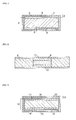
- Fig. 2 shows the structure before being subjected to squeeze casting to form a composite.
- a pair of dense mold release plates 9 coated with mold release agent are positioned vertically opposite each other, and the space in between is filled with diamond powder 10, after which mold members 8 consisting of porous materials capable of being impregnated with aluminum alloy are arranged in contact with the side surface portions so as to sandwich the mold release plates 9 filled with diamond powder 10 from the sides, and in some cases, metal plates 11 are further arranged in contact with the mold release plates 9 from above and below, to form a structure for squeeze casting.
- this structure is filled with a melt of aluminum alloy or the like, the melt passes through the mold members 8 consisting of a porous material and reaches the portion filled with diamond powder 10 to form a composite of diamond powder 10 and aluminum alloy.
- the material of the mold member 8 consisting of a porous material capable of being impregnated with aluminum alloy during squeeze casting is not particularly restricted as long as it is a porous material that can be impregnated with aluminum alloy by squeeze casting.
- the porous material is preferably a porous material of graphite, boron nitride, alumina fiber or the like, having excellent heat resistance and capable of stably supplying melt.
- the dense mold release plates 9 may be stainless steel plates or ceramic plates, and are not particularly limited as long as they are dense materials that are not penetrated by the aluminum alloy during squeeze casting.
- the mold release agent applied to the mold release plates is preferably a mold release agent excelling in heat resistance such as graphite, boron nitride or alumina. Furthermore, by applying the mold release agent after coating the surface of the mold release plates with an alumina sol or the like, it is possible to obtain mold release plates capable of achieving more stable mold release.
- the mold release plates 9 provided on both surfaces are stripped after compositing, and these characteristic features enable an aluminum-diamond composite having a very smooth surface to be obtained.
- metal plate 11 is optional, providing this enables the melt to be evenly impregnated, and allows operations following impregnation such as removal of the aluminum-diamond composite to be easily performed. Additionally, as explained below, a metal plate 11 is provided when a plurality of structures are stacked to form a block.
- the aluminum alloy (metal mainly composed of aluminum) in the aluminum-diamond composite according to the present embodiment should preferably have a low melting point in order to enable sufficient penetration into the cavities in the diamond powder (between diamond particles) during impregnation.
- An example of such an aluminum alloy is, for example, an aluminum alloy comprising 5-25 mass% of silicon. By using an aluminum alloy comprising 5-25 mass% of silicon, it is possible to obtain the effect of promoting the densification of the aluminum-diamond composite.
- magnesium is preferably included in the above aluminum alloy, in order to make the bonding of the diamond particles and ceramic particles with the metal portions stronger.
- metal components in the aluminum alloy other than aluminum silicon and magnesium, there are no particular restrictions as long as it is within a range wherein the properties of the aluminum alloy do not extremely change.
- copper or the like may be included.
- the thickness of the aluminum-diamond composite according to the present embodiment can be adjusted depending on the amount of diamond powder loaded at the time of compositing, and the thickness should preferably be 0.4 to 6 mm.
- the thickness is less than 0.4 mm, there is insufficient strength for use as a heat sink or the like, which is not desirable.
- the thickness exceeds 6 mm, the material itself becomes expensive, and the high thermal conductivity effects of the present invention cannot be adequately achieved, which is not desirable.
- the heating temperature of the blocks is at least 600 °C
- the compositing of the aluminum alloy is stable, and an aluminum-diamond composite having sufficient thermal conductivity can be obtained.
- the heating temperature is 750 °C or less, the formation of aluminum carbides (Al 4 C 3 ) on the diamond powder surface during compositing with the aluminum alloy can be suppressed, resulting in an aluminum-diamond composite having sufficient thermal conductivity.
- the compositing of the aluminum alloy will be stable as long as the pressure at the time of impregnation is at least 20 MPa, resulting in an aluminum-diamond composite having sufficient thermal conductivity. More preferably, the impregnation pressure is at least 50 MPa. As long as the pressure is 50 MPa or more, an aluminum-diamond composite having more stable thermal conductivity properties can be obtained.
- the aluminum-diamond molded article obtained by the above operations may be subjected to an annealing process.
- an annealing process strain can be eliminated from the inside of the above aluminum-diamond molded article, resulting in an aluminum-diamond composite having more stable thermal conductivity properties.
- the anneal should preferably be performed at a temperature of 400 °C to 550 °C for at least 10 minutes.
- the above aluminum-diamond composite is an extremely hard material that is difficult to machine. For this reason, while machining with normal diamond machine tools is possible, waterjet machining, laser machining and electrical discharge machining are preferred for durability of the machine tools and machining cost.
- both surfaces of the composited portion 3 are coated with a covering layer 4 consisting of a material comprising a metal having aluminum as a main component (aluminum alloy).
- the method of formation of the covering layer 4 may be any method.
- the aluminum foil or the like will melt to form a covering layer of aluminum alloy on the surface of the composite.
- the diamond powder 10 may be pre-formed into a molded article, and when loading it between the mold release plates 9, it may be arranged so that an appropriate gap is formed between the mold release plates 9 and the molded article of diamond powder 10, so that the melt will enter into the gap during squeeze casting to form a covering layer 4 consisting of the melt components. Additionally, these methods may be combined.
- the covering layer 4 will mainly consist of a material comprising a metal having aluminum as the main component, substances other than metals having aluminum as the main component may also be included. In other words, the above-mentioned diamond particles or other impurities may also be included.
- diamond particles preferably should not be present at portions 0.01 mm from the surface of the covering layer 4. Due to this arrangement, machining methods that are normally employed in metalworking can be used, resulting in a smooth covering layer without polishing scars.
- the above covering layer preferably comprises at least 80 vol% of a metal having aluminum as a main component.
- the amount of the metal having aluminum as the main component is at least 80 vol%, methods that are normally employed in metalworking can be used, and the covering layer 4 can be polished.
- the amount of the metal having aluminum as the main component it is more preferable for the amount of the metal having aluminum as the main component to be at least 90 vol%. If the amount of the metal having aluminum as the main component is at least 90 vol%, impurities or the like on the inside will not come free and form polishing scars when the surface is being polished.
- the thickness of the covering layer 4 should preferably be at least 0.03 mm and at most 0.2 mm by average thickness. If the average thickness of the covering layer 4 is at least 0.03 mm, the diamond particles will not be exposed by subsequent working, enabling the desired planar precision and plating properties to be easily obtained. Additionally, if the average thickness of the covering layer 4 is 0.2 mm or less, then sufficient thickness can be obtained for the composited portion 3 occupying the resulting aluminum-diamond composite, enabling sufficient thermal conductivity to be achieved.
- the sum of average thicknesses of the covering layers 4 on both surfaces should preferably be 20% or less, more preferably 10% or less, of the thickness of the aluminum-diamond composite 1. If the sum of the average thicknesses of the covering layers 3 on the surfaces of both faces is 20% or less of the thickness of the aluminum-diamond composite 1, then sufficient thermal conductivity can be obtained in addition to planar precision and plating properties.
- the aluminum-diamond composite according to the present embodiment has a structure wherein both faces are coated with a covering layer 4 consisting of a material comprising a metal having aluminum as a main component.
- the surface precision (surface roughness Ra) can be adjusted by working (polishing) this covering layer 4.
- the working of this covering layer 4 may be performed using processing methods that are normally employed in metalworking, for example, by grinding with a buff grinder, to a surface roughness (Ra) of 1 ⁇ m or less.
- the average thickness of the surface layer can be adjusted by working this covering layer 4.
- the surface should preferably be smooth with a low surface roughness, the surface roughness (Ra) being preferably 1 ⁇ m or less, and more preferably 0.5 ⁇ m or less.
- the flatness of the covering layer when converted for a size of 50 mm ⁇ 50 mm, should preferably be 30 ⁇ m or less, and more preferably 10 ⁇ m or less. By having a flatness of 30 ⁇ m or less, the thickness of the bonding layer can be made uniform, enabling a higher heat dissipating ability to be obtained.
- the heat dissipating component for a semiconductor element according to the present embodiment when used as a heat sink for the semiconductor element, will often be used by being attached to the semiconductor element by brazing. Therefore, as shown in Fig. 1 , a surface metal layer 2 will be provided on the bonding surface.
- the method of formation of the surface metal layer 2 may be a method such as plating, vapor deposition, sputtering or the like. When considering the processing costs, plating is preferred, so plating will be explained below.
- the method of plating is not particularly limited, and either electroless plating or electroplating may be used.
- the Ni alloy plating is generally an alloy plating comprising Ni and 5-15 wt% of phosphorus (P), performed by electroless plating.
- P phosphorus
- the resulting Ni alloy plating is amorphous with a film thickness of 0.1 to 2 ⁇ m. If the thickness of the Ni alloy plating is less than 0.1 ⁇ m, there may be pinholes (unplated portions) in the plating film, which is undesirable.
- the peel strength should preferably be at least 5 kgf/cm, and more preferably at least 8 kgf/cm. If the peel strength is less than 5 kgf/cm, when used as a heat dissipating component for a semiconductor element, the temperature load during actual use can result in problems such as separation of the plating layer, which is undesirable.
- the surface of the Ni alloy plating is plated with crystalline Ni with a film thickness of 1 to 5 ⁇ m.
- the plating method is preferably an electroplating method, a electroless plating method may also be used if a crystalline Ni plating film can be obtained. If the thickness of the Ni plating is less than 1 ⁇ m, pinholes (unplated portions) may occur in the plating film, which is undesirable. At more than 5 ⁇ m, the residual stresses occurring in the plating film will increase, and for applications such as the present invention, the temperature load during actual use can cause problems such as separation of the plating film or occurrence of cracks, which is undesirable.
- the ratio between the Ni alloy layer and the Ni layer should preferably be 0.3 or less, and more preferably 0.2 or less. If the ratio between the Ni alloy layer and the Ni layer exceeds 0.3, then in the present application, higher bonding temperatures and increased temperature load during actual use can result in problems such as cracks forming in the surface metal layer.
- the outermost surface is plated with Au by electroplating or electroless plating to a film thickness of 0.05 to 4 ⁇ m. If the plating film thickness is less than 0.05 ⁇ m, the bonding will be insufficient. As for the upper limit, there are no restrictions in terms of the properties, but Au plating is extremely expensive, so it should preferably be 4 ⁇ m or less.
- the aluminum-diamond composite according to the present embodiment should preferably have a thermal conductivity of at least 400 W/mK when the temperature of the aluminum-diamond composite is 25 °C, and a coefficient of thermal expansion of 5 to 10 ⁇ 10 -6 /K from 25 °C to 150 °C.
- the thermal conductivity at 25 °C is at least 400 W/mK and the coefficient of thermal expansion from 25 °C to 150 °C is 5 to 10 ⁇ 10 -6 /K, then a high thermal conductivity and a low rate of thermal expansion of the same level as the semiconductor element can be obtained. Therefore, when used as a heat dissipating component such as a heat sink, it will have excellent heat dissipating properties, and even if the temperature changes, the difference in coefficient of thermal expansion between the semiconductor element and the heat dissipating component is small, so destruction of the semiconductor element can be avoided. As a result, it can be advantageously used as a highly reliable heat dissipating component.
- the heat dissipating component for a semiconductor element using the aluminum-diamond composite of the present invention has a high thermal conductivity and a low coefficient of thermal expansion of the same level as the semiconductor element, so it is suitable for use as a heat dissipating component in an RF element or a semiconductor laser element of GaN, GaAs, SiC or the like requiring high power output.
- it is suitable for use as a heat dissipating component for GaN-HEMT devices or GaAs-HEMT devices which are RF elements.
- the heat dissipating component for a semiconductor element according to Embodiment 2 of the present invention is composed of an aluminum-diamond composite 12 and a surface metal layer 13, as shown in Fig. 3 .
- the aluminum-diamond composite 12 consists of a plate-shaped composited portion 14 consisting of an aluminum-diamond composite material comprising diamond particles and a metal mainly composed of aluminum, and two covering layers 15, 16 provided on both sides of the composited portion 14.
- the diamond particle content is 40 vol% to 70 vol% of the entire aluminum-diamond composite material.
- the covering layer 15 on the composited portion 14 side consists of an aluminum-ceramic composite, while on the other side, the covering layer 16 consists of a metal layer mainly composed of aluminum.
- the surface metal layer 13 consists of an amorphous Ni alloy layer 17, a Ni layer 18 and an Au layer 19.
- the heat dissipating component for a semiconductor element of this structure also has high thermal conductivity and a coefficient of thermal expansion close to that of the semiconductor element, and furthermore, provides the effect of being able to suppress the occurrence of cracks or the like at the surface metal layer portion even upon actual use under high duress.
- the heat dissipating component for a semiconductor element according to Embodiment 2 differs from the structure in Embodiment 1 in that the covering layer of the aluminum-diamond composite 12 is composed of a covering layer 15 consisting of an aluminum-ceramic composite on the composited portion 14 side and a covering layer 16 consisting of a metal layer mainly composed of aluminum on the other side.
- the embodiment will be explained in detail together with the method of production, focusing on the portions that are different in structure, but those portions that are not explained are the same as Embodiment 1.
- a portion comprising a plate-shaped composited portion 14 consisting of an aluminum-diamond composite material and a covering layer 15 consisting of an aluminum-ceramic composite coated onto the composited portion 14 is first produced.
- a plate-shaped composited portion 14 consisting of an aluminum-diamond composite material
- a covering layer 15 consisting of an aluminum-ceramic composite coated onto the composited portion 14 is first produced.
- a mold member 10 consisting of a porous material capable of being impregnated with an aluminum alloy, a ceramic porous body 21, a dense mold release plate 22 coated with a mold release agent and a diamond powder 23 are arranged to form a structure for squeeze casting, and after compositing an aluminum alloy by squeeze casting, the aluminum-ceramic composite present on the outer surface portions of the aluminum-diamond composite after compositing are ground to produce a structure wherein both surfaces of a composited portion 14 are coated with a covering layer 15 consisting of an aluminum-ceramic composite of thickness 0.05 to 0.2 mm.
- this structure is machined by a waterjet cutter or a laser cutter, after which a covering layer 16 of thickness 0.05 to 2.0 ⁇ m is formed on the surface thereof.
- the ceramic porous body 21 is a porous body of a porous material capable of being impregnated by an aluminum alloy by squeeze casting, comprising at least one of silicon carbide, silicon nitride and aluminum nitride, among which silicon carbide is preferable for the thermal conductivity of the resulting aluminum-ceramic composite.
- the porosity of the ceramic porous body should be such that there are sufficient pores to enable impregnation of aluminum alloy by squeeze casting, which is 20 to 60 vol%.
- the ceramic content in the aluminum-ceramic composite should preferably be adjusted to make the difference in coefficient of thermal expansion between the aluminum-diamond composite and the aluminum-ceramic composite as small as possible. When the difference in coefficient of thermal expansion between the aluminum-diamond composite and the aluminum-ceramic composite is large, warping may occur during subsequent processing steps, which is not desirable.
- an aluminum-ceramic composite present on the outer surface portion of the aluminum-diamond composite is ground to produce a structure wherein both surfaces of a composited portion 14 are coated with a covering layer 15 consisting of an aluminum-ceramic composite of thickness 0.05 to 0.2 mm.
- the grinding is performed using diamond machine tools and diamond abrasive grains.
- a waterjet cutter, laser cutter or electrical discharge cutter should be used.
- both surfaces of the composited portion 14 are coated with a covering layer 15 consisting of an aluminum-ceramic composite of thickness 0.05 to 0.2 mm, and as mentioned above, this covering layer 15 is formed together with the composited portion 14 by squeeze casting, but as a different method, it is possible to prepare only the aluminum-ceramic composite beforehand, then join the aluminum-diamond composite to the composited portion 14 during the production process, to produce the aluminum-diamond composite 12 of Fig. 3 .
- the thickness of the above-mentioned covering layer 15 consisting of an aluminum-ceramic composite should preferably be at least 0.05 mm and at most 0.2 mm. If the thickness of the covering layer 15 is at least 0.05 mm, then it is easy to obtain the desired planar precision (surface roughness). Additionally, if the average thickness of the covering layer 15 is at most 0.2 mm, then although also dependent on the thickness of the resulting aluminum-diamond composite 12, it is possible to obtain sufficient thickness for the composited portion 14 occupying the composite 12 and to ensure sufficient thermal conductivity.
- the aluminum-diamond composite 12 has a structure wherein both surfaces are coated with a covering layer 15 consisting of an aluminum-ceramic composite, so the surface precision (surface roughness Ra) and flatness can be adjusted by machining (polishing) the covering layer 15.
- This machining can be performed by employinging methods using diamond abrasive grains or diamond grindstones, for example, by grinding with a grinding plate or the like, then polishing with a buff polisher to a surface roughness (Ra) of 1 ⁇ m or less.
- Ra surface roughness
- the average thickness of the surface layer can also be adjusted by working this covering layer 15.
- the plating adhesion is improved by cleaning the surface of the aluminum-diamond composite 12 on which the covering layer 15 is formed, and forming a further covering layer 16 consisting of a metal mainly composed of aluminum with a thickness of 0.05 to 2.0 ⁇ m on the surface. If the thickness of this covering layer 16 is less than 0.05 ⁇ m, then there may be portions not covered by the covering layer, or the covering layer may react during the plating pretreatment, forming pinholes which can result in unplated portions, thereby reducing the chemical resistance.
- the covering layer thickness exceeds 2.0 ⁇ m, the difference in coefficient of linear thermal expansion between the covering layer 16 and the composite can result in differences in thermal expansion of the materials which may lead to generation of stress or separation.
- the thickness of the covering layer 16 should more preferably be 0.3 to 0.6 ⁇ m.
- the covering layer 16 is formed by vapor deposition or sputtering to a thickness of 0.05 to 2.0 ⁇ m.
- the aluminum alloy constituting the covering layer 16 is either pure aluminum or an aluminum alloy comprising at least 70 mass% aluminum. If the aluminum content is less than 70 mass%, then it is not possible to provide Ni plating with sufficient adhesion by a zincate treatment.
- the metal components in the aluminum alloy aside from aluminum and silicon as long as it is within a range wherein the properties do not greatly change. For example, magnesium, copper or the like may be included.
- the adhesion between the covering layer 16 of aluminum alloy or the like and the covering layer 15 consisting of an aluminum-ceramic composite on the surface of the aluminum-diamond composite 12 should preferably be improved by subjecting to a heat treatment for at least 1 minute at a temperature of 460 to 650 °C in an atmosphere of nitrogen, argon, hydrogen, helium or a vacuum. If the treatment is performed in an oxidative atmosphere, an oxide film can be formed on the surface, which can lead to subsequent plating defects.
- the temperature is preferably 480 to 570 °C. If the temperature is 460 °C or less, then the adhesion between the covering layer 15 and the covering layer 16 becomes poor, and if the temperature is 650 °C or more, then the metal covering layer 16 can melt and cause the surface roughness to deteriorate.
- the heat dissipating component for a semiconductor element according to Embodiment 3 is composed of an aluminum-diamond composite 24 and a surface metal layer 25.
- the aluminum-diamond composite 24 consists of a plate-shaped composited portion 26 consisting of an aluminum-diamond composite material and covering layers 27 provided on both surfaces of the composited portion 26.
- the covering layer 27 consists of an aluminum-ceramic fiber composite material
- the surface metal layer 25 consists of an amorphous Ni alloy layer 28, a Ni layer 29 and an Au layer 30.
- the heat dissipating component according to the present Embodiment 3, as shown in Fig. 6 involves compositing the aluminum alloy by squeeze casting with ceramic fibers 32 arranged between the dense mold release plates 33 to which a mold release agent has been applied and the diamond powder 34 loaded between the mold release plates 33, to obtain an aluminum-diamond composite 24 on which a covering layer 27 consisting of an aluminum-ceramic fiber composite has been formed on both surfaces of a composited portion 26.
- the above-mentioned covering layer 27 consisting of an aluminum-ceramic fiber composite should have a content of less than 20 vol% of components other than aluminum alloy in accordance with the relationship between platability and surface precision. If the content of components other than aluminum alloy is less than 20 vol%, the covering layer 27 can be easily processed.
- ceramic fiber is not particularly limited, ceramic fibers such as alumina fibers, silica fibers, mullite fibers and graphite fibers are preferably used for their heat resistance. Additionally, the ceramic fiber content (Vf) should preferably be 10 vol% or less in view of the properties of the aluminum-ceramic fiber composite, and Vf should preferably be less than 20 vol% when stacked and compressed.
- the thickness of the ceramic fibers should preferably be 0.5 mm or less. If 0.5 mm or less, then the thickness of the surface layer can be appropriately set, and an aluminum-diamond composite having sufficient thermal conductivity can be obtained.
- Embodiment 3 is the same as Embodiment 1.
- the heat dissipating component for a semiconductor element has covering layers (4; 15, 16; 27) formed on both faces of a plate-shaped composited portion (3; 14; 26) consisting of an aluminum-diamond composite material to form an aluminum-diamond composite (1; 12; 24), with surface metal layers (2; 13, 25) provided on both main faces of the aluminum-diamond composite (1; 12; 24) by forming an amorphous Ni alloy layer (5; 17; 28), Ni layer (6; 18; 29) and Au layer (7; 19; 30) in order from the main faces.
- the covering layers consist of a metal layer mainly composed of aluminum (covering layer 4; Embodiment 1), an aluminum-ceramic composite layer (covering layer 15) and a metal layer (covering layer 16) (Embodiment 2), or an aluminum-ceramic fiber composite layer (covering layer 27; Embodiment 3).
- the aluminum-diamond composite has a high thermal conductivity and a coefficient of thermal expansion close to that of the semiconductor element. Furthermore, the surface metal layer improves the platability of the surface, and the surface has low surface roughness and flatness, making it appropriate for use as a heat dissipating component such as a heat sink for dissipating heat from semiconductor elements.
- the thickness of the covering layer 4 is 0.03 to 0.2 mm
- the thickness of the covering layer 15 is 0.05 to 0.2 mm
- the thickness of the covering layer 27 is 0.05 to 0.2 mm
- the thickness of the bonding layer can be made uniform, enabling a higher heat dissipating ability to be obtained.
- the thickness of the above plate-shaped aluminum-diamond composite (1; 12; 24) is 0.4 to 6 mm, it has sufficient strength and heat dissipating properties for use as a heat dissipating component such as a heat sink.
- the aluminum-diamond composite may have a thermal conductivity of at least 400 W/mK when the temperature is 25 °C, and the aluminum-diamond composite may have a coefficient of thermal expansion of 5 to 10 ⁇ 10 -6 /K from 25 °C to 150 °C.
- a heat dissipating component such as a heat sink
- it will excel in heat dissipating properties, and destruction of the semiconductor element can be avoided even if subjected to temperature changes, because the difference in coefficient of thermal expansion between the semiconductor element and the heat dissipating component is small.
- At least both main faces of the aluminum-diamond composite (1; 12; 24) are provided with a surface metal layer (2; 13; 25) obtained by forming an amorphous Ni alloy layer (5; 17; 28), Ni layer (6; 18; 29) and Au layer (7; 19; 30) in order from the main faces, and the ratio between the Ni alloy layer and the Ni layer (Ni alloy layer thickness/Ni layer thickness) is set to be 0.3 or less, enabling bonding by brazing or the like.
- a heat dissipating component or the like to be bonded with a high-power semiconductor element it is possible to achieve high reliability enabling cracking or the like of the surface metal layer portions to be suppressed even during actual use with a heavy load.
- the heat dissipating component for a semiconductor element having the above structure when used as a heat dissipating component or the like by bonding to a high-power semiconductor element, has high heat dissipating properties, and is capable of achieving high reliability enabling cracking or the like of the surface layer metal portions to be suppressed even during actual use with a heavy load, so it is suitable for use as a heat dissipating component for RF elements or semiconductor lasers of GaN, GaAs, SiC or the like.
- high-purity diamond powder A (average grain size 180 ⁇ m), high-purity diamond powder B (average grain size 20 ⁇ m), high-purity diamond powder C (average grain size 2 ⁇ m) and aluminum powder (average grain size 30 ⁇ m) were mixed at the blending ratios shown in Table 1.
- a 40 ⁇ 40 ⁇ 2 mmt stainless steel plate (SUS430 material) was coated with an alumina sol and baked for 30 minutes at 350 °C, then a graphite mold release agent was applied to the surface to produce a mold release plate (mold release plate 9 of Fig. 2 ).
- the diamond powders of Table 1 were loaded into an isotropic graphite jig (mold member 8 of Fig. 2 ) of 20% porosity having a 60 ⁇ 60 ⁇ 8 mmt outer shape and a 40 ⁇ 40 ⁇ 8 mmt hole in a central portion, with pure aluminum foil of thickness 30 ⁇ m disposed above and below, and both faces were sandwiched by mold release plate 9 to form a structure.
- a plurality of the above structures were stacked with 60 ⁇ 60 ⁇ 1 mmt stainless steel plates coated with graphite mold release agent (metal plate 11 of Fig. 2 ) in between, iron plates of thickness 12 mm were placed on both sides, and these were attached with six M10 bolts and tightened with a torque wrench to a planar clamping torque of 10 Nm to form a single block.
- the resulting block was preheated in an electrical furnace to a temperature of 650 °C, then placed in a preheated press mold of inner diameter 300 mm, into which an aluminum alloy melt at temperature 800 °C comprising 12 mass% silicon and 1 mass% magnesium was poured, and compressed for 20 minutes at a pressure of 100 MPa to impregnate the diamond powder with the aluminum alloy.
- the block was cut along the shape of the mold release plates using a wet-type bandsaw, and the sandwiched stainless steel plates were stripped. Then, an anneal was performed for 3 hours at 530 °C to remove the strain of impregnation to obtain an aluminum-diamond composite.
- the resulting aluminum-diamond composite was polished on both surfaces using #600 polishing paper, then buffed.
- a waterjet cutter (Sugino Machine Abrasive Jet Cutter NC) was used with garnet of grain size 100 ⁇ m as the polishing abrasive grains at conditions of pressure 250 MPa and processing speed 50 mm/min to work the block to a shape of 25 ⁇ 25 ⁇ 2 mmt to obtain an aluminum-diamond composite.
- a cross section of the resulting aluminum-diamond composite was observed by factory microscope to measure the average thickness of the covering layer on both surfaces (covering layer 4 of Fig. 1 ). Additionally, the surface roughness (Ra) was measured with a surface roughness meter and the flatness was measured by three-dimensional profile measurement. The results are shown in Table 2.
- a sample for measurement of coefficient of thermal expansion (3 ⁇ 2 ⁇ 10 mm) and a sample for measurement of thermal conductivity (25 ⁇ 25 ⁇ 2 mmt) were produced by waterjet machining.
- the respective sample pieces were used to measure the coefficient of thermal expansion from temperatures of 25 °C to 150 °C using a thermal expansion meter (Seico Electronics TMA300) and the thermal conductivity at 25 °C by laser flash analysis (Rigaku LF/TCM-8510B). The results are shown in Table 2.
- Example 1 The density of the aluminum-diamond composite of Example 1 was found by Archimedes' principle to be 3.21 g/cm 3 . Furthermore, bending strength test samples (3 ⁇ 2 ⁇ 40 mm) were produced for Example 1, and the 3-point bending strength as measured by a bending strength tester was found to be 320 MPa.
- Table 2 Type Average Thickness of Covering Layer (mm) Surface Roughness Ra ( ⁇ m) Flatness ( ⁇ m) Thermal Conductivity (W/mK) Coefficient of Thermal Expansion ( ⁇ 10 -6 /K)
- Example 1 0.05 0.20 8 570 7.0
- Example 2 0.05 0.25 5 530 8.0
- Example 3 0.05 0.23 12 450 9.0
- Example 4 0.05 0.19 6 600 5.5
- electroless Ni-P, electro Ni and electro Au plating were performed to form plating layers (metal surface layers 2 of Fig. 1 ) of thickness 5 ⁇ m (Ni-P: 0.3 ⁇ m + Ni: 2.7 ⁇ m + Au: 2.0 ⁇ m) on the surfaces of the aluminum-diamond composites of Examples 1-4.
- plating layers metal surface layers 2 of Fig. 1
- Ni-P 0.3 ⁇ m + Ni: 2.7 ⁇ m + Au: 2.0 ⁇ m
- the aluminum-diamond composites of Examples 1-4 were extremely smooth with a surface roughness of 0.19 to 0.25 ⁇ m, and had high thermal conductivity and a coefficient of thermal expansion close to semiconductor elements.
- a diamond powder A (average particle size 190 ⁇ m)
- 15 g of a diamond powder B (average particle size 20 ⁇ m)
- 16 g of a silica powder (average particle size 5 ⁇ m)
- 16 g of a silicon powder (average particle size 10 ⁇ m)
- An aluminum-diamond composite was produced in the same manner as Example 1, except that a diamond powder having a layer of ⁇ -type silicon carbide formed on the surface was used as the diamond powder.
- the resulting aluminum-diamond composites were subjected to the same polishing and machining as Example 1 and worked to a shape of 25 ⁇ 25 ⁇ 2 mmt to form aluminum-diamond composites, and cross sections of the aluminum-diamond composites were observed with a factory microscope to measure the average thickness of the covering layer (covering layer 4 in Fig. 1 ) on both surfaces, as a result of which the average thickness of the covering layer was found to be 0.05 mm. Additionally, the surface roughness (Ra) as measured with a surface roughness meter was 0.21 ⁇ m, and the flatness as measured by a three-dimensional shape measuring device was 7 ⁇ m.
- Example 5 the aluminum-diamond molded article of Example 5 was subjected to the same property evaluations as Example 1, upon which the density was found to be 3.20 g/cm 3 , the coefficient of thermal expansion from temperatures of 25 °C to 150 °C was 7.2 ⁇ 10 -6 /K, the thermal conductivity at a temperature of 25 °C was 650 W/mK and the three-point bending strength was 340 MPa.
- a plating layer (metal surface layer 2 of Fig. 1 ) of thickness 5 ⁇ m (Ni-P: 0.3 ⁇ m + Ni: 2.7 ⁇ m + Au: 2.0 ⁇ m) was formed on the surfaces of the aluminum-diamond composite as with Example 1. Upon measuring the peel strength of the resulting plated product, it was found to be 12 kgf/cm.
- Example 5 a diamond powder having a layer of ⁇ -type silicon carbide formed on the surface was used. As a result, a high thermal conductivity of 650 W/mK and a coefficient of thermal expansion close to that of a semiconductor element were obtained.
- Example 1 Aluminum-diamond composites were prepared in the same way as in Example 1 except that the loaded amount of diamond powder was changed from that of Example 1, to form structures with a plate thickness of 0.4 mm in Example 6 and 6.0 mm in Example 7, and with a pure aluminum foil with a thickness of 15 ⁇ m in Example 8 and a thickness of 200 ⁇ m in Example 9 above and below the diamond powder at the time of stacking.
- the resulting aluminum-diamond composites were subjected to the same polishing and machining as Example 1 and worked to a shape of 25 ⁇ 25 ⁇ 2 mmt to form aluminum-diamond composites, cross sections of the aluminum-diamond composites were observed with a factory microscope to measure the average thickness of the covering layer (covering layer 4 in Fig. 1 ) on both surfaces, the surface roughness (Ra) was measured with a surface roughness meter, and the flatness was measured by a three-dimensional shape measuring device, the results being shown in Table 3.
- Example 3 Type Average Thickness of Covering Layer (mm) Surface Roughness Ra ( ⁇ m) Flatness ( ⁇ m) Thermal Conductivity (W/mK) Coefficient of Thermal Expansion ( ⁇ 10 -6 /K)
- Example 6 0.05 0.25 15 480 7.5
- Example 7 0.05 0.20 4 600 6.8
- Example 8 0.03 0.21 7 580 6.8
- Example 9 0.20 0.35 16 530 8.0
- a plating layer (metal surface layer 2 of Fig. 1 ) of thickness 5 ⁇ m (Ni-P: 0.3 ⁇ m + Ni: 2.7 ⁇ m + Au: 2.0 ⁇ m) was formed on the surfaces of the aluminum-diamond composites as with Example 1.
- the resulting plated products were measured as to peel strength, and the plating film was observed after a 1000-cycle heat cycle test of holding for 30 minutes at a temperature of -55 °C at atmospheric pressure and holding for 30 minutes at a temperature of 175 °C.
- the results are shown in Table 4.
- Table 4 Type Peel Strength (kgf/cm) Surface State after Heat Cycle Test
- Example 6 12 No peeling or cracking
- Example 7 13
- Example 8 11
- Example 9 No peeling or cracking
- An aluminum-diamond composite produced according to Example 1 was ultrasonically cleaned before plating, after which plating layers (surface metal layers 2 of Fig. 1 ) were formed on the surfaces of the aluminum-diamond composite under the conditions shown in Table 5.
- the resulting plated products were measured as to their peel strength, and subjected to a 1000-cycle heat cycle test of holding for 30 minutes at a temperature of -55 °C at atmospheric pressure and holding for 30 minutes at a temperature of 175 °C, after which the plating films were observed. The results are shown in Table 6.
- the diamond powder was loaded into an isotropic graphite jig (mold member 20 of Fig. 4 ) with a porosity of 20% having external dimensions of 60 ⁇ 60 ⁇ 8 mmt and a hole of 40 ⁇ 40 ⁇ 8 mmt in a central portion, so as to be sandwiched from both sides with a 40 ⁇ 40 ⁇ 3.1 mmt silicon carbide porous body (ceramic porous body 21 of Fig. 4 ) with a porosity of 35% to form a structure.
- an isotropic graphite jig (mold member 20 of Fig. 4 ) with a porosity of 20% having external dimensions of 60 ⁇ 60 ⁇ 8 mmt and a hole of 40 ⁇ 40 ⁇ 8 mmt in a central portion, so as to be sandwiched from both sides with a 40 ⁇ 40 ⁇ 3.1 mmt silicon carbide porous body (ceramic porous body 21 of Fig. 4 ) with a porosity of 35%
- a plurality of the above structures were stacked with 60 ⁇ 60 ⁇ 1 mmt mold release plates coated with graphite mold release agent (mold release plate 22 of Fig. 4 ) in between, iron plates of thickness 12 mm were placed on both sides, and these were attached with six M10 bolts and tightened with a torque wrench to a planar clamping torque of 10 Nm to form a single block.
- the resulting block was preheated in an electric furnace to a temperature of 650 °C, then placed in a preheated press mold of inner dimensions 300 mm, an aluminum alloy melt of temperature 800 °C comprising 12 mass% silicon and 1 mass% magnesium was poured in, and compressed for 20 minutes at a pressure of 100 MPa to impregnate the diamond powder with aluminum alloy.
- the blocks were cut along the shapes of the mold release plates using a wet bandsaw, and the mold release plates were stripped. Then, annealing was performed for three hours at 530 °C in order to remove the strain from impregnation to obtain an aluminum-diamond composite.
- the resulting aluminum-diamond composites were polished on both surfaces to the plate thicknesses of Table 5 with a planar polishing plate using #230 diamond abrasive grains, then buffed. In Example 19, both surfaces were polished with #230 diamond abrasive grains, but were not buffed.
- Example 16 1.9 0.05 0.15 2 570 6.9
- Example 17 2.0 0.10 0.14 1 550 7.0
- Example 18 2.2 0.20 0.16 2 500 7.1
- Example 19 2.0 0.10 0.95 2 550 7.0 Comparative Example 4 2.0 0.10 0.15 2 550 7.0
- an aluminum layer (covering layer 16 of Fig. 3 ) of thickness 0.5 ⁇ m was formed on the surface of the composite by vapor deposition, and a heat treatment was performed for 30 minutes at a temperature of 500 °C in a nitrogen atmosphere.
- the above aluminum layer was not formed in Comparative Example 4.
- a plating layer (surface metal layer 14 of Fig 3 ) was formed in the same manner as Example 1 on the aluminum-diamond composite having an aluminum layer formed on the surface.
- the aluminum-diamond composites according to Examples 16-19 had a high thermal conductivity and a coefficient of thermal expansion close to that of semiconductor elements, and by forming an appropriate surface metal layer on the composite surface, ensured adequate plating adhesion, and was able to suppress the generation of cracks in the surface metal layer portions even after heat cycle tests simulating actual use under high duress.
- Example 9 Type Type of Ceramic Fiber Ceramic Fiber Content Vf (vol%) Ceramic Fiber Thickness (mm)
- Example 20 alumina 5 0.1
- Example 21 alumina 10 0.1
- Example 22 alumina 20 0.1
- Example 23 alumina 10 0.05
- Example 24 mullite 10 0.2
- Example 25 graphite 10 0.1
- a plurality of the above structures were stacked with 60 ⁇ 60 ⁇ 1 mmt mold release plates coated with graphite mold release agent (mold release plate 33 of Fig. 6 ) in between, iron plates of thickness 12 mm were placed on both sides, and these were attached with six M10 bolts and tightened with a torque wrench to a planar clamping torque of 10 Nm to form a single block.
- the resulting block was preheated in an electric furnace to a temperature of 700 °C, then placed in a preheated press mold of inner dimensions 300 mm, an aluminum alloy melt of temperature 850 °C comprising 1 mass% magnesium was poured in, and compressed for 20 minutes at a pressure of 100 MPa to impregnate the diamond powder with aluminum alloy.
- the blocks were cut along the shapes of the mold release plates using a wet bandsaw, and the mold release plates were stripped. Then, annealing was performed for three hours at 530 °C in order to remove the strain from impregnation to obtain an aluminum-diamond composite.
- the resulting aluminum-diamond composites were machined to dimensions of 25 ⁇ 25 ⁇ 2 mmt by performing the same polishing and working as Example 1, to form aluminum-diamond composites, and cross-sections of the aluminum-diamond composites were observed through a factory microscope to measure the average thickness of the covering layers on both sides (covering layer 27 consisting of an aluminum-ceramic fiber composite layer in Fig. 5 ), the surface roughness (Ra) measured with a surface roughness meter, and the flatness measured by a three-dimensional profile measuring device. The results are shown in Table 10.
- Example 10 Type Plate Thick. (mm) Covering Layer Thick. (mm) Surface Rough. Ra ( ⁇ m) Flatness ( ⁇ m) Thermal Cond. (W/mK) Coeff. Thermal Expansion (x 10 -6 /K)
- Example 20 2.0 0.10 0.28 12 560 7.2
- Example 21 2.0 0.10 0.31 11 550 7.1
- Example 22 2.0 0.10 0.30 12 550 7.1
- Example 23 1.9 0.05 0.33 9 570 7.0
- Example 24 2.2 0.20 0.27 18 530 7.5
- Example 25 2.0 0.10 0.36 15 570 7.0
- a plating layer (metal surface layer 25 of Fig. 5 ) of thickness 5 ⁇ m (Ni-P: 0.3 ⁇ m + Ni: 2.7 ⁇ m + Au: 2.0 ⁇ m) was formed on the surfaces of the aluminum-diamond composite as with Example 1.
- the resulting plated products were measured as to their peel strength, and subjected to a 1000-cycle heat cycle test of holding for 30 minutes at a temperature of -55 °C at atmospheric pressure and holding for 30 minutes at a temperature of 175 °C, after which the plating films were observed. The results are shown in Table 11.
- the aluminum-diamond composites according to Examples 20-25 had a high thermal conductivity and a coefficient of thermal expansion close to that of semiconductor elements, and by forming an appropriate surface metal layer on the composite surface, ensured adequate plating adhesion, and was able to suppress the generation of cracks in the surface metal layer portions even after heat cycle tests simulating actual use under high duress.
Abstract
Description
- The present invention relates to a heat dissipating component for a semiconductor element.
- In general, with semiconductor elements that are used for optical communications such as semiconductor laser elements and RF elements, the issue of how to efficiently dissipate heat generated from the elements is very important for preventing operation failures. In recent years, progress in the art of semiconductor elements has been accompanied by higher power, higher speed and higher integration of elements, placing stricter demands on the ability to dissipate heat. For this reason, high thermal conductivity is generally required in heat dissipating components such as heat sinks, so copper (Cu) which has a high thermal conductivity of 390 W/mK is used.
- On the other hand, individual semiconductor elements have become larger in size with higher power, and the problem of mismatches between the thermal expansion of semiconductor elements and the heat sinks used for heat dissipation has become more apparent. In order to solve these problems, the development of a heat sink material having both the property of high thermal conductivity and a coefficient of thermal expansion matching that of semiconductor elements has been sought. As such materials, composites of metals and ceramics, such as composites of aluminum (Al) and silicon carbide (SiC), have been proposed (Patent Document 1).
- However, no matter how the conditions are optimized in an Al-SiC composite, the thermal conductivity is 300 W/mK or less, so the development of a heat sink material having a thermal conductivity that is even higher than the thermal conductivity of copper has been sought. As such a material, a metal-diamond composite combining the high thermal conductivity of diamond and the high coefficient of thermal expansion of metals, having a high thermal conductivity and a coefficient of thermal expansion close to that of semiconductor element materials has been proposed (Patent Document 2).
- Additionally,
Patent Document 3 describes forming a β-type SiC layer on the surface of diamond particles to suppress the generation of metal carbides of low thermal conductivity formed during compositing and to improve the wettability with molten metals, thereby improving the thermal conductivity of metal-diamond composites. - Furthermore, since diamond is a very hard material, the metal-diamond composites obtained by compositing with metals are similarly very hard, and therefore difficult to work. For this reason, metal-diamond composites are almost unworkable with normal diamond tools, so in order to use metal-diamond composites as heat sinks which are compact and exist in various shapes, there is the issue of how to shape them at low cost. In response to this issue, laser machining and waterjet machining have been considered, and since metal-ceramic composites can pass electricity, methods of machining by electrical discharge have also been considered.
- With heat dissipating components for use with semiconductor elements, a metal layer must be added to the surface of the heat dissipating component by coating or the like in order to enable them to be attached to the elements. In the case of normal semiconductor elements, bonding by solder is most common, with a bonding temperature of 300 °C or less, so a metal layer is provided on the surface by plating a Ni-P alloy or the like. However, regarding the manner of use of materials for heat sinks, heat sinks are usually arranged in contact with the semiconductor element by bonding with a brazing material in order to enable efficient dissipation of the heat generated by the semiconductor element. For this reason, multilayered plating having metal plating added to the bonding surface is used. Furthermore, with this manner of use, higher bonding temperatures and increases in the temperature load at the time of actual use can cause amorphous metals to crystallize in conventional alloy plating such as Ni-P alloys, and the change in volume can result in formation of microcracks, with the cracks being extended with subsequent temperature loads.
- Furthermore, when a heat sink is bonded to a semiconductor element with brazing materials or the like, the planar precision of the bonding boundary is important for heat dissipation. In the case of conventional metal-diamond composites, diamond particles are exposed on the contact surface, making the contact surface rough, and consequently increasing the thermal resistance of the contact boundary, which is undesirable. For this reason, there is also the issue of how to reduce the roughness of the surface as a property sought in heat sink materials.
Patent Document 1: JP H9-157773 A Patent Document 2: JP 2000-303126 A Patent Document 3: JP 2007-518875 A - The present invention was made in view of the above-described circumstances, and has the purpose of offering a heat dissipating component for a semiconductor element having both a high thermal conductivity and a coefficient of thermal expansion close to that of semiconductor elements, that has improved surface roughness flatness of the surface so as to be suitable for use as a heat sink for a semiconductor element, and does not crack at surface metal layer portions even upon actual use under high duress.
- In other words, the present invention offers a heat dissipating component for a semiconductor element, comprising an aluminum-diamond composite formed by covering both main faces of a plate-shaped body of thickness 0.4 to 6 mm comprising 40 vol% to 70 vol% diamond particles, the balance consisting of a metal having aluminum as a main component, with a covering layer consisting of a metal having aluminum as a main component or an aluminum-ceramic composite material; wherein (1) an amorphous Ni alloy layer of film thickness 0.1 to 1 µm, (2) a Ni layer of
film thickness 1 to 5 µm, and (3) an Au layer of film thickness 0.05 to 4 µm are formed, sequentially from a main face side, on both main faces of the aluminum-diamond composite, such that a ratio between the Ni alloy layer and the Ni layer (Ni alloy layer thickness/Ni layer thickness) is 0.3 or less. - In one embodiment, the covering layer is a metal layer of film thickness 0.03 to 0.2 mm comprising at least 80 vol% of a metal having aluminum as a main component, and in another embodiment, the covering layer is a layer comprising, from a plate-shaped body side, an aluminum-ceramic composite layer of film thickness 0.05 to 0.2 mm, and a metal layer of film thickness 0.1 to 2 µm, having aluminum as a main component. Additionally, in yet another embodiment, the covering layer is aluminum-ceramic fiber composite layer of film thickness 0.05 to 0.2 mm comprising at least 80 vol% of a metal having aluminum as a main component.
- In another embodiment, the Ni alloy layer, Ni layer and Au layer are formed by plating, the underlying Ni alloy layer is formed by electroless plating pre-treated by zinc substitution, and the peel strength of the plating film is at least 5 kg/cm, and in yet another embodiment, the semiconductor element is an RF element or semiconductor laser element consisting of GaN, GaAs or SiC.
- Furthermore, in another embodiment of the present invention, the aluminum-diamond composite is produced by squeeze casting, and/or has a thermal conductivity at 25 °C of at least 400 W/mK and a coefficient of thermal expansion from 25 °C to 150 °C of 5 × 10⁻⁶ to 10 × 10-6/K.
- Additionally, in another embodiment of the present invention, the aluminum-diamond composite in the heat dissipating component of the present invention is an aluminum-diamond composite in which the diamond particles are characterized by the presence of a layer of β-type silicon carbide chemically bonded to a surface thereof.
- In the heat dissipating component for a semiconductor element consisting of the above arrangement, the aluminum-diamond composite has a high thermal conductivity and a coefficient of thermal expansion close to that of the semiconductor element, and the surface metal layer is provided with a specific layer structure, so it is capable of suppressing the occurrence of cracks and the like in the surface metal layer portions even upon actual use under high duress.
-
- [
Fig. 1 ] A schematic section view showing the structure of a heat dissipating component for a semiconductor element according toEmbodiment 1 of the present invention. - [
Fig. 2 ] A schematic section view for explaining one step in producing a composited portion of an aluminum-ceramic composite constituting the heat dissipating component for a semiconductor element ofFig. 1 . - [
Fig. 3 ] A schematic section view showing the structure of a heat dissipating component for a semiconductor element according toEmbodiment 2 of the present invention. - [
Fig. 4 ] A schematic section view for explaining one step in producing a composited portion of an aluminum-ceramic composite constituting the heat dissipating component for a semiconductor element ofFig. 3 . - [
Fig. 5 ] A schematic section view showing the structure of a heat dissipating component for a semiconductor element according toEmbodiment 3 of the present invention. - [
Fig. 6 ] A schematic section view for explaining one step in producing a composited portion of an aluminum-ceramic composite constituting the heat dissipating component for a semiconductor element ofFig. 5 . - The terminology and symbols used in the present specification and claims have the meaning that is normally understood by those skilled in the art. In particular, in the present specification, the word "to" refers to a range that is inclusive from "at least" to "at most". Therefore, for example, "A to B" refers to a range of at least A and at most B.
- Additionally, in the present specification, "both faces" and "both main faces" of a plate-shaped body refer to the two opposing faces of the plate-shaped body, while "side face portion" refers to the faces roughly perpendicular to both faces. Therefore, "both faces" and "both main faces" of an aluminum-diamond composite formed in the shape of a plate refer to the upper and lower faces of the composite, and "side face portion" refers to the portions roughly perpendicular to both faces.
- Herebelow, an embodiment of the heat dissipating component for a semiconductor element according to the present invention will be explained with reference to the attached drawings.
- As shown in
Fig. 1 , the heat dissipating component for a semiconductor element according toEmbodiment 1 of the present invention is composed of an aluminum-diamond composite 1 and asurface metal layer 2. The aluminum-diamond composite 1 consists of a plate-shaped composite portion 3 consisting of an aluminum-diamond composite material comprising diamond particles and a metal having aluminum as a main component, and acovering layer 4 provided on both faces of thecomposite portion 3. In the aluminum-diamond composite material, the diamond particle content is 40 vol% to 70 vol% of the aluminum-diamond composite material overall. Thecovering layer 4 consists of a material comprising a metal containing aluminum, and thesurface metal layer 2 consists of an amorphousNi alloy layer 5,Ni layer 6 andAu layer 7. - The heat dissipating component for a semiconductor element of this structure has high thermal conductivity and a coefficient of thermal expansion close to that of semiconductor elements, and further has the effect of suppressing the occurrence of cracks or the like on the surface metal layer portion even upon actual use under high duress.
- Herebelow, the structure of a heat dissipating component for a semiconductor element according to
Embodiment 1 will be described together with its production method. - In general, methods for producing aluminum-diamond composites can be divided largely into two types, these being impregnation and powder metallurgy. Of these, those that are actually on the market are mostly formed by impregnation for their properties such as thermal conductivity. There are various methods of impregnation, including those performed at standard pressure, and high-pressure forging performed at high pressure. High-pressure forging includes squeeze casting and die casting. A suitable method for the present invention is high-pressure forging wherein impregnation is performed at a high pressure, and squeeze casting is preferred in order to obtain dense composites excelling in properties such as thermal conductivity. Squeeze casting generally refers to a method involving filling a high-pressure vessel with a powder such as diamond or a compact, and impregnating this with molten aluminum alloy or the like at high temperature and high pressure to obtain a composite material.
- The diamond powder used as the raw material may be a natural diamond powder or an artificial diamond powder. Additionally, a binder such as silica may be added to the diamond powder as needed, and a compact can be formed by adding a binder.
- Regarding the granularity of the diamond powder, a powder with an average grain size of at least 50 µm is preferable, and an average grain size of at least 100 µm is even more preferable for the purposes of achieving thermal conductivity. As for the upper limit of the grain size of the diamond particles, there is no limit governed by the properties as long as it is less than the thickness of the resulting composite, but it should preferably be 500 µm or less in order to obtain a composite at a stable cost. Additionally, in order to raise the filling rate of the diamond particles, it is still more preferable to use a granularity blend comprising 60 vol% to 80 vol% of a diamond powder with an average grain size of at least 100 µm and 20 vol% to 40 vol% of a diamond powder with an average grain size of at most 30 µm.
- Additionally, the diamond particle content in the aluminum-diamond composite should preferably be at least 40 vol% and at most 70 vol%. If the diamond particle content is at least 40 vol%, then the resulting aluminum-diamond composite will have sufficient thermal conductivity. Additionally, for the purpose of the filling rate, the diamond particle content should preferably be 70 vol% or less. As long as it is 70 vol% or less, there is no need to shape the diamond particles to be spherical, and an aluminum-diamond composite can be obtained at a stable cost.
- In a composite obtained by squeeze casting, under appropriate conditions, the melt will fill in the gaps between the powders, so the proportional volume of the powder with respect to the fill volume is roughly equal to the volume of the powder material (particle content) with respect to the volume of the resulting composite overall.
- Furthermore, by using a diamond powder having a layer of β-type silicon carbide formed on the surface of the above-described diamond particles, the generation of metal carbides (Al4C3) having low thermal conductivity that are formed during compositing can be suppressed, and the wettability with molten aluminum can be improved. As a result, the thermal conductivity of the resulting aluminum-diamond composite is improved.
-
Fig. 2 shows the structure before being subjected to squeeze casting to form a composite. As can be seen from this drawing, as preparation for squeeze casting, a pair of densemold release plates 9 coated with mold release agent are positioned vertically opposite each other, and the space in between is filled withdiamond powder 10, after whichmold members 8 consisting of porous materials capable of being impregnated with aluminum alloy are arranged in contact with the side surface portions so as to sandwich themold release plates 9 filled withdiamond powder 10 from the sides, and in some cases,metal plates 11 are further arranged in contact with themold release plates 9 from above and below, to form a structure for squeeze casting. When this structure is filled with a melt of aluminum alloy or the like, the melt passes through themold members 8 consisting of a porous material and reaches the portion filled withdiamond powder 10 to form a composite ofdiamond powder 10 and aluminum alloy. - In this case, the material of the
mold member 8 consisting of a porous material capable of being impregnated with aluminum alloy during squeeze casting is not particularly restricted as long as it is a porous material that can be impregnated with aluminum alloy by squeeze casting. However, the porous material is preferably a porous material of graphite, boron nitride, alumina fiber or the like, having excellent heat resistance and capable of stably supplying melt. - Furthermore, the dense
mold release plates 9 may be stainless steel plates or ceramic plates, and are not particularly limited as long as they are dense materials that are not penetrated by the aluminum alloy during squeeze casting. Additionally, the mold release agent applied to the mold release plates is preferably a mold release agent excelling in heat resistance such as graphite, boron nitride or alumina. Furthermore, by applying the mold release agent after coating the surface of the mold release plates with an alumina sol or the like, it is possible to obtain mold release plates capable of achieving more stable mold release. - In the present embodiment, the
mold release plates 9 provided on both surfaces are stripped after compositing, and these characteristic features enable an aluminum-diamond composite having a very smooth surface to be obtained. - While the
metal plate 11 is optional, providing this enables the melt to be evenly impregnated, and allows operations following impregnation such as removal of the aluminum-diamond composite to be easily performed. Additionally, as explained below, ametal plate 11 is provided when a plurality of structures are stacked to form a block. - The aluminum alloy (metal mainly composed of aluminum) in the aluminum-diamond composite according to the present embodiment should preferably have a low melting point in order to enable sufficient penetration into the cavities in the diamond powder (between diamond particles) during impregnation. An example of such an aluminum alloy is, for example, an aluminum alloy comprising 5-25 mass% of silicon. By using an aluminum alloy comprising 5-25 mass% of silicon, it is possible to obtain the effect of promoting the densification of the aluminum-diamond composite.
- Furthermore, magnesium is preferably included in the above aluminum alloy, in order to make the bonding of the diamond particles and ceramic particles with the metal portions stronger. As for metal components in the aluminum alloy other than aluminum, silicon and magnesium, there are no particular restrictions as long as it is within a range wherein the properties of the aluminum alloy do not extremely change. For example, copper or the like may be included.
- The thickness of the aluminum-diamond composite according to the present embodiment can be adjusted depending on the amount of diamond powder loaded at the time of compositing, and the thickness should preferably be 0.4 to 6 mm. When the thickness is less than 0.4 mm, there is insufficient strength for use as a heat sink or the like, which is not desirable. When the thickness exceeds 6 mm, the material itself becomes expensive, and the high thermal conductivity effects of the present invention cannot be adequately achieved, which is not desirable.
- Several of the resulting structures are stacked to form blocks, and these blocks are heated to about 600 to 750 °C. Then, one or more of these blocks are arranged inside a high-pressure container, and in order to prevent temperature loss of the blocks, an aluminum alloy melt heated to at least the melting point is poured as quickly as possible and compressed at a pressure of at least 20 MPa.
- In this case, as long as the heating temperature of the blocks is at least 600 °C, the compositing of the aluminum alloy is stable, and an aluminum-diamond composite having sufficient thermal conductivity can be obtained. Additionally, as long as the heating temperature is 750 °C or less, the formation of aluminum carbides (Al4C3) on the diamond powder surface during compositing with the aluminum alloy can be suppressed, resulting in an aluminum-diamond composite having sufficient thermal conductivity.
- Additionally, the compositing of the aluminum alloy will be stable as long as the pressure at the time of impregnation is at least 20 MPa, resulting in an aluminum-diamond composite having sufficient thermal conductivity. More preferably, the impregnation pressure is at least 50 MPa. As long as the pressure is 50 MPa or more, an aluminum-diamond composite having more stable thermal conductivity properties can be obtained.
- The aluminum-diamond molded article obtained by the above operations may be subjected to an annealing process. By performing an annealing process, strain can be eliminated from the inside of the above aluminum-diamond molded article, resulting in an aluminum-diamond composite having more stable thermal conductivity properties.
- In order to eliminate the strain in the molded article without affecting the surface of the resulting aluminum-diamond molded article, the anneal should preferably be performed at a temperature of 400 °C to 550 °C for at least 10 minutes.
- Next, examples of machining methods for the aluminum-diamond composite according to the present embodiment will be explained. The above aluminum-diamond composite is an extremely hard material that is difficult to machine. For this reason, while machining with normal diamond machine tools is possible, waterjet machining, laser machining and electrical discharge machining are preferred for durability of the machine tools and machining cost.
- As shown in
Fig. 1 , in the aluminum-diamond composite 1 of the heat-dissipating component for a semiconductor element according to the present embodiment, both surfaces of the compositedportion 3 are coated with acovering layer 4 consisting of a material comprising a metal having aluminum as a main component (aluminum alloy). - The method of formation of the
covering layer 4 may be any method. For example, during the squeeze casting process, by providing an aluminum foil or aluminum alloy foil on themold release plate 9 side when loading diamond powder between themold release plates 9 and performing squeeze casting using the aluminum alloy in this state, the aluminum foil or the like will melt to form a covering layer of aluminum alloy on the surface of the composite. In another method, for example, thediamond powder 10 may be pre-formed into a molded article, and when loading it between themold release plates 9, it may be arranged so that an appropriate gap is formed between themold release plates 9 and the molded article ofdiamond powder 10, so that the melt will enter into the gap during squeeze casting to form acovering layer 4 consisting of the melt components. Additionally, these methods may be combined. - While the
covering layer 4 will mainly consist of a material comprising a metal having aluminum as the main component, substances other than metals having aluminum as the main component may also be included. In other words, the above-mentioned diamond particles or other impurities may also be included. - However, diamond particles preferably should not be present at portions 0.01 mm from the surface of the
covering layer 4. Due to this arrangement, machining methods that are normally employed in metalworking can be used, resulting in a smooth covering layer without polishing scars. - Additionally, the above covering layer preferably comprises at least 80 vol% of a metal having aluminum as a main component. As long as the amount of the metal having aluminum as the main component is at least 80 vol%, methods that are normally employed in metalworking can be used, and the
covering layer 4 can be polished. Furthermore, it is more preferable for the amount of the metal having aluminum as the main component to be at least 90 vol%. If the amount of the metal having aluminum as the main component is at least 90 vol%, impurities or the like on the inside will not come free and form polishing scars when the surface is being polished. - Additionally, the thickness of the
covering layer 4 should preferably be at least 0.03 mm and at most 0.2 mm by average thickness. If the average thickness of thecovering layer 4 is at least 0.03 mm, the diamond particles will not be exposed by subsequent working, enabling the desired planar precision and plating properties to be easily obtained. Additionally, if the average thickness of thecovering layer 4 is 0.2 mm or less, then sufficient thickness can be obtained for the compositedportion 3 occupying the resulting aluminum-diamond composite, enabling sufficient thermal conductivity to be achieved. - Additionally, the sum of average thicknesses of the covering layers 4 on both surfaces should preferably be 20% or less, more preferably 10% or less, of the thickness of the aluminum-
diamond composite 1. If the sum of the average thicknesses of the covering layers 3 on the surfaces of both faces is 20% or less of the thickness of the aluminum-diamond composite 1, then sufficient thermal conductivity can be obtained in addition to planar precision and plating properties. - The aluminum-diamond composite according to the present embodiment has a structure wherein both faces are coated with a
covering layer 4 consisting of a material comprising a metal having aluminum as a main component. The surface precision (surface roughness Ra) can be adjusted by working (polishing) thiscovering layer 4. The working of thiscovering layer 4 may be performed using processing methods that are normally employed in metalworking, for example, by grinding with a buff grinder, to a surface roughness (Ra) of 1 µm or less. - Furthermore, the average thickness of the surface layer can be adjusted by working this
covering layer 4. If the aluminum-diamond composite according to the present embodiment is to be used as a heat dissipating component such as a heat sink, when considering the thermal resistance at the bonding interface, the surface should preferably be smooth with a low surface roughness, the surface roughness (Ra) being preferably 1 µm or less, and more preferably 0.5 µm or less. By setting the surface roughness to 1 µm or less, the thickness of the bonding layer can be made uniform, enabling a higher heat dissipating ability to be obtained. - Additionally, the flatness of the covering layer, when converted for a size of 50 mm × 50 mm, should preferably be 30 µm or less, and more preferably 10 µm or less. By having a flatness of 30 µm or less, the thickness of the bonding layer can be made uniform, enabling a higher heat dissipating ability to be obtained.
- The heat dissipating component for a semiconductor element according to the present embodiment, when used as a heat sink for the semiconductor element, will often be used by being attached to the semiconductor element by brazing. Therefore, as shown in
Fig. 1 , asurface metal layer 2 will be provided on the bonding surface. The method of formation of thesurface metal layer 2 may be a method such as plating, vapor deposition, sputtering or the like. When considering the processing costs, plating is preferred, so plating will be explained below. - The method of plating is not particularly limited, and either electroless plating or electroplating may be used. In the case of plating onto aluminum, it is preferable to perform underplating with a Ni alloy plate which has excellent adhesion with aluminum. In this case, the Ni alloy plating is generally an alloy plating comprising Ni and 5-15 wt% of phosphorus (P), performed by electroless plating. The resulting Ni alloy plating is amorphous with a film thickness of 0.1 to 2 µm. If the thickness of the Ni alloy plating is less than 0.1 µm, there may be pinholes (unplated portions) in the plating film, which is undesirable. If 2 µm is exceeded, in applications such as the present invention, higher bonding temperatures and increases in the temperature load during actual use can result in problems such as crystallization of amorphous Ni alloy plating, in which case the changes in volume may cause microcracks and subsequent temperature loads can cause the cracks to expand.
- Furthermore, when plating aluminum with an Ni alloy, pretreatments such as zinc substitution are necessary, and it is preferable to perform zinc substitution for excellent plating adhesion. Regarding the adhesion of Ni alloy plating, the peel strength should preferably be at least 5 kgf/cm, and more preferably at least 8 kgf/cm. If the peel strength is less than 5 kgf/cm, when used as a heat dissipating component for a semiconductor element, the temperature load during actual use can result in problems such as separation of the plating layer, which is undesirable.
- Next, the surface of the Ni alloy plating is plated with crystalline Ni with a film thickness of 1 to 5 µm. While the plating method is preferably an electroplating method, a electroless plating method may also be used if a crystalline Ni plating film can be obtained. If the thickness of the Ni plating is less than 1 µm, pinholes (unplated portions) may occur in the plating film, which is undesirable. At more than 5 µm, the residual stresses occurring in the plating film will increase, and for applications such as the present invention, the temperature load during actual use can cause problems such as separation of the plating film or occurrence of cracks, which is undesirable.
- Furthermore, in applications for use as heat dissipating components of high-power semiconductor elements as in the present invention, higher bonding temperatures and increased temperature load during actual use can result in problems such as crystallization of the amorphous Ni alloy plating, in which case the change in volume can result in microcracks, and the subsequent temperature load can expand the cracks. Additionally, there will be residual compression stress on the Ni alloy plating layer and residual tensile stress on the Ni plating layer, so the reliability can be improved by correcting the Ni alloy plating thickness and Ni plating thickness. Specifically, the ratio between the Ni alloy layer and the Ni layer (Ni alloy layer thickness/Ni layer thickness) should preferably be 0.3 or less, and more preferably 0.2 or less. If the ratio between the Ni alloy layer and the Ni layer exceeds 0.3, then in the present application, higher bonding temperatures and increased temperature load during actual use can result in problems such as cracks forming in the surface metal layer.
- Additionally, since the present invention involves high-temperature brazing, the outermost surface is plated with Au by electroplating or electroless plating to a film thickness of 0.05 to 4 µm. If the plating film thickness is less than 0.05 µm, the bonding will be insufficient. As for the upper limit, there are no restrictions in terms of the properties, but Au plating is extremely expensive, so it should preferably be 4 µm or less.
- Additionally, the aluminum-diamond composite according to the present embodiment should preferably have a thermal conductivity of at least 400 W/mK when the temperature of the aluminum-diamond composite is 25 °C, and a coefficient of thermal expansion of 5 to 10 × 10-6/K from 25 °C to 150 °C.
- If the thermal conductivity at 25 °C is at least 400 W/mK and the coefficient of thermal expansion from 25 °C to 150 °C is 5 to 10 × 10-6/K, then a high thermal conductivity and a low rate of thermal expansion of the same level as the semiconductor element can be obtained. Therefore, when used as a heat dissipating component such as a heat sink, it will have excellent heat dissipating properties, and even if the temperature changes, the difference in coefficient of thermal expansion between the semiconductor element and the heat dissipating component is small, so destruction of the semiconductor element can be avoided. As a result, it can be advantageously used as a highly reliable heat dissipating component.
- The heat dissipating component for a semiconductor element using the aluminum-diamond composite of the present invention has a high thermal conductivity and a low coefficient of thermal expansion of the same level as the semiconductor element, so it is suitable for use as a heat dissipating component in an RF element or a semiconductor laser element of GaN, GaAs, SiC or the like requiring high power output. In particular, it is suitable for use as a heat dissipating component for GaN-HEMT devices or GaAs-HEMT devices which are RF elements.
- The heat dissipating component for a semiconductor element according to
Embodiment 2 of the present invention is composed of an aluminum-diamond composite 12 and asurface metal layer 13, as shown inFig. 3 . The aluminum-diamond composite 12 consists of a plate-shaped compositedportion 14 consisting of an aluminum-diamond composite material comprising diamond particles and a metal mainly composed of aluminum, and two coveringlayers portion 14. In the aluminum-diamond composite material, the diamond particle content is 40 vol% to 70 vol% of the entire aluminum-diamond composite material. As for the covering layers 15, 16, the coveringlayer 15 on the compositedportion 14 side consists of an aluminum-ceramic composite, while on the other side, the coveringlayer 16 consists of a metal layer mainly composed of aluminum. Thesurface metal layer 13 consists of an amorphousNi alloy layer 17, aNi layer 18 and anAu layer 19. - The heat dissipating component for a semiconductor element of this structure also has high thermal conductivity and a coefficient of thermal expansion close to that of the semiconductor element, and furthermore, provides the effect of being able to suppress the occurrence of cracks or the like at the surface metal layer portion even upon actual use under high duress.
- The heat dissipating component for a semiconductor element according to
Embodiment 2 differs from the structure inEmbodiment 1 in that the covering layer of the aluminum-diamond composite 12 is composed of acovering layer 15 consisting of an aluminum-ceramic composite on the compositedportion 14 side and acovering layer 16 consisting of a metal layer mainly composed of aluminum on the other side. Herebelow, the embodiment will be explained in detail together with the method of production, focusing on the portions that are different in structure, but those portions that are not explained are the same asEmbodiment 1. - In the present embodiment, a portion comprising a plate-shaped composited
portion 14 consisting of an aluminum-diamond composite material and acovering layer 15 consisting of an aluminum-ceramic composite coated onto the compositedportion 14 is first produced. In other words, as shown inFig. 4 , amold member 10 consisting of a porous material capable of being impregnated with an aluminum alloy, a ceramicporous body 21, a densemold release plate 22 coated with a mold release agent and adiamond powder 23 are arranged to form a structure for squeeze casting, and after compositing an aluminum alloy by squeeze casting, the aluminum-ceramic composite present on the outer surface portions of the aluminum-diamond composite after compositing are ground to produce a structure wherein both surfaces of a compositedportion 14 are coated with acovering layer 15 consisting of an aluminum-ceramic composite of thickness 0.05 to 0.2 mm. Next, this structure is machined by a waterjet cutter or a laser cutter, after which acovering layer 16 of thickness 0.05 to 2.0 µm is formed on the surface thereof. - The ceramic
porous body 21 is a porous body of a porous material capable of being impregnated by an aluminum alloy by squeeze casting, comprising at least one of silicon carbide, silicon nitride and aluminum nitride, among which silicon carbide is preferable for the thermal conductivity of the resulting aluminum-ceramic composite. The porosity of the ceramic porous body should be such that there are sufficient pores to enable impregnation of aluminum alloy by squeeze casting, which is 20 to 60 vol%. On the other hand, the ceramic content in the aluminum-ceramic composite should preferably be adjusted to make the difference in coefficient of thermal expansion between the aluminum-diamond composite and the aluminum-ceramic composite as small as possible. When the difference in coefficient of thermal expansion between the aluminum-diamond composite and the aluminum-ceramic composite is large, warping may occur during subsequent processing steps, which is not desirable. - As described above, after compositing, an aluminum-ceramic composite present on the outer surface portion of the aluminum-diamond composite is ground to produce a structure wherein both surfaces of a composited
portion 14 are coated with acovering layer 15 consisting of an aluminum-ceramic composite of thickness 0.05 to 0.2 mm. The grinding is performed using diamond machine tools and diamond abrasive grains. Furthermore, when working the aluminum-diamond composite itself such as when making hole portions, for example, a waterjet cutter, laser cutter or electrical discharge cutter should be used. - In the aluminum-diamond composite according to the present embodiment, both surfaces of the composited
portion 14 are coated with acovering layer 15 consisting of an aluminum-ceramic composite of thickness 0.05 to 0.2 mm, and as mentioned above, thiscovering layer 15 is formed together with the compositedportion 14 by squeeze casting, but as a different method, it is possible to prepare only the aluminum-ceramic composite beforehand, then join the aluminum-diamond composite to the compositedportion 14 during the production process, to produce the aluminum-diamond composite 12 ofFig. 3 . - Additionally, the thickness of the above-mentioned
covering layer 15 consisting of an aluminum-ceramic composite should preferably be at least 0.05 mm and at most 0.2 mm. If the thickness of thecovering layer 15 is at least 0.05 mm, then it is easy to obtain the desired planar precision (surface roughness). Additionally, if the average thickness of thecovering layer 15 is at most 0.2 mm, then although also dependent on the thickness of the resulting aluminum-diamond composite 12, it is possible to obtain sufficient thickness for the compositedportion 14 occupying the composite 12 and to ensure sufficient thermal conductivity. - The aluminum-
diamond composite 12 according to the present embodiment has a structure wherein both surfaces are coated with acovering layer 15 consisting of an aluminum-ceramic composite, so the surface precision (surface roughness Ra) and flatness can be adjusted by machining (polishing) thecovering layer 15. This machining can be performed by employinging methods using diamond abrasive grains or diamond grindstones, for example, by grinding with a grinding plate or the like, then polishing with a buff polisher to a surface roughness (Ra) of 1 µm or less. Furthermore, the average thickness of the surface layer can also be adjusted by working thiscovering layer 15. - Furthermore, in the
present Embodiment 2, the plating adhesion is improved by cleaning the surface of the aluminum-diamond composite 12 on which thecovering layer 15 is formed, and forming afurther covering layer 16 consisting of a metal mainly composed of aluminum with a thickness of 0.05 to 2.0 µm on the surface. If the thickness of thiscovering layer 16 is less than 0.05 µm, then there may be portions not covered by the covering layer, or the covering layer may react during the plating pretreatment, forming pinholes which can result in unplated portions, thereby reducing the chemical resistance. On the other hand, if the covering layer thickness exceeds 2.0 µm, the difference in coefficient of linear thermal expansion between the coveringlayer 16 and the composite can result in differences in thermal expansion of the materials which may lead to generation of stress or separation. The thickness of thecovering layer 16 should more preferably be 0.3 to 0.6 µm. - The
covering layer 16 is formed by vapor deposition or sputtering to a thickness of 0.05 to 2.0 µm. The aluminum alloy constituting thecovering layer 16 is either pure aluminum or an aluminum alloy comprising at least 70 mass% aluminum. If the aluminum content is less than 70 mass%, then it is not possible to provide Ni plating with sufficient adhesion by a zincate treatment. There are no particular limitations on the metal components in the aluminum alloy aside from aluminum and silicon as long as it is within a range wherein the properties do not greatly change. For example, magnesium, copper or the like may be included. - Additionally, in the present invention, the adhesion between the covering
layer 16 of aluminum alloy or the like and thecovering layer 15 consisting of an aluminum-ceramic composite on the surface of the aluminum-diamond composite 12 should preferably be improved by subjecting to a heat treatment for at least 1 minute at a temperature of 460 to 650 °C in an atmosphere of nitrogen, argon, hydrogen, helium or a vacuum. If the treatment is performed in an oxidative atmosphere, an oxide film can be formed on the surface, which can lead to subsequent plating defects. The temperature is preferably 480 to 570 °C. If the temperature is 460 °C or less, then the adhesion between the coveringlayer 15 and thecovering layer 16 becomes poor, and if the temperature is 650 °C or more, then themetal covering layer 16 can melt and cause the surface roughness to deteriorate. - Next, the heat dissipating component for a semiconductor element according to
Embodiment 3 shall be explained. As shown inFig. 5 , the heat dissipating component according toEmbodiment 3 is composed of an aluminum-diamond composite 24 and asurface metal layer 25. The aluminum-diamond composite 24 consists of a plate-shaped compositedportion 26 consisting of an aluminum-diamond composite material and coveringlayers 27 provided on both surfaces of the compositedportion 26. Thecovering layer 27 consists of an aluminum-ceramic fiber composite material, and thesurface metal layer 25 consists of an amorphousNi alloy layer 28, aNi layer 29 and anAu layer 30. - The heat dissipating component according to the
present Embodiment 3, as shown inFig. 6 , involves compositing the aluminum alloy by squeeze casting withceramic fibers 32 arranged between the densemold release plates 33 to which a mold release agent has been applied and thediamond powder 34 loaded between themold release plates 33, to obtain an aluminum-diamond composite 24 on which acovering layer 27 consisting of an aluminum-ceramic fiber composite has been formed on both surfaces of a compositedportion 26. - The above-mentioned
covering layer 27 consisting of an aluminum-ceramic fiber composite should have a content of less than 20 vol% of components other than aluminum alloy in accordance with the relationship between platability and surface precision. If the content of components other than aluminum alloy is less than 20 vol%, the coveringlayer 27 can be easily processed. - Additionally, while the ceramic fiber is not particularly limited, ceramic fibers such as alumina fibers, silica fibers, mullite fibers and graphite fibers are preferably used for their heat resistance. Additionally, the ceramic fiber content (Vf) should preferably be 10 vol% or less in view of the properties of the aluminum-ceramic fiber composite, and Vf should preferably be less than 20 vol% when stacked and compressed.
- Additionally, the thickness of the ceramic fibers should preferably be 0.5 mm or less. If 0.5 mm or less, then the thickness of the surface layer can be appropriately set, and an aluminum-diamond composite having sufficient thermal conductivity can be obtained.
- Aside from the fact that a layer consisting of an aluminum-ceramic fiber composite is used as the covering layer instead of the metal layer,
Embodiment 3 is the same asEmbodiment 1. - Herebelow, the functions and effects of the heat dissipating component for a semiconductor element according to the above embodiment will be explained.
- The heat dissipating component for a semiconductor element according to the above embodiment has covering layers (4; 15, 16; 27) formed on both faces of a plate-shaped composited portion (3; 14; 26) consisting of an aluminum-diamond composite material to form an aluminum-diamond composite (1; 12; 24), with surface metal layers (2; 13, 25) provided on both main faces of the aluminum-diamond composite (1; 12; 24) by forming an amorphous Ni alloy layer (5; 17; 28), Ni layer (6; 18; 29) and Au layer (7; 19; 30) in order from the main faces. Here, the covering layers consist of a metal layer mainly composed of aluminum (covering
layer 4; Embodiment 1), an aluminum-ceramic composite layer (covering layer 15) and a metal layer (covering layer 16) (Embodiment 2), or an aluminum-ceramic fiber composite layer (coveringlayer 27; Embodiment 3). - In the heat dissipating component for a semiconductor element consisting of the above structure, the aluminum-diamond composite has a high thermal conductivity and a coefficient of thermal expansion close to that of the semiconductor element. Furthermore, the surface metal layer improves the platability of the surface, and the surface has low surface roughness and flatness, making it appropriate for use as a heat dissipating component such as a heat sink for dissipating heat from semiconductor elements.
- Furthermore, if the thickness of the
covering layer 4 is 0.03 to 0.2 mm, the thickness of thecovering layer 15 is 0.05 to 0.2 mm and the thickness of thecovering layer 27 is 0.05 to 0.2 mm, then it is easy to obtain the desired surface precision, and to ensure sufficient thermal conductivity. - Additionally, if the surface roughness (Ra) of the covering layer (4; 16; 27) is 1 µm or less, the thickness of the bonding layer can be made uniform, enabling a higher heat dissipating ability to be obtained.
- Additionally, if the thickness of the above plate-shaped aluminum-diamond composite (1; 12; 24) is 0.4 to 6 mm, it has sufficient strength and heat dissipating properties for use as a heat dissipating component such as a heat sink.
- Additionally, the aluminum-diamond composite may have a thermal conductivity of at least 400 W/mK when the temperature is 25 °C, and the aluminum-diamond composite may have a coefficient of thermal expansion of 5 to 10 × 10-6/K from 25 °C to 150 °C. As a result, when used as a heat dissipating component such as a heat sink, it will excel in heat dissipating properties, and destruction of the semiconductor element can be avoided even if subjected to temperature changes, because the difference in coefficient of thermal expansion between the semiconductor element and the heat dissipating component is small.
- Additionally, at least both main faces of the aluminum-diamond composite (1; 12; 24) are provided with a surface metal layer (2; 13; 25) obtained by forming an amorphous Ni alloy layer (5; 17; 28), Ni layer (6; 18; 29) and Au layer (7; 19; 30) in order from the main faces, and the ratio between the Ni alloy layer and the Ni layer (Ni alloy layer thickness/Ni layer thickness) is set to be 0.3 or less, enabling bonding by brazing or the like. In this way, when used as a heat dissipating component or the like to be bonded with a high-power semiconductor element, it is possible to achieve high reliability enabling cracking or the like of the surface metal layer portions to be suppressed even during actual use with a heavy load.
- Additionally, by producing the above-described aluminum-diamond composite (1; 12; 24) by squeeze casting, a dense composite excelling in properties such as thermal conductivity can be obtained.
- The heat dissipating component for a semiconductor element having the above structure, when used as a heat dissipating component or the like by bonding to a high-power semiconductor element, has high heat dissipating properties, and is capable of achieving high reliability enabling cracking or the like of the surface layer metal portions to be suppressed even during actual use with a heavy load, so it is suitable for use as a heat dissipating component for RF elements or semiconductor lasers of GaN, GaAs, SiC or the like.
- The heat dissipating component for a semiconductor element according to the present invention and its production method have been explained above with reference to embodiments, and they will be explained in further detail by giving examples below, but the present invention should not be construed as being limited to these embodiments and examples.
- Commercially available high-purity diamond powder A (average grain size 180 µm), high-purity diamond powder B (
average grain size 20 µm), high-purity diamond powder C (average grain size 2 µm) and aluminum powder (average grain size 30 µm) were mixed at the blending ratios shown in Table 1.[Table 1] Type Diamond Powder A (mass%) Diamond Powder B (mass%) Diamond Powder C (mass%) Aluminum Powder (mass%) Vf (vol%) Example 1 70 30 0 0 62 Example 2 100 0 0 0 55 Example 3 75 0 0 25 40 Example 4 60 30 10 0 70 Note 1: Vf (diamond particle content) computed by: (diamond powder volume)/(fill volume: 40 × 40 × 2 mm = 3.2 cm3) - Next, a 40 × 40 × 2 mmt stainless steel plate (SUS430 material) was coated with an alumina sol and baked for 30 minutes at 350 °C, then a graphite mold release agent was applied to the surface to produce a mold release plate (
mold release plate 9 ofFig. 2 ). Then, the diamond powders of Table 1 were loaded into an isotropic graphite jig (mold member 8 ofFig. 2 ) of 20% porosity having a 60 × 60 × 8 mmt outer shape and a 40 × 40 × 8 mmt hole in a central portion, with pure aluminum foil ofthickness 30 µm disposed above and below, and both faces were sandwiched bymold release plate 9 to form a structure. - A plurality of the above structures were stacked with 60 × 60 × 1 mmt stainless steel plates coated with graphite mold release agent (
metal plate 11 ofFig. 2 ) in between, iron plates ofthickness 12 mm were placed on both sides, and these were attached with six M10 bolts and tightened with a torque wrench to a planar clamping torque of 10 Nm to form a single block. - Next, the resulting block was preheated in an electrical furnace to a temperature of 650 °C, then placed in a preheated press mold of inner diameter 300 mm, into which an aluminum alloy melt at temperature 800 °C comprising 12 mass% silicon and 1 mass% magnesium was poured, and compressed for 20 minutes at a pressure of 100 MPa to impregnate the diamond powder with the aluminum alloy. After cooling to room temperature, the block was cut along the shape of the mold release plates using a wet-type bandsaw, and the sandwiched stainless steel plates were stripped. Then, an anneal was performed for 3 hours at 530 °C to remove the strain of impregnation to obtain an aluminum-diamond composite.
- The resulting aluminum-diamond composite was polished on both surfaces using #600 polishing paper, then buffed.
- Next, a waterjet cutter (Sugino Machine Abrasive Jet Cutter NC) was used with garnet of grain size 100 µm as the polishing abrasive grains at conditions of pressure 250 MPa and processing speed 50 mm/min to work the block to a shape of 25 × 25 × 2 mmt to obtain an aluminum-diamond composite.
- A cross section of the resulting aluminum-diamond composite was observed by factory microscope to measure the average thickness of the covering layer on both surfaces (covering
layer 4 ofFig. 1 ). Additionally, the surface roughness (Ra) was measured with a surface roughness meter and the flatness was measured by three-dimensional profile measurement. The results are shown in Table 2. - Additionally, a sample for measurement of coefficient of thermal expansion (3 × 2 × 10 mm) and a sample for measurement of thermal conductivity (25 × 25 × 2 mmt) were produced by waterjet machining. The respective sample pieces were used to measure the coefficient of thermal expansion from temperatures of 25 °C to 150 °C using a thermal expansion meter (Seico Electronics TMA300) and the thermal conductivity at 25 °C by laser flash analysis (Rigaku LF/TCM-8510B). The results are shown in Table 2.
- Additionally, the density of the aluminum-diamond composite of Example 1 was found by Archimedes' principle to be 3.21 g/cm3. Furthermore, bending strength test samples (3 × 2 × 40 mm) were produced for Example 1, and the 3-point bending strength as measured by a bending strength tester was found to be 320 MPa.
[Table 2] Type Average Thickness of Covering Layer (mm) Surface Roughness Ra (µm) Flatness (µm) Thermal Conductivity (W/mK) Coefficient of Thermal Expansion (× 10-6/K) Example 1 0.05 0.20 8 570 7.0 Example 2 0.05 0.25 5 530 8.0 Example 3 0.05 0.23 12 450 9.0 Example 4 0.05 0.19 6 600 5.5 - Additionally, after ultrasonically cleaning the above-mentioned aluminum-diamond composite, and after preprocessing with a Zn catalyst, electroless Ni-P, electro Ni and electro Au plating were performed to form plating layers (
metal surface layers 2 ofFig. 1 ) ofthickness 5 µm (Ni-P: 0.3 µm + Ni: 2.7 µm + Au: 2.0 µm) on the surfaces of the aluminum-diamond composites of Examples 1-4. Upon measuring the solder wet spreading rate on the resulting plated product according to JIS Z3197, all of the plated products had a solder wet spreading rate of at least 80%. Additionally, upon measuring the peel strength of the resulting plated products, it was found to be at least 10 kgf/cm for all of the plated products. Furthermore, after heating the resulting plated products for 10 minutes at a temperature of 400 °C at atmospheric pressure, then subjecting them to a 1000-cycle heat cycle test of holding for 30 minutes at a temperature of -55 °C at atmospheric pressure and holding for 30 minutes at a temperature of 175 °C, no abnormalities such as peeling of the plating film and cracking were observed in any of the plated products. - As shown in Table 2, the aluminum-diamond composites of Examples 1-4 were extremely smooth with a surface roughness of 0.19 to 0.25 µm, and had high thermal conductivity and a coefficient of thermal expansion close to semiconductor elements.
- After mixing 35 g of a diamond powder A (average particle size 190 µm), 15 g of a diamond powder B (
average particle size 20 µm), 16 g of a silica powder (average particle size 5 µm) and 16 g of a silicon powder (average particle size 10 µm), the mixture was loaded into a silicon carbide crucible and heat-treated for 3 hours at a temperature of 1450 °C in an argon atmosphere to produce a diamond powder having a layer of β-type silicon carbide formed on the diamond powder surface. - An aluminum-diamond composite was produced in the same manner as Example 1, except that a diamond powder having a layer of β-type silicon carbide formed on the surface was used as the diamond powder.
- The resulting aluminum-diamond composites were subjected to the same polishing and machining as Example 1 and worked to a shape of 25 × 25 × 2 mmt to form aluminum-diamond composites, and cross sections of the aluminum-diamond composites were observed with a factory microscope to measure the average thickness of the covering layer (covering
layer 4 inFig. 1 ) on both surfaces, as a result of which the average thickness of the covering layer was found to be 0.05 mm. Additionally, the surface roughness (Ra) as measured with a surface roughness meter was 0.21 µm, and the flatness as measured by a three-dimensional shape measuring device was 7 µm. - Furthermore, the aluminum-diamond molded article of Example 5 was subjected to the same property evaluations as Example 1, upon which the density was found to be 3.20 g/cm3, the coefficient of thermal expansion from temperatures of 25 °C to 150 °C was 7.2 × 10⁻⁶/K, the thermal conductivity at a temperature of 25 °C was 650 W/mK and the three-point bending strength was 340 MPa.
- Additionally, a plating layer (
metal surface layer 2 ofFig. 1 ) ofthickness 5 µm (Ni-P: 0.3 µm + Ni: 2.7 µm + Au: 2.0 µm) was formed on the surfaces of the aluminum-diamond composite as with Example 1. Upon measuring the peel strength of the resulting plated product, it was found to be 12 kgf/cm. Furthermore, after heating the resulting plated products for 10 minutes at a temperature of 400 °C at atmospheric pressure, then subjecting them to a 1000-cycle heat cycle test of holding for 30 minutes at a temperature of -55 °C at atmospheric pressure and holding for 30 minutes at a temperature of 175 °C, no abnormalities such as peeling of the plating film and cracking were observed in any of the plated products. - In Example 5, a diamond powder having a layer of β-type silicon carbide formed on the surface was used. As a result, a high thermal conductivity of 650 W/mK and a coefficient of thermal expansion close to that of a semiconductor element were obtained.
- Aluminum-diamond composites were prepared in the same way as in Example 1 except that the loaded amount of diamond powder was changed from that of Example 1, to form structures with a plate thickness of 0.4 mm in Example 6 and 6.0 mm in Example 7, and with a pure aluminum foil with a thickness of 15 µm in Example 8 and a thickness of 200 µm in Example 9 above and below the diamond powder at the time of stacking.
- The resulting aluminum-diamond composites were subjected to the same polishing and machining as Example 1 and worked to a shape of 25 × 25 × 2 mmt to form aluminum-diamond composites, cross sections of the aluminum-diamond composites were observed with a factory microscope to measure the average thickness of the covering layer (covering
layer 4 inFig. 1 ) on both surfaces, the surface roughness (Ra) was measured with a surface roughness meter, and the flatness was measured by a three-dimensional shape measuring device, the results being shown in Table 3. - Additionally, the resulting aluminum-diamond composites were subjected to the same property evaluations as Example 1, and the results are shown in Table 3.
[Table 3] Type Average Thickness of Covering Layer (mm) Surface Roughness Ra (µm) Flatness (µm) Thermal Conductivity (W/mK) Coefficient of Thermal Expansion (× 10-6/K) Example 6 0.05 0.25 15 480 7.5 Example 7 0.05 0.20 4 600 6.8 Example 8 0.03 0.21 7 580 6.8 Example 9 0.20 0.35 16 530 8.0 - Furthermore, a plating layer (
metal surface layer 2 ofFig. 1 ) ofthickness 5 µm (Ni-P: 0.3 µm + Ni: 2.7 µm + Au: 2.0 µm) was formed on the surfaces of the aluminum-diamond composites as with Example 1. The resulting plated products were measured as to peel strength, and the plating film was observed after a 1000-cycle heat cycle test of holding for 30 minutes at a temperature of -55 °C at atmospheric pressure and holding for 30 minutes at a temperature of 175 °C. The results are shown in Table 4.[Table 4] Type Peel Strength (kgf/cm) Surface State after Heat Cycle Test Example 6 12 No peeling or cracking Example 7 13 No peeling or cracking Example 8 11 No peeling or cracking Example 9 13 No peeling or cracking - An aluminum-diamond composite produced according to Example 1 was ultrasonically cleaned before plating, after which plating layers (
surface metal layers 2 ofFig. 1 ) were formed on the surfaces of the aluminum-diamond composite under the conditions shown in Table 5. The resulting plated products were measured as to their peel strength, and subjected to a 1000-cycle heat cycle test of holding for 30 minutes at a temperature of -55 °C at atmospheric pressure and holding for 30 minutes at a temperature of 175 °C, after which the plating films were observed. The results are shown in Table 6.[Table 5] Type Pretreatment Catalyst Ni-P Alloy Layer (µm) Ni Layer (µm) Au Layer (µm) Ratio between Ni Alloy Layer and Ni Layer Example 10 Zn 0.1 1.0 2.0 0.10 Example 11 Zn 0.1 5.0 2.0 0.02 Example 12 Zn 1.0 3.3 2.0 0.30 Example 13 Zn 1.0 5.0 2.0 0.20 Example 14 Zn 0.3 2.7 0.05 1.11 Example 15 Zn 0.3 3.5 4.0 1.11 Comparative Example 1 Zn 3.5 3.5 2.0 1.00 Comparative Example 2 Zn 5.0 0 2.0 - Comparative Example 3 Pd 3.5 3.5 2.0 1.00 [Table 6] Type Peel Strength (kgf/cm) Surface State after Heat Cycle Test Example 10 12 No peeling or cracking Example 11 13 No peeling or cracking Example 12 12 No peeling or cracking Example 13 12 No peeling or cracking Example 14 10 No peeling or cracking Example 15 11 No peeling or cracking Comparative Example 1 12 Cracking Comparative Example 2 12 Cracking Comparative Example 3 3 Peeling and cracking - In Examples 10-15, sufficient plating adhesion was able to be ensured by forming an appropriate surface metal layer on the surface of the composite, while also suppressing the generation of cracks in the surface metal layer portion even after a heat cycle test simulating actual use under high duress.
- 70 wt% of a commercially available high-purity diamond powder A (average particle size 180 µm) was mixed with 30 wt% of a high-purity diamond powder B (
average particle size 20 µm). - Next, the diamond powder was loaded into an isotropic graphite jig (
mold member 20 ofFig. 4 ) with a porosity of 20% having external dimensions of 60 × 60 × 8 mmt and a hole of 40 × 40 × 8 mmt in a central portion, so as to be sandwiched from both sides with a 40 × 40 × 3.1 mmt silicon carbide porous body (ceramicporous body 21 ofFig. 4 ) with a porosity of 35% to form a structure. - A plurality of the above structures were stacked with 60 × 60 × 1 mmt mold release plates coated with graphite mold release agent (
mold release plate 22 ofFig. 4 ) in between, iron plates ofthickness 12 mm were placed on both sides, and these were attached with six M10 bolts and tightened with a torque wrench to a planar clamping torque of 10 Nm to form a single block. - Next, the resulting block was preheated in an electric furnace to a temperature of 650 °C, then placed in a preheated press mold of inner dimensions 300 mm, an aluminum alloy melt of temperature 800 °C comprising 12 mass% silicon and 1 mass% magnesium was poured in, and compressed for 20 minutes at a pressure of 100 MPa to impregnate the diamond powder with aluminum alloy. After cooling to room temperature, the blocks were cut along the shapes of the mold release plates using a wet bandsaw, and the mold release plates were stripped. Then, annealing was performed for three hours at 530 °C in order to remove the strain from impregnation to obtain an aluminum-diamond composite.
- The resulting aluminum-diamond composites were polished on both surfaces to the plate thicknesses of Table 5 with a planar polishing plate using #230 diamond abrasive grains, then buffed. In Example 19, both surfaces were polished with #230 diamond abrasive grains, but were not buffed.
- Next, they were worked to a shape of 25 × 25 mm using a laser cutter under conditions of processing speed 50 mm/min to form aluminum-diamond composites.
- Cross-sections of the resulting aluminum-diamond composites were observed by factory microscope and the average thicknesses of the covering layers on both surfaces (cover
layer 15 consisting of an aluminum-ceramic composite ofFig. 3 ) were measured. Additionally, the surface roughness (Ra) was measured with a surface roughness meter and the flatness was measured by three-dimensional profile measurement. The results are shown in Table 7. - Additionally, samples for measurement of coefficient of thermal expansion (3 × 2 × 10 mm) and samples for measurement of thermal conductivity (25 × 25 × 2 mmt) were produced by laser machining. The respective samples were used to measure the density (Archimedes' principle), the coefficient of thermal expansion from temperatures of 25 °C to 150 °C using a thermal expansion meter (Seico Electronics TMA300) and the thermal conductivity at 25 °C by laser flash analysis (Rigaku LF/TCM-8510B). The results are shown in Table 7.
[Table 7] Type Plate Thick. (mm) Covering Layer Thick. (mm) Surface Rough. Ra (µm) Flatness (µm) Thermal Cond. (W/mK) Coeff. Thermal Expansion (×10-6/K) Example 16 1.9 0.05 0.15 2 570 6.9 Example 17 2.0 0.10 0.14 1 550 7.0 Example 18 2.2 0.20 0.16 2 500 7.1 Example 19 2.0 0.10 0.95 2 550 7.0 Comparative Example 4 2.0 0.10 0.15 2 550 7.0 - Furthermore, after ultrasonically cleaning the above aluminum-diamond composite, an aluminum layer (covering
layer 16 ofFig. 3 ) of thickness 0.5 µm was formed on the surface of the composite by vapor deposition, and a heat treatment was performed for 30 minutes at a temperature of 500 °C in a nitrogen atmosphere. The above aluminum layer was not formed in Comparative Example 4. Next, a plating layer (surface metal layer 14 ofFig 3 ) was formed in the same manner as Example 1 on the aluminum-diamond composite having an aluminum layer formed on the surface. The resulting plated products were measured as to their peel strength, and subjected to a 1000-cycle heat cycle test of holding for 30 minutes at a temperature of -55 °C at atmospheric pressure and holding for 30 minutes at a temperature of 175 °C, after which the plating films were observed. The results are shown in Table 8.[Table 8] Type Peel Strength (kgf/cm) Surface State after Heat Cycle Test Example 16 12 No peeling or cracking Example 17 11 No peeling or cracking Example 18 12 No peeling or cracking Example 19 13 No peeling or cracking Comparative Example 4 1 (2) Peeling and cracking (2): The plating had pinholes (unplated portions). - The aluminum-diamond composites according to Examples 16-19 had a high thermal conductivity and a coefficient of thermal expansion close to that of semiconductor elements, and by forming an appropriate surface metal layer on the composite surface, ensured adequate plating adhesion, and was able to suppress the generation of cracks in the surface metal layer portions even after heat cycle tests simulating actual use under high duress.
- Using the same diamond powder as Example 1, the ceramic fibers (
ceramic fiber 32 ofFig. 6 ) shown in Table 9 were used instead of pure aluminum foil above and below the diamond powder at the time of lamination to form structures.[Table 9] Type Type of Ceramic Fiber Ceramic Fiber Content Vf (vol%) Ceramic Fiber Thickness (mm) Example 20 alumina 5 0.1 Example 21 alumina 10 0.1 Example 22 alumina 20 0.1 Example 23 alumina 10 0.05 Example 24 mullite 10 0.2 Example 25 graphite 10 0.1 - A plurality of the above structures were stacked with 60 × 60 × 1 mmt mold release plates coated with graphite mold release agent (
mold release plate 33 ofFig. 6 ) in between, iron plates ofthickness 12 mm were placed on both sides, and these were attached with six M10 bolts and tightened with a torque wrench to a planar clamping torque of 10 Nm to form a single block. - Next, the resulting block was preheated in an electric furnace to a temperature of 700 °C, then placed in a preheated press mold of inner dimensions 300 mm, an aluminum alloy melt of temperature 850 °C comprising 1 mass% magnesium was poured in, and compressed for 20 minutes at a pressure of 100 MPa to impregnate the diamond powder with aluminum alloy. After cooling to room temperature, the blocks were cut along the shapes of the mold release plates using a wet bandsaw, and the mold release plates were stripped. Then, annealing was performed for three hours at 530 °C in order to remove the strain from impregnation to obtain an aluminum-diamond composite.
- The resulting aluminum-diamond composites were machined to dimensions of 25 × 25 × 2 mmt by performing the same polishing and working as Example 1, to form aluminum-diamond composites, and cross-sections of the aluminum-diamond composites were observed through a factory microscope to measure the average thickness of the covering layers on both sides (covering
layer 27 consisting of an aluminum-ceramic fiber composite layer inFig. 5 ), the surface roughness (Ra) measured with a surface roughness meter, and the flatness measured by a three-dimensional profile measuring device. The results are shown in Table 10. - Additionally, the resulting aluminum-diamond composites were subjected to the same property evaluations as Example 1, and the results are shown in Table 10.
[Table 10] Type Plate Thick. (mm) Covering Layer Thick. (mm) Surface Rough. Ra (µm) Flatness (µm) Thermal Cond. (W/mK) Coeff. Thermal Expansion (x 10-6/K) Example 20 2.0 0.10 0.28 12 560 7.2 Example 21 2.0 0.10 0.31 11 550 7.1 Example 22 2.0 0.10 0.30 12 550 7.1 Example 23 1.9 0.05 0.33 9 570 7.0 Example 24 2.2 0.20 0.27 18 530 7.5 Example 25 2.0 0.10 0.36 15 570 7.0 - Additionally, a plating layer (
metal surface layer 25 ofFig. 5 ) ofthickness 5 µm (Ni-P: 0.3 µm + Ni: 2.7 µm + Au: 2.0 µm) was formed on the surfaces of the aluminum-diamond composite as with Example 1. The resulting plated products were measured as to their peel strength, and subjected to a 1000-cycle heat cycle test of holding for 30 minutes at a temperature of -55 °C at atmospheric pressure and holding for 30 minutes at a temperature of 175 °C, after which the plating films were observed. The results are shown in Table 11.[Table 11] Type Peel Strength (kgf/cm) Surface State after Heat Cycle Test Example 20 11 No peeling or cracking Example 21 10 No peeling or cracking Example 22 11 No peeling or cracking Example 23 10 No peeling or cracking Example 24 11 No peeling or cracking Example 25 10 Peeling and cracking - The aluminum-diamond composites according to Examples 20-25 had a high thermal conductivity and a coefficient of thermal expansion close to that of semiconductor elements, and by forming an appropriate surface metal layer on the composite surface, ensured adequate plating adhesion, and was able to suppress the generation of cracks in the surface metal layer portions even after heat cycle tests simulating actual use under high duress.
-
- 1
- aluminum-diamond composite
- 2
- surface metal layer
- 3
- composited portion
- 4
- covering layer
- 5
- Ni alloy layer
- 6
- Ni layer
- 7
- Au layer
- 8
- mold member consisting of porous body
- 9
- mold release plate coated with mold release agent
- 10
- diamond powder
- 11
- metal plate
- 12
- aluminum-diamond composite
- 13
- surface metal layer
- 14
- composited portion
- 15
- covering layer (aluminum-diamond composite)
- 16
- covering layer (metal layer)
- 17
- Ni alloy layer
- 18
- Ni layer
- 19
- Au layer
- 20
- mold member consisting of porous body
- 21
- ceramic porous body
- 22
- mold release plate coated with mold release agent
- 23
- diamond powder
- 24
- aluminum-diamond composite
- 25
- surface metal layer
- 26
- composited portion
- 27
- covering layer (aluminum-ceramic fiber composite layer)
- 28
- Ni alloy layer
- 29
- Ni layer
- 30
- Au layer
- 31
- mold member consisting of porous body
- 32
- ceramic fiber
- 33
- mold release plate coated with mold release agent
- 34
- diamond powder
- 35
- metal plate
Claims (9)
- A heat dissipating component for a semiconductor element, comprising
an aluminum-diamond composite formed by covering both main faces of a plate-shaped body of thickness 0.4 to 6 mm comprising 40 vol% to 70 vol% diamond particles, the balance consisting of a metal having aluminum as a main component, with a covering layer consisting of a metal having aluminum as a main component or an aluminum-ceramic composite material;
wherein (1) an amorphous Ni alloy layer of film thickness 0.1 to 1 µm, (2) a Ni layer of film thickness 1 to 5 µm, and (3) an Au layer of film thickness 0.05 to 4 µm are formed, sequentially from a main face side, on both main faces of the aluminum-diamond composite, such that a ratio between the Ni alloy layer and the Ni layer (Ni alloy layer thickness/Ni layer thickness) is 0.3 or less. - The heat dissipating component of claim 1, wherein the covering layer is a metal layer of film thickness 0.03 to 0.2 mm comprising at least 80 vol% of a metal having aluminum as a main component.
- The heat dissipating component of claim 1, wherein the covering layer is a layer comprising, from a plate-shaped body side, an aluminum-ceramic composite layer of film thickness 0.05 to 0.2 mm, and a metal layer of film thickness 0.1 to 2 µm, having aluminum as a main component.
- The heat dissipating component of claim 1, wherein the covering layer is an aluminum-ceramic fiber composite layer of film thickness 0.05 to 0.2 mm comprising at least 80 vol% of a metal having aluminum as a main component.
- The heat dissipating component of any one of claims 1 to 4, wherein the Ni alloy layer, Ni layer and Au layer are formed by plating, the underlying Ni alloy layer is formed by electroless plating pre-treated by zinc substitution, and the peel strength of the plating film is at least 5 kg/cm.
- The heat dissipating element of any one of claims 1 to 5, wherein the semiconductor element is an RF element or semiconductor laser element consisting of GaN, GaAs or SiC.
- The heat dissipating element of any one of claims 1 to 6, wherein the aluminum-diamond composite is produced by squeeze casting.
- The heat dissipating element of any one of claims 1 to 7, wherein the aluminum-diamond composite has a thermal conductivity at 25 °C of at least 400 W/mK and a coefficient of thermal expansion from 25 °C to 150 °C of 5 × 10⁻⁶ to 10 × 10-6/K.
- The heat dissipating element of any one of claims 1 to 8, wherein the aluminum-diamond composite is an aluminum-diamond composite in which the diamond particles are characterized by the presence of a layer of β-type silicon carbide chemically bonded to a surface thereof.
Applications Claiming Priority (2)
| Application Number | Priority Date | Filing Date | Title |
|---|---|---|---|
| JP2011165009 | 2011-07-28 | ||
| PCT/JP2012/068130 WO2013015158A1 (en) | 2011-07-28 | 2012-07-17 | Heat dissipating component for semiconductor element |
Publications (3)
| Publication Number | Publication Date |
|---|---|
| EP2738802A1 true EP2738802A1 (en) | 2014-06-04 |
| EP2738802A4 EP2738802A4 (en) | 2015-03-18 |
| EP2738802B1 EP2738802B1 (en) | 2016-06-29 |
Family
ID=47601008
Family Applications (1)
| Application Number | Title | Priority Date | Filing Date |
|---|---|---|---|
| EP12816956.2A Active EP2738802B1 (en) | 2011-07-28 | 2012-07-17 | Heat dissipating component for semiconductor element |
Country Status (8)
| Country | Link |
|---|---|
| US (1) | US9524918B2 (en) |
| EP (1) | EP2738802B1 (en) |
| JP (1) | JP5988977B2 (en) |
| KR (1) | KR101986860B1 (en) |
| CN (1) | CN103733331B (en) |
| CA (1) | CA2843371C (en) |
| TW (1) | TWI550788B (en) |
| WO (1) | WO2013015158A1 (en) |
Cited By (1)
| Publication number | Priority date | Publication date | Assignee | Title |
|---|---|---|---|---|
| EP3190613A4 (en) * | 2014-09-02 | 2018-05-02 | A.L.M.T. Corp. | Heat dissipation member and method for producing heat dissipation member |
Families Citing this family (18)
| Publication number | Priority date | Publication date | Assignee | Title |
|---|---|---|---|---|
| FR3008825B1 (en) * | 2013-07-18 | 2016-12-09 | Soc Francaise De Detecteurs Infrarouges - Sofradir | IMPROVED COLD FINGER AND DETECTION DEVICE COMPRISING THE COLD FINGER |
| JP6079505B2 (en) * | 2013-08-26 | 2017-02-15 | 三菱マテリアル株式会社 | Bonded body and power module substrate |
| EP3135783B1 (en) * | 2014-04-25 | 2021-06-09 | Denka Company Limited | Aluminum-diamond composite, and heat dissipating component using same |
| WO2015182576A1 (en) * | 2014-05-27 | 2015-12-03 | 電気化学工業株式会社 | Semiconductor package and method for manufacturing same |
| US10358704B2 (en) | 2014-07-03 | 2019-07-23 | Denka Company Limited | Composite body and method for manufacturing same |
| JP6636924B2 (en) * | 2014-07-31 | 2020-01-29 | デンカ株式会社 | Aluminum-silicon carbide composite and method for producing the same |
| WO2016035789A1 (en) * | 2014-09-02 | 2016-03-10 | 電気化学工業株式会社 | Heat dissipation component for semiconductor element |
| WO2017065139A1 (en) * | 2015-10-13 | 2017-04-20 | デンカ株式会社 | Aluminum-diamond composite and method for producing same |
| GB201621690D0 (en) * | 2016-12-20 | 2017-02-01 | Element Six Tech Ltd | A heat sink comprising synthetic diamond material |
| EP3564993B1 (en) * | 2016-12-28 | 2021-09-29 | Denka Company Limited | Heat dissipation component for semiconductor element |
| CN107739948B (en) * | 2017-10-31 | 2019-05-17 | 哈尔滨工业大学 | A kind of diamond/aluminum composite material and its high efficiency preparation method |
| CN107760951B (en) * | 2017-10-31 | 2019-05-17 | 哈尔滨工业大学 | A kind of diamond/aluminum composite material and its low cost preparation method |
| KR102587683B1 (en) * | 2018-02-14 | 2023-10-10 | 스미토모덴키고교가부시키가이샤 | Composite members and methods for manufacturing composite members |
| DE102018210141A1 (en) | 2018-06-21 | 2019-12-24 | Trumpf Photonics, Inc. | Diode laser arrangement and method for producing a diode laser arrangement |
| JP7116689B2 (en) * | 2019-01-30 | 2022-08-10 | デンカ株式会社 | Heat dissipation member and manufacturing method thereof |
| JP7469295B2 (en) * | 2019-04-02 | 2024-04-16 | 住友電気工業株式会社 | Composite material and heat dissipation material |
| US20220304186A1 (en) * | 2021-03-17 | 2022-09-22 | Amulaire Thermal Technology, Inc. | Heat-dissipating substrate with coating structure |
| US20230191528A1 (en) * | 2021-12-22 | 2023-06-22 | Spirit Aerosystems, Inc. | Method for manufacturing metal matrix composite parts |
Family Cites Families (16)
| Publication number | Priority date | Publication date | Assignee | Title |
|---|---|---|---|---|
| US4929516A (en) * | 1985-03-14 | 1990-05-29 | Olin Corporation | Semiconductor die attach system |
| JP3353960B2 (en) * | 1993-04-23 | 2002-12-09 | イビデン株式会社 | Electroless gold plating method for bonding pads and conductive patterns on printed wiring boards |
| JP3567539B2 (en) | 1995-08-07 | 2004-09-22 | 住友電気工業株式会社 | Electronic component substrate and method of manufacturing the same |
| JPH09157773A (en) | 1995-10-03 | 1997-06-17 | Hitachi Metals Ltd | Aluminum composite material having low thermal expandability and high thermal conductivity and its production |
| JP2000303126A (en) | 1999-04-15 | 2000-10-31 | Sumitomo Electric Ind Ltd | Aluminum/diamond composite material and its manufacture |
| JP3826776B2 (en) | 2001-12-03 | 2006-09-27 | 株式会社デンソー | Semiconductor device |
| JP2004200346A (en) * | 2002-12-18 | 2004-07-15 | Sumitomo Electric Ind Ltd | Package for accommodating semiconductor device, its manufacturing method, and semiconductor apparatus |
| US7279023B2 (en) | 2003-10-02 | 2007-10-09 | Materials And Electrochemical Research (Mer) Corporation | High thermal conductivity metal matrix composites |
| JP2007247058A (en) * | 2006-02-14 | 2007-09-27 | Akiyoshi Nishino | Composite material and its production method |
| JP2007247057A (en) | 2006-02-16 | 2007-09-27 | Sumitomo Chemical Co Ltd | Cathode graphite material for aluminum three layer electrorefining |
| JP2008258511A (en) * | 2007-04-09 | 2008-10-23 | Toshiba Corp | Semiconductor device, and method of manufacturing semiconductor device |
| EP2305400B1 (en) | 2008-07-17 | 2018-05-30 | Denka Company Limited | Method for producing aluminum-diamond composite |
| EP2325153B8 (en) * | 2008-07-17 | 2015-04-08 | Denki Kagaku Kogyo Kabushiki Kaisha | Manufacturing method of aluminium-diamond composite |
| JP2010103377A (en) | 2008-10-24 | 2010-05-06 | Nippon Steel Materials Co Ltd | Electronic member with solder bump |
| JP2012043841A (en) * | 2010-08-13 | 2012-03-01 | Murata Mfg Co Ltd | Laminated ceramic electronic component and method of manufacturing the same |
| JP5755895B2 (en) * | 2011-02-02 | 2015-07-29 | 電気化学工業株式会社 | Aluminum-diamond composite and method for producing the same |
-
2012
- 2012-07-17 WO PCT/JP2012/068130 patent/WO2013015158A1/en active Application Filing
- 2012-07-17 KR KR1020147004522A patent/KR101986860B1/en active IP Right Grant
- 2012-07-17 US US14/235,533 patent/US9524918B2/en active Active
- 2012-07-17 JP JP2013525676A patent/JP5988977B2/en active Active
- 2012-07-17 EP EP12816956.2A patent/EP2738802B1/en active Active
- 2012-07-17 CA CA2843371A patent/CA2843371C/en active Active
- 2012-07-17 CN CN201280037344.9A patent/CN103733331B/en active Active
- 2012-07-26 TW TW101126890A patent/TWI550788B/en active
Cited By (2)
| Publication number | Priority date | Publication date | Assignee | Title |
|---|---|---|---|---|
| EP3190613A4 (en) * | 2014-09-02 | 2018-05-02 | A.L.M.T. Corp. | Heat dissipation member and method for producing heat dissipation member |
| US10553519B2 (en) | 2014-09-02 | 2020-02-04 | A.L.M.T. Corp | Heat radiating member and method for producing the same |
Also Published As
| Publication number | Publication date |
|---|---|
| WO2013015158A1 (en) | 2013-01-31 |
| CA2843371C (en) | 2018-07-31 |
| JP5988977B2 (en) | 2016-09-07 |
| TWI550788B (en) | 2016-09-21 |
| US20140182824A1 (en) | 2014-07-03 |
| EP2738802B1 (en) | 2016-06-29 |
| CA2843371A1 (en) | 2013-01-31 |
| KR101986860B1 (en) | 2019-06-07 |
| CN103733331B (en) | 2017-03-22 |
| TW201314850A (en) | 2013-04-01 |
| CN103733331A (en) | 2014-04-16 |
| EP2738802A4 (en) | 2015-03-18 |
| KR20140063618A (en) | 2014-05-27 |
| US9524918B2 (en) | 2016-12-20 |
| JPWO2013015158A1 (en) | 2015-02-23 |
Similar Documents
| Publication | Publication Date | Title |
|---|---|---|
| EP2738802B1 (en) | Heat dissipating component for semiconductor element | |
| EP2305400B1 (en) | Method for producing aluminum-diamond composite | |
| JP5759152B2 (en) | Aluminum-diamond composite and method for producing the same | |
| EP2325153B1 (en) | Process for production of aluminum-diamond composite | |
| JP6755879B2 (en) | Aluminum-diamond composite and its manufacturing method | |
| US10539379B2 (en) | Heat dissipation component for semiconductor element | |
| EP1973157A1 (en) | Aluminum/silicon carbide composite and heat radiation part making use of the same | |
| JP7104620B2 (en) | Aluminum-diamond complex and heat dissipation parts | |
| EP3135783B1 (en) | Aluminum-diamond composite, and heat dissipating component using same | |
| EP3564993B1 (en) | Heat dissipation component for semiconductor element | |
| JP6105262B2 (en) | Aluminum-diamond composite heat dissipation parts |
Legal Events
| Date | Code | Title | Description |
|---|---|---|---|
| PUAI | Public reference made under article 153(3) epc to a published international application that has entered the european phase |
Free format text: ORIGINAL CODE: 0009012 |
|
| 17P | Request for examination filed |
Effective date: 20140220 |
|
| AK | Designated contracting states |
Kind code of ref document: A1 Designated state(s): AL AT BE BG CH CY CZ DE DK EE ES FI FR GB GR HR HU IE IS IT LI LT LU LV MC MK MT NL NO PL PT RO RS SE SI SK SM TR |
|
| DAX | Request for extension of the european patent (deleted) | ||
| A4 | Supplementary search report drawn up and despatched |
Effective date: 20150213 |
|
| RIC1 | Information provided on ipc code assigned before grant |
Ipc: B22F 7/08 20060101ALI20150209BHEP Ipc: C22C 26/00 20060101ALI20150209BHEP Ipc: C22F 1/00 20060101ALI20150209BHEP Ipc: C25D 7/00 20060101ALI20150209BHEP Ipc: C22C 45/04 20060101ALI20150209BHEP Ipc: C22C 32/00 20060101ALI20150209BHEP Ipc: C22C 21/00 20060101ALI20150209BHEP Ipc: C25D 5/12 20060101ALI20150209BHEP Ipc: B22D 18/02 20060101ALI20150209BHEP Ipc: B32B 15/01 20060101ALI20150209BHEP Ipc: H01L 23/373 20060101AFI20150209BHEP Ipc: C22F 1/04 20060101ALI20150209BHEP Ipc: F28F 3/00 20060101ALI20150209BHEP Ipc: C25D 5/50 20060101ALI20150209BHEP Ipc: C23C 18/16 20060101ALI20150209BHEP |
|
| GRAP | Despatch of communication of intention to grant a patent |
Free format text: ORIGINAL CODE: EPIDOSNIGR1 |
|
| INTG | Intention to grant announced |
Effective date: 20151120 |
|
| RAP1 | Party data changed (applicant data changed or rights of an application transferred) |
Owner name: DENKA COMPANY LIMITED |
|
| GRAP | Despatch of communication of intention to grant a patent |
Free format text: ORIGINAL CODE: EPIDOSNIGR1 |
|
| INTG | Intention to grant announced |
Effective date: 20160414 |
|
| GRAS | Grant fee paid |
Free format text: ORIGINAL CODE: EPIDOSNIGR3 |
|
| GRAA | (expected) grant |
Free format text: ORIGINAL CODE: 0009210 |
|
| AK | Designated contracting states |
Kind code of ref document: B1 Designated state(s): AL AT BE BG CH CY CZ DE DK EE ES FI FR GB GR HR HU IE IS IT LI LT LU LV MC MK MT NL NO PL PT RO RS SE SI SK SM TR |
|
| REG | Reference to a national code |
Ref country code: GB Ref legal event code: FG4D |
|
| RIN1 | Information on inventor provided before grant (corrected) |
Inventor name: ISHIHARA YOSUKE Inventor name: TSUKAMOTO HIDEO Inventor name: HIROTSURU HIDEKI |
|
| REG | Reference to a national code |
Ref country code: CH Ref legal event code: EP |
|
| REG | Reference to a national code |
Ref country code: AT Ref legal event code: REF Ref document number: 809702 Country of ref document: AT Kind code of ref document: T Effective date: 20160715 |
|
| REG | Reference to a national code |
Ref country code: FR Ref legal event code: PLFP Year of fee payment: 5 |
|
| REG | Reference to a national code |
Ref country code: IE Ref legal event code: FG4D |
|
| REG | Reference to a national code |
Ref country code: DE Ref legal event code: R096 Ref document number: 602012020072 Country of ref document: DE |
|
| REG | Reference to a national code |
Ref country code: SE Ref legal event code: TRGR |
|
| REG | Reference to a national code |
Ref country code: LT Ref legal event code: MG4D |
|
| PG25 | Lapsed in a contracting state [announced via postgrant information from national office to epo] |
Ref country code: LT Free format text: LAPSE BECAUSE OF FAILURE TO SUBMIT A TRANSLATION OF THE DESCRIPTION OR TO PAY THE FEE WITHIN THE PRESCRIBED TIME-LIMIT Effective date: 20160629 Ref country code: NO Free format text: LAPSE BECAUSE OF FAILURE TO SUBMIT A TRANSLATION OF THE DESCRIPTION OR TO PAY THE FEE WITHIN THE PRESCRIBED TIME-LIMIT Effective date: 20160929 |
|
| REG | Reference to a national code |
Ref country code: NL Ref legal event code: MP Effective date: 20160629 |
|
| PG25 | Lapsed in a contracting state [announced via postgrant information from national office to epo] |
Ref country code: RS Free format text: LAPSE BECAUSE OF FAILURE TO SUBMIT A TRANSLATION OF THE DESCRIPTION OR TO PAY THE FEE WITHIN THE PRESCRIBED TIME-LIMIT Effective date: 20160629 Ref country code: NL Free format text: LAPSE BECAUSE OF FAILURE TO SUBMIT A TRANSLATION OF THE DESCRIPTION OR TO PAY THE FEE WITHIN THE PRESCRIBED TIME-LIMIT Effective date: 20160629 Ref country code: GR Free format text: LAPSE BECAUSE OF FAILURE TO SUBMIT A TRANSLATION OF THE DESCRIPTION OR TO PAY THE FEE WITHIN THE PRESCRIBED TIME-LIMIT Effective date: 20160930 Ref country code: LV Free format text: LAPSE BECAUSE OF FAILURE TO SUBMIT A TRANSLATION OF THE DESCRIPTION OR TO PAY THE FEE WITHIN THE PRESCRIBED TIME-LIMIT Effective date: 20160629 Ref country code: HR Free format text: LAPSE BECAUSE OF FAILURE TO SUBMIT A TRANSLATION OF THE DESCRIPTION OR TO PAY THE FEE WITHIN THE PRESCRIBED TIME-LIMIT Effective date: 20160629 |
|
| REG | Reference to a national code |
Ref country code: AT Ref legal event code: MK05 Ref document number: 809702 Country of ref document: AT Kind code of ref document: T Effective date: 20160629 |
|
| PG25 | Lapsed in a contracting state [announced via postgrant information from national office to epo] |
Ref country code: BE Free format text: LAPSE BECAUSE OF NON-PAYMENT OF DUE FEES Effective date: 20160731 |
|
| PG25 | Lapsed in a contracting state [announced via postgrant information from national office to epo] |
Ref country code: CZ Free format text: LAPSE BECAUSE OF FAILURE TO SUBMIT A TRANSLATION OF THE DESCRIPTION OR TO PAY THE FEE WITHIN THE PRESCRIBED TIME-LIMIT Effective date: 20160629 Ref country code: RO Free format text: LAPSE BECAUSE OF FAILURE TO SUBMIT A TRANSLATION OF THE DESCRIPTION OR TO PAY THE FEE WITHIN THE PRESCRIBED TIME-LIMIT Effective date: 20160629 Ref country code: IS Free format text: LAPSE BECAUSE OF FAILURE TO SUBMIT A TRANSLATION OF THE DESCRIPTION OR TO PAY THE FEE WITHIN THE PRESCRIBED TIME-LIMIT Effective date: 20161029 Ref country code: IT Free format text: LAPSE BECAUSE OF FAILURE TO SUBMIT A TRANSLATION OF THE DESCRIPTION OR TO PAY THE FEE WITHIN THE PRESCRIBED TIME-LIMIT Effective date: 20160629 Ref country code: SK Free format text: LAPSE BECAUSE OF FAILURE TO SUBMIT A TRANSLATION OF THE DESCRIPTION OR TO PAY THE FEE WITHIN THE PRESCRIBED TIME-LIMIT Effective date: 20160629 Ref country code: EE Free format text: LAPSE BECAUSE OF FAILURE TO SUBMIT A TRANSLATION OF THE DESCRIPTION OR TO PAY THE FEE WITHIN THE PRESCRIBED TIME-LIMIT Effective date: 20160629 |
|
| PG25 | Lapsed in a contracting state [announced via postgrant information from national office to epo] |
Ref country code: ES Free format text: LAPSE BECAUSE OF FAILURE TO SUBMIT A TRANSLATION OF THE DESCRIPTION OR TO PAY THE FEE WITHIN THE PRESCRIBED TIME-LIMIT Effective date: 20160629 Ref country code: PT Free format text: LAPSE BECAUSE OF FAILURE TO SUBMIT A TRANSLATION OF THE DESCRIPTION OR TO PAY THE FEE WITHIN THE PRESCRIBED TIME-LIMIT Effective date: 20161031 Ref country code: AT Free format text: LAPSE BECAUSE OF FAILURE TO SUBMIT A TRANSLATION OF THE DESCRIPTION OR TO PAY THE FEE WITHIN THE PRESCRIBED TIME-LIMIT Effective date: 20160629 Ref country code: BE Free format text: LAPSE BECAUSE OF FAILURE TO SUBMIT A TRANSLATION OF THE DESCRIPTION OR TO PAY THE FEE WITHIN THE PRESCRIBED TIME-LIMIT Effective date: 20160629 Ref country code: PL Free format text: LAPSE BECAUSE OF FAILURE TO SUBMIT A TRANSLATION OF THE DESCRIPTION OR TO PAY THE FEE WITHIN THE PRESCRIBED TIME-LIMIT Effective date: 20160629 Ref country code: SM Free format text: LAPSE BECAUSE OF FAILURE TO SUBMIT A TRANSLATION OF THE DESCRIPTION OR TO PAY THE FEE WITHIN THE PRESCRIBED TIME-LIMIT Effective date: 20160629 |
|
| REG | Reference to a national code |
Ref country code: CH Ref legal event code: PL |
|
| REG | Reference to a national code |
Ref country code: DE Ref legal event code: R097 Ref document number: 602012020072 Country of ref document: DE |
|
| PG25 | Lapsed in a contracting state [announced via postgrant information from national office to epo] |
Ref country code: CH Free format text: LAPSE BECAUSE OF NON-PAYMENT OF DUE FEES Effective date: 20160731 Ref country code: LI Free format text: LAPSE BECAUSE OF NON-PAYMENT OF DUE FEES Effective date: 20160731 |
|
| REG | Reference to a national code |
Ref country code: IE Ref legal event code: MM4A |
|
| PLBE | No opposition filed within time limit |
Free format text: ORIGINAL CODE: 0009261 |
|
| STAA | Information on the status of an ep patent application or granted ep patent |
Free format text: STATUS: NO OPPOSITION FILED WITHIN TIME LIMIT |
|
| PG25 | Lapsed in a contracting state [announced via postgrant information from national office to epo] |
Ref country code: DK Free format text: LAPSE BECAUSE OF FAILURE TO SUBMIT A TRANSLATION OF THE DESCRIPTION OR TO PAY THE FEE WITHIN THE PRESCRIBED TIME-LIMIT Effective date: 20160629 |
|
| 26N | No opposition filed |
Effective date: 20170330 |
|
| STAA | Information on the status of an ep patent application or granted ep patent |
Free format text: STATUS: NO OPPOSITION FILED WITHIN TIME LIMIT |
|
| REG | Reference to a national code |
Ref country code: FR Ref legal event code: PLFP Year of fee payment: 6 |
|
| PG25 | Lapsed in a contracting state [announced via postgrant information from national office to epo] |
Ref country code: IE Free format text: LAPSE BECAUSE OF NON-PAYMENT OF DUE FEES Effective date: 20160717 |
|
| PG25 | Lapsed in a contracting state [announced via postgrant information from national office to epo] |
Ref country code: SI Free format text: LAPSE BECAUSE OF FAILURE TO SUBMIT A TRANSLATION OF THE DESCRIPTION OR TO PAY THE FEE WITHIN THE PRESCRIBED TIME-LIMIT Effective date: 20160629 Ref country code: BG Free format text: LAPSE BECAUSE OF FAILURE TO SUBMIT A TRANSLATION OF THE DESCRIPTION OR TO PAY THE FEE WITHIN THE PRESCRIBED TIME-LIMIT Effective date: 20160929 Ref country code: LU Free format text: LAPSE BECAUSE OF NON-PAYMENT OF DUE FEES Effective date: 20160717 |
|
| PG25 | Lapsed in a contracting state [announced via postgrant information from national office to epo] |
Ref country code: HU Free format text: LAPSE BECAUSE OF FAILURE TO SUBMIT A TRANSLATION OF THE DESCRIPTION OR TO PAY THE FEE WITHIN THE PRESCRIBED TIME-LIMIT; INVALID AB INITIO Effective date: 20120717 Ref country code: CY Free format text: LAPSE BECAUSE OF FAILURE TO SUBMIT A TRANSLATION OF THE DESCRIPTION OR TO PAY THE FEE WITHIN THE PRESCRIBED TIME-LIMIT Effective date: 20160629 |
|
| PG25 | Lapsed in a contracting state [announced via postgrant information from national office to epo] |
Ref country code: MT Free format text: LAPSE BECAUSE OF NON-PAYMENT OF DUE FEES Effective date: 20160731 Ref country code: MK Free format text: LAPSE BECAUSE OF FAILURE TO SUBMIT A TRANSLATION OF THE DESCRIPTION OR TO PAY THE FEE WITHIN THE PRESCRIBED TIME-LIMIT Effective date: 20160629 Ref country code: MC Free format text: LAPSE BECAUSE OF FAILURE TO SUBMIT A TRANSLATION OF THE DESCRIPTION OR TO PAY THE FEE WITHIN THE PRESCRIBED TIME-LIMIT Effective date: 20160629 |
|
| REG | Reference to a national code |
Ref country code: FR Ref legal event code: PLFP Year of fee payment: 7 |
|
| PG25 | Lapsed in a contracting state [announced via postgrant information from national office to epo] |
Ref country code: TR Free format text: LAPSE BECAUSE OF FAILURE TO SUBMIT A TRANSLATION OF THE DESCRIPTION OR TO PAY THE FEE WITHIN THE PRESCRIBED TIME-LIMIT Effective date: 20160629 Ref country code: AL Free format text: LAPSE BECAUSE OF FAILURE TO SUBMIT A TRANSLATION OF THE DESCRIPTION OR TO PAY THE FEE WITHIN THE PRESCRIBED TIME-LIMIT Effective date: 20160629 |
|
| P01 | Opt-out of the competence of the unified patent court (upc) registered |
Effective date: 20230512 |
|
| PGFP | Annual fee paid to national office [announced via postgrant information from national office to epo] |
Ref country code: FR Payment date: 20230620 Year of fee payment: 12 |
|
| PGFP | Annual fee paid to national office [announced via postgrant information from national office to epo] |
Ref country code: SE Payment date: 20230613 Year of fee payment: 12 |
|
| PGFP | Annual fee paid to national office [announced via postgrant information from national office to epo] |
Ref country code: GB Payment date: 20230601 Year of fee payment: 12 Ref country code: FI Payment date: 20230712 Year of fee payment: 12 |
|
| PGFP | Annual fee paid to national office [announced via postgrant information from national office to epo] |
Ref country code: DE Payment date: 20230531 Year of fee payment: 12 |