EP2738602A1 - Optische vorrichtung, projektor, herstellungsverfahren und herstellungsunterstützungsvorrichtung - Google Patents
Optische vorrichtung, projektor, herstellungsverfahren und herstellungsunterstützungsvorrichtung Download PDFInfo
- Publication number
- EP2738602A1 EP2738602A1 EP12817473.7A EP12817473A EP2738602A1 EP 2738602 A1 EP2738602 A1 EP 2738602A1 EP 12817473 A EP12817473 A EP 12817473A EP 2738602 A1 EP2738602 A1 EP 2738602A1
- Authority
- EP
- European Patent Office
- Prior art keywords
- liquid crystal
- crystal cell
- wave plate
- laser light
- wavelength
- Prior art date
- Legal status (The legal status is an assumption and is not a legal conclusion. Google has not performed a legal analysis and makes no representation as to the accuracy of the status listed.)
- Granted
Links
- 230000003287 optical effect Effects 0.000 title claims description 96
- 238000004519 manufacturing process Methods 0.000 title claims description 35
- 239000004973 liquid crystal related substance Substances 0.000 claims abstract description 499
- 210000002858 crystal cell Anatomy 0.000 claims abstract description 276
- 230000010287 polarization Effects 0.000 claims abstract description 217
- 239000000758 substrate Substances 0.000 claims description 18
- 239000005262 ferroelectric liquid crystals (FLCs) Substances 0.000 claims description 15
- 239000000463 material Substances 0.000 claims description 12
- 238000011144 upstream manufacturing Methods 0.000 claims 1
- 230000008859 change Effects 0.000 description 42
- 239000000835 fiber Substances 0.000 description 34
- 230000005684 electric field Effects 0.000 description 27
- 238000009826 distribution Methods 0.000 description 22
- 230000004048 modification Effects 0.000 description 22
- 238000012986 modification Methods 0.000 description 22
- 239000006185 dispersion Substances 0.000 description 18
- 239000011521 glass Substances 0.000 description 18
- 238000010586 diagram Methods 0.000 description 13
- 230000005540 biological transmission Effects 0.000 description 10
- 238000004891 communication Methods 0.000 description 10
- 230000009467 reduction Effects 0.000 description 9
- 230000010365 information processing Effects 0.000 description 8
- 238000012545 processing Methods 0.000 description 8
- 230000000694 effects Effects 0.000 description 6
- 239000011159 matrix material Substances 0.000 description 5
- 238000000034 method Methods 0.000 description 5
- 230000008033 biological extinction Effects 0.000 description 4
- 230000009471 action Effects 0.000 description 3
- 239000003086 colorant Substances 0.000 description 3
- 230000006870 function Effects 0.000 description 3
- 230000033001 locomotion Effects 0.000 description 3
- 230000008569 process Effects 0.000 description 3
- 239000011347 resin Substances 0.000 description 3
- 229920005989 resin Polymers 0.000 description 3
- 230000004044 response Effects 0.000 description 3
- 238000007796 conventional method Methods 0.000 description 2
- 238000013461 design Methods 0.000 description 2
- 239000007788 liquid Substances 0.000 description 2
- 230000010363 phase shift Effects 0.000 description 2
- 239000003566 sealing material Substances 0.000 description 2
- 230000001360 synchronised effect Effects 0.000 description 2
- 230000001131 transforming effect Effects 0.000 description 2
- 239000004988 Nematic liquid crystal Substances 0.000 description 1
- XUIMIQQOPSSXEZ-UHFFFAOYSA-N Silicon Chemical compound [Si] XUIMIQQOPSSXEZ-UHFFFAOYSA-N 0.000 description 1
- LFYJSSARVMHQJB-QIXNEVBVSA-N bakuchiol Chemical compound CC(C)=CCC[C@@](C)(C=C)\C=C\C1=CC=C(O)C=C1 LFYJSSARVMHQJB-QIXNEVBVSA-N 0.000 description 1
- 230000001427 coherent effect Effects 0.000 description 1
- 230000006866 deterioration Effects 0.000 description 1
- 230000014509 gene expression Effects 0.000 description 1
- 229910052736 halogen Inorganic materials 0.000 description 1
- 150000002367 halogens Chemical class 0.000 description 1
- 230000001788 irregular Effects 0.000 description 1
- 229910052987 metal hydride Inorganic materials 0.000 description 1
- 150000004681 metal hydrides Chemical class 0.000 description 1
- 230000005693 optoelectronics Effects 0.000 description 1
- 229910052710 silicon Inorganic materials 0.000 description 1
- 239000010703 silicon Substances 0.000 description 1
- 238000005549 size reduction Methods 0.000 description 1
Images


Classifications
-
- G—PHYSICS
- G02—OPTICS
- G02B—OPTICAL ELEMENTS, SYSTEMS OR APPARATUS
- G02B27/00—Optical systems or apparatus not provided for by any of the groups G02B1/00 - G02B26/00, G02B30/00
- G02B27/48—Laser speckle optics
-
- G—PHYSICS
- G02—OPTICS
- G02F—OPTICAL DEVICES OR ARRANGEMENTS FOR THE CONTROL OF LIGHT BY MODIFICATION OF THE OPTICAL PROPERTIES OF THE MEDIA OF THE ELEMENTS INVOLVED THEREIN; NON-LINEAR OPTICS; FREQUENCY-CHANGING OF LIGHT; OPTICAL LOGIC ELEMENTS; OPTICAL ANALOGUE/DIGITAL CONVERTERS
- G02F1/00—Devices or arrangements for the control of the intensity, colour, phase, polarisation or direction of light arriving from an independent light source, e.g. switching, gating or modulating; Non-linear optics
- G02F1/01—Devices or arrangements for the control of the intensity, colour, phase, polarisation or direction of light arriving from an independent light source, e.g. switching, gating or modulating; Non-linear optics for the control of the intensity, phase, polarisation or colour
- G02F1/13—Devices or arrangements for the control of the intensity, colour, phase, polarisation or direction of light arriving from an independent light source, e.g. switching, gating or modulating; Non-linear optics for the control of the intensity, phase, polarisation or colour based on liquid crystals, e.g. single liquid crystal display cells
- G02F1/133—Constructional arrangements; Operation of liquid crystal cells; Circuit arrangements
- G02F1/1333—Constructional arrangements; Manufacturing methods
- G02F1/1335—Structural association of cells with optical devices, e.g. polarisers or reflectors
- G02F1/133528—Polarisers
-
- G—PHYSICS
- G03—PHOTOGRAPHY; CINEMATOGRAPHY; ANALOGOUS TECHNIQUES USING WAVES OTHER THAN OPTICAL WAVES; ELECTROGRAPHY; HOLOGRAPHY
- G03B—APPARATUS OR ARRANGEMENTS FOR TAKING PHOTOGRAPHS OR FOR PROJECTING OR VIEWING THEM; APPARATUS OR ARRANGEMENTS EMPLOYING ANALOGOUS TECHNIQUES USING WAVES OTHER THAN OPTICAL WAVES; ACCESSORIES THEREFOR
- G03B21/00—Projectors or projection-type viewers; Accessories therefor
- G03B21/005—Projectors using an electronic spatial light modulator but not peculiar thereto
-
- G—PHYSICS
- G03—PHOTOGRAPHY; CINEMATOGRAPHY; ANALOGOUS TECHNIQUES USING WAVES OTHER THAN OPTICAL WAVES; ELECTROGRAPHY; HOLOGRAPHY
- G03B—APPARATUS OR ARRANGEMENTS FOR TAKING PHOTOGRAPHS OR FOR PROJECTING OR VIEWING THEM; APPARATUS OR ARRANGEMENTS EMPLOYING ANALOGOUS TECHNIQUES USING WAVES OTHER THAN OPTICAL WAVES; ACCESSORIES THEREFOR
- G03B21/00—Projectors or projection-type viewers; Accessories therefor
- G03B21/14—Details
- G03B21/20—Lamp housings
- G03B21/2006—Lamp housings characterised by the light source
- G03B21/2033—LED or laser light sources
-
- G—PHYSICS
- G03—PHOTOGRAPHY; CINEMATOGRAPHY; ANALOGOUS TECHNIQUES USING WAVES OTHER THAN OPTICAL WAVES; ELECTROGRAPHY; HOLOGRAPHY
- G03B—APPARATUS OR ARRANGEMENTS FOR TAKING PHOTOGRAPHS OR FOR PROJECTING OR VIEWING THEM; APPARATUS OR ARRANGEMENTS EMPLOYING ANALOGOUS TECHNIQUES USING WAVES OTHER THAN OPTICAL WAVES; ACCESSORIES THEREFOR
- G03B21/00—Projectors or projection-type viewers; Accessories therefor
- G03B21/14—Details
- G03B21/20—Lamp housings
- G03B21/2073—Polarisers in the lamp house
-
- G—PHYSICS
- G03—PHOTOGRAPHY; CINEMATOGRAPHY; ANALOGOUS TECHNIQUES USING WAVES OTHER THAN OPTICAL WAVES; ELECTROGRAPHY; HOLOGRAPHY
- G03B—APPARATUS OR ARRANGEMENTS FOR TAKING PHOTOGRAPHS OR FOR PROJECTING OR VIEWING THEM; APPARATUS OR ARRANGEMENTS EMPLOYING ANALOGOUS TECHNIQUES USING WAVES OTHER THAN OPTICAL WAVES; ACCESSORIES THEREFOR
- G03B33/00—Colour photography, other than mere exposure or projection of a colour film
- G03B33/10—Simultaneous recording or projection
- G03B33/12—Simultaneous recording or projection using beam-splitting or beam-combining systems, e.g. dichroic mirrors
-
- G—PHYSICS
- G03—PHOTOGRAPHY; CINEMATOGRAPHY; ANALOGOUS TECHNIQUES USING WAVES OTHER THAN OPTICAL WAVES; ELECTROGRAPHY; HOLOGRAPHY
- G03B—APPARATUS OR ARRANGEMENTS FOR TAKING PHOTOGRAPHS OR FOR PROJECTING OR VIEWING THEM; APPARATUS OR ARRANGEMENTS EMPLOYING ANALOGOUS TECHNIQUES USING WAVES OTHER THAN OPTICAL WAVES; ACCESSORIES THEREFOR
- G03B35/00—Stereoscopic photography
- G03B35/18—Stereoscopic photography by simultaneous viewing
- G03B35/26—Stereoscopic photography by simultaneous viewing using polarised or coloured light separating different viewpoint images
-
- H—ELECTRICITY
- H04—ELECTRIC COMMUNICATION TECHNIQUE
- H04N—PICTORIAL COMMUNICATION, e.g. TELEVISION
- H04N9/00—Details of colour television systems
- H04N9/12—Picture reproducers
- H04N9/31—Projection devices for colour picture display, e.g. using electronic spatial light modulators [ESLM]
- H04N9/3141—Constructional details thereof
- H04N9/315—Modulator illumination systems
- H04N9/3161—Modulator illumination systems using laser light sources
-
- H—ELECTRICITY
- H04—ELECTRIC COMMUNICATION TECHNIQUE
- H04N—PICTORIAL COMMUNICATION, e.g. TELEVISION
- H04N9/00—Details of colour television systems
- H04N9/12—Picture reproducers
- H04N9/31—Projection devices for colour picture display, e.g. using electronic spatial light modulators [ESLM]
- H04N9/3141—Constructional details thereof
- H04N9/315—Modulator illumination systems
- H04N9/3167—Modulator illumination systems for polarizing the light beam
-
- G—PHYSICS
- G02—OPTICS
- G02F—OPTICAL DEVICES OR ARRANGEMENTS FOR THE CONTROL OF LIGHT BY MODIFICATION OF THE OPTICAL PROPERTIES OF THE MEDIA OF THE ELEMENTS INVOLVED THEREIN; NON-LINEAR OPTICS; FREQUENCY-CHANGING OF LIGHT; OPTICAL LOGIC ELEMENTS; OPTICAL ANALOGUE/DIGITAL CONVERTERS
- G02F1/00—Devices or arrangements for the control of the intensity, colour, phase, polarisation or direction of light arriving from an independent light source, e.g. switching, gating or modulating; Non-linear optics
- G02F1/01—Devices or arrangements for the control of the intensity, colour, phase, polarisation or direction of light arriving from an independent light source, e.g. switching, gating or modulating; Non-linear optics for the control of the intensity, phase, polarisation or colour
- G02F1/13—Devices or arrangements for the control of the intensity, colour, phase, polarisation or direction of light arriving from an independent light source, e.g. switching, gating or modulating; Non-linear optics for the control of the intensity, phase, polarisation or colour based on liquid crystals, e.g. single liquid crystal display cells
- G02F1/133—Constructional arrangements; Operation of liquid crystal cells; Circuit arrangements
- G02F1/1333—Constructional arrangements; Manufacturing methods
- G02F1/1335—Structural association of cells with optical devices, e.g. polarisers or reflectors
- G02F1/13363—Birefringent elements, e.g. for optical compensation
- G02F1/133633—Birefringent elements, e.g. for optical compensation using mesogenic materials
-
- G—PHYSICS
- G02—OPTICS
- G02F—OPTICAL DEVICES OR ARRANGEMENTS FOR THE CONTROL OF LIGHT BY MODIFICATION OF THE OPTICAL PROPERTIES OF THE MEDIA OF THE ELEMENTS INVOLVED THEREIN; NON-LINEAR OPTICS; FREQUENCY-CHANGING OF LIGHT; OPTICAL LOGIC ELEMENTS; OPTICAL ANALOGUE/DIGITAL CONVERTERS
- G02F1/00—Devices or arrangements for the control of the intensity, colour, phase, polarisation or direction of light arriving from an independent light source, e.g. switching, gating or modulating; Non-linear optics
- G02F1/01—Devices or arrangements for the control of the intensity, colour, phase, polarisation or direction of light arriving from an independent light source, e.g. switching, gating or modulating; Non-linear optics for the control of the intensity, phase, polarisation or colour
- G02F1/13—Devices or arrangements for the control of the intensity, colour, phase, polarisation or direction of light arriving from an independent light source, e.g. switching, gating or modulating; Non-linear optics for the control of the intensity, phase, polarisation or colour based on liquid crystals, e.g. single liquid crystal display cells
- G02F1/133—Constructional arrangements; Operation of liquid crystal cells; Circuit arrangements
- G02F1/1333—Constructional arrangements; Manufacturing methods
- G02F1/1335—Structural association of cells with optical devices, e.g. polarisers or reflectors
- G02F1/13363—Birefringent elements, e.g. for optical compensation
- G02F1/133638—Waveplates, i.e. plates with a retardation value of lambda/n
Definitions
- the present invention relates to an optical device that generates laser light, to a projector, to a manufacturing method, and to a manufacturing support apparatus.
- a conventional projector which modulates light emitted from a lighting device by a spatial light modulator and projects onto a screen, an enlarged form of modulated image light through a projection optical system, such as projection lens.
- a metal hydride lamp, halogen lamp, etc. has been used as the lighting device of the projector.
- a laser diode (LD) has been proposed in order to reduce the size of the lighting device and the projector.
- an image display device which reduces speckle noise by controlling the polarized state of each beam of laser light emitted from each of primary color light source (see, e.g., Japanese Patent Laid-Open Publication Nos. 2010-160307 and 2007-121842 ).
- Another image display device is also widely known, which controls the polarization state of light and has a 3D display function.
- a polarization controller that controls the polarization state of light is provided for each beam of primary color light and the applied voltage is controlled. This leads to a problem of an increase in the size of the device. Because the conventional polarization controller has wavelength dependency, if multiple beams of light of primary colors (wavelengths) are controlled through a single polarization controller, the polarization states of the beams of primary color light differ from one another due to wavelength dispersion, leading to a drop in the extinction ratio and posing a problem of deteriorated image quality.
- an object of the present invention is to provide an optical device, a projector, a manufacturing method, and a manufacturing support apparatus that enable reductions in device size while suppressing drops in image quality.
- an optical device includes a liquid crystal cell that transmits laser light that is in a state of polarization of a given direction and of a given wavelength, the liquid crystal cell being capable of shifting a direction of a director with respect to the given direction by rotating the direction of the director parallel to a substrate surface; a wave plate that transmits laser light emitted from the liquid crystal cell, the wave plate having a phase delay axis set in an arbitrary direction; and a control circuit that cyclically shifts the direction of the director.
- the optical device outputs the laser light that has passed through the wave plate and the liquid crystal cell.
- the polarization state of laser light of a given wavelength can be controlled through a single wideband optical device.
- an optical device that can shift the polarization direction of laser light at high speed.
- Adopting such an optical device offers an effect of enabling reductions in device size while suppressing the deterioration of image quality and also offers an effect of enabling size reductions of a device having a 3D display function.
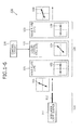
- Fig. 1-1 depicts a configuration example of an optical device according to an embodiment.
- an optical device 100 includes a light source unit 110, a liquid crystal device 120, and a control circuit 130.
- the light source unit 110 and the control circuit 130 may be disposed outside the optical device 100.
- the light source unit 110 emits laser light of a given wavelength in a given polarization state.
- Laser light is, for example, linearly polarized laser light that includes multiple beams of primary color light in terms of space or time.
- the light source unit 110 for example, includes an RGB laser light source 111 and a polarization-maintaining fiber 112.
- the RGB laser light source 111 emits linearly polarized laser light that includes multiple beams of primary color (red, green, and blue) light.
- the light source unit 110 is, for example, a light source unit that operates by the field sequential method to cause light sources for respective colors to emit light in a time-sharing sequence.
- the polarization-maintaining fiber 112 is a polarization maintaining fiber (PMF) that maintains the polarization state (linear polarization) of laser light emitted from the RGB laser light source 111 and that sends the laser light to the liquid crystal device 120.
- a polarization direction 101 represents the polarization direction (e.g., 0 degrees) of laser light emitted from the polarization-maintaining fiber 112 to the liquid crystal device 120.
- the liquid crystal device 120 includes a wave plate 121 serving as a second wave plate, a liquid crystal cell 123, and a wave plate 125.
- the wave plates 121 and 125 are, for example, quarter wave plates identical in configuration with one another.
- each of the wave plates 121 and 125 can be made out of a liquid crystal cell.
- the wave plate 121 transmits laser light emitted from the polarization-maintaining fiber 112.
- a slow axis orientation 122 represents the direction of the slow axis (phase delay axis) of the wave plate 121.
- the slow axis is the axis at which the refractive index of birefringence becomes the highest.
- the slow axis of the wave plate 121 is set at an angle of about 0 degrees with respect to the given polarization direction 101 of laser light emitted from the polarization-maintaining fiber 112.
- the wave plate 121 therefore, emits laser light passing therethrough to the liquid crystal cell 123 without changing the polarization state of the laser light.
- the liquid crystal cell 123 transmits laser light emitted from the wave plate 121.
- the liquid crystal cell 123 rotates the polarization direction of laser light passing therethrough, by a degree of rotation that can be shifted.
- a director direction 124 represents the direction of the director of a liquid crystal molecule. As indicated by the director direction 124, the angle of the director of the liquid crystal cell 123 with respect to the slow axis orientation 122 of the wave plate 121 can be shifted to about 67.5 degrees and to 112.5 degrees in a direction parallel with the substrate surface of the liquid crystal cell 123.
- the wave plate 125 transmits laser light emitted from the liquid crystal cell 123.
- a slow axis orientation 126 represents the direction of the slow axis (phase delay axis) of the wave plate 125. As indicated by the slow axis orientation 126, the slow axis of the wave plate 125 is set at an angle of about 0 degrees with respect to the polarization direction 101 of laser light emitted from the polarization-maintaining fiber 112. Laser light passing through the wave plate 125 is emitted to a device downstream of the optical device 100.
- Polarization states 102 and 103 represent the polarization directions of the laser light emitted from the wave plate 125.
- the director direction 124 of the liquid crystal cell 123 is shifted to 67.5 degrees with respect to the slow axis orientation 122, the laser light emitted from the wave plate 125 is in a state of counterclockwise circular polarization, as indicated by the polarization state 102.
- the director direction 124 of the liquid crystal cell 123 is shifted to 112.5 degrees with respect to the slow axis orientation 122, laser light emitted from the wave plate 125 is in a state of clockwise circular polarization, as indicated by the polarization state 103.
- the control circuit 130 cyclically shifts the angle of the director direction 124 of the liquid crystal cell 123 with respect to the slow axis orientation 122 of the wave plate 121, to 67.5 degrees and to 112.5 degrees.
- the control circuit 130 shifts the director direction 124 of the liquid crystal cell 123 by controlling the voltage applied to electrodes of the liquid crystal cell 123.
- the liquid crystal device 120 works as a quarter wave plate that changes the polarization state of laser light emitted from the polarization-maintaining fiber 112, to a circular polarization state.
- the director direction 124 of the liquid crystal cell 123 By shifting the director direction 124 of the liquid crystal cell 123, the polarization state of laser light emitted from the liquid crystal device 120 is changed alternately to the counterclockwise circular polarization state and to the clockwise circular polarization state.
- the liquid crystal cell 123 is disposed between the wave plate 121 and the wave plate 125.
- the liquid crystal device 120 is caused to work as the quarter wave plate for laser light emitted from the liquid crystal device 120, without dependency on the polarization state of the laser light incident on the liquid crystal device 120.
- Fig. 1-2 depicts a first modification of the optical device.
- components identical to those depicted in Fig. 1-1 are denoted by the same reference numerals used in Fig. 1-1 and are omitted in further description.
- the wave plate 121 may be omitted from the liquid crystal device 120, as shown in Fig. 1-2 .
- the same effect as that of the optical device 100 of Fig. 1-1 can be achieved and the number of components can be reduced.
- Fig. 1-3 depicts a second modification of the optical device.
- components identical to those depicted in Fig. 1-1 are denoted by the same reference numerals used in Fig. 1-1 and are omitted in further description.
- the director direction 124 of the liquid crystal cell 123 may also be shifted to 45 degrees and to 0 degrees with respect to the slow axis orientation 122.
- the liquid crystal device 120 works as a half wave plate.
- the wave plate 121 does not change the polarization state of incident laser light.
- the director direction 124 of the liquid crystal cell 123 is set at 45 degrees with respect to the slow axis orientation 122, the director direction 124 is tilted by +45 degrees with respect to the polarization direction 101 of laser light.
- the slow axis orientation 126 is tilted by +90 degrees with respect to the polarization direction of laser light from the liquid crystal cell 123, the wave plate 125 does not change the polarization state of laser light emitted from the liquid crystal cell 123.
- the liquid crystal cell 123 When the director direction 124 makes zero angle with respect to the polarization direction 101 of laser light, the liquid crystal cell 123 does not change the polarization direction of laser light emitted from the wave plate 121. Because the slow axis orientation 126 makes zero angle with respect to laser light from the liquid crystal cell 123, the wave plate 125 does not change the polarization state of laser light emitted from the liquid crystal cell 123.
- a polarization state 104 represents the polarization direction of laser light that is emitted from the liquid crystal device 120 when the director direction 124 of the liquid crystal cell 123 is set at 45 degrees with respect to the slow axis orientation 122.
- a polarization state 105 represents the polarization direction of laser light that is emitted from of the liquid crystal device 120 when the director direction 124 of the liquid crystal cell 123 makes zero angle with respect to the slow axis orientation 122.
- the polarization state of laser light emitted from the liquid crystal device 120 is shifted to zero-degree linear polarization and to 90-degree linear polarization with respect to the polarization direction 101.
- Fig. 1-4 depicts a third modification of the optical device.
- components identical to those depicted in Fig. 1-3 are denoted by the same reference numerals used in Fig. 1-3 and are omitted in further description.
- a case where the polarization state of laser light incident on the liquid crystal device 120 is assumed to be 45-degree linear polarization with respect to the slow axis orientation 122 will be described.
- the wave plate 121 changes the polarization state of incident laser light to a clockwise circular polarization state.
- the liquid crystal cell 123 changes the polarization direction of laser light emitted from the wave plate 121, to counterclockwise circular polarization.
- the wave plate 125 changes the polarization state of laser light emitted from the liquid crystal cell 123, to zero-degree linear polarization with respect to the laser light incident on the liquid crystal device 120, and transmits the linearly polarized laser light.
- Fig. 1-5 depicts a fourth modification of the optical device.
- components identical to those depicted in Fig. 1-3 are denoted by the same reference numerals used in Fig. 1-3 and are omitted in further description.
- a case where the polarization state of laser light incident on the liquid crystal device 120 is assumed to be 30-degree linear polarization with respect to the slow axis orientation 122 will be described.
- the wave plate 121 changes the polarization state of incident laser light to a clockwise elliptical polarization state (in which the major axis of the ellipse is parallel with the slow axis orientation 122).
- the liquid crystal cell 123 changes the polarization direction of laser light emitted from the wave plate 121, to a counterclockwise elliptical polarization state (in which the major axis of the ellipse is orthogonal to the slow axis orientation 122).
- the wave plate 125 cancels a phase shift of n/4 in the x-axis direction and the same in the y-axis direction. As a result, the wave plate 125 changes the polarization state of laser light emitted from the liquid crystal cell 123, to 60-degree linear polarization with respect to the slow axis orientation 122, and transmits the linearly polarized laser light.
- Fig. 1-6 depicts a fifth modification of the optical device.
- components identical to those depicted in Fig. 1-3 are denoted by the same reference numerals used in Fig. 1-3 and are omitted in further description.
- a case where the polarization state of laser light incident on the liquid crystal device 120 is assumed to be 60-degree linear polarization with respect to the slow axis orientation 122 will be described.
- the wave plate 121 changes the polarization state of incident laser light to a clockwise elliptical polarization state (in which the major axis of the ellipse is orthogonal with the slow axis orientation 122).
- the liquid crystal cell 123 changes the polarization direction of laser light emitted from the wave plate 121, to a counterclockwise elliptical polarization state (in which the major axis of the ellipse is parallel to the slow axis orientation 122).
- the wave plate 125 cancels a phase shift of n/4 in the x-axis direction and the same in the y-axis direction. As a result, the wave plate 125 changes the polarization state of laser light emitted from the liquid crystal cell 123, to 30-degree linear polarization with respect to the slow axis orientation 122, and transmits the linearly polarized laser light.
- Equation (1) An action by an ordinary wave plate on the polarization state of laser light can be expressed as, for example, equation (1) in the form of a Jones matrix.
- ⁇ e denotes a retardation (phase difference) by the wave plate
- ⁇ e denotes an azimuth
- (Vx, Vy) denotes incident polarization.
- the azimuth ⁇ of the liquid crystal cell 123 is the angle of the direction of the director (direction of the slow axis) of the liquid crystal cell 123 with respect to the direction of the slow axes of the wave plates 121 and 125.
- a Jones matrix for the liquid crystal device 120 composed of the wave plates 121 and 125 and the liquid crystal cell 123 is expressed as, for example, equation (2), in which "x" denotes the product of matrices.
- the retardations ⁇ 1 and have chromatic dispersion characteristics.
- the azimuth ⁇ e of the liquid crystal device 120 serving as a wave plate is determined to be n/4, regardless of the azimuth ⁇ between the slow axes of the wave plates 121 and 125 and the slow axis of the liquid crystal cell 123.
- Fig. 2-1 depicts an example of the characteristics of the retardation by the liquid crystal device.
- the horizontal axis represents the azimuth ⁇ between the slow axes of the wave plates 121 and 125 and the slow axis of the liquid crystal cell 123 and the vertical axis represents the retardation ⁇ e by the liquid crystal device 120.
- Retardation characteristics 210 represent the characteristics of the retardation ⁇ e to the azimuth ⁇ .
- the retardation ⁇ e by the liquid crystal device 120 changes from 0 to 2n corresponding to the azimuth ⁇ between the slow axes of the wave plates 121 and 125 and the slow axis of the liquid crystal cell 123.
- the liquid crystal device 120 works as the half wave plate whose slow axis is adjusted to 45 degrees with respect to incident polarization.
- the azimuth ⁇ is 3n/8
- the retardation ⁇ e is n/2.
- the liquid crystal device 120 works as the quarter wave plate whose slow axis is adjusted to 45 degrees with respect to incident polarization.
- Fig. 2-2 depicts an example of the chromatic dispersion characteristics of the liquid crystal device of Fig. 1-1 .
- the horizontal axis represents the wavelength [nm] of the light and the vertical axis represents the phase difference (retardation) by the liquid crystal device 120 due to birefringence.
- the chromatic dispersion characteristics 201 are indicated as reference data representing the characteristics of phase differences for wavelengths shown by laser light having passed through an ordinary quarter wave plate.
- the phase difference ⁇ of laser light having passed through an ordinary quarter wave plate can be expressed by, for example, equation (8).
- ⁇ 2 ⁇ ⁇ / ⁇ ⁇ ne - no ⁇ d
- ⁇ denotes the wavelength of the light
- ne denotes the refractive index along the direction of a fast axis (phase advance axis) of the quarter wave plate, where the fast axis is the axis at which a refractive index in birefringence is the lowest
- no denotes the refractive index along the direction of the slow axis of the quarter wave plate
- d denotes the thickness of the quarter wave plate.
- the chromatic dispersion characteristics 201 represent characteristics that vary the phase difference ⁇ according to the wavelength ⁇ .
- ⁇ denotes the angle of the director direction 124 of the liquid crystal cell 123 with respect to the slow axes of the wave plates 121 and 125.
- the liquid crystal device 120 works as a quarter wave plate with low wavelength dependency (i.e., quarter wave plate applicable to wide wavelength bands). According to the optical device 100, therefore, the polarization state of laser light can be controlled as chromatic dispersion is suppressed. Because chromatic dispersion is suppressed, a drop in the extinction ratio is suppressed, which improves the quality of an image created on a screen by projecting the laser light thereon.
- the polarization state of laser light that includes multiple beams of primary color light can be controlled by the liquid crystal device 120.
- the number of components is reduced, compared to, for example, a case of providing a polarization controller for each primary color light, thereby enabling a reduction in the size of the device.
- the liquid crystal cell 123 may be made of, for example, a nematic liquid crystal, or made of a ferroelectric liquid crystal (FLC).
- the liquid crystal cell 123 may be provided as a liquid crystal cell having multiple electrodes that maintain director directions that are different from one another (see, e.g., Figs. 8-1 to 8-4 ).
- Each of the above liquid crystal cells shifts the direction of the director of a liquid crystal molecule by rotating the direction parallel to the substrate surface, and can control the movement of the liquid crystal molecule by only the field response rate of the liquid crystal, using a horizontal electric field.
- Each liquid crystal cell therefore, can shift the polarization state of laser light at high speed. Shifting the polarization state of laser light at high speed improves the effect of speckle reduction and enables generation of a three-dimensional image with a high frame rate.
- the light source unit combines multiple beams of laser light differing in wavelength from one another, into a single beam of laser light.
- Fig. 3-1 depicts a configuration example of the light source unit.
- the light source unit 110 of Fig. 1-1 has, for example, a red light source 311, a green light source 312, a blue light source 313, polarization-maintaining fibers 314 to 316, a combiner 317, and a polarization-maintaining fiber 318, as depicted in Fig. 3-1 .
- the polarization-maintaining fiber 318 corresponds to the polarization-maintaining fiber 112 of Fig. 1-1 .
- the red light source 311 (R) oscillates to emit red laser light to the polarization-maintaining fibers 314.
- the green light source 312 (G) oscillates to emit green laser light to the polarization-maintaining fibers 315.
- the blue light source 313 (B) oscillates to emit blue laser light to the polarization-maintaining fibers 316. It is assumed that the polarization states of beams of laser light emitted respectively from the red light source 311, the green light source 312, and the blue light source 313 are a state of linear polarization in a given direction.
- the red light source 311, the green light source 312, and the blue light source 313 may be provided respectively as, for example, a laser device that directly emits each color of laser light or as a second harmonic generation (SHG) laser device.
- the polarization-maintaining fiber 314 maintains the polarization state of laser light emitted from the red light source 311 and emits the laser light to the combiner 317.
- the polarization-maintaining fiber 315 maintains the polarization state of laser light emitted from the green light source 312 and emits the laser light to the combiner 317.
- the polarization-maintaining fiber 316 maintains the polarization state of laser light emitted from the blue light source 313 and emits the laser light to the combiner 317.
- the combiner 317 is a light-combining unit that combines beams of laser light emitted from the polarization-maintaining fibers 314 to 316.
- the combiner 317 emits combined laser light to the polarization-maintaining fiber 318, which maintains the polarization state of laser light emitted from the combiner 317 and emits the laser light.
- laser light emitted from the polarization-maintaining fiber 318 is laser light that includes beams of red, green, and blue color light.
- the polarization state of laser light emitted from the polarization-maintaining fiber 318 is a state of linear polarization in a given direction.
- Fig. 3-2 depicts a first modification of the light source unit.
- components identical to those depicted in Fig. 3-1 are denoted by the same reference numerals used in Fig. 3-1 and are omitted in further description.
- the light source unit 110 may have the red light source 311, the green light source 312, the blue light source 313, a mirror 321, and dichroic mirrors 322 and 323.
- the red light source 311 oscillates to emit red laser light to the mirror 321.
- the green light source 312 oscillates to emit green laser light to the dichroic mirror 322.
- the blue light source 313 oscillates to emit blue laser light to the dichroic mirror 323.
- the mirror 321 reflects laser light emitted from the red light source 311 and sends the laser light to the dichroic mirror 322.
- the dichroic mirrors 322 and 323 are light-combining units that combine beams of laser light emitted from the red light source 311, the green light source 312, and the blue light source 313.
- the dichroic mirror 322 reflects and outputs to the dichroic mirror 323, laser light (light having a wavelength for green) emitted from the green light source 312.
- the dichroic mirror 322 transmits and outputs to the dichroic mirror 323, laser light (light having a wavelength for red) emitted from the mirror 321.
- the dichroic mirror 323 reflects and outputs to a device downstream of the light source unit 110, laser light (light having a wavelength for blue) emitted from the blue light source 313.
- the dichroic mirror 323 transmits and outputs to the device downstream of the light source unit 110, laser light (beams of light having wavelengths for red and green) emitted from the dichroic mirror 322.
- Each of the dichroic mirrors 322 and 323 can be implemented by using, for example, a dielectric multilayer film.
- Laser light emitted from the dichroic mirror 323 is laser light that includes beams of red, green, and blue color light.
- the polarization state of laser light emitted from the dichroic mirror 323 is a state of linear polarization in a given direction.
- Fig. 3-3 depicts a second modification of the light source unit.
- the light source unit 110 may have the red light source 311, the green light source 312, the blue light source 313, and the dichroic mirrors 322 and 323.
- the red light source 311 oscillates to emit red laser light to the dichroic mirror 322.
- the green light source 312 oscillates to emit green laser light to the dichroic mirror 322.
- the blue light source 313 oscillates to emit blue laser light to the dichroic mirror 323.
- the dichroic mirror 322 reflects and outputs to the dichroic mirror 323, laser light (light having a wavelength for red) emitted from the red light source 311.
- the dichroic mirror 322 transmits and outputs to the dichroic mirror 323, laser light (light having a wavelength for green) emitted from the green light source 312.
- the dichroic mirror 323 reflects and outputs to a device downstream of the light source unit 110, laser light (light having a wavelength for blue) emitted from the blue light source 313.
- the dichroic mirror 323 transmits and outputs to the device downstream of the light source unit 110, laser light (beams of light having wavelengths for red and green) emitted from the dichroic mirror 322.
- Laser light emitted from the dichroic mirror 323 is laser light that includes beams of red, green, and blue color light.
- the polarization state of laser light emitted from the dichroic mirror 323 is a state of linear polarization in a given direction.
- FIG. 4-1 depicts a first configuration example of a video engine to which the optical device is applied.
- a video engine 400 of Fig. 4-1 is a video engine to which the optical device 100 of Fig. 1-1 is applied and in which a liquid crystal on silicon (LCOS) is used.
- the video engine 400 includes the light source unit 110, a lens 410, a polarizing beam splitter 420, an LCOS 430, a lens 440, and the liquid crystal device 120.
- LCOS liquid crystal on silicon
- the lens 410 emits incoming laser light from the light source unit 110 to the polarizing beam splitter 420.
- the polarizing beam splitter 420 reflects incoming laser light from the lens 410 and sends the reflected light to the LCOS 430.
- the polarizing beam splitter 420 emits incoming laser light from the LCOS 430 to the lens 440 according to the polarization state of the laser light.
- the LCOS 430 is a modulator that modulates laser light spatially to generate video.
- the LCOS 430 reflects incoming laser light from the polarizing beam splitter 420 back to the polarizing beam splitter 420.
- the LCOS 430 controls the polarization state of the reflected light at each pixel.
- the intensity of laser light passing through the polarizing beam splitter 420 and falling onto the lens 440 can be controlled for each pixel.
- the lens 440 condenses incoming laser light from the polarizing beam splitter 420 and emits the condensed laser light to the liquid crystal device 120.
- the lens 440 may be configured by combining multiple lenses together.
- the liquid crystal device 120 controls the polarization state of incoming laser light from the lens 440 and emits the laser light to a device downstream. Laser light emitted from the liquid crystal device 120 is projected onto, for example, a screen.
- Fig. 4-2 depicts a modification of the first configuration example of the video engine.
- components identical to those depicted in Fig. 4-1 are denoted by the same reference numerals used in Fig. 4-1 and are omitted in further description.
- an FLC is used as the liquid crystal cell 123
- light having passed through the polarizing beam splitter 420 does not have to be condensed.
- reflected light from the LCOS 430 may be projected without being condensed.
- FIG. 5-1 depicts a second configuration example of a video engine to which the optical device is applied.
- a video engine 500 of Fig. 5-1 is a video engine to which the optical device 100 of Fig. 1-1 is applied and in which a micro electro mechanical system (MEMS) is used.
- the video engine 500 includes the light source unit 110, a lens 510, the liquid crystal device 120, and an MEMS mirror 520.
- the lens 510 emits incoming laser light from the light source unit 110 to the liquid crystal device 120.
- the liquid crystal device 120 controls the polarization state of incoming laser light from the lens 510 and sends the laser light to the MEMS mirror 520.
- the lens 510 may be configured by combining multiple lenses together.
- the MEMS mirror 520 is a modulator that modulates laser light spatially to generate video.
- the MEMS mirror 520 has a mirror 521 and rotating shafts 522 and 523.
- the mirror 521 reflects incoming laser light from the liquid crystal device 120.
- the mirror 521 rotates about each of the rotating shafts 522 and 523 under external control.
- the rotating shafts 522 and 523 are the rotating shafts set at different angles to each other (e.g., at right angles to each other).
- the mirror 521 therefore, reflects laser light at various angles. Hence, laser light reflected by the mirror 521 scan the screen surface.
- Fig. 5-2 depicts a third configuration example of a video engine to which the optical device is applied.
- components identical to those depicted in Fig. 1-1 or Fig. 5-1 are denoted by the same reference numerals used in Fig. 5-1 and are omitted in further description.
- a video engine 500 of Fig. 5-2 is a modification of the video engine 500 of Fig. 5-1 .
- the video engine 500 includes the light source unit 110, a polarization-maintaining fiber 530, a collimator lens 541, the liquid crystal device 120, a collimator lens 543, a polarization-maintaining fiber 550, a collimator lens 560, and the MEMS mirror 520.
- the polarization-maintaining fiber 530 maintains the polarization state of laser light emitted from the light source unit 110 and sends the laser light to the collimator lens 541.
- the collimator lens 541 collimates incoming laser light from the polarization-maintaining fiber 530 and emits the collimated laser light to the liquid crystal device 120.
- the collimator lens 541 is fixed to the liquid crystal device 120 by resin 542.
- the liquid crystal device 120 controls the polarization state of laser light emitted from the collimator lens 541 and sends the laser light to the collimator lens 543.
- the collimator lens 543 optically couples laser light emitted from the liquid crystal device 120, to the polarization-maintaining fiber 550.
- the collimator lens 543 is fixed to the liquid crystal device 120 by resin 544.
- the polarization-maintaining fiber 550 maintains the polarization state of laser light optically coupled to the polarization-maintaining fiber 550 by the collimator lens 543 and sends the laser light to the collimator lens 560.
- the collimator lens 560 emits incoming laser light from the polarization-maintaining fiber 550 to the MEMS mirror 520.
- the MEMS mirror 520 reflects incoming laser light from the collimator lens 560 at various angles.
- FIG. 6-1 depicts a fourth configuration example of a video engine to which the optical device is applied.
- a video engine 600 of Fig. 6-1 is a video engine to which the optical device 100 of Fig. 1-1 is applied and in which a digital light processing (DLP: registered trademark) is used.
- the video engine 600 includes the light source unit 110, the liquid crystal device 120, a lens 610, and a DLP 620.
- the liquid crystal device 120 controls the polarization state of incoming laser light from the light source unit 110 and sends the laser light to the lens 610.
- the lens 610 emits incoming laser light from the liquid crystal device 120 to the DLP 620.
- the lens 610 may be configured by combining multiple lenses together.
- the DLP 620 is a modulator that modulates laser light spatially to generate video.
- the DLP 620 reflects incoming laser light from the lens 610 toward a screen.
- the DLP 620 controls the reflection angle of light for each pixel on a surface that reflects laser light. Through this control, for each pixel of the DLP 620, light is reflected to the screen or in a direction different from the direction of the screen. As a result, the intensity of laser light projected onto the screen can be controlled for each pixel.
- Fig. 6-2 depicts a fifth configuration example of a video engine to which the optical device is applied.
- components identical to those depicted in Figs. 1-1 , 5-2 , or 6-1 are denoted by the same reference numerals used in Figs. 1-1 , 5-2 , and 6-1 , and are omitted in further description.
- a video engine 600 of Fig. 6-2 is a modification of the video engine 600 of Fig. 6-1 .
- the video engine 600 includes the light source unit 110, the polarization-maintaining fiber 530, the collimator lens 541, the liquid crystal device 120, the collimator lens 543, the polarization-maintaining fiber 550, the collimator lens 560, and the DLP 620.
- the collimator lens 560 emits laser light to the DLP 620.
- the DLP unit reflects incoming laser light from the collimator lens 560 at various angles at respective pixels.
- the liquid crystal device 120 merely has to adjust a single beam of laser light created by combining beams of laser light at the light source unit.
- the video engine can be reduced in overall size and can be adjusted easily.
- FIG. 7 depicts a configuration example of a projector to which the optical device is applied.
- components identical to those depicted in Figs. 1-1 , 3-1 to 3-3 , 4-1 , etc., are denoted by the same reference numerals used in Figs. 1-1 , 3-1 to 3-3 , 4-1 , etc., and are omitted in further description.
- a projector 700 of Fig. 7 includes a video engine 710, a control board 720, and a power supply 730.
- the video engine 710 may be provided as, for example, the video engine 400 of Fig. 4-1 , the video engine 500 of Figs. 5-1 and 5-2 , or the video engine 600 of Figs. 6-1 and 6-2. A case of using the video engine 400 of Fig. 4-1 as the video engine 710 will be described.
- the video engine 710 includes the red light source 311, the green light source 312, the blue light source 313, the liquid crystal device 120, and the LCOS 430.
- the control board 720 has a light source controller 721, a liquid crystal element controller 722, an LCOS controller 723, and a control unit 724. Under the control of the control unit 724, the light source controller 721 controls a drive current supplied to the red light source 311, the green light source 312, and the blue light source 313 and thereby, controls beams of light emitted from the red light source 311, the green light source 312, and the blue light source 313, respectively.
- the liquid crystal element controller 722 corresponds to the control circuit 130 of Fig. 1-1 . Under the control of the control unit 724, the liquid crystal element controller 722 controls the voltage applied to electrodes of the liquid crystal cell 123 and thereby, controls the polarization state of laser light emitted out of the projector 700. For example, the liquid crystal element controller 722 cyclically shifts the angle of the director direction 124 of the liquid crystal cell 123 with respect to the slow axis orientation 122 of the wave plate 121, to 67.5 degrees and to 112.5 degrees.
- the control unit 724 has a video signal processing unit 725.
- the video signal processing unit 725 performs video processing based on a video signal input to the projector 700. Based on the video processing by the video signal processing unit 725, the control unit 724 controls the light source controller 721, the liquid crystal element controller 722, and the LCOS controller 723.
- the LCOS controller 723 modulates laser light by controlling the voltage applied to electrodes of the LCOS 430 and thereby, controls images and video created by laser light emitted from the projector 700. Hence, laser light from the projector 700 is projected onto a screen to display video images.
- the power supply 730 is the power supply to the control board 720.
- the power supply 730 may be a battery.
- Fig. 8-1 depicts a first example of the electrode structure of the liquid crystal cell.
- the liquid crystal cell 123 of Fig. 8-1 is the liquid crystal cell 123 as viewed in the traveling direction of laser light (the same applies to the liquid crystal cell 123 of Figs. 8-2 to 8-4 ).
- Electrodes 811 to 818 are electrodes of the liquid crystal cell 123.
- the electrodes 811 to 818 are set at angles of 0 degrees, 45 degrees, 90 degrees, 135 degrees, 180 degrees, 225 degrees, 270 degrees, and 315 degrees, respectively.
- the electrodes 811 and 815, the electrodes 812 and 816, the electrodes 813 and 817, and the electrodes 814 and 818 are paired, respectively.
- the application of voltage to paired electrodes causes the director of a liquid crystal molecule in the liquid crystal cell 123 to rotate parallel to the substrate surface, whereby the director direction is controlled.
- the director direction of the liquid crystal cell 123 can be controlled to be 0 degrees.
- Voltage may be applied to electrodes other than the paired electrodes. In this manner, by balancing the voltage applied to respective electrodes, the director direction of the liquid crystal cell 123 can be controlled over a broader range. In this manner, because the movement of the liquid crystal molecule can be controlled through only the field response rate of the liquid crystal, the liquid crystal cell 123 can be operated at high speed.
- the polarization direction of laser light incident on the liquid crystal device 120 and the slow axis orientations 122 and 126 of the wave plates 121 and 125 are set to any one among directions of 22.5 degrees, 67.5 degrees, 112.5 degrees, and 157.5 degrees, as indicated by polarization directions 810.
- the angle of the director direction of the liquid crystal cell 123 can be shifted to 67.5 degrees and to 112.5 degrees with respect to the slow axis orientations 122 and 126 of the wave plates 121 and 125.
- liquid crystal polarization controlling device described in non-patent document ( Yasuo OHTERA, Takafumi CHIBA, and Shojiro KAWAKAMI, "Liquid Crystal Polarization Controlling Devices Utilizing Rotating Electric Fields", Optics, Vol. 30, 1st issue, pp. 29-30, January 10, 2001 ) can be used as the liquid crystal cell 123 of Fig. 8-1 .
- Fig. 8-2 depicts a second example of the electrode structure of the liquid crystal cell.
- Electrodes 821 to 824 of Fig. 8-2 are electrodes of the liquid crystal cell 123.
- the electrodes 821 to 824 are set at angles of 45 degrees, 90 degrees, 225 degrees, and 270 degrees, respectively. Because the liquid crystal cell 123 has to shift the director direction thereof to two directions of 67.5 degrees and 112.5 degrees, the liquid crystal cell 123 are to be provided with two pairs of electrodes, as depicted in Fig. 8-2 .
- the polarization direction of laser light incident on the liquid crystal device 120 and the slow axis orientations 122 and 126 of the wave plates 121 and 125 are set to any one among directions of 22.5 degrees, 67.5 degrees, 112.5 degrees, and 157.5 degrees, as indicated by polarization directions 820.
- the angle of the director direction of the liquid crystal cell 123 can be shifted to 67.5 degrees and to 112.5 degrees with respect to the slow axis orientations 122 and 126 of the wave plates 121 and 125.
- Fig. 8-3 depicts a third example of the electrode structure of the liquid crystal cell. Electrodes 831 to 834 of Fig. 8-3 are electrodes of the liquid crystal cell 123. The electrodes 831 to 834 are set at angles of 0 degrees, 90 degrees, 180 degrees, and 270 degrees, respectively.
- the polarization direction of laser light incident on the liquid crystal device 120 and the slow axis orientations 122 and 126 of the wave plates 121 and 125 are set to any one among directions of 22.5 degrees, 67.5 degrees, 112.5 degrees, and 157.5 degrees, as indicated by polarization directions 830.
- the angle of the director direction of the liquid crystal cell 123 can be shifted to 67.5 degrees and to 112.5 degrees with respect to the slow axis orientations 122 and 126 of the wave plates 121 and 125.
- Electrodes 841 to 848 are electrodes of the liquid crystal cell 123.
- the electrodes 841 to 848 are set at angles of 22.5 degrees, 67.5 degrees, 112.5 degrees, 157.5 degrees, 202.5 degrees, 247.5 degrees, 292.5 degrees, and 337.5 degrees, respectively.
- the electrodes 841 to 848 are obtained by tilting the electrodes 811 to 818 of Fig. 8-1 by 22.5 degrees, respectively.
- the polarization direction of laser light incident on the liquid crystal device 120 and the slow axis orientations 122 and 126 of the wave plates 121 and 125 are set to any one among directions of 0 degrees, 45 degrees, 90 degrees, and 135 degrees, as indicated by polarization directions 840.
- the angle of the director direction of the liquid crystal cell 123 can be shifted to 67.5 degrees and to 112.5 degrees with respect to the slow axis orientations 122 and 126 of the wave plates 121 and 125.
- the liquid crystal cell 123 has multiple pairs of electrodes that maintain director directions and therefore, can shift multiple director directions at high speed.
- the liquid crystal cell 123 has first electrodes that keep the direction of directors at 67.5 degrees with respect to the direction of the slow axes of the wave plates 121 and 125, and second electrodes that keep the direction of directors at 112.5 degrees with respect to the direction of the slow axes of the wave plates 121 and 125.
- Fig. 9-1 depicts a first example of the form of use of the projector.
- the projector 700 of Fig. 9-1 is, for example, the projector 700 of Fig. 7 .
- the projector 700 emits laser light 901 onto a screen 920 while causing the optical device 100 to cyclically change the polarization states at high speed. As a result, speckles of video and images projected on the screen 920 are reduced and image quality is improved.
- Fig. 9-2 depicts a second example of the form of use of the projector.
- components identical to those depicted in Fig. 9-1 are denoted by the same reference numerals used in Fig. 9-1 and are omitted in further description.
- the projector 700 alternately emits laser light 902 in a counterclockwise circular polarization state and laser light 903 in a clockwise circular polarization state, onto the screen 920.
- Each of laser light 902 and laser light 903 is modulated so as to create images seen from different points of view.
- a pair of three-dimensional glasses 930 has a glass 931 that transmits only the laser light 902 in a counterclockwise circular polarization state and a glass 932 that transmits only the laser light 903 in a clockwise circular polarization state.
- the three-dimensional glasses 930 allows a person wearing the three-dimensional glasses 930 to visually perceive a three-dimensional image. While the configuration for realizing a three-dimensional image by switching circular polarization states is described in this example, a configuration for realizing a three-dimensional image by switching linear polarization states in different directions is also be possible.
- Fig. 10 is a flowchart of an example of control in a case of realizing a reduction in speckles.
- the optical device 100 under control of the control unit 724 executes, for example, steps depicted in Fig. 10 .
- the liquid crystal element controller 722 shifts the director direction 124 of the liquid crystal cell 123 (step S1001).
- the LCOS controller 723 inputs a video signal for red to the LCOS 430 (step S1002).
- the light source controller 721 then turns on the red light source 311 (step S1003).
- the light source controller 721 then turns off the red light source 311 (step S1004).
- the LCOS controller 723 inputs a video signal for green to the LCOS 430 (step S1005).
- the light source controller 721 then turns on the green light source 312 (step S1006).
- the light source controller 721 then turns off the green light source 312 (step S1007).
- the LCOS controller 723 inputs a video signal for blue to the LCOS 430 (step S1008).
- the light source controller 721 then turns on the blue light source 313 (step S1009).
- the light source controller 721 then turns off the blue light source 313 (step S1010), and the process flow returns to step S1001.
- polarization states are changed by shifting the director direction 124 of the liquid crystal cell 123 as beams of laser light bearing different colors are output in time-sharing sequence.
- the director direction 124 of the liquid crystal cell 123 can be shifted.
- shifting of the director direction 124 of the liquid crystal cell 123 does not need to be synchronized with the control of the red light source 311, the green light source 312, the blue light source 313, and the LCOS 430.
- Fig. 11 depicts an example of the shifting of the director direction of the liquid crystal device.
- components identical to those depicted in Fig. 8-1 are denoted by the same reference numerals used in Fig. 8-1 and are omitted in further description.
- a director 1110 is the director of the liquid crystal cell 123.
- States 1101 to 1104 represent states of the shifting of the direction of the director 1110.
- the liquid crystal element controller 722 shifts the direction of the director 1110 by 45 degrees at each execution of step S1001 in Fig. 10 .
- the direction of the director 1110 can be shifted sequentially to the direction in the state 1101, the direction in the state 1102, the direction in the state 1103, the direction in the state 1104, the direction in the state 1101, and so on.
- Fig. 12 is a flowchart of an example of control in a case of realizing a three-dimensional image. For example, when a three-dimensional image is realized by the optical device 100 as in the example of Fig. 9-2 , steps depicted in Fig. 12 are executed repeatedly, for example, under the control of the control unit 724.
- the liquid crystal element controller 722 shifts the director direction 124 of the liquid crystal cell 123 (step S1201). Subsequently, the light source controller 721 turns off the blue light source 313 (step S1202). The light source controller 721 then turns on the red light source 311 (step S1203).
- the LCOS controller 723 inputs a red color video signal for the right eye, to the LCOS 430 (step S1204).
- the liquid crystal element controller 722 shifts the director direction 124 of the liquid crystal cell 123 (step S1205).
- the LCOS controller 723 then inputs a red color video signal for the left eye, to the LCOS 430 (step S1206).
- the liquid crystal element controller 722 shifts the director direction 124 of the liquid crystal cell 123 (step S1207).
- the light source controller 721 turns off the red light source 311 (step S1208).
- the light source controller 721 then turns on the green light source 312 (step S1209).
- the LCOS controller 723 inputs a green color video signal for the right eye, to the LCOS 430 (step S1210).
- the liquid crystal element controller 722 shifts the director direction 124 of the liquid crystal cell 123 (step S1211).
- the LCOS controller 723 then inputs a green color video signal for the left eye, to the LCOS 430 (step S1212).
- the liquid crystal element controller 722 shifts the director direction 124 of the liquid crystal cell 123 (step S1213).
- the light source controller 721 turns off the green light source 312 (step S1214).
- the light source controller 721 then turns on the blue light source 313 (step S1215).
- the LCOS controller 723 inputs a blue color video signal for the right eye, to the LCOS 430 (step S1216).
- the liquid crystal element controller 722 shifts the director direction 124 of the liquid crystal cell 123 (step S1217).
- the LCOS controller 723 then inputs a blue color video signal for the left eye, to the LCOS 430 (step S1218), and returns to step S1201.
- shifting of the director direction 124 of the liquid crystal cell 123 is synchronized with control over the red light source 311, the green light source 312, the blue light source 313, and the LCOS 430.
- shifting of the director direction 124 of the liquid crystal cell 123 is performed in synchronization with switching between a video signal for the right eye and a video signal for the left eye.
- the order of shifting of the director direction 124 of the liquid crystal cell 123 is, for example, the same as the order indicated in the example of Fig. 11 .
- Fig. 13-1 depicts an example of applied voltages to the liquid crystal cell.
- components identical to those depicted in Fig. 8-1 are denoted by the same reference numerals used in Fig. 8-1 and are omitted in further description.
- voltages applied to the electrodes 811 to 818 are assumed to be V 0 , V 0 /2(1+1 ⁇ 2), V 0 /2, V 0 /2(1-1 ⁇ 2), 0, V 0 /2(1-1 ⁇ 2), V 0 /2, and V 0 /2(1+1 ⁇ )2), respectively.
- the time for applying an applied voltage V to each of the electrodes 811 to 818 during one cycle can be calculated by, for example, equation (9).
- V 1 T ⁇ V 0 2 ⁇ dt
- Fig. 13-2 depicts an example of times for applying voltages during one cycle.
- electrodes 1 to 8 represent the electrodes 811 to 818, respectively.
- voltages applied to the electrodes 811 to 818 are determined to be V 0 , 0.854V 0 , 0.5V 0 , 0.146V 0 , 0, 0.146V 0 , 0.5V 0 , and 0.854V 0 , respectively.
- Times for applying applied voltages V to the electrodes 811 to 818 during one cycle are assumed to be T, 730T/1000, 250T/1000, 20T/1000, 0, 20T/1000, 250T/1000, and 730T/1000, respectively.
- Fig. 14-1 depicts a first example of the waveforms of voltages applied to the liquid crystal cell.
- the electrodes 1 to 8 represent the electrodes 811 to 818, respectively.
- Waveforms 1411 to 1418 represent the waveforms of respective voltages applied to the electrodes 811 to 818.
- Pulses 1 to 5 represent the waveform patterns of the applied voltages. For example, voltages of the same waveform pattern (pulse 2) are applied to the electrodes 812 and 818, respectively. Voltages of the same waveform pattern (pulse 3) are applied to the electrodes 813 and 817, respectively. Voltages of the same waveform pattern (pulse 4) are applied to the electrodes 814 and 816, respectively.
- the liquid crystal element controller 722 applies the voltages of the waveforms 1411 to 1418 to the electrodes 811 to 818, respectively, and thereby shifts the director direction of the liquid crystal cell 123 sequentially.
- Fig. 14-2 depicts a second example of the waveforms of voltages applied to the liquid crystal cell.
- the liquid crystal element controller 722 may apply voltages of waveforms 1411 to 1418 depicted in Fig. 14-2 to the electrodes 811 to 818 of the liquid crystal cell 123, respectively, and thereby, shift the director direction of the liquid crystal cell 123 sequentially.
- Fig. 15-1 depicts an example of voltages applied to the liquid crystal cell.
- parts identical to those depicted in Fig. 8-1 are denoted by the same reference numerals used in Fig. 8-1 and are omitted in further description.
- voltages applied to the electrodes 811 to 818 are assumed to be, for example, V 0 , V 0 / ⁇ 2, 0, -V 0 / ⁇ 2, - V 0 , -V 0 / ⁇ 2, 0, and V 0 / ⁇ 2, respectively. According to the above voltage application method, these voltages are to be applied to the electrodes 811 to 818 during 1/8 cycle.
- Fig. 15-2 depicts an example of times for applying voltages during one cycle.
- the electrodes 1 to 8 represent the electrodes 811 to 818, respectively.
- voltages applied to the electrodes 811 to 818 are assumed to be V 0 , 0.0707V 0 , 0, -0.707V 0 , -V 0 , -0.707V 0 , 0, and 0.707V 0 , respectively.
- Fig. 16 depicts a third example of the waveforms of voltages applied to the liquid crystal cell.
- the electrodes 1 to 8 represent the electrodes 811 to 818, respectively.
- Waveforms 1601 to 1608 represent the waveforms of respective voltages applied to the electrodes 811 to 818.
- Pulses 1 to 8 represent the waveform patterns of the applied voltages. For example, voltages applied to the electrodes 811 to 818 are determined to be V 0 , 0.070V 0 , 0, -0.707V 0 , -V 0 , -0.707V 0 , 0, and 0.707V 0 , respectively.
- Fig. 17 is a diagram (1) showing an example of electric field distribution generated by voltage application to the liquid crystal cell.
- Electric field distribution 1700 depicted in Fig. 17 represents electric field distribution that is generated on the substrate surface of the liquid crystal cell 123 when the above voltages (e.g., voltages depicted in Fig. 14-1 or Fig. 16 ) are applied to the liquid crystal cell 123.
- Areas 1701 to 1710 represent areas in which field intensities are 9 to 10, 8 to 9, 7 to 8, 6 to 7, 5 to 6, 4 to 5, 3 to 4, 2 to 3, 1 to 2, and 0 to 1, respectively.
- a director direction 1720 represents the direction of the director 1110
- Fig. 18 is a diagram (2) showing an example of electric field distribution generated by voltage application to the liquid crystal cell.
- parts identical to those depicted in Fig. 17 are denoted by the same reference numerals used in Fig. 17 and are omitted in further description.
- An electric field distribution 1800 of Fig. 18 represents an electric field distribution generated on the bulk of the liquid crystal cell 123 when the above voltages (e.g., voltages depicted in Fig. 14-2 ) are applied to the liquid crystal cell 123.
- Fig. 19 depicts an example of voltage application patterns for respective electrodes of the liquid crystal cell.
- parts identical to those depicted in Fig. 14-1 are denoted by the same reference numerals used in Fig. 14-1 and are omitted in further description.
- a table 1900 depicted in Fig. 19 indicates an example of voltage application patterns for the electrodes 811 to 818 of the liquid crystal cell 123. As indicated in the table 1900, at each cycle, the liquid crystal element controller 722 shifts pulses applied to the electrodes 811 to 818.
- the liquid crystal element controller 722 applies pulses 1, 2, 3, 4, 5, 4, 3, and 2 to the electrodes 811 to 818, respectively, at the first cycle and applies pulses 2, 3, 4, 5, 4, 3, 2 and 1 to the electrodes 811 to 818, respectively, at the second cycle. After ending the eighth cycle, the liquid crystal element controller 722 returns to the first cycle.
- Figs. 20-1 and 20-8 depict examples of changes of electric field distributions caused by voltage application patterns.
- components identical to those depicted in Fig. 17 are denoted by the same reference numerals used in Fig. 17 and are omitted in further description.
- Electric field distributions 2001 to 2008 of Figs. 20-1 to 20-8 represent the electric field distributions of the liquid crystal cell 123 at the first to eighth cycles indicated in the table 1900 of Fig. 19 , respectively.
- pulses applied to the electrodes 811 to 818 are changed at each cycle to change the electric field distributions of the liquid crystal cell 123.
- the director direction 124 of the liquid crystal cell 123 can be changed in sequence.
- Fig. 21 depicts another modification of the optical device.
- the optical device 100 may include the liquid crystal cell 123 as a reflective liquid crystal cell.
- the wave plates 121 and 125 of Fig. 1-1 are integrated into one wave plate 121.
- a mirror 1010 is disposed on the face of the liquid crystal cell 123 opposite to the face of the same closer to the wave plate 121.
- the liquid crystal cell 123 causes the mirror 1010 to reflect laser light of which the direction of polarization is rotated and emits the laser light to the wave plate 121.
- laser light reciprocates through the liquid crystal cell 123, in which process the polarization direction of reflected laser light is rotated by the liquid crystal cell 123 at the same degree as the degree of rotation of the polarization direction of laser light coming from the polarization-maintaining fiber 112 and incident on the liquid crystal cell 123.
- reciprocating laser light travels a light path that is twice the light path that the laser light travels when passing through just the liquid crystal cell 123.
- the liquid crystal cell 123 substantially functions as the half wave plate.
- the wave plate 121 transmits laser light emitted from the liquid crystal cell 123.
- the polarization state of reflected laser light having been reflected by the liquid crystal cell 123 and passed through the wave plate 121 becomes one of the polarization states 102 and 103 (see, Fig. 1-1 ).
- the liquid crystal cell 123 serves as the reflective liquid crystal cell and laser light is caused to reciprocate through the wave plate 121, achieving the same effect as that of the optical device 100 depicted in Fig. 1-1 .
- a configuration that omits the wave plate 125 becomes possible.
- the number of components can be reduced, enabling reduction of the device size.
- Laser light reflected by the liquid crystal cell 123 and passing through the wave plate 121 can be extracted by using, for example, a circulator. Laser light may be extracted by adjusting the angles of elements so that a position at which laser light from the light source unit 110 falls onto the wave plate 121 is different from a position at which laser light reflected by the liquid crystal cell 123 exits of the wave plate 121.
- the modification depicted in Fig. 21 is further applicable to, for example, the optical device 100 depicted in Figs. 1-2 , 1-3 , and 1-6 .
- Fig. 22 depicts an example of the operation of a laminated wave plate.
- components identical to those depicted in Fig. 1-1 are denoted by the same reference numerals used in Fig. 1-1 and are omitted in further description.
- the x axis corresponds to the above given direction (0 degrees)
- the z axis corresponds to the traveling direction of light. It is assumed that the retardations of the wave plates 121 and 125 are the same, ⁇ 1, and that azimuths between the slow axis orientations 122 and 126 of the wave plates 121 and 125 and the given direction are the same, ⁇ 1.
- the retardation of the liquid crystal cell 123 is ⁇ 2 and that an azimuth between the director direction 124 of the liquid crystal cell 123 and the given direction is ⁇ 2.
- the direction equivalent to the slow axis orientations 122 and 126 of the wave plates 121 and 125 is defined as a reference direction with zero azimuth.
- the liquid crystal device 120 of Fig. 22 is obtained by virtually depicting the liquid crystal device 120 composed of the wave plates 121 and 125 and the liquid crystal cell 123 as a single wavelength plate (laminated wavelength plate).
- a slow axis orientation 2201 represents the direction of the virtual slow axis of the liquid crystal device 120.
- An azimuth between the slow axis orientation 2201 of the liquid crystal device 120 and the given direction is ⁇ e.
- the retardation ⁇ e by the liquid crystal device 120 and the azimuth ⁇ e between the slow axis orientation 2201 of the liquid crystal device 120 and the given direction can be expressed as the above equations (3) and (4) by a calculation based on the retardations ⁇ 1 and ⁇ 2 of the wave plates 121 and 125 and the liquid crystal cell 123, the azimuth ⁇ , and the Jones matrix.
- Equation (3) and (4) the retardation ⁇ x of the wave plate x (wave plates 121 and 125 and the liquid crystal cell 123) changes in a manner expressed by equation (10), depending on the wavelength of light passing through the wave plate x.
- ⁇ nx denotes the refractive index (birefringence) of the wave plate x.
- ⁇ nx is determined by, for example, the material of the wave plate x and the wavelength ⁇ of light passing through the wave plate x. The wavelength dependency of ⁇ nx will be described later.
- dx denotes the thickness of the wave plate x.
- ⁇ x 2 ⁇ ⁇ ⁇ ⁇ nx ⁇ dx / ⁇
- Equation (10), ⁇ ⁇ /8 ⁇ (2n-1), and the wavelength of each beam of laser light emitted from each light source are substituted in equation (3), and the material and thickness d1 of the wave plates 121 and 125 that bring the value of equation (3) closer to ⁇ 1/ ⁇ 2 are selected.
- the liquid crystal device 120 laminated wave plate
- the azimuth ⁇ between the wave plates 121 and 125 and the liquid crystal cell 123 is determined to be 67.5 degrees.
- the wavelengths of beams of blue, green, and red laser light are ⁇ B, ⁇ G, and ⁇ R, respectively, and the retardations of beams of blue, green, and red laser light at the wave plates 121 and 125 are ⁇ 1B, ⁇ 1G, and ⁇ 1R, respectively.
- the retardations ⁇ 1B, ⁇ 1G, and ⁇ 1R can be determined based on equation (10), the refractive indices ⁇ n1 of the wave plates 121 and 125, the thickness d1 of the wave plates 121 and 125, and the wavelengths ⁇ B, ⁇ G, and ⁇ R.
- the retardations of beams of blue, green, and red laser light at the liquid crystal cell 123 are ⁇ 2B, ⁇ 2G, and ⁇ 2R, respectively.
- the retardations ⁇ 2B, ⁇ 2G, and ⁇ 2R can be determined based on equation (10), the refractive indices ⁇ n2 of the liquid crystal cell 123, the thickness d2 of the liquid crystal cell 123, and the wavelengths ⁇ B, ⁇ G, and ⁇ R.
- Equations (12) can be transformed into equations (13), using a product-sum formula.
- the refractive index ⁇ n also changes depending on the wavelength ⁇ .
- the refractive index ⁇ n is approximated at a+b/ ⁇ 2 +c/ ⁇ 4 (first to third terms).
- Equation 10 ⁇ 1B, ⁇ 14G, ⁇ 1R, ⁇ 2B, ⁇ 2G, and ⁇ 2R can be expressed as equations (14), where the coefficients a, b, and c for the wave plates 121 and 125 are replaced with a1, b1, and c1, respectively, and the coefficients a, b, and c for the liquid crystal cell 123 are replaced with a2, b2, and c2.
- the liquid crystal cell 123 works as the half wave plate for a given wavelength (e.g., ⁇ G), at which the thickness d2 of the liquid crystal cell 123 is determined by the coefficients a2, b2, and c2 for the liquid crystal cell 123 and equations (14).
- Equation ⁇ e arccos - 1 + 2 2 ⁇ 2 ⁇ cos 2 ⁇ ⁇ ⁇ a ⁇ 1 + b ⁇ 1 / ⁇ ⁇ B 2 + c ⁇ 1 / ⁇ ⁇ B 4 ⁇ d ⁇ 1 ⁇ B + 2 ⁇ ⁇ ⁇ a ⁇ 2 + b ⁇ 2 / ⁇ ⁇ B 2 + c ⁇ 2 / ⁇ ⁇ B 4 ⁇ d ⁇ 2 2 ⁇ ⁇ B + 1 + 2 2 ⁇ 2 ⁇ cos 2 ⁇ ⁇ ⁇ a ⁇ 1 + b ⁇ 1 / ⁇ ⁇ B 2 + c ⁇ 1 / ⁇ ⁇ B 4 ⁇ d ⁇ 1 ⁇ B - 2 ⁇ ⁇ ⁇ ⁇ ⁇ 2 + b ⁇ 2 / ⁇ 2 / ⁇
- Equations (15) can be transformed into equations (16), using a product-sum formula.
- ⁇ e arccos 1 2 ⁇ 2 ⁇ sin 2 ⁇ ⁇ ⁇ a ⁇ 1 + b ⁇ 1 / ⁇ ⁇ B 2 + c ⁇ 1 / ⁇ ⁇ B 4 ⁇ d ⁇ 1 ⁇ B ⁇ sin 2 ⁇ ⁇ ⁇ a ⁇ 2 + b ⁇ 2 / ⁇ ⁇ B 2 + c ⁇ 2 / ⁇ ⁇ B 4 ⁇ d ⁇ 2 2 ⁇ ⁇ B + cos 2 ⁇ ⁇ ⁇ a ⁇ 1 + b ⁇ 1 / ⁇ ⁇ B 2 + c ⁇ 1 / ⁇ ⁇ B 4 ⁇ d ⁇ 1 ⁇ B ⁇ cos 2 ⁇ ⁇ ⁇ a ⁇ 2 + b ⁇ 2 / ⁇ ⁇ B 2 + c ⁇ 2 / ⁇ ⁇ B 4 ⁇ d ⁇ 1 ⁇ B ⁇ cos
- the thickness d1 of the wave plates 121 and 125 is selected so that the retardation ⁇ e for the wavelengths ⁇ B, ⁇ G, and ⁇ R in equations (15) or (16) comes closer to ⁇ n/2 ⁇ (2n-1).
- the liquid crystal device 120 laminated wave plate
- the quarter wave plate for respective wavelength components, i.e., the wavelengths ⁇ B, ⁇ G, and ⁇ R.
- Fig. 23 is a graph of a first example of the characteristics of retardation for wavelengths in the case of using the liquid crystal device as the quarter wave plate.
- the horizontal axis represents the wavelength ⁇ [nm] of light and the vertical axis represents the retardation ⁇ e (phase difference) by the liquid crystal device 120.
- Retardation characteristics 2301 are indicated as reference data representing the characteristics of change of the retardation ⁇ e for wavelengths in a case where the liquid crystal cell 123 is assumed to be a single liquid crystal cell working as the quarter wave plate.
- Retardation characteristics 2302 represent the characteristics of change of the retardation ⁇ e for wavelengths at the liquid crystal device 120 composed of the wave plates 121 and 125 and the liquid crystal cell 123. As indicated by the retardation characteristics 2302, at the liquid crystal device 120 composed of the wave plates 121 and 125 and the liquid crystal cell 123, the retardation ⁇ e changes cyclically for wavelengths.
- the retardation ⁇ e is about n/2.
- the retardation ⁇ e is about n/2.
- the retardation ⁇ e is about n/2.
- the liquid crystal device 120 is caused to work as the quarter wave plate for respective wavelength components to be used.
- the polarization directions of beams of laser light incident on the liquid crystal device 120 are made uniform in advance (see, Fig. 28-1 ).
- the horizontal axis represents the wavelength ⁇ [nm] of light and the vertical axis represents the azimuth ⁇ e of the liquid crystal device 120.
- the retardation ⁇ e by the liquid crystal device 120 can be set to n/2 and the azimuth ⁇ e of the liquid crystal device 120 can be set to ⁇ 45 degrees for the respective wavelengths to be used (448 [nm], 532 [nm], and 650 [nm]).
- the polarization directions of incident beams of light of respective wavelengths can be set to 0 degrees or 90 degrees.
- Fig. 25 is a graph of a second example of the characteristics of retardation for wavelengths in the case of using the liquid crystal device as the quarter wave plate.
- the thickness d1 of the wave plates 121 and 125 may be determined so that the characteristics of the retardation ⁇ e by liquid crystal device 120 become retardation characteristics 2302 of Fig. 25 .
- the thickness d1 of the wave plates 121 and 125 can be determined to be smaller than the thickness d1 for the example of Fig. 23 .
- the retardation ⁇ e is about n/2.
- the retardation ⁇ e is about 3n/2 (- ⁇ /2).
- the retardation ⁇ e by the liquid crystal device 120 can be set to ⁇ /2 for the respective wavelengths to be used (455 [nm], 532 [nm], and 635 [nm]).
- the liquid crystal device 120 is caused to work as the quarter wave plate for respective wavelength components, i.e., the wavelengths ⁇ B, ⁇ G, and ⁇ R.
- the wavelength component of green light output from the liquid crystal device 120 and the wavelength components of blue and red light output from the liquid crystal device 120 are brought into the same circular polarization state. In this manner, respective wavelength components output from the liquid crystal device 120 can be brought into the same circular polarization state.
- components identical to those depicted in Fig. 24-1 or 24-2 are denoted by the same reference numerals used in Figs. 24-1 and 24-2 , and are omitted in further description.
- the liquid crystal device 120 is caused to work as the quarter wave plate for the respective wavelengths to be used (455 [nm], 532 [nm], and 635 [nm]).
- the liquid crystal device can be used as a circular polarization switching device.
- phase difference film having an arbitrary phase difference ⁇ 3 (e.g., ⁇ /4 film), and different from the wave plates 121 and 125, may be used in combination with the wave plates 121 and 125. This allows more flexible adjustment that adapts phase difference characteristics and azimuth characteristics to the respective wavelengths to be used.
- Fig. 27-1 depicts an example of a laminated wave plate in which phase difference films are combined together.
- a phase difference film 127 may be disposed between the wave plate 121 and the liquid crystal cell 123.
- a phase difference film 128 may be disposed on a device downstream of the wave plate 125. When a configuration without the wave plate 121 is adopted, the phase difference film 127 is unnecessary.
- the light axes of the phase difference films 127 and 128 can be set parallel or orthogonal to the light axes of the wave plates 121 and 125.
- phase difference film e.g., phase difference films 127 and 128
- Fig. 27-2 is a graph of an example of the characteristics of chromatic dispersion of a phase difference film.
- Fig. 27-3 is a graph of an example of the characteristics of retardation for wavelengths at the liquid crustal device that includes a phase difference film.
- the horizontal axis represents the wavelength ⁇ [nm] of light and the vertical axis represents the retardation ⁇ e (phase difference).
- Retardation characteristics 2721 of Fig. 27-2 represent the characteristics of change of the retardation ⁇ e for wavelengths at the wave plates 121 and 125.
- Retardation characteristics 2722 represent an example of the characteristics of change of the retardation ⁇ e for wavelengths at the phase difference films 127 and 128.
- Retardation characteristics 2723 of Fig. 27-2 represent another example of the characteristics of change of the retardation ⁇ e for wavelengths at the phase difference films 127 and 128.
- phase difference film having chromatic dispersion property different from that of the wave plates 121 and 125, as indicated by the retardation characteristics 2722 and 2723, may be used as the phase difference films 127 and 128.
- the phase difference films 127 and 128 and the wave plates 121 and 125 are designed so that the respective slow axes are aligned.
- Retardation characteristics 2731 of Fig. 27-3 represent the characteristics of change of the retardation ⁇ e for wavelengths at the liquid crystal device 120 that does not include the phase difference films 127 and 128.
- Retardation characteristics 2732 represent the characteristics of change of the retardation ⁇ e for wavelengths at the liquid crystal device 120 that includes the phase difference films 127 and 128 having the retardation characteristics 2722.
- Retardation characteristics 2733 represent the characteristics of change of the retardation ⁇ e for wavelengths at the liquid crystal device 120 that includes the phase difference films 127 and 128 having the retardation characteristics 2723.
- phase difference films 127 and 1208 by using a combination of the phase difference films 127 and 128, a wavelength position that creates an intended phase difference can be changed. This enables flexible response to the wavelengths to be used. While a ⁇ /4 film is used as the phase difference films 127 and 128 in the above examples, the phase differences of the phase difference films 127 and 128 are not limited to ⁇ /4.
- Fig. 27-4 is a graph of an example of the characteristics of the azimuth for wavelengths at the liquid crystal device that includes a phase difference film.
- the horizontal axis represents the wavelength ⁇ [nm] of light and the vertical axis represents the azimuth ⁇ e of the liquid crystal device 120.
- Azimuth characteristics 2741 of Fig. 27-4 represent the characteristics of change of the azimuth ⁇ e for wavelengths at the liquid crystal device 120 that does not include the phase difference films 127 and 128.
- Azimuth characteristics 2742 represent the characteristics of change of the azimuth ⁇ e for wavelengths at the liquid crystal device 120 that includes the phase difference films 127 and 128 having the retardation characteristics 2722.
- Azimuth characteristics 2743 represent the characteristics of change of the azimuth ⁇ e for wavelengths at the liquid crystal device 120 that includes the phase difference films 127 and 128 having the retardation characteristics 2723.
- the azimuth ⁇ e of the liquid crystal device 120 is at ⁇ 45 degrees at points where the phase difference becomes the local minimum or local maximum in both cases of providing the phase difference films 127 and 128 and not providing the phase difference films 127 and 128.
- Fig. 27-5 depicts an example of a change of the retardation characteristics depending on the number of phase difference films.
- the horizontal axis represents the wavelength ⁇ [nm] of light and the vertical axis represents the retardation (phase difference) ⁇ e.
- Retardation characteristics 2751 to 2753 of Fig. 27-5 represent the characteristics of change of the retardation ⁇ e in a case of changing the number of phase difference films (e.g., phase difference films 127 and 128) having the retardation characteristics 2722, to 0, 1, and 2.
- the characteristics of the retardation ⁇ e by the liquid crystal device 120 can be adjusted by changing the number of phase difference films.
- the number of the phase difference films e.g., phase difference films 127 and 128, may be determined to be 3 or more.
- Fig. 27-6 depicts an example of a change of the azimuth characteristics depending on the number of phase difference films.
- the horizontal axis represents the wavelength ⁇ [nm] of light and the vertical axis represents the azimuth ⁇ e of the liquid crystal device 120.
- Azimuth characteristics 2761 to 2763 of Fig. 27-6 represent the characteristics of change of the azimuth ⁇ e in a case of changing the number of phase difference films (e.g., phase difference films 127 and 128) having the retardation characteristics 2722, to 0, 1, and 2.
- the azimuth ⁇ e of the liquid crystal device 120 is at ⁇ 45 degrees at points where the phase difference becomes the local minimum or local maximum in both cases of providing the phase difference films 127 and 128 and not providing the phase difference films 127 and 128.
- phase difference film e.g., phase difference films 127 and 128, and the wavelength films 121 and 125 may be combined together with the respective axes set orthogonal to one another.
- Fig. 27-7 depicts an example of a change of the retardation characteristics depending on the number of phase difference films in a case of setting the slow axes of the phase difference films and wave plates orthogonal to one another.
- the horizontal axis represents the wavelength ⁇ [nm] of light and the vertical axis represents the retardation (phase difference) ⁇ e.
- Retardation characteristics 2771 to 2773 of Fig. 27-7 represent the characteristics of change of the retardation ⁇ e in a case of changing the number of phase difference films having the retardation characteristics 2722 to 0, 1, and 2 when the slow axes of the phase difference films (e.g., phase difference films 127 and 128) are set orthogonal to the slow axes of the wavelength films 121 and 125.
- peak positions of the characteristics of change of the retardation ⁇ e can be shifted in a direction reverse to the peak positions in a case where the slow axes of the phase difference films are set parallel to the slow axes of the wavelength films 121 and 125.
- Fig. 27-8 depicts an example of a change of the azimuth characteristics depending on the number of phase difference films in a case of setting the slow axes of the phase difference films and wave plates orthogonal to one another.
- the horizontal axis represents the wavelength ⁇ [nm] of light and the vertical axis represents the azimuth ⁇ e.
- Azimuth ⁇ e characteristics 2781 to 2783 of Fig. 27-8 represent the characteristics of change of the azimuth ⁇ e in a case of changing the number of phase difference films having the retardation characteristics 2722 to 0, 1, and 2 when the slow axes of the phase difference films (e.g., phase difference films 127 and 128) are set orthogonal to the slow axes of the wavelength films 121 and 125.
- peak positions of the characteristics of change of the azimuth ⁇ e can be shifted in a direction reverse to the peak positions in a case where the slow axes of the phase difference films are set parallel to the slow axes of the wavelength films 121 and 125.
- Fig. 28-1 is a perspective view of an example of the optical device.
- components identical to those depicted in Fig. 1-1 are denoted by the same reference numerals used in Fig. 1-1 and are omitted in further description.
- polarizing films 2811 to 2813 may be disposed between the red light source 311, green light source 312, and blue light source 313 and the liquid crystal device 120.
- the polarizing film 2811 is a polarizer that out of laser light emitted from the red light source 311, transmits only the linear polarization component in a transmission polarization direction 2821 and sends the linear polarization component to the liquid crystal device 120.
- the polarizing film 2812 is a polarizer that out of laser light emitted from the green light source 312, transmits only the linear polarization component in a transmission polarization direction 2822 and sends the linear polarization component to the liquid crystal device 120.
- the polarizing film 2813 is a polarizer that out of laser light emitted from the blue light source 313, transmits only the linear polarization component in a transmission polarization direction 2823 and sends the linear polarization component to the liquid crystal device 120.
- the retardation ⁇ e is the same for respective wavelengths to be used, as in the first example of Fig. 23
- the transmission polarization directions 2821 to 2823 of the linear polarization components transmitted by the polarizing films 2811 to 2813 are uniformly set in a given direction, as depicted in Fig. 28-1 .
- respective wavelength components output from the liquid crystal device 120 can be brought into the same circular polarization state.
- the angles of the red light source 311, the green light source 312, and the blue light source 313 may be adjusted in advance so that the polarization directions of the beams of laser light from the red light source 311, the green light source 312, and the blue light source 313 substantially matches the transmission polarization directions 2821 to 2823, respectively.
- a configuration that omits the polarizing films 2811 to 2813 is possible. Such a configuration suppresses optical loss caused by the polarizing films 2811 to 2813.
- Polarization directions 2831 to 2833 represent the polarization directions of respective wavelength components for red, green, and blue of laser light emitted from the liquid crystal device 120.
- the polarization directions of respective wavelength components are set in the same direction of circular polarization.
- Fig. 28-2 is a perspective view of another example of the optical device.
- components identical to those depicted in Fig. 28-1 are denoted by the same reference numerals used in Fig. 28-1 and are omitted in further description.
- the retardation ⁇ e is ⁇ /2 for respective wavelengths to be used, as in the second example of Fig. 25
- the transmission polarization directions 2821 to 2823 of the linear polarization components transmitted by the polarizing films 2811 to 2813 are shifted by 90 degrees with respect to one another, as depicted in Fig. 28-2 .
- the retardation ⁇ e is n/2 for the wavelengths for blue and red and is 3n/2 (- ⁇ /2) for the wavelength for green.
- the transmission polarization directions 2821 and 2823 corresponding to red and blue are aligned while the transmission polarization direction 2822 corresponding to green is shifted by 90 degrees with respect to the transmission polarization directions 2821 and 2823.
- respective wavelength components output from the liquid crystal device 120 can be brought into the same circular polarization state.
- the polarization directions of beams of light incident on the liquid crystal device 120 and the direction of the phase delay axis of the wave plate 121 (first wave plate) are parallel or orthogonal to one another. For this reason, the wave plate 121 may be omitted from the optical device 100.
- Fig. 29 is a graph of an example of retardation characteristics for the thicknesses of the wave plates for respective wavelengths.
- the horizontal axis represents the thickness d1 of the wave plates 121 and 125 and the vertical axis represents the retardation ⁇ e by the liquid crystal device 120.
- Retardation characteristics 2901 to 2903 represent the characteristics of the retardation ⁇ e for the thickness d1 of the wave plates 121 and 125 for the respective wavelengths for blue, green, and red.
- Retardation 2904 represents a retardation of n/2.
- the manufacturing support apparatus calculates the retardation ⁇ e for each thickness d1 of the wave plates 121 and 125 for respective wavelength components, based on the refractive index ⁇ n1 ( ⁇ ) of the wave plates 121 and 125, the thickness d2 of the liquid crystal cell 123, the refractive index ⁇ n2 ( ⁇ ) of the liquid crystal cell 123, the azimuth ⁇ between the wave plates 121 and 125 and the liquid crystal cell 123, and equations (15) or (16), and outputs the result of calculation of the retardation ⁇ e for each thickness d1.
- the manufacturing support apparatus outputs the result of calculation of the retardation ⁇ e for each thickness d1 in the form of the graph of Fig. 29 .
- the liquid crystal device 120 can select the thickness d1 of the wave plates 121 and 125 that brings the retardation ⁇ e by the liquid crystal device 120 closer to an intended retardation for the respective wavelength components. For example, when thicknesses d1 corresponding to points indicated by reference numerals 2905 and 2906 are selected, the retardation ⁇ e by the liquid crystal device 120 comes closer to n/2 for the respective wavelength components. Hence, the liquid crystal device 120 can be designed to work as the quarter wave plate for respective wavelength components.
- the retardation ⁇ e for the wavelength ⁇ can be expressed in more general terms by equation (17).
- the thickness d1 of the wave plates 121 and 125 is, therefore, designed so that the retardation ⁇ e calculated by equation (17) comes closer to ⁇ n/2 ⁇ (2n-1) for the respective wavelength components to be used.
- the liquid crystal device 120 is caused to work as the quarter wave plate for the respective wavelength components to be used.
- ⁇ e arccos cos 2 ⁇ ⁇ cos 2 ⁇ ⁇ ⁇ ⁇ n ⁇ 1 ⁇ ⁇ d ⁇ 1 / ⁇ + ⁇ ⁇ ⁇ n ⁇ 2 ⁇ ⁇ d ⁇ 2 / ⁇ + sin 2 ⁇ ⁇ cos 2 ⁇ ⁇ ⁇ ⁇ n ⁇ 1 ⁇ ⁇ d ⁇ 1 / ⁇ - ⁇ ⁇ ⁇ n ⁇ 2 ⁇ d ⁇ 2 / ⁇ ⁇ 2
- the refractive index ⁇ n1 ( ⁇ ) of the wave plates 121 and 125 can be approximated by a1+b1/ ⁇ 2 +c1/ ⁇ 4 ...
- the refractive index ⁇ n2 ( ⁇ ) of the liquid crystal cell 123 can be approximated by a2+b2/ ⁇ 2 +c2/ ⁇ 4 ...
- the refractive index ⁇ n1 ( ⁇ ) of the wave plates 121 and 125 can be approximated at A1+A2/ ⁇ 2 +A3/ ⁇ 4 +A4/ ⁇ 6 ...+A(m)/ ⁇ (2(m-1)).
- the refractive index ⁇ n2 ( ⁇ ) of the liquid crystal cell 123 can be approximated at B1+B2/ ⁇ 2 +B3/ ⁇ 4 +B4/ ⁇ 6 ...+B (m)/ ⁇ (2(m-1)).
- the thickness d2 of the liquid crystal cell 123 is determined.
- the azimuth ⁇ between the slow axes of the wave plates 121 and 125 and the slow axis of the liquid crystal cell 123 is determined.
- the thickness d1 of the wave plates 121 and 125 is determined to be the thickness that causes the liquid crystal device 120 to operate as the quarter wave plate for the respective wavelengths to be used.
- the first step and the second step may be switched in their order of execution.
- the liquid crystal device 120 operates as the quarter wave plate for the respective wavelengths to be used, so that the irregularity of polarization directions for the respective wavelengths can be suppressed.
- the projector 700 can control the polarization states of respective wavelength components of laser light more precisely.
- the irregularity of the extinction ratios of the respective wavelength components of laser light can be suppressed to improve the quality of an image created by projecting laser light on the screen.
- the polarization states of the respective wavelength components can be changed, for example, to the clockwise circular polarization state and to the counterclockwise circular polarization state. This reduces speckles of the respective wavelength components of an image created by projecting laser light on the screen and thereby, further improves the image quality.
- a three-dimensional image can be generated using a circular polarization filter.
- the thickness d1 of the wave plates 121 and 125 that sets the retardation ⁇ e calculated by equation (17) to ⁇ n/2 ⁇ (2n-1) cannot be determined.
- the material of the wave plates 121 and 125 and the liquid crystal device 120 be designed so that at least one thickness d1 of the wave plates 121 and 125 that sets the retardation ⁇ e to ⁇ n/2 ⁇ (2n-1) is present in each wavelength band of each of beams of laser light.
- Each wavelength band of each beam of laser light can be determined such that, for example, the wavelength band of blue laser light is 435 to 480 [nm], the wavelength band of green laser light is 500 to 560 [nm], and the wavelength band of red laser right is 610 to 750 [nm].
- Fig. 30 is a diagram of an example of a hardware configuration of the manufacturing support apparatus according to the embodiment.
- the manufacturing support apparatus according to the embodiment can be, for example, implemented by an information processing apparatus 3000 depicted in Fig. 30 .
- the information processing apparatus 3000 includes a CPU 3010, main memory 3020, auxiliary memory 3030, a user interface 3040, and a communication interface 3050.
- the CPU 3010, the main memory 3020, the auxiliary memory 3030, the user interface 3040, and the communication interface 3050 are respectively connected by a bus 3001.
- the CPU 3010 Central Processing Unit governs overall control of the information processing apparatus 3000.
- the main memory 3020 is, for example, RAM (Random Access Memory).
- the main memory 3020 is used as a work area of the CPU 3010.
- the auxiliary memory 3030 is non-volatile memory such as a hard disk, an optical disk, flash memory, and the like.
- the auxiliary memory 3030 stores various types of programs that operate the information processing apparatus 3000. Programs stored in the auxiliary memory 3030 are loaded to the main memory 3020 and executed by the CPU 3010.
- the user interface 3040 includes, for example, an input device that receives operational input from a user, and an output device that outputs information to the user.
- the input device may be implemented by, for example, a key (e.g., a keyboard), a remote controller, and the like.
- the output device may be implemented by, for example, a display, speakers, and the like. Further, the input device and the output device may be implemented by a touch panel and the like.
- the user interface 3040 is controlled by the CPU 3010.
- the communication interface 3050 is an interface that, for example, performs wireless or wired communication with devices external to the information processing apparatus 3000.
- the communication interface 3050 is controlled by the CPU 3010.
- the auxiliary memory 3030 stores therein equations (15) or (16) and a computing program that performs computation using equations (15) or (16).
- various parameters for performing computation using equations (15) or (16) are input, the parameters including the thickness d2 of the liquid crystal cell 123, the azimuth ⁇ , and wavelengths ⁇ B, ⁇ G, and ⁇ R to be used.
- the parameters input through the user interface 3040 and the communication interface 3050 are stored to the main memory 3020.
- the CPU 3010 calculates the retardation ⁇ e for each thickness d1 for respective wavelength components, using equations (15) or (16) and the computing program stored in the auxiliary memory 3030 and the parameters stored in the main memory 3020. The CPU 3010 then outputs the relation between the thickness d1 and the retardation ⁇ e from the user interface 3040 and the communication interface 3050.
- the configuration of the information processing apparatus 3000 is not limited to the above configuration.
- equations (15) or (16) and the computing program may be stored in an external simulator and not in the information processing apparatus 3000.
- the information processing apparatus 3000 may transmit the parameters to the external simulator through the communication interface 3050, receive the result of calculation of the retardation ⁇ e for each thickness d1, and output the received calculation result.
- the liquid crystal device 120 As a half wave plate, the thickness of the liquid crystal cell 123 must be controlled. It is therefore preferable to use the liquid crystal cell of Figs. 8-1 to 8-4 which has electrodes formed radially, in a view of the traveling direction of laser light and whose thickness is controlled easily, as the liquid crystal cell 123.
- the wave plates 121 and 125 are designed to operate as the quarter wave plates at a given wavelength (e.g., wavelength for green).
- Equation (10), ⁇ ⁇ /4 ⁇ (2n-1), and the wavelength of each beam of laser light emitted from each light source are substituted in equation (3), and the material and thickness d2 of the liquid crystal cell 123 that bring the value of equation (3) closer to 0 are reselected.
- the liquid crystal device 120 (laminated wave plate) is caused to operate as the half wave plate.
- Equations (18) can be transformed into equations (19), using a product-sum formula.
- ⁇ 1B, ⁇ 1G, ⁇ 1R, ⁇ 2B, ⁇ 2G, and ⁇ 2R can be expressed as equations (14), using equation (10). Because the wave plates 121 and 125 operate as the quarter wave plates for a given wavelength (e.g., ⁇ G), the thickness d1 of the wave plates 121 and 125 is determined by the coefficients a1, b1, and c1 and equations (14).
- Equations (20) the retardations ⁇ e for the wavelengths ⁇ B, ⁇ G, and ⁇ R by the liquid crystal device 120 can be expressed as equations (20).
- ⁇ e arccos 1 2 ⁇ cos 2 ⁇ ⁇ ⁇ a ⁇ 1 + b ⁇ 1 / ⁇ ⁇ B 2 + c ⁇ 1 / ⁇ ⁇ B 4 ⁇ d ⁇ 1 ⁇ B + 2 ⁇ ⁇ ⁇ a ⁇ 2 + b ⁇ 2 / ⁇ ⁇ B 2 + c ⁇ 2 / ⁇ ⁇ B 4 ⁇ d ⁇ 2 2 ⁇ ⁇ B + 1 2 ⁇ cos 2 ⁇ ⁇ ⁇ a ⁇ 1 + b ⁇ 1 / ⁇ ⁇ B 2 + c ⁇ 1 / ⁇ ⁇ B 4 ⁇ d ⁇ 1 ⁇ B - 2 ⁇ ⁇ ⁇ a ⁇ 2 + b ⁇ 2 / ⁇ ⁇ B 2 + c ⁇ 2 /
- Equations (20) can be transformed into equations (21), using a product-sum formula.
- ⁇ e arccos cos 2 ⁇ ⁇ ⁇ a ⁇ 1 + b ⁇ 1 / ⁇ ⁇ B 2 + c ⁇ 1 / ⁇ ⁇ B 4 ⁇ d ⁇ 1 ⁇ B ⁇ cos 2 ⁇ ⁇ ⁇ a ⁇ 2 + b ⁇ 2 / ⁇ ⁇ B 2 + c ⁇ 2 / ⁇ ⁇ B 4 ⁇ d ⁇ 2 2 ⁇ ⁇ B ⁇ 2
- the thickness d2 of the liquid crystal cell 123 is selected so that the retardation ⁇ e for the wavelengths ⁇ B, ⁇ G, and ⁇ R in equations (19) or (20) comes closer to ⁇ n/2 ⁇ (2n-1).
- the liquid crystal device 120 laminated wave plate
- the liquid crystal device 120 is caused to operate as the half wave plate for respective wavelength components, i.e., the wavelengths XB, XG, and XR.
- Fig. 31 is a graph of an example of the characteristics of retardation for wavelengths in a case of using the liquid crystal device as the half wave plate.
- the horizontal axis represents the wavelength ⁇ [nm] of light and the vertical axis represents the retardation ⁇ e (phase difference) by the liquid crystal device 120.
- Retardation characteristics 3101 are indicated as reference data representing the characteristics of change of the retardation ⁇ e for wavelengths in a case where the liquid crystal cell 123 is assumed to be a single liquid crystal cell operating as the half wave plate.
- Retardation characteristics 3102 represent the characteristics of change of the retardation ⁇ e for wavelengths at the liquid crystal device 120 composed of the wave plates 121 and 125 and the liquid crystal cell 123. As indicated by the retardation characteristics 3102, at the liquid crystal device 120 composed of the wave plates 121 and 125 and the liquid crystal cell 123, the retardation ⁇ e changes cyclically for wavelengths.
- a wavelength corresponding to blue laser light is 448 [nm]
- a wavelength corresponding to green laser light is 510 [nm]
- a wavelength corresponding to red laser light is 660 [nm].
- the retardation ⁇ e is about n.
- the retardation ⁇ e is also about n.
- the liquid crystal device 120 is caused to operate as the half wave plate for the respective wavelength components to be used.
- the horizontal axis represents the wavelength ⁇ [nm] of light and the vertical axis represents the azimuth ⁇ e of the liquid crystal device 120.
- the retardation ⁇ e by the liquid crystal device 120 can be set to n and the azimuth ⁇ e of the liquid crystal device 120 can be set to ⁇ 45 degrees for respective wavelengths to be used (448 [nm], 510 [nm], and 660 [nm]).
- respective wavelengths to be used 448 [nm], 510 [nm], and 660 [nm].
- the thickness d2 of the liquid crystal cell 123 is determined, using the manufacturing support apparatus, so that the retardation ⁇ e calculated by equation (17) comes closer to + ⁇ (2n-1) for respective wavelengths to be used. As a result, the liquid crystal device 120 is caused to operate as the half wave plate for respective wavelengths to be used.
- the CPU 3010 calculates the retardation ⁇ e for each thickness d2 for respective wavelength components, using equations (15) or (16) and the computing program stored in the auxiliary memory 3030 and the parameters stored in the main memory 3020.
- the CPU 3010 then outputs from the user interface 3040 and the communication interface 3050, the relation between the thickness d2 and the retardation ⁇ e.
- the thickness d1 of the wave plates 121 and 125 is determined.
- the azimuth ⁇ between the slow axes of the wave plates 121 and 125 and the slow axis of the liquid crystal cell 123 is determined.
- the thickness d2 of the liquid crystal cell 123 is determined to be the thickness that causes the liquid crystal device 120 to operate as the half wave plate for the respective wavelengths to be used.
- the first step and the second step may be switched in their order of execution.
- the liquid crystal device 120 works as the half wave plate for respective wavelengths to be used, so that the irregularity of polarization directions for respective wavelengths can be suppressed.
- the projector 700 can control the polarization states of respective wavelength components of laser light more precisely.
- the irregularity of the extinction ratios of respective wavelength components of laser light can be suppressed to improve the quality of an image created by projecting laser light on the screen.
- the polarization states of respective wavelength components can be changed, for example, to the zero-degree linear polarization state and to the 90-degree linear polarization state. This reduces speckles of the respective wavelength components of an image created by projecting laser light on the screen, thereby further improving the image quality.
- a three-dimensional image can be generated using a linear polarization filter.
- the thickness d2 of the liquid crystal cell 123 that sets the retardation ⁇ e calculated by equation (17) to + ⁇ (2n-1) cannot be determined in some cases.
- the material of the wave plates 121 and 125 and the liquid crystal device 120 be designed so that at least one thickness d2 of the liquid crystal cell 123 that sets the retardation ⁇ e to + ⁇ (2n-1) is present in each wavelength band of each beam of laser light.
- liquid crystal cell 123 A specific example of the liquid crystal cell 123 provided by using a ferroelectric liquid crystal in place of the liquid crystal having the electrode shapes of Figs. 8-1 to 8-4 will be described. A case of using the ferroelectric liquid crystal as the liquid crystal cell 123 will be described.
- Fig. 33 is a sectional view of a specific example of the liquid crystal cell provided by using a ferroelectric liquid crystal.
- the liquid crystal cell 123 includes, for example, a pair of glass substrates 3331 and 3332 sandwiching a liquid crystal layer 3320 of about 2 [ ⁇ m] in thickness, and a sealing material 3370 bonding the two glass substrates 3331 and 3332.
- Electrodes 3341 and 3342 are formed on counter surfaces of the glass substrates 3331 and 3332, respectively.
- Orientation films 3351 and 3352 are formed on the electrodes 3341 and 3342, respectively, as a result of orientation treatment.
- the electrodes 3341 and 3342 are, for example, common plane electrodes, such as ITO.
- a reflective plate 3360 is disposed outside the glass substrate 3332.
- Light from the wave plate 121 is incident on the first glass substrate 3331. This incident light passes through the first glass substrate 3331, the electrode 3341, the orientation film 3351, the liquid crystal layer 3320, the orientation film 3352, the electrode 3342, and the second glass substrate 3332 to reach the reflective plate 3360, where the light is reflected to travel the incident light path backward and exit the first glass substrate 3331 and fall onto the wave plate 121.
- the liquid crystal cell 123 depicted in Fig. 33 and configured to omit the reflective plate may be used as, for example, the transmission-type liquid crystal cell 123 of Figs. 1-1 to 1-6 .
- Figs. 34 and 35 are explanatory diagrams of the relation between the molecular major axis direction of the ferroelectric liquid crystal and an electric field.
- Figs. 34 and 35 diagrammatically show a liquid crystal molecule seen from the laser light incident side.
- the average molecular major axis direction of the liquid crystal will be described referring to Figs. 34 and 35 .
- the average molecular major axis direction M resulting in the second ferroelectric state of the liquid crystal molecule LCM is stable in a position moved clockwise around the orientation axis OA of the orientation film and tilted by " ⁇ 2" with respect to the orientation axis OA.
- the liquid crystal molecule LCM shifts position along the side face of a conic shape drawn by the molecular major axis direction M as a motion line.
- the sum of the angles " ⁇ 1" and “ ⁇ 2" ( ⁇ 1+ ⁇ 2) is equivalent to an angle between the average molecular major axis direction of the liquid crystal in the first ferroelectric state and the average molecular major axis direction of the liquid crystal in the second ferroelectric state, that is, the central angle ⁇ of the cone (i.e., cone angle).
- the central angle ⁇ can be set to 45 degrees.
- the director direction 124 (direction of the liquid crystal molecule) can be shifted to the direction parallel to the substrate surface of the liquid crystal cell 123.
- the wave plates 121 and 125 described above can be made of a liquid crystal element.
- electrodes are formed on both surfaces of a liquid crystal layer.
- the voltage applied to the liquid crystal element is controlled, which allows fine adjustment of the phase difference caused by the wave plates 121 and 125.
- the design and manufacture of the wave plates 121 and 125 become easy, which makes it possible to deal with changes in the operating environment, such as a wavelength shift of laser light caused by a temperature change.
- a device can be reduced in size, while drops in image quality are suppressed.
- the optical device, the projector, the manufacturing method, and the manufacturing support apparatus described above are used preferably as an optical device, a projector, a manufacturing method, and a manufacturing support apparatus for shooting video or generating images, and are particularly applicable to a small-sized optical device, such as pico-projector.
Landscapes
- Physics & Mathematics (AREA)
- General Physics & Mathematics (AREA)
- Optics & Photonics (AREA)
- Nonlinear Science (AREA)
- Engineering & Computer Science (AREA)
- Signal Processing (AREA)
- Multimedia (AREA)
- Chemical & Material Sciences (AREA)
- Crystallography & Structural Chemistry (AREA)
- Mathematical Physics (AREA)
- Liquid Crystal (AREA)
- Mechanical Optical Scanning Systems (AREA)
- Projection Apparatus (AREA)
Applications Claiming Priority (4)
| Application Number | Priority Date | Filing Date | Title |
|---|---|---|---|
| JP2011162584 | 2011-07-25 | ||
| JP2011258134 | 2011-11-25 | ||
| JP2012055194 | 2012-03-12 | ||
| PCT/JP2012/066444 WO2013015066A1 (ja) | 2011-07-25 | 2012-06-27 | 光学デバイス、プロジェクタ、製造方法および製造支援装置 |
Publications (3)
| Publication Number | Publication Date |
|---|---|
| EP2738602A1 true EP2738602A1 (de) | 2014-06-04 |
| EP2738602A4 EP2738602A4 (de) | 2015-03-25 |
| EP2738602B1 EP2738602B1 (de) | 2019-10-09 |
Family
ID=47600923
Family Applications (1)
| Application Number | Title | Priority Date | Filing Date |
|---|---|---|---|
| EP12817473.7A Active EP2738602B1 (de) | 2011-07-25 | 2012-06-27 | Optische vorrichtung, projektor, herstellungsverfahren und herstellungsunterstützungsvorrichtung |
Country Status (5)
| Country | Link |
|---|---|
| US (1) | US9285601B2 (de) |
| EP (1) | EP2738602B1 (de) |
| JP (1) | JP5908906B2 (de) |
| CN (1) | CN103635857B (de) |
| WO (1) | WO2013015066A1 (de) |
Cited By (1)
| Publication number | Priority date | Publication date | Assignee | Title |
|---|---|---|---|---|
| EP3701326B1 (de) * | 2017-10-26 | 2023-09-20 | Magic Leap, Inc. | Anzeige für erweiterte realität mit flüssigkristallelement mit variablem fokus und rolle-rolle-verfahren und vorrichtung zu deren herstellung |
Families Citing this family (7)
| Publication number | Priority date | Publication date | Assignee | Title |
|---|---|---|---|---|
| JP6050694B2 (ja) * | 2013-01-25 | 2016-12-21 | シチズン時計株式会社 | 製造方法および製造支援装置 |
| JP2016136165A (ja) * | 2013-05-08 | 2016-07-28 | カラーリンク・ジャパン 株式会社 | 光学装置 |
| JP6375167B2 (ja) * | 2014-07-24 | 2018-08-15 | シチズン時計株式会社 | 光学デバイス、プロジェクタ、製造方法および製造支援装置 |
| US11468639B2 (en) * | 2015-02-20 | 2022-10-11 | Microsoft Technology Licensing, Llc | Selective occlusion system for augmented reality devices |
| JP2017076044A (ja) * | 2015-10-14 | 2017-04-20 | ホシデン株式会社 | レーザ光を用いた投射型表示装置及び該投射型表示装置を用いた車載用ヘッドアップディスプレイ |
| JP7249861B2 (ja) * | 2019-04-26 | 2023-03-31 | 日本放送協会 | 投射型表示装置 |
| JP7484348B2 (ja) * | 2019-06-27 | 2024-05-16 | 株式会社リコー | 光学装置、映像表示装置、及び検眼装置 |
Citations (5)
| Publication number | Priority date | Publication date | Assignee | Title |
|---|---|---|---|---|
| JP2002269797A (ja) * | 2001-03-07 | 2002-09-20 | Sony Corp | 光ピックアップ及び波長板 |
| JP2003107475A (ja) * | 2001-09-27 | 2003-04-09 | Asahi Glass Co Ltd | 液晶素子 |
| US20060215091A1 (en) * | 2005-03-15 | 2006-09-28 | Sony Corporation | Retardation compensating plate, retardation compensator, liquid crystal display device, and projection image display apparatus |
| JP2008070690A (ja) * | 2006-09-15 | 2008-03-27 | Epson Toyocom Corp | 波長板、及びプロジェクタ |
| US20090086112A1 (en) * | 2007-09-28 | 2009-04-02 | Sony Corporation | Projection type liquid crystal display and compensation plate |
Family Cites Families (15)
| Publication number | Priority date | Publication date | Assignee | Title |
|---|---|---|---|---|
| CN1146752C (zh) | 2000-12-12 | 2004-04-21 | 友达光电股份有限公司 | 液晶显示器的显示单元 |
| EP1420275B1 (de) | 2001-08-24 | 2008-10-08 | Asahi Glass Company, Limited | Isolator und optisches Dämpfungsglied |
| KR100643039B1 (ko) | 2003-12-11 | 2006-11-10 | 엘지.필립스 엘시디 주식회사 | 횡전계형 액정표시장치 |
| JP4382502B2 (ja) | 2004-01-05 | 2009-12-16 | Nec液晶テクノロジー株式会社 | 液晶表示装置 |
| JP4784262B2 (ja) | 2005-10-31 | 2011-10-05 | セイコーエプソン株式会社 | 照明装置及び画像表示装置 |
| EP2083314A1 (de) | 2008-01-24 | 2009-07-29 | TPO Displays Corp. | Flüssigkristallanzeigevorrichtung |
| ATE478357T1 (de) | 2008-04-15 | 2010-09-15 | Jds Uniphase Corp | Auf einem wellenlängenplättchen basierende vorrichtung und methode zur reduzierung von speckles in laserbeleuchtungssystemen |
| CN102089616B (zh) | 2008-06-03 | 2013-03-13 | 焕·J·郑 | 干涉缺陷检测和分类 |
| US7864334B2 (en) | 2008-06-03 | 2011-01-04 | Jzw Llc | Interferometric defect detection |
| JP2009294604A (ja) * | 2008-06-09 | 2009-12-17 | Asahi Glass Co Ltd | 光変調液晶素子および可変光減衰器 |
| JP2010020028A (ja) | 2008-07-09 | 2010-01-28 | Ricoh Co Ltd | 偏光切換素子、偏光切換装置、光路切換装置、光走査装置および画像形成装置 |
| JP2010160307A (ja) | 2009-01-08 | 2010-07-22 | Seiko Epson Corp | 光学素子および画像表示装置 |
| JP5338698B2 (ja) | 2009-03-19 | 2013-11-13 | セイコーエプソン株式会社 | 画像表示装置 |
| JP2010267353A (ja) | 2009-05-18 | 2010-11-25 | Citizen Holdings Co Ltd | 液晶光学素子及びこれを備えた光ピックアップ装置 |
| CN101915953A (zh) | 2010-08-13 | 2010-12-15 | 四川大学 | 一种宽带四分之一波片 |
-
2012
- 2012-06-27 CN CN201280033008.7A patent/CN103635857B/zh not_active Expired - Fee Related
- 2012-06-27 WO PCT/JP2012/066444 patent/WO2013015066A1/ja active Application Filing
- 2012-06-27 EP EP12817473.7A patent/EP2738602B1/de active Active
- 2012-06-27 US US14/234,775 patent/US9285601B2/en active Active
- 2012-06-27 JP JP2013525639A patent/JP5908906B2/ja active Active
Patent Citations (5)
| Publication number | Priority date | Publication date | Assignee | Title |
|---|---|---|---|---|
| JP2002269797A (ja) * | 2001-03-07 | 2002-09-20 | Sony Corp | 光ピックアップ及び波長板 |
| JP2003107475A (ja) * | 2001-09-27 | 2003-04-09 | Asahi Glass Co Ltd | 液晶素子 |
| US20060215091A1 (en) * | 2005-03-15 | 2006-09-28 | Sony Corporation | Retardation compensating plate, retardation compensator, liquid crystal display device, and projection image display apparatus |
| JP2008070690A (ja) * | 2006-09-15 | 2008-03-27 | Epson Toyocom Corp | 波長板、及びプロジェクタ |
| US20090086112A1 (en) * | 2007-09-28 | 2009-04-02 | Sony Corporation | Projection type liquid crystal display and compensation plate |
Non-Patent Citations (1)
| Title |
|---|
| See also references of WO2013015066A1 * |
Cited By (1)
| Publication number | Priority date | Publication date | Assignee | Title |
|---|---|---|---|---|
| EP3701326B1 (de) * | 2017-10-26 | 2023-09-20 | Magic Leap, Inc. | Anzeige für erweiterte realität mit flüssigkristallelement mit variablem fokus und rolle-rolle-verfahren und vorrichtung zu deren herstellung |
Also Published As
| Publication number | Publication date |
|---|---|
| EP2738602A4 (de) | 2015-03-25 |
| JP5908906B2 (ja) | 2016-04-26 |
| JPWO2013015066A1 (ja) | 2015-02-23 |
| US20140132849A1 (en) | 2014-05-15 |
| WO2013015066A1 (ja) | 2013-01-31 |
| EP2738602B1 (de) | 2019-10-09 |
| CN103635857A (zh) | 2014-03-12 |
| US9285601B2 (en) | 2016-03-15 |
| CN103635857B (zh) | 2017-12-15 |
Similar Documents
| Publication | Publication Date | Title |
|---|---|---|
| EP2738602B1 (de) | Optische vorrichtung, projektor, herstellungsverfahren und herstellungsunterstützungsvorrichtung | |
| US7675684B1 (en) | Compact optical system | |
| JP5583357B2 (ja) | レーザ照明システム用のリターダー・ベース・スペックル除去デバイス | |
| US7746559B2 (en) | Image projecting device and method | |
| US7905603B2 (en) | Substrate-guided display having polarization selective input structure | |
| JP5482789B2 (ja) | 投射型画像表示装置およびその制御方法 | |
| US20160124238A1 (en) | Optical polarisation device for a stereoscopic image projector | |
| TWI770936B (zh) | 光學系統及其近眼顯示裝置 | |
| US20150070659A1 (en) | Method for reducing speckles and a light source used in said method | |
| US11650429B2 (en) | Thin liquid crystal stack for polarization conversion | |
| US6040928A (en) | Holographic desktop monitor | |
| JP2008107521A (ja) | 光源装置、照明装置及び画像表示装置 | |
| US20210255471A1 (en) | Dynamic incoupling gratings in imaging systems | |
| JPH09138371A (ja) | 偏光メガネ式立体映像表示装置 | |
| US20120200788A1 (en) | Distributed Polarizer And Liquid-Crystal Projection Display Apparatus Using The Same | |
| JP6050694B2 (ja) | 製造方法および製造支援装置 | |
| US6301027B1 (en) | Holographic desktop monitor | |
| US12099190B2 (en) | Waveguide with polarization volume hologram grating | |
| US20230185091A1 (en) | Waveguide with polarization volume hologram grating | |
| JP2020181133A (ja) | 投射型表示装置 | |
| JP7501527B2 (ja) | 画像表示装置、及び画像表示ユニット | |
| JP2000235165A (ja) | 映像表示装置 | |
| KR101970898B1 (ko) | 복수의 편광 변환기를 이용한 영상 변환 | |
| WO2013098877A1 (ja) | 偏光変調素子、光学部材、及び、プロジェクタ | |
| KR100416539B1 (ko) | 반사형프로젝트장치 |
Legal Events
| Date | Code | Title | Description |
|---|---|---|---|
| PUAI | Public reference made under article 153(3) epc to a published international application that has entered the european phase |
Free format text: ORIGINAL CODE: 0009012 |
|
| 17P | Request for examination filed |
Effective date: 20140124 |
|
| AK | Designated contracting states |
Kind code of ref document: A1 Designated state(s): AL AT BE BG CH CY CZ DE DK EE ES FI FR GB GR HR HU IE IS IT LI LT LU LV MC MK MT NL NO PL PT RO RS SE SI SK SM TR |
|
| DAX | Request for extension of the european patent (deleted) | ||
| A4 | Supplementary search report drawn up and despatched |
Effective date: 20150220 |
|
| RIC1 | Information provided on ipc code assigned before grant |
Ipc: G03B 21/20 20060101ALI20150213BHEP Ipc: G02F 1/13363 20060101ALI20150213BHEP Ipc: G03B 21/14 20060101AFI20150213BHEP Ipc: G03B 21/00 20060101ALI20150213BHEP Ipc: G02F 1/13357 20060101ALI20150213BHEP Ipc: G02F 1/1335 20060101ALI20150213BHEP Ipc: G02F 1/13 20060101ALI20150213BHEP Ipc: G03B 35/26 20060101ALI20150213BHEP Ipc: G02B 27/48 20060101ALI20150213BHEP Ipc: G03B 33/12 20060101ALI20150213BHEP Ipc: H04N 9/31 20060101ALI20150213BHEP |
|
| RAP1 | Party data changed (applicant data changed or rights of an application transferred) |
Owner name: CITIZEN WATCH CO., LTD. |
|
| GRAP | Despatch of communication of intention to grant a patent |
Free format text: ORIGINAL CODE: EPIDOSNIGR1 |
|
| STAA | Information on the status of an ep patent application or granted ep patent |
Free format text: STATUS: GRANT OF PATENT IS INTENDED |
|
| INTG | Intention to grant announced |
Effective date: 20190506 |
|
| GRAS | Grant fee paid |
Free format text: ORIGINAL CODE: EPIDOSNIGR3 |
|
| GRAA | (expected) grant |
Free format text: ORIGINAL CODE: 0009210 |
|
| STAA | Information on the status of an ep patent application or granted ep patent |
Free format text: STATUS: THE PATENT HAS BEEN GRANTED |
|
| AK | Designated contracting states |
Kind code of ref document: B1 Designated state(s): AL AT BE BG CH CY CZ DE DK EE ES FI FR GB GR HR HU IE IS IT LI LT LU LV MC MK MT NL NO PL PT RO RS SE SI SK SM TR |
|
| REG | Reference to a national code |
Ref country code: GB Ref legal event code: FG4D |
|
| REG | Reference to a national code |
Ref country code: CH Ref legal event code: EP |
|
| REG | Reference to a national code |
Ref country code: DE Ref legal event code: R096 Ref document number: 602012064769 Country of ref document: DE |
|
| REG | Reference to a national code |
Ref country code: IE Ref legal event code: FG4D |
|
| REG | Reference to a national code |
Ref country code: AT Ref legal event code: REF Ref document number: 1189509 Country of ref document: AT Kind code of ref document: T Effective date: 20191115 |
|
| REG | Reference to a national code |
Ref country code: NL Ref legal event code: MP Effective date: 20191009 |
|
| REG | Reference to a national code |
Ref country code: LT Ref legal event code: MG4D |
|
| REG | Reference to a national code |
Ref country code: AT Ref legal event code: MK05 Ref document number: 1189509 Country of ref document: AT Kind code of ref document: T Effective date: 20191009 |
|
| PG25 | Lapsed in a contracting state [announced via postgrant information from national office to epo] |
Ref country code: GR Free format text: LAPSE BECAUSE OF FAILURE TO SUBMIT A TRANSLATION OF THE DESCRIPTION OR TO PAY THE FEE WITHIN THE PRESCRIBED TIME-LIMIT Effective date: 20200110 Ref country code: ES Free format text: LAPSE BECAUSE OF FAILURE TO SUBMIT A TRANSLATION OF THE DESCRIPTION OR TO PAY THE FEE WITHIN THE PRESCRIBED TIME-LIMIT Effective date: 20191009 Ref country code: PT Free format text: LAPSE BECAUSE OF FAILURE TO SUBMIT A TRANSLATION OF THE DESCRIPTION OR TO PAY THE FEE WITHIN THE PRESCRIBED TIME-LIMIT Effective date: 20200210 Ref country code: NL Free format text: LAPSE BECAUSE OF FAILURE TO SUBMIT A TRANSLATION OF THE DESCRIPTION OR TO PAY THE FEE WITHIN THE PRESCRIBED TIME-LIMIT Effective date: 20191009 Ref country code: LT Free format text: LAPSE BECAUSE OF FAILURE TO SUBMIT A TRANSLATION OF THE DESCRIPTION OR TO PAY THE FEE WITHIN THE PRESCRIBED TIME-LIMIT Effective date: 20191009 Ref country code: AT Free format text: LAPSE BECAUSE OF FAILURE TO SUBMIT A TRANSLATION OF THE DESCRIPTION OR TO PAY THE FEE WITHIN THE PRESCRIBED TIME-LIMIT Effective date: 20191009 Ref country code: NO Free format text: LAPSE BECAUSE OF FAILURE TO SUBMIT A TRANSLATION OF THE DESCRIPTION OR TO PAY THE FEE WITHIN THE PRESCRIBED TIME-LIMIT Effective date: 20200109 Ref country code: PL Free format text: LAPSE BECAUSE OF FAILURE TO SUBMIT A TRANSLATION OF THE DESCRIPTION OR TO PAY THE FEE WITHIN THE PRESCRIBED TIME-LIMIT Effective date: 20191009 Ref country code: LV Free format text: LAPSE BECAUSE OF FAILURE TO SUBMIT A TRANSLATION OF THE DESCRIPTION OR TO PAY THE FEE WITHIN THE PRESCRIBED TIME-LIMIT Effective date: 20191009 Ref country code: SE Free format text: LAPSE BECAUSE OF FAILURE TO SUBMIT A TRANSLATION OF THE DESCRIPTION OR TO PAY THE FEE WITHIN THE PRESCRIBED TIME-LIMIT Effective date: 20191009 Ref country code: BG Free format text: LAPSE BECAUSE OF FAILURE TO SUBMIT A TRANSLATION OF THE DESCRIPTION OR TO PAY THE FEE WITHIN THE PRESCRIBED TIME-LIMIT Effective date: 20200109 Ref country code: FI Free format text: LAPSE BECAUSE OF FAILURE TO SUBMIT A TRANSLATION OF THE DESCRIPTION OR TO PAY THE FEE WITHIN THE PRESCRIBED TIME-LIMIT Effective date: 20191009 |
|
| PG25 | Lapsed in a contracting state [announced via postgrant information from national office to epo] |
Ref country code: RS Free format text: LAPSE BECAUSE OF FAILURE TO SUBMIT A TRANSLATION OF THE DESCRIPTION OR TO PAY THE FEE WITHIN THE PRESCRIBED TIME-LIMIT Effective date: 20191009 Ref country code: HR Free format text: LAPSE BECAUSE OF FAILURE TO SUBMIT A TRANSLATION OF THE DESCRIPTION OR TO PAY THE FEE WITHIN THE PRESCRIBED TIME-LIMIT Effective date: 20191009 Ref country code: IS Free format text: LAPSE BECAUSE OF FAILURE TO SUBMIT A TRANSLATION OF THE DESCRIPTION OR TO PAY THE FEE WITHIN THE PRESCRIBED TIME-LIMIT Effective date: 20200224 |
|
| PG25 | Lapsed in a contracting state [announced via postgrant information from national office to epo] |
Ref country code: AL Free format text: LAPSE BECAUSE OF FAILURE TO SUBMIT A TRANSLATION OF THE DESCRIPTION OR TO PAY THE FEE WITHIN THE PRESCRIBED TIME-LIMIT Effective date: 20191009 |
|
| REG | Reference to a national code |
Ref country code: DE Ref legal event code: R097 Ref document number: 602012064769 Country of ref document: DE |
|
| PG2D | Information on lapse in contracting state deleted |
Ref country code: IS |
|
| PG25 | Lapsed in a contracting state [announced via postgrant information from national office to epo] |
Ref country code: EE Free format text: LAPSE BECAUSE OF FAILURE TO SUBMIT A TRANSLATION OF THE DESCRIPTION OR TO PAY THE FEE WITHIN THE PRESCRIBED TIME-LIMIT Effective date: 20191009 Ref country code: DK Free format text: LAPSE BECAUSE OF FAILURE TO SUBMIT A TRANSLATION OF THE DESCRIPTION OR TO PAY THE FEE WITHIN THE PRESCRIBED TIME-LIMIT Effective date: 20191009 Ref country code: CZ Free format text: LAPSE BECAUSE OF FAILURE TO SUBMIT A TRANSLATION OF THE DESCRIPTION OR TO PAY THE FEE WITHIN THE PRESCRIBED TIME-LIMIT Effective date: 20191009 Ref country code: RO Free format text: LAPSE BECAUSE OF FAILURE TO SUBMIT A TRANSLATION OF THE DESCRIPTION OR TO PAY THE FEE WITHIN THE PRESCRIBED TIME-LIMIT Effective date: 20191009 Ref country code: IS Free format text: LAPSE BECAUSE OF FAILURE TO SUBMIT A TRANSLATION OF THE DESCRIPTION OR TO PAY THE FEE WITHIN THE PRESCRIBED TIME-LIMIT Effective date: 20200209 |
|
| PGFP | Annual fee paid to national office [announced via postgrant information from national office to epo] |
Ref country code: FR Payment date: 20200512 Year of fee payment: 9 |
|
| PLBE | No opposition filed within time limit |
Free format text: ORIGINAL CODE: 0009261 |
|
| STAA | Information on the status of an ep patent application or granted ep patent |
Free format text: STATUS: NO OPPOSITION FILED WITHIN TIME LIMIT |
|
| PG25 | Lapsed in a contracting state [announced via postgrant information from national office to epo] |
Ref country code: SM Free format text: LAPSE BECAUSE OF FAILURE TO SUBMIT A TRANSLATION OF THE DESCRIPTION OR TO PAY THE FEE WITHIN THE PRESCRIBED TIME-LIMIT Effective date: 20191009 Ref country code: SK Free format text: LAPSE BECAUSE OF FAILURE TO SUBMIT A TRANSLATION OF THE DESCRIPTION OR TO PAY THE FEE WITHIN THE PRESCRIBED TIME-LIMIT Effective date: 20191009 Ref country code: IT Free format text: LAPSE BECAUSE OF FAILURE TO SUBMIT A TRANSLATION OF THE DESCRIPTION OR TO PAY THE FEE WITHIN THE PRESCRIBED TIME-LIMIT Effective date: 20191009 |
|
| PGFP | Annual fee paid to national office [announced via postgrant information from national office to epo] |
Ref country code: GB Payment date: 20200618 Year of fee payment: 9 |
|
| 26N | No opposition filed |
Effective date: 20200710 |
|
| PG25 | Lapsed in a contracting state [announced via postgrant information from national office to epo] |
Ref country code: SI Free format text: LAPSE BECAUSE OF FAILURE TO SUBMIT A TRANSLATION OF THE DESCRIPTION OR TO PAY THE FEE WITHIN THE PRESCRIBED TIME-LIMIT Effective date: 20191009 |
|
| PG25 | Lapsed in a contracting state [announced via postgrant information from national office to epo] |
Ref country code: MC Free format text: LAPSE BECAUSE OF FAILURE TO SUBMIT A TRANSLATION OF THE DESCRIPTION OR TO PAY THE FEE WITHIN THE PRESCRIBED TIME-LIMIT Effective date: 20191009 |
|
| REG | Reference to a national code |
Ref country code: CH Ref legal event code: PL |
|
| PG25 | Lapsed in a contracting state [announced via postgrant information from national office to epo] |
Ref country code: LU Free format text: LAPSE BECAUSE OF NON-PAYMENT OF DUE FEES Effective date: 20200627 |
|
| REG | Reference to a national code |
Ref country code: BE Ref legal event code: MM Effective date: 20200630 |
|
| PG25 | Lapsed in a contracting state [announced via postgrant information from national office to epo] |
Ref country code: IE Free format text: LAPSE BECAUSE OF NON-PAYMENT OF DUE FEES Effective date: 20200627 Ref country code: LI Free format text: LAPSE BECAUSE OF NON-PAYMENT OF DUE FEES Effective date: 20200630 Ref country code: CH Free format text: LAPSE BECAUSE OF NON-PAYMENT OF DUE FEES Effective date: 20200630 |
|
| PG25 | Lapsed in a contracting state [announced via postgrant information from national office to epo] |
Ref country code: BE Free format text: LAPSE BECAUSE OF NON-PAYMENT OF DUE FEES Effective date: 20200630 |
|
| GBPC | Gb: european patent ceased through non-payment of renewal fee |
Effective date: 20210627 |
|
| PG25 | Lapsed in a contracting state [announced via postgrant information from national office to epo] |
Ref country code: GB Free format text: LAPSE BECAUSE OF NON-PAYMENT OF DUE FEES Effective date: 20210627 |
|
| PG25 | Lapsed in a contracting state [announced via postgrant information from national office to epo] |
Ref country code: TR Free format text: LAPSE BECAUSE OF FAILURE TO SUBMIT A TRANSLATION OF THE DESCRIPTION OR TO PAY THE FEE WITHIN THE PRESCRIBED TIME-LIMIT Effective date: 20191009 Ref country code: MT Free format text: LAPSE BECAUSE OF FAILURE TO SUBMIT A TRANSLATION OF THE DESCRIPTION OR TO PAY THE FEE WITHIN THE PRESCRIBED TIME-LIMIT Effective date: 20191009 Ref country code: FR Free format text: LAPSE BECAUSE OF NON-PAYMENT OF DUE FEES Effective date: 20210630 Ref country code: CY Free format text: LAPSE BECAUSE OF FAILURE TO SUBMIT A TRANSLATION OF THE DESCRIPTION OR TO PAY THE FEE WITHIN THE PRESCRIBED TIME-LIMIT Effective date: 20191009 |
|
| PG25 | Lapsed in a contracting state [announced via postgrant information from national office to epo] |
Ref country code: MK Free format text: LAPSE BECAUSE OF FAILURE TO SUBMIT A TRANSLATION OF THE DESCRIPTION OR TO PAY THE FEE WITHIN THE PRESCRIBED TIME-LIMIT Effective date: 20191009 |
|
| PGFP | Annual fee paid to national office [announced via postgrant information from national office to epo] |
Ref country code: DE Payment date: 20220505 Year of fee payment: 11 |
|
| REG | Reference to a national code |
Ref country code: DE Ref legal event code: R119 Ref document number: 602012064769 Country of ref document: DE |
|
| PG25 | Lapsed in a contracting state [announced via postgrant information from national office to epo] |
Ref country code: DE Free format text: LAPSE BECAUSE OF NON-PAYMENT OF DUE FEES Effective date: 20240103 |