EP2736309A1 - Opto-electric hybrid board and method of manufacturing same - Google Patents
Opto-electric hybrid board and method of manufacturing same Download PDFInfo
- Publication number
- EP2736309A1 EP2736309A1 EP13189697.9A EP13189697A EP2736309A1 EP 2736309 A1 EP2736309 A1 EP 2736309A1 EP 13189697 A EP13189697 A EP 13189697A EP 2736309 A1 EP2736309 A1 EP 2736309A1
- Authority
- EP
- European Patent Office
- Prior art keywords
- layer
- opto
- resin
- electric hybrid
- made reinforcing
- Prior art date
- Legal status (The legal status is an assumption and is not a legal conclusion. Google has not performed a legal analysis and makes no representation as to the accuracy of the status listed.)
- Withdrawn
Links
- 238000004519 manufacturing process Methods 0.000 title claims abstract description 16
- 230000003014 reinforcing effect Effects 0.000 claims abstract description 123
- 230000003287 optical effect Effects 0.000 claims abstract description 96
- 238000005253 cladding Methods 0.000 claims abstract description 91
- 238000000034 method Methods 0.000 claims abstract description 30
- 230000008569 process Effects 0.000 claims abstract description 28
- 238000003860 storage Methods 0.000 claims abstract description 19
- 229910052751 metal Inorganic materials 0.000 claims description 34
- 239000002184 metal Substances 0.000 claims description 34
- 239000011347 resin Substances 0.000 claims description 10
- 229920005989 resin Polymers 0.000 claims description 10
- 238000005530 etching Methods 0.000 claims description 7
- 239000000463 material Substances 0.000 description 12
- HEMHJVSKTPXQMS-UHFFFAOYSA-M Sodium hydroxide Chemical compound [OH-].[Na+] HEMHJVSKTPXQMS-UHFFFAOYSA-M 0.000 description 6
- 230000000052 comparative effect Effects 0.000 description 6
- 239000010935 stainless steel Substances 0.000 description 6
- 229910001220 stainless steel Inorganic materials 0.000 description 6
- PCHJSUWPFVWCPO-UHFFFAOYSA-N gold Chemical compound [Au] PCHJSUWPFVWCPO-UHFFFAOYSA-N 0.000 description 5
- 229910052737 gold Inorganic materials 0.000 description 5
- 239000010931 gold Substances 0.000 description 5
- 230000009467 reduction Effects 0.000 description 5
- PXHVJJICTQNCMI-UHFFFAOYSA-N Nickel Chemical compound [Ni] PXHVJJICTQNCMI-UHFFFAOYSA-N 0.000 description 4
- LZCLXQDLBQLTDK-UHFFFAOYSA-N ethyl 2-hydroxypropanoate Chemical compound CCOC(=O)C(C)O LZCLXQDLBQLTDK-UHFFFAOYSA-N 0.000 description 4
- 230000000694 effects Effects 0.000 description 3
- 239000003822 epoxy resin Substances 0.000 description 3
- 229920000647 polyepoxide Polymers 0.000 description 3
- RYGMFSIKBFXOCR-UHFFFAOYSA-N Copper Chemical compound [Cu] RYGMFSIKBFXOCR-UHFFFAOYSA-N 0.000 description 2
- 239000000654 additive Substances 0.000 description 2
- 230000015572 biosynthetic process Effects 0.000 description 2
- 229910052802 copper Inorganic materials 0.000 description 2
- 239000010949 copper Substances 0.000 description 2
- GYZLOYUZLJXAJU-UHFFFAOYSA-N diglycidyl ether Chemical compound C1OC1COCC1CO1 GYZLOYUZLJXAJU-UHFFFAOYSA-N 0.000 description 2
- 238000009713 electroplating Methods 0.000 description 2
- 229940116333 ethyl lactate Drugs 0.000 description 2
- 239000007769 metal material Substances 0.000 description 2
- 229910052759 nickel Inorganic materials 0.000 description 2
- QWVGKYWNOKOFNN-UHFFFAOYSA-N o-cresol Chemical compound CC1=CC=CC=C1O QWVGKYWNOKOFNN-UHFFFAOYSA-N 0.000 description 2
- 229920001721 polyimide Polymers 0.000 description 2
- 239000009719 polyimide resin Substances 0.000 description 2
- 238000003825 pressing Methods 0.000 description 2
- 239000000126 substance Substances 0.000 description 2
- NQXNYVAALXGLQT-UHFFFAOYSA-N 2-[4-[9-[4-(2-hydroxyethoxy)phenyl]fluoren-9-yl]phenoxy]ethanol Chemical compound C1=CC(OCCO)=CC=C1C1(C=2C=CC(OCCO)=CC=2)C2=CC=CC=C2C2=CC=CC=C21 NQXNYVAALXGLQT-UHFFFAOYSA-N 0.000 description 1
- FVCSARBUZVPSQF-UHFFFAOYSA-N 5-(2,4-dioxooxolan-3-yl)-7-methyl-3a,4,5,7a-tetrahydro-2-benzofuran-1,3-dione Chemical compound C1C(C(OC2=O)=O)C2C(C)=CC1C1C(=O)COC1=O FVCSARBUZVPSQF-UHFFFAOYSA-N 0.000 description 1
- VYZAMTAEIAYCRO-UHFFFAOYSA-N Chromium Chemical compound [Cr] VYZAMTAEIAYCRO-UHFFFAOYSA-N 0.000 description 1
- 229910021578 Iron(III) chloride Inorganic materials 0.000 description 1
- 229910000831 Steel Inorganic materials 0.000 description 1
- RTAQQCXQSZGOHL-UHFFFAOYSA-N Titanium Chemical compound [Ti] RTAQQCXQSZGOHL-UHFFFAOYSA-N 0.000 description 1
- 125000002723 alicyclic group Chemical group 0.000 description 1
- 239000004844 aliphatic epoxy resin Substances 0.000 description 1
- 125000001931 aliphatic group Chemical group 0.000 description 1
- 229910045601 alloy Inorganic materials 0.000 description 1
- 239000000956 alloy Substances 0.000 description 1
- 230000001588 bifunctional effect Effects 0.000 description 1
- 230000005540 biological transmission Effects 0.000 description 1
- 230000008859 change Effects 0.000 description 1
- 229910052804 chromium Inorganic materials 0.000 description 1
- 239000011651 chromium Substances 0.000 description 1
- 238000004891 communication Methods 0.000 description 1
- 238000005520 cutting process Methods 0.000 description 1
- 238000007772 electroless plating Methods 0.000 description 1
- 230000006872 improvement Effects 0.000 description 1
- RBTARNINKXHZNM-UHFFFAOYSA-K iron trichloride Chemical compound Cl[Fe](Cl)Cl RBTARNINKXHZNM-UHFFFAOYSA-K 0.000 description 1
- 238000005304 joining Methods 0.000 description 1
- 238000003754 machining Methods 0.000 description 1
- 239000000203 mixture Substances 0.000 description 1
- 238000012986 modification Methods 0.000 description 1
- 230000004048 modification Effects 0.000 description 1
- 229920003986 novolac Polymers 0.000 description 1
- 230000000149 penetrating effect Effects 0.000 description 1
- 230000000644 propagated effect Effects 0.000 description 1
- 230000002787 reinforcement Effects 0.000 description 1
- 238000009751 slip forming Methods 0.000 description 1
- 238000004544 sputter deposition Methods 0.000 description 1
- 239000010959 steel Substances 0.000 description 1
- 230000002195 synergetic effect Effects 0.000 description 1
- 239000010936 titanium Substances 0.000 description 1
- 229910052719 titanium Inorganic materials 0.000 description 1
Images




Classifications
-
- H—ELECTRICITY
- H10—SEMICONDUCTOR DEVICES; ELECTRIC SOLID-STATE DEVICES NOT OTHERWISE PROVIDED FOR
- H10F—INORGANIC SEMICONDUCTOR DEVICES SENSITIVE TO INFRARED RADIATION, LIGHT, ELECTROMAGNETIC RADIATION OF SHORTER WAVELENGTH OR CORPUSCULAR RADIATION
- H10F71/00—Manufacture or treatment of devices covered by this subclass
-
- G—PHYSICS
- G02—OPTICS
- G02B—OPTICAL ELEMENTS, SYSTEMS OR APPARATUS
- G02B6/00—Light guides; Structural details of arrangements comprising light guides and other optical elements, e.g. couplings
- G02B6/10—Light guides; Structural details of arrangements comprising light guides and other optical elements, e.g. couplings of the optical waveguide type
- G02B6/12—Light guides; Structural details of arrangements comprising light guides and other optical elements, e.g. couplings of the optical waveguide type of the integrated circuit kind
- G02B6/13—Integrated optical circuits characterised by the manufacturing method
-
- H—ELECTRICITY
- H05—ELECTRIC TECHNIQUES NOT OTHERWISE PROVIDED FOR
- H05K—PRINTED CIRCUITS; CASINGS OR CONSTRUCTIONAL DETAILS OF ELECTRIC APPARATUS; MANUFACTURE OF ASSEMBLAGES OF ELECTRICAL COMPONENTS
- H05K1/00—Printed circuits
- H05K1/02—Details
- H05K1/0274—Optical details, e.g. printed circuits comprising integral optical means
-
- H—ELECTRICITY
- H10—SEMICONDUCTOR DEVICES; ELECTRIC SOLID-STATE DEVICES NOT OTHERWISE PROVIDED FOR
- H10F—INORGANIC SEMICONDUCTOR DEVICES SENSITIVE TO INFRARED RADIATION, LIGHT, ELECTROMAGNETIC RADIATION OF SHORTER WAVELENGTH OR CORPUSCULAR RADIATION
- H10F77/00—Constructional details of devices covered by this subclass
- H10F77/40—Optical elements or arrangements
-
- G—PHYSICS
- G02—OPTICS
- G02B—OPTICAL ELEMENTS, SYSTEMS OR APPARATUS
- G02B6/00—Light guides; Structural details of arrangements comprising light guides and other optical elements, e.g. couplings
- G02B6/24—Coupling light guides
- G02B6/42—Coupling light guides with opto-electronic elements
- G02B6/43—Arrangements comprising a plurality of opto-electronic elements and associated optical interconnections
Definitions
- the present invention relates to an opto-electric hybrid board being a laminate made up of an electric circuit board having an element such as an optical element mounted and an optical waveguide, and to a method of manufacturing the same.
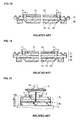
- An exemplary technique may be an opto-electric hybrid board as shown in FIG. 18 (for example, see Japanese Laid-open Patent Application Publication No. 2011-048150 ).
- the opto-electric hybrid board includes: a flexible circuit board E 0 including a flexible board 51 provided with an electrical interconnect line 52 on its front surface; and an optical waveguide (optical interconnection) W 0 (including an under cladding layer 56, a core 57 and an over cladding layer 58) made of epoxy resin or the like, the optical waveguide W 0 being stacked on the back surface (the surface opposite to the surface where the electrical interconnect line 52 is formed) of the flexible board 51.
- An optical element 4 is mounted on the flexible circuit board E 0 . Owing to the small thickness of both the flexible circuit board E 0 and the optical waveguide W 0 , the opto-electric hybrid board is flexible. Therefore, dealing with the recent trend toward miniaturization of the electronic devices and the like, the opto-electric hybrid board is suitable for use in a small space as being bent, or in a movable section such as a hinge.
- both the flexible circuit board E 0 and the optical waveguide W 0 deform under the pressure load caused by the mounting work. Accordingly, accurate mounting is difficult to be achieved, i.e., mounting workability is poor.
- another disclosed opto-electric hybrid board further includes, as shown in FIG. 19 , a stainless steel layer M 0 formed across the entire opto-electric hybrid board between the flexible circuit board E 0 and the optical waveguide W 0 (for example, see Japanese Laid-open Patent Application Publication No. 2009-265342 ).
- the opto-electric hybrid board exhibits excellent mounting workability with the optical element 4 since the stainless steel layer M 0 functions as reinforcement to suppress deformation under the pressure load caused by the mounting work with the optical element 4.
- the opto-electric hybrid board lacks flexibility. Therefore, the opto-electric hybrid board is not suitable for use in a small space as being bent, or for use in a movable section such as a hinge.
- an opto-electric hybrid board in which part of the over cladding layer of the optical waveguide is increased in thickness.
- the part corresponds to the mounting position of the optical element 4 where flexibility is not required (for example, see Japanese Laid-open Patent Application Publication Nos. 2010-286674 and 2011-017993 ).
- numerous dummy cores not used for optical communication are formed in the region on the front surface of the under cladding layer, which region corresponds to the part of the over cladding layer to be increased in thickness.
- the part of the over cladding layer covering the dummy core region becomes thick. This thickness suppresses deformation under the pressure load caused by the mounting work of the optical element 4, thereby improving mounting workability with the optical element.
- such practice invites the following problem in manufacturing.
- an element such as the optical element 4 is mounted on the opto-electric hybrid board by the ultrasonic mounting process.
- the ultrasonic mounting process is performed as follows. In a state where the opto-electric hybrid board is placed on a stage S with the optical waveguide W 0 being on the bottom side as shown in FIG. 20 , the optical element 4 attached to the tip of a nozzle N is pressed from above against electrodes 52a formed at the front surface of the flexible circuit board E 0 which is on the top side, and vibrated at the ultrasonic frequency in the direction being parallel (see arrow X in FIG. 20 ) to the plane being perpendicular to the pressing direction (see arrow Z in FIG. 20 ).
- the electrodes 52a of the flexible circuit board E 0 and gold bumps (not shown) formed on the surface of electrodes 4a of the optical element 4 are rubbed against each other, such that the electrodes 52a of the flexible circuit board E 0 and the gold bumps of the optical element 4 are fused by the frictional heat to be joined to each other.
- An opto-electric hybrid board which exhibits excellent flexibility as well as mounting workability with an element such as an optical element by the ultrasonic mounting process, and a method of manufacturing the same.
- a first aspect of an opto-electric hybrid board including:
- a second aspect provides a method of manufacturing an opto-electric hybrid board, including:
- the temperature of the opto-electric hybrid board when the element is being mounted refers to the temperature of the stage where the laminate made up of the electric circuit board, the metal layer and the optical waveguide (i.e., the opto-electric hybrid board excluding the element) is placed when the element is being mounted. Since the laminate is closely attached to the stage when the element is being mounted, the entire laminate achieves the temperature identical to that of the stage.
- the opto-electric hybrid board exhibits excellent flexibility, because the metal-made reinforcing layer and the resin-made reinforcing layer are formed not across the entire opto-electric hybrid board but at the portion corresponding to each element mounting electrode. Thus, the opto-electric hybrid board can be deformed, whereby versatility of the opto-electric hybrid board is enhanced. Further, since the metal-made reinforcing layer is formed between the electric circuit board and the optical waveguide, deformation under the pressure load caused by the mounting work of an element such as an optical element on the element mounting electrodes is suppressed.
- the resin-made reinforcing layer is provided at the core formed surface of the cladding layer, and the resin-made reinforcing layer is set to be greater than the cladding layer in the storage modulus at the temperature of the opto-electric hybrid board when the element is being mounted. Accordingly, when the element is being mounted on the element mounting electrodes by the ultrasonic mounting process, any deformation of the optical waveguide that may be caused by ultrasonic vibrations is suppressed. Thus, the element mounting electrodes and the electrodes of the element can be fully rubbed against each other, whereby full frictional heat can be generated. As a result, both of the electrodes are properly fused, whereby they are properly joined to each other. That is, the opto-electric hybrid board also exhibits excellent element mounting workability in the ultrasonic mounting process, owing to the synergetic effect of the metal-made reinforcing layer and the resin-made reinforcing layer.
- the core and the resin-made reinforcing layer are made of an identical photosensitive resin
- the core and the resin-made reinforcing layer are formed on an identical surface of the cladding layer. Accordingly, the core and the resin-made reinforcing layer can be formed at the same time, whereby excellent productivity is exhibited.
- the metal layer other than such a portion is removed by etching.
- the resin-made reinforcing layer is formed at a portion corresponding to each element mounting electrode in the cladding layer.
- the resin-made reinforcing layer is greater than the cladding layer in storage modulus at the temperature of the opto-electric hybrid board when the element is being mounted. Accordingly, the opto-electric hybrid board as described above, i.e., being excellent both in flexibility and in the element mounting workability in the ultrasonic mounting process, can be obtained.
- the resin-made reinforcing layer is made of a photosensitive resin layer formed on the cladding layer, and the resin-made reinforcing layer is formed simultaneously with the core by the photolithographic process, high productivity is achieved owing to such simultaneous production.
- FIG. 1A is a longitudinal sectional view schematically showing an opto-electric hybrid board according to a first preferred embodiment.
- FIG. 1B is a plan view of the opto-electric hybrid board.
- FIG. 1C is an enlarged view of a cross section (a section taken along line A-A in FIG. 1A ) of a portion corresponding to element mounting electrodes 2a. Note that, FIG. 1B only partially shows the structures such as the element mounting electrodes 2a, a metal-made reinforcing layer M, a resin-made reinforcing layer R, and a core 7 and the like, in order to clarify the arrangement of the element mounting electrodes 2a, the metal-made reinforcing layer M and the resin-made reinforcing layer R of the opto-electric hybrid board.
- the opto-electric hybrid board according to the present embodiment is strip-shaped as a whole, and includes : an electric circuit board E including a translucent insulative layer 1 and an electrical interconnect line 2 provided with element mounting electrodes 2a, the electrical interconnect line 2 being formed on the front surface of the insulative layer 1; an optical element 4 being in contact with the element mounting electrodes 2a of the electric circuit board E, the optical element 4 being bonded to the element mounting electrodes 2a using contact frictional heat generated between the optical element 4 and the element mounting electrodes 2a; and an optical waveguide W having its first cladding layer (under cladding layer) 6 formed so as to be in contact with the back surface of the insulative layer 1 of the electric circuit board E.
- a metal-made reinforcing layer M is provided at each of opposite longitudinal end portions, which correspond to the element mounting electrodes 2a.
- the opposite longitudinal end portions corresponding to the element mounting electrodes 2a are each provided with a resin-made reinforcing layer R.
- the resin-made reinforcing layer R is set to be greater than the first cladding layer 6 in the storage modulus at the temperature of the opto-electric hybrid board when the element is being mounted.
- the core 7 is made of the material identical to that of the resin-made reinforcing layer R.
- each longitudinal end portions of the strip-shaped opto-electric hybrid board four element mounting electrodes 2a are arranged at the four corners of a virtual rectangle.
- the center of the virtual rectangle serves as an optical path 5 between the optical element 4 mounted on the element mounting electrodes 2a and a reflecting surface (45 degree-inclined surface) 7a of the core 7.
- the metal-made reinforcing layer M is formed at each of the opposite longitudinal end portions of the opto-electric hybrid board so as to exclude the optical path 5 (i.e., so as to surround the optical path 5). Further, the metal-made reinforcing layer M is in contact with a grounding electrode 2b of the electrical interconnect line 2.
- one core 7 is formed from one end to the other end extending in the longitudinal direction and at the center in the width direction of the band-shaped opto-electric hybrid board.
- the resin-made reinforcing layer R is formed at each of the opposite sides of the core 7 with an interval from the core 7 near the element mounting electrodes 2a, and at each of the opposite longitudinal end portions of the opto-electric hybrid board.
- the metal-made reinforcing layer M and the resin-made reinforcing layer R are not formed across the entire opto-electric hybrid board, but only at the portions corresponding to the element mounting electrodes 2a in a limited manner. Accordingly, with the majority of the opto-electric hybrid board with no metal-made reinforcing layer M and resin-made reinforcing layer R, excellent flexibility is exhibited and a reduction in weight can be achieved.
- the opto-electric hybrid board can be reduced in thickness. Furthermore, the electric circuit board E and the optical waveguide W can be prevented from being deformed under the pressure load occurring when the optical element 4 is being mounted on the element mounting electrodes 2a. Thus, excellent mounting workability with the optical element 4 is exhibited.
- the optical waveguide can be prevented from being deformed by ultrasonic vibrations when the optical element 4 is being mounted on the element mounting electrodes 2a by the ultrasonic mounting process. Accordingly, the element mounting electrodes 2a and electrodes 4a of the optical element 4 can be fully rubbed against each other, whereby full frictional heat can be generated. As a result, the electrodes 2a and 4a can be properly fused, to be properly joined to each other.
- the metal-made reinforcing layer M is formed to surround the optical path 5, it functions to prevent the moisture, which degrades light propagation efficiency, from infiltrating from the side of the first cladding layer 6 into the optical path 5. That is, with the opto-electric hybrid board, flexibility and a reduction both in weight and thickness are achieved. Furthermore, simultaneously, the light propagation efficiency is prevented from being degraded by the moisture infiltrating into the optical path 5.
- the electric circuit board E includes the translucent insulative layer 1 and the electrical interconnect line 2 formed on the front surface of the insulative layer 1, as described above. Further, at the opposite longitudinal end portions of the opto-electric hybrid board, the element mounting electrodes 2a are formed as being uncovered on the front surface of the insulative layer 1, and the grounding electrode 2b is formed as being uncovered, penetrating through the insulative layer 1 to be brought into contact with the metal-made reinforcing layer M on the back surface of the insulative layer 1. The element mounting electrodes 2a and the grounding electrode 2b are part of the electrical interconnect line 2. The remainder of the electrical interconnect line 2 is covered by a coverlay 3, and is insulated and protected.
- the metal-made reinforcing layer M is formed at the portion at each end portion of the opto-electric hybrid board between the insulative layer 1 and the first cladding layer 6, so as to correspond to the four element mounting electrodes 2a.
- the thickness of the metal-made reinforcing layer M is set to fall within the range of 10 ⁇ m to 30 ⁇ m.
- the thickness of the metal-made reinforcing layer M being less than 10 ⁇ m can achieve a further reduction in thickness, it tends to be difficult to suppress the deformation associated with the mounting work of the optical element 4. Hence, a reduction in strength of the mounted product or in the positional precision of the optical element 4 may occur. Conversely, though the thickness of the metal-made reinforcing layer M being greater than 30 ⁇ m can fully suppress the deformation, since the first cladding layer 6 is formed to cover the metal-made reinforcing layer M, the first cladding layer 6 becomes thick. Hence, a reduction in flexibility of the opto-electric hybrid board may occur.
- the optical waveguide W includes, the first cladding layer (under cladding layer) 6, the core 7 and the resin-made reinforcing layer R formed on the front surface of the first cladding layer 6 in a predetermined pattern, and a second cladding layer (over cladding layer) 8 formed on the front surface of the first cladding layer 6 so as to cover the core 7 and the resin-made reinforcing layer R.
- the first cladding layer 6 is formed to cover the metal-made reinforcing layer M and to infill and bury the optical path 5.
- the back surface (the surface opposite to the surface where the core 7 is formed) of the first cladding layer 6 is in contact with the insulative layer 1 of the electric circuit board E.
- the portion of the core 7 corresponding to the optical path 5 is formed to be an inclined surface of 45 degrees relative to the longitudinal direction of the core 7.
- the inclined surface serves as a reflecting surface 7a that allows a light beam to propagate between the optical element 4 mounted on the element mounting electrodes 2a and the core 7. That is, at the reflecting surface 7a, the refractive index of the core 7 is greater than that of air outside the reflecting surface 7a. Therefore, when a light beam from a light-emitting element (optical element 4) or a light beam propagated through the core 7 impinges upon the reflecting surface 7a, a majority of the light beam is reflected to change the optical path thereof by 90 degrees.
- FIGS. 2A to 2D a method of manufacturing the opto-electric hybrid board will be described (see FIGS. 2A to 2D , FIGS. 3A to 3C , and FIGS. 4A and 4B ).
- a metal sheet member (metal layer) M 1 (see FIG. 2 A) for forming the metal-made reinforcing layer M is prepared.
- Exemplary metal materials for the metal sheet member M 1 (metal-made reinforcing layer M) include stainless steel, titanium, and various alloys.
- the thickness of the metal sheet member M 1 is set to fall within the range of 10 ⁇ m to 30 ⁇ m, similarly to the thickness of the metal-made reinforcing layer M.
- a photosensitive insulating resin including polyimide resin or the like is applied to the front surface of the metal sheet member M 1 , and the insulative layer 1 having a predetermined pattern is formed by the photolithographic process.
- a hole 1a for uncovering the portion of the front surface of the metal sheet member M 1 corresponding to the grounding electrode 2b is formed at each of the opposite longitudinal end portions. Note that the thickness of the insulative layer 1 is set to fall within the range of 3 ⁇ m to 30 ⁇ m.
- the electrical interconnect line (including the element mounting electrodes 2a and the grounding electrodes 2b) 2 is formed by a semi-additive process, for example.
- the semi-additive process is performed as follows. Firstly, a metal film (not shown) made of copper, chromium or the like is formed on the front surface of the insulative layer 1 by sputtering, electroless plating or the like. This metal film serves as a seed layer (a layer serving as a basis material for the formation of an electroplated layer) for the subsequent electroplating process.
- a photosensitive resist (not shown) is laminated onto each of the opposite surfaces of a laminate made up of the metal sheet member M 1 , the insulative layer 1 and the seed layer.
- the photolithographic process is performed to form a hole in the pattern of the electrical interconnect line 2 at the photosensitive resist on the side where the seed layer is formed, such that the surface portion of the seed layer is uncovered at the bottom of the hole.
- electroplating is performed to form an electroplated layer made of copper or the like in a stacked manner on the surface portion of the seed layer uncovered at the bottom of the hole.
- the photosensitive resist is stripped away using an aqueous sodium hydroxide solution or the like.
- the seed layer with no electroplated layer is removed by soft etching.
- the laminate portion made up of the remaining seed layer and the electroplated layer is the electrical interconnect line 2. Note that the thickness of the electrical interconnect line 2 is set to fall within the range of 5 ⁇ m to 35 ⁇ m.
- An electroless plated layer (not shown) made of nickel or the like is formed on the front surface of the electrical interconnect line (including the element mounting electrodes 2a and the grounding electrodes 2b) 2. Thereafter, as shown in FIG. 2C , a photosensitive insulating resin being polyimide resin or the like is applied to the electrical interconnect line 2 excluding the element mounting electrodes 2a and the grounding electrodes 2b, to form the coverlay 3 by the photolithographic process.
- the electroless plated layer (not shown) formed on the element mounting electrodes 2a and the grounding electrodes 2b is removed by etching. Thereafter, an electroplated layer (not shown) made of gold, nickel or the like is formed at each place where the electroless plated layer has been removed. In this manner, the electric circuit board E is formed on the front surface of the metal sheet member M 1 .
- a photosensitive resist (not shown) is laminated to each of the opposite faces of a laminate made up of the metal sheet member M 1 and the electric circuit board E. Thereafter, the photosensitive resist on the back surface side (the surface on the side opposite to the electric circuit board E) of the metal sheet member M 1 excluding the portion corresponding to the metal-made reinforcing layer M is removed by the photolithographic process, such that the back surface portion of the metal sheet member M 1 is uncovered at the bottom of the removed portion (the top side in the drawing).
- the portions of the metal sheet member M 1 uncovered at the removed portion are removed by etching using a suitable aqueous etching solution for the metal material of the metal sheet member M 1 (for example, an aqueous ferric chloride solution for a stainless steel layer), to form the metal-made reinforcing layer M, with the insulative layer 1 being uncovered at the bottom (the top side in the drawing) of the removed portions.
- a suitable aqueous etching solution for the metal material of the metal sheet member M 1 for example, an aqueous ferric chloride solution for a stainless steel layer
- the photosensitive resist is stripped away using an aqueous sodium hydroxide solution or the like.
- a photosensitive resin such as photosensitive epoxy resin being the material of the first cladding layer (under cladding layer) 6 is applied to the back surface of the insulative layer 1 so as to cover the metal-made reinforcing layer M. Thereafter, the applied layer is exposed to irradiation light. The applied layer thus heated cures, to form the first cladding layer 6.
- the thickness of the first cladding layer 6 (the thickness from the metal-made reinforcing layer M) is set to fall within the range of 3 ⁇ m to 30 ⁇ m.
- the back surface of the metal-made reinforcing layer M is on the top side when the optical waveguide W is being formed (i.e., when the above-described first cladding layer 6, the core 7 whose description will follow and the second cladding layer (over cladding layer) 8 whose description will follow are being formed).
- the core 7 and the resin-made reinforcing layer R of a predetermined pattern are simultaneously formed on the front surface (the bottom side in the drawing) of the first cladding layer 6 by the photolithographic process.
- the thickness of the core 7 and the resin-made reinforcing layer R is set to fall within the range of 20 ⁇ m to 100 ⁇ m.
- the width of the core 7 is set to fall within the range of 20 ⁇ m to 100 ⁇ m.
- the clearance between the core 7 and the resin-made reinforcing layer R are set to fall within the range of 5 ⁇ m to 100 ⁇ m.
- An exemplary material for the core 7 and the resin-made reinforcing layer R is a photosensitive resin similar to that for the first cladding layer 6.
- the core 7 and the resin-made reinforcing layer R become greater than the first cladding layer 6 in the storage modulus at the temperature of the opto-electric hybrid board when the element is being mounted.
- the refractive index and the storage modulus can be adjusted by, for example, modifying the selection of the types of the materials of the first cladding layer 6, the core 7 and the second cladding layer 8 or the composition ratio thereof.
- the storage modulus of the core 7 and the resin-made reinforcing layer R is set to fall within the range of 0. 5 GPa to 2.0 GPa whether it is at the temperature of the opto-electric hybrid board when the element is being mounted or at the room temperature (25C°) in use, and that the storage modulus of the first and second cladding layers 6 and 8 is set to fall within the range of 0.3 GPa to 1.5 GPa.
- the second cladding layer 8 is formed on the front surface (the bottom side in the drawing) of the first cladding layer 6 by the photolithographic process so as to cover the core 7 and the resin-made reinforcing layer R.
- the thickness (the thickness from the core 7) of the second cladding layer 8 is set to fall within the range of 3 ⁇ m to 50 ⁇ m.
- An exemplary material of the second cladding layer 8 is a photosensitive resin similar to that of the first cladding layer 6.
- portions (opposite end portions) of the optical waveguide W corresponding to the optical path 5 are formed into inclined surfaces inclined by 45 degrees relative to the longitudinal direction of the core 7, by laser beam machining, cutting work through use of a rotary blade whose tool angle is 45 degrees, or the like.
- portions of the core 7 positioned at the inclined surfaces each function as the reflecting surface 7a.
- the optical waveguide W is formed on the back surface of the electric circuit board E.
- the illustration on the top side is a longitudinal sectional view with the illustration on the bottom side being a cross-sectional view taken along line C-C in the top side illustration
- a laminate made up of the electric circuit board, the metal layer and the optical waveguide is placed on a stage (not shown) of an ultrasonic mounting machine, and the optical element 4 is mounted on the element mounting electrodes 2a by the ultrasonic mounting process.
- the metal-made reinforcing layer M can prevent the electric circuit board E and the optical waveguide W from being deformed by the pressure load.
- the resin-made reinforcing layer R can prevent the optical waveguide W from being deformed by ultrasonic vibrations. Accordingly, the element mounting electrodes 2a and the electrodes 4a of the optical element 4 can be fully rubbed against each other, whereby full frictional heat can be generated. As a result, the electrodes 2a and 4a can be properly fused and joined to each other. In this manner, the opto-electric hybrid board shown in FIGS. 1A to 1C is obtained.
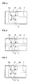
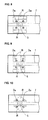
- FIGS. 5 to 10 are plan views schematically showing one end portions of opto-electric hybrid boards according to second to seventh preferred embodiments, respectively.
- FIGS. 5 to 10 correspond to the left part of FIG. 1B .
- FIGS. 5 to 10 only partially show the structures such as the element mounting electrodes 2a, the resin-made reinforcing layer R and the core 7 and the like, in order to clarify the arrangement of the element mounting electrodes 2a and the resin-made reinforcing layer R. Note that, since the metal-made reinforcing layer M is structured identically as shown in FIG. 1B , it is not illustrated.
- the metal-made reinforcing layer M according to each of the second to seventh preferred embodiments achieves functions and effects similar to those exhibited by the metal-made reinforcing layer M according to the first preferred embodiment.
- the core 7 is formed to extend just up to the portion corresponding to the optical path 5.
- the resin-made reinforcing layer R located on either side of the core 7 is formed to be continuous across that portion where the core 7 is not formed.
- the resin-made reinforcing layer R is formed.
- the core 7 is formed to extend just up to the portion corresponding to the optical path 5.
- the resin-made reinforcing layer R located on either side of the core 7 is formed to be continuous across that portion where the core 7 is not formed.
- the resin-made reinforcing layer R is formed as being divided into pieces aligned in the width direction of the opto-electric hybrid board.
- the resin-made reinforcing layer R is formed as being divided in the width direction and in the longitudinal direction of the opto-electric hybrid board.
- the resin-made reinforcing layer R is formed in a triangular shape that gradually narrows toward the side edge portion in the width direction of the opto-electric hybrid board.
- FIGS. 11 to 13 are plan views schematically showing one end portions of opto-electric hybrid boards according to the eighth to tenth preferred embodiments, respectively.
- the structure of each of the eighth to tenth preferred embodiments does not include the core 7 (see FIGS. 5 to 10 ) at the portion corresponding to the element mounting portion.
- FIGS. 11 to 13 only partially show the structures such as the element mounting electrodes 2a, the resin-made reinforcing layer R and the like, in order to clarify the arrangement of the element mounting electrodes 2a and the resin-made reinforcing layer R.
- the eighth to tenth preferred embodiments achieve functions and effects similar to those described in the first preferred embodiment.
- the resin-made reinforcing layer R is entirely and continuously formed across the portion corresponding to the element mounting portion.
- the resin-made reinforcing layer R is formed as being divided into pieces each elongated in the width direction of the opto-electric hybrid board.
- the resin-made reinforcing layer R is formed as being divided into pieces each elongated in the longitudinal direction of the opto-electric hybrid board.
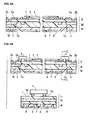
- FIGS. 14 to 17 are cross sectional views schematically showing one end portions of opto-electric hybrid boards according to eleventh to fourteenth preferred embodiments, respectively (corresponding to FIG. 1C ).
- the eleventh to fourteenth preferred embodiments achieve functions and effects similar to those described in the first preferred embodiment.
- the resin-made reinforcing layer R is formed to be thicker than the core 7. Accordingly, despite an increase in the thickness of the optical waveguide W, owing to a similar increase in the thickness of the resin-made reinforcing layer R, excellent mounting workability in the ultrasonic mounting process is exhibited. Note that, conversely, the resin-made reinforcing layer R may be formed to be thinner than the core 7 (not shown).
- the resin-made reinforcing layer R is structured at the layer being different from the core 7. Accordingly, despite an increase in the thickness of the optical waveguide W, owing to the resin-made reinforcing layer R, excellent mounting workability in the ultrasonic mounting process is exhibited.
- the first and second cladding layers 6 and 8 are not formed at the portion where the resin-made reinforcing layer R is formed. Accordingly, the thickness of the resin-made reinforcing layer R increases by the thickness of the first and second cladding layers 6 and 8, whereby excellent mounting workability in the ultrasonic mounting process is exhibited.
- the resin-made reinforcing layer R is formed at only one side in the width direction of the opto-electric hybrid board. Accordingly, though the mounting workability in the ultrasonic mounting process is inferior to the first preferred embodiment, it is at the sufficient level owing to the resin-made reinforcing layer R.
- the first and the eleventh to fourteenth preferred embodiments may be practiced in any combination.
- the ultrasonic wave in the ultrasonic mounting process oscillates linearly.
- the resin-made reinforcing layer R can be formed in various shapes as in the preferred embodiments described above, in order to secure tolerance for ultrasonic vibrations in mounting the element and an improvement in the mounting workability, it is preferable that the resin-made reinforcing layer R is formed as being elongated in the vibrating direction of the ultrasonic waves.
- the resin-made reinforcing layer R is made of the same material as that of the core 7 and the resin-made reinforcing layer R is simultaneously formed with the core 7. However, they may be made of different materials.
- the resin-made reinforcing layer R is set to be higher than the first cladding layer in the storage modulus at the temperature of the opto-electric hybrid board when the element is being mounted.
- the storage modulus of the resin-made reinforcing layer R at that temperature is set to be 0.5 GPa or more. The formation of the resin-made reinforcing layer R may precede that of the core 7, and vice versa.
- the optical element 4 is mounted on the element mounting electrodes 2a.
- the preferred embodiments can be similarly practiced when any element other than the optical element 4, such as an IC element, e.g., a VCSEL driver, a transimpedance amplifier or the like is to be mounted on the element mounting electrodes 2a.
- Electrodes 4a are present per element such as the optical element 4 in the preferred embodiments described above, more than four electrodes 4a may be present.
- one core 7 is present in the preferred embodiments described above, two or more cores may be formed.
- first and second cladding layers 6 and 8 are not patterned in the preferred embodiments described above, they may be patterned by the photolithographic process or the like.
- Example in conjunction with Comparative Example. Note that the present invention is not limited to Example.
- the opto-electric hybrid board according to the first preferred embodiment was employed as Example. Further, the length of the opto-electric hybrid board was set to 100 mm; the width of the opto-electric hybrid board was set to 7 mm; the thickness of the insulative layer was set to 5 ⁇ m; the thickness of the metal-made reinforcing layer was set to 20 ⁇ m; the thickness of the first cladding layer (the thickness from the metal-made reinforcing layer) was set to 20 ⁇ m; the thickness of the core was set to 50 ⁇ m; the width of the core was set to 50 ⁇ m; the thickness of the resin-made reinforcing layer was set to 50 ⁇ m; and the thickness of the second cladding layer (the thickness from the core) was set to 15 ⁇ m.
- the material of the first and second cladding layers was prepared by mixing modified aliphatic epoxy resin (EPICLON EXA-4816, available from DIC Corporation) by 50 parts by weight, bifunctional alicyclic epoxy resin (CELLOXIDE 2021P, available from Daicel Corporation) by 30 parts by weight, polycarbonatediol (PLACCEL CD205PL, available from Daicel Corporation) by 20 parts by weight, photoacid generator (SP170, available from ADEKA CORPORATION) 2 parts by weight, and ethyl lactate (available from Musashino Chemical Laboratory, Ltd.) 5 parts by weight.
- the storage modulus of the formed first second cladding layers was 1.2 GPa at 25C° and 0.7 GPa at the temperature of the opto-electric hybrid board when the element is being mounted (50C°).
- the material of the core and the resin-made reinforcing layer was prepared by mixing o-cresol novolac glycidyl ether (YDCN-700-10, available from NIPPON STEEL & SUMIKIN CHEMICAL CO., LTD.) by 50 parts by weight, bisphenoxy ethanol fluorene diglycidyl ether (OGSOL EG, available from Osaka Gas Chemicals Co., Ltd.) by 50 parts by weight, photoacid generator (SP170, available from ADEKA CORPORATION) by 1 part by weight, ethyl lactate (Musashino Chemical Laboratory, Ltd.) by 50 parts by weight.
- the storage modulus of the formed core and the resin-made reinforcing layer was 1.2 GPa at 25C° and 1.1 GPa at the temperature of the opto-electric hybrid board when the element is being bound (50C°).
- a light receiving element photodiode KPDG006HAl, available from Kyosemi Corporation
- FCB3 the ultrasonic mounting machine Flip Chip Bonder
- the mounting conditions were as follows: element temperature 150 C°; temperature of the opto-electric hybrid board 50C°; pressure load 1.0 N; ultrasonic wave output 3.0 W; and mounting time 0.5 seconds.
- the die shear strength was measured using a shear strength measuring device Bump Pull Tester (DAGE SERIES 5000, available from Dage Japan Co., Ltd.). As a result, while Example showed 1.1 N, Comparative Example showed 0.8 N.
- the opto-electric hybrid board and the method of manufacturing the same of the present invention are useful for mounting an optical element by the ultrasonic mounting process.
Landscapes
- Engineering & Computer Science (AREA)
- Microelectronics & Electronic Packaging (AREA)
- Physics & Mathematics (AREA)
- General Physics & Mathematics (AREA)
- Optics & Photonics (AREA)
- Optical Integrated Circuits (AREA)
- Optical Couplings Of Light Guides (AREA)
- Structure Of Printed Boards (AREA)
- Led Device Packages (AREA)
- Light Receiving Elements (AREA)
Abstract


Description
- The present invention relates to an opto-electric hybrid board being a laminate made up of an electric circuit board having an element such as an optical element mounted and an optical waveguide, and to a method of manufacturing the same.
- In recent electronic devices and the like, optical interconnection in addition to electrical interconnection has been used so as to address an increase in the amount of transmission information. An exemplary technique may be an opto-electric hybrid board as shown in
FIG. 18 (for example, see Japanese Laid-open Patent Application Publication No.2011-048150 flexible board 51 provided with anelectrical interconnect line 52 on its front surface; and an optical waveguide (optical interconnection) W0 (including an undercladding layer 56, acore 57 and an over cladding layer 58) made of epoxy resin or the like, the optical waveguide W0 being stacked on the back surface (the surface opposite to the surface where theelectrical interconnect line 52 is formed) of theflexible board 51. Anoptical element 4 is mounted on the flexible circuit board E0. Owing to the small thickness of both the flexible circuit board E0 and the optical waveguide W0, the opto-electric hybrid board is flexible. Therefore, dealing with the recent trend toward miniaturization of the electronic devices and the like, the opto-electric hybrid board is suitable for use in a small space as being bent, or in a movable section such as a hinge. - However, because of the flexibility, when the
optical element 4 is mounted on the flexible circuit board E0, both the flexible circuit board E0 and the optical waveguide W0 deform under the pressure load caused by the mounting work. Accordingly, accurate mounting is difficult to be achieved, i.e., mounting workability is poor. - On the other hand, another disclosed opto-electric hybrid board further includes, as shown in
FIG. 19 , a stainless steel layer M0 formed across the entire opto-electric hybrid board between the flexible circuit board E0 and the optical waveguide W0 (for example, see Japanese Laid-open Patent Application Publication No.2009-265342 optical element 4 since the stainless steel layer M0 functions as reinforcement to suppress deformation under the pressure load caused by the mounting work with theoptical element 4. - However, since the stainless steel layer M0 is provided across the entire opto-electric hybrid board, the opto-electric hybrid board lacks flexibility. Therefore, the opto-electric hybrid board is not suitable for use in a small space as being bent, or for use in a movable section such as a hinge.
- Accordingly, what is also disclosed is an opto-electric hybrid board in which part of the over cladding layer of the optical waveguide is increased in thickness. The part corresponds to the mounting position of the
optical element 4 where flexibility is not required (for example, see Japanese Laid-open Patent Application Publication Nos.2010-286674 2011-017993 optical element 4, thereby improving mounting workability with the optical element. However, such practice invites the following problem in manufacturing. - Generally, an element such as the
optical element 4 is mounted on the opto-electric hybrid board by the ultrasonic mounting process. The ultrasonic mounting process is performed as follows. In a state where the opto-electric hybrid board is placed on a stage S with the optical waveguide W0 being on the bottom side as shown inFIG. 20 , theoptical element 4 attached to the tip of a nozzle N is pressed from above againstelectrodes 52a formed at the front surface of the flexible circuit board E0 which is on the top side, and vibrated at the ultrasonic frequency in the direction being parallel (see arrow X inFIG. 20 ) to the plane being perpendicular to the pressing direction (see arrow Z inFIG. 20 ). Thus, theelectrodes 52a of the flexible circuit board E0 and gold bumps (not shown) formed on the surface ofelectrodes 4a of theoptical element 4 are rubbed against each other, such that theelectrodes 52a of the flexible circuit board E0 and the gold bumps of theoptical element 4 are fused by the frictional heat to be joined to each other. - However, though both the conventional opto-electric hybrid boards, i.e., the one including the stainless steel layer M0 between the flexible circuit board E0 and the optical waveguide W0 (Japanese Laid-open Patent Application Publication No.
2009-265342 optical element 4 is mounted (Japanese Laid-open Patent Application Publication Nos.2010-286674 2011-017993 optical element 4, the optical waveguide W0 being in contact with the stage vibrates in accordance with the ultrasonic vibrations and hence deforms (see the dashed-two dotted line inFIG. 20 ). Thus, friction between theelectrodes 52a of the flexible circuit board E0 and the gold bumps of theoptical element 4 becomes insufficient to generate full frictional heat, making it difficult for theelectrodes 52a of the flexible circuit board E0 and the gold bumps of theoptical element 4 to join to each other. In particular, since those with a great thickness (Japanese Laid-open Patent Application Publication Nos.2010-286674 2011-017993 - An opto-electric hybrid board is provided which exhibits excellent flexibility as well as mounting workability with an element such as an optical element by the ultrasonic mounting process, and a method of manufacturing the same.
- A first aspect of an opto-electric hybrid board, including:
- an electric circuit board including an insulative layer having front and back surfaces, and an element mounting electrode formed at a predetermined position on the front surface of the insulative layer;
- an element being in contact with the element mounting electrode, the element being mounted through use of contact frictional heat generated by being in contact with the element mounting electrode;
- an optical waveguide including a cladding layer and a core patterned on of the cladding layer, the electric circuit board and the optical waveguide being stacked together in a state where the cladding layer is in contact with the back surface of the insulative layer;
- a metal-made reinforcing layer formed between the insulative layer and the cladding layer at a portion corresponding to the element mounting electrode; and
- a resin-made reinforcing layer formed at a portion corresponding to the element mounting electrode, in the cladding layer where the core is formed, wherein
- the resin-made reinforcing layer is greater than the cladding layer in storage modulus at a temperature of the opto-electric hybrid board when the element is being mounted.
- Further, a second aspect provides a method of manufacturing an opto-electric hybrid board, including:
- forming an insulative layer on a front surface of a metal layer, thereafter forming an element mounting electrode on a front surface of the insulative layer, thereby forming an electric circuit board on the front surface of the metal layer;
- forming a cladding layer on a back surface of the metal layer, thereafter forming a core on the cladding layer, thereby forming an optical waveguide on the back surface of the metal layer; and
- bringing an element into frictional contact with the element mounting electrode to generate frictional heat, the element being mounted on the element mounting electrode through use of the frictional heat, the method further comprising, prior to the forming of the cladding layer:
- in order to leave a portion of the metal layer corresponding to the element mounting electrode, removing the metal layer other than the portion by etching, thereby forming the left portion into a metal-made reinforcing layer;
- forming the cladding layer at a portion where the metal layer is removed, with the metal-made reinforcing layer being covered; and
- forming a resin-made reinforcing layer at a portion corresponding to the element mounting electrode in the cladding layer, wherein
- the resin-made reinforcing layer is greater than the cladding layer in storage modulus at a temperature of the opto-electric hybrid board when the element is being mounted.
- Note that, "the temperature of the opto-electric hybrid board when the element is being mounted" refers to the temperature of the stage where the laminate made up of the electric circuit board, the metal layer and the optical waveguide (i.e., the opto-electric hybrid board excluding the element) is placed when the element is being mounted. Since the laminate is closely attached to the stage when the element is being mounted, the entire laminate achieves the temperature identical to that of the stage.
- The opto-electric hybrid board exhibits excellent flexibility, because the metal-made reinforcing layer and the resin-made reinforcing layer are formed not across the entire opto-electric hybrid board but at the portion corresponding to each element mounting electrode. Thus, the opto-electric hybrid board can be deformed, whereby versatility of the opto-electric hybrid board is enhanced. Further, since the metal-made reinforcing layer is formed between the electric circuit board and the optical waveguide, deformation under the pressure load caused by the mounting work of an element such as an optical element on the element mounting electrodes is suppressed. Furthermore, the resin-made reinforcing layer is provided at the core formed surface of the cladding layer, and the resin-made reinforcing layer is set to be greater than the cladding layer in the storage modulus at the temperature of the opto-electric hybrid board when the element is being mounted. Accordingly, when the element is being mounted on the element mounting electrodes by the ultrasonic mounting process, any deformation of the optical waveguide that may be caused by ultrasonic vibrations is suppressed. Thus, the element mounting electrodes and the electrodes of the element can be fully rubbed against each other, whereby full frictional heat can be generated. As a result, both of the electrodes are properly fused, whereby they are properly joined to each other. That is, the opto-electric hybrid board also exhibits excellent element mounting workability in the ultrasonic mounting process, owing to the synergetic effect of the metal-made reinforcing layer and the resin-made reinforcing layer.
- In particular, when the core and the resin-made reinforcing layer are made of an identical photosensitive resin, the core and the resin-made reinforcing layer are formed on an identical surface of the cladding layer. Accordingly, the core and the resin-made reinforcing layer can be formed at the same time, whereby excellent productivity is exhibited.
- In the method of manufacturing the opto-electric hybrid board, prior to forming the cladding layer, in order to leave a portion of the metal layer corresponding to each element mounting electrode, the metal layer other than such a portion is removed by etching. Further, the resin-made reinforcing layer is formed at a portion corresponding to each element mounting electrode in the cladding layer. The resin-made reinforcing layer is greater than the cladding layer in storage modulus at the temperature of the opto-electric hybrid board when the element is being mounted. Accordingly, the opto-electric hybrid board as described above, i.e., being excellent both in flexibility and in the element mounting workability in the ultrasonic mounting process, can be obtained.
- In particular, when the resin-made reinforcing layer is made of a photosensitive resin layer formed on the cladding layer, and the resin-made reinforcing layer is formed simultaneously with the core by the photolithographic process, high productivity is achieved owing to such simultaneous production.
-
-
FIG. 1A is a longitudinal sectional view schematically showing an opto-electric hybrid board according to a first preferred embodiment; -
FIG. 1B is a plan view schematically showing the opto-electric hybrid board; -
FIG. 1C is an enlarged view schematically showing a cross section taken along line A-A inFIG. 1A ; -
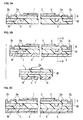
FIGS. 2A to 2D are illustrations schematically showing the steps of producing an electric circuit board and producing a metal-made reinforcing layer in a method of manufacturing the opto-electric hybrid board; -
FIGS. 3A to 3C are illustrations schematically showing the steps of producing an optical waveguide in the method of manufacturing the opto-electric hybrid board; -
FIG. 4A is an illustration schematically showing a step of producing the optical waveguide followingFIGS. 3A to 3C ; -
FIG. 4B is an illustration schematically showing a step of mounting an optical element in the method of manufacturing the opto-electric hybrid board; -
FIG. 5 is a plan view schematically showing an opto-electric hybrid board according to a second preferred embodiment; -
FIG. 6 is a plan view schematically showing an opto-electric hybrid board according to a third preferred embodiment; -
FIG. 7 is a plan view schematically showing an opto-electric hybrid board according to a fourth preferred embodiment; -
FIG. 8 is a plan view schematically showing an opto-electric hybrid board according to a fifth preferred embodiment; -
FIG. 9 is a plan view schematically showing an opto-electric hybrid board according to a sixth preferred embodiment; -
FIG. 10 is a plan view schematically showing an opto-electric hybrid board according to a seventh preferred embodiment; -
FIG. 11 is a plan view schematically showing an opto-electric hybrid board according to an eighth preferred embodiment; -
FIG. 12 is a plan view schematically showing an opto-electric hybrid board according to a ninth preferred embodiment; -
FIG. 13 is a plan view schematically showing an opto-electric hybrid board according to a tenth preferred embodiment; -
FIG. 14 is a cross sectional view schematically showing an opto-electric hybrid board according to an eleventh preferred embodiment; -
FIG. 15 is a cross sectional view schematically showing an opto-electric hybrid board according to a twelfth preferred embodiment; -
FIG. 16 is a cross sectional view schematically showing an opto-electric hybrid board according to a thirteenth preferred embodiment; -
FIG. 17 is a cross sectional view schematically showing an opto-electric hybrid board according to a fourteenth preferred embodiment; -
FIG. 18 is a longitudinal sectional view schematically showing a conventional opto-electric hybrid board; -
FIG. 19 is a longitudinal sectional view schematically showing another conventional opto-electric hybrid board; and -
FIG. 20 is an illustration schematically showing a step of mounting an optical element in a manufacturing method of the conventional opto-electric hybrid board. - Preferred embodiments of the present invention will now be described in detail with reference to the drawings.
-
FIG. 1A is a longitudinal sectional view schematically showing an opto-electric hybrid board according to a first preferred embodiment.FIG. 1B is a plan view of the opto-electric hybrid board.FIG. 1C is an enlarged view of a cross section (a section taken along line A-A inFIG. 1A ) of a portion corresponding toelement mounting electrodes 2a. Note that,FIG. 1B only partially shows the structures such as theelement mounting electrodes 2a, a metal-made reinforcing layer M, a resin-made reinforcing layer R, and acore 7 and the like, in order to clarify the arrangement of theelement mounting electrodes 2a, the metal-made reinforcing layer M and the resin-made reinforcing layer R of the opto-electric hybrid board. The opto-electric hybrid board according to the present embodiment is strip-shaped as a whole, and includes : an electric circuit board E including atranslucent insulative layer 1 and anelectrical interconnect line 2 provided withelement mounting electrodes 2a, theelectrical interconnect line 2 being formed on the front surface of theinsulative layer 1; anoptical element 4 being in contact with theelement mounting electrodes 2a of the electric circuit board E, theoptical element 4 being bonded to theelement mounting electrodes 2a using contact frictional heat generated between theoptical element 4 and theelement mounting electrodes 2a; and an optical waveguide W having its first cladding layer (under cladding layer) 6 formed so as to be in contact with the back surface of theinsulative layer 1 of the electric circuit board E. Between theinsulative layer 1 and thefirst cladding layer 6, a metal-made reinforcing layer M is provided at each of opposite longitudinal end portions, which correspond to theelement mounting electrodes 2a. Further, in the surface of thefirst cladding layer 6 on the side opposite to the insulative layer 1 (i.e., the surface where thecore 7 is formed), the opposite longitudinal end portions corresponding to theelement mounting electrodes 2a are each provided with a resin-made reinforcing layer R. The resin-made reinforcing layer R is set to be greater than thefirst cladding layer 6 in the storage modulus at the temperature of the opto-electric hybrid board when the element is being mounted. Further, in the present preferred embodiment, thecore 7 is made of the material identical to that of the resin-made reinforcing layer R. - Note that, in the present preferred embodiment, at each longitudinal end portions of the strip-shaped opto-electric hybrid board, four
element mounting electrodes 2a are arranged at the four corners of a virtual rectangle. The center of the virtual rectangle serves as anoptical path 5 between theoptical element 4 mounted on theelement mounting electrodes 2a and a reflecting surface (45 degree-inclined surface) 7a of thecore 7. The metal-made reinforcing layer M is formed at each of the opposite longitudinal end portions of the opto-electric hybrid board so as to exclude the optical path 5 (i.e., so as to surround the optical path 5). Further, the metal-made reinforcing layer M is in contact with agrounding electrode 2b of theelectrical interconnect line 2. - Further, in the present preferred embodiment, one
core 7 is formed from one end to the other end extending in the longitudinal direction and at the center in the width direction of the band-shaped opto-electric hybrid board. The resin-made reinforcing layer R is formed at each of the opposite sides of thecore 7 with an interval from thecore 7 near theelement mounting electrodes 2a, and at each of the opposite longitudinal end portions of the opto-electric hybrid board. - The metal-made reinforcing layer M and the resin-made reinforcing layer R are not formed across the entire opto-electric hybrid board, but only at the portions corresponding to the
element mounting electrodes 2a in a limited manner. Accordingly, with the majority of the opto-electric hybrid board with no metal-made reinforcing layer M and resin-made reinforcing layer R, excellent flexibility is exhibited and a reduction in weight can be achieved. - Further, since the metal-made reinforcing layer M and the resin-made reinforcing layer R are provided at the portions corresponding to the
element mounting electrodes 2a, the opto-electric hybrid board can be reduced in thickness. Furthermore, the electric circuit board E and the optical waveguide W can be prevented from being deformed under the pressure load occurring when theoptical element 4 is being mounted on theelement mounting electrodes 2a. Thus, excellent mounting workability with theoptical element 4 is exhibited. - Furthermore, since the resin-made reinforcing layer R is formed on the core formed surface of the
first cladding layer 6, and the resin-made reinforcing layer R is set to be greater than thefirst cladding layer 6 in the storage modulus at the temperature of the opto-electric hybrid board when the element is being mounted, the optical waveguide can be prevented from being deformed by ultrasonic vibrations when theoptical element 4 is being mounted on theelement mounting electrodes 2a by the ultrasonic mounting process. Accordingly, theelement mounting electrodes 2a andelectrodes 4a of theoptical element 4 can be fully rubbed against each other, whereby full frictional heat can be generated. As a result, theelectrodes - Further, since the metal-made reinforcing layer M is formed to surround the
optical path 5, it functions to prevent the moisture, which degrades light propagation efficiency, from infiltrating from the side of thefirst cladding layer 6 into theoptical path 5. That is, with the opto-electric hybrid board, flexibility and a reduction both in weight and thickness are achieved. Furthermore, simultaneously, the light propagation efficiency is prevented from being degraded by the moisture infiltrating into theoptical path 5. - In more detail, the electric circuit board E includes the
translucent insulative layer 1 and theelectrical interconnect line 2 formed on the front surface of theinsulative layer 1, as described above. Further, at the opposite longitudinal end portions of the opto-electric hybrid board, theelement mounting electrodes 2a are formed as being uncovered on the front surface of theinsulative layer 1, and thegrounding electrode 2b is formed as being uncovered, penetrating through theinsulative layer 1 to be brought into contact with the metal-made reinforcing layer M on the back surface of theinsulative layer 1. Theelement mounting electrodes 2a and thegrounding electrode 2b are part of theelectrical interconnect line 2. The remainder of theelectrical interconnect line 2 is covered by acoverlay 3, and is insulated and protected. - As described above, the metal-made reinforcing layer M is formed at the portion at each end portion of the opto-electric hybrid board between the
insulative layer 1 and thefirst cladding layer 6, so as to correspond to the fourelement mounting electrodes 2a. For the purpose of reducing the thickness of the opto-electric hybrid board and suppressing deformation of the electric circuit board E and the optical waveguide W which may occur when theoptical element 4 is mounted on theelement mounting electrodes 2a, the thickness of the metal-made reinforcing layer M is set to fall within the range of 10 µm to 30 µm. Though the thickness of the metal-made reinforcing layer M being less than 10 µm can achieve a further reduction in thickness, it tends to be difficult to suppress the deformation associated with the mounting work of theoptical element 4. Hence, a reduction in strength of the mounted product or in the positional precision of theoptical element 4 may occur. Conversely, though the thickness of the metal-made reinforcing layer M being greater than 30 µm can fully suppress the deformation, since thefirst cladding layer 6 is formed to cover the metal-made reinforcing layer M, thefirst cladding layer 6 becomes thick. Hence, a reduction in flexibility of the opto-electric hybrid board may occur. - The optical waveguide W includes, the first cladding layer (under cladding layer) 6, the
core 7 and the resin-made reinforcing layer R formed on the front surface of thefirst cladding layer 6 in a predetermined pattern, and a second cladding layer (over cladding layer) 8 formed on the front surface of thefirst cladding layer 6 so as to cover thecore 7 and the resin-made reinforcing layer R. Thefirst cladding layer 6 is formed to cover the metal-made reinforcing layer M and to infill and bury theoptical path 5. The back surface (the surface opposite to the surface where thecore 7 is formed) of thefirst cladding layer 6 is in contact with theinsulative layer 1 of the electric circuit board E. Further, at each of the opposite longitudinal end portions, the portion of thecore 7 corresponding to theoptical path 5 is formed to be an inclined surface of 45 degrees relative to the longitudinal direction of thecore 7. The inclined surface serves as a reflectingsurface 7a that allows a light beam to propagate between theoptical element 4 mounted on theelement mounting electrodes 2a and thecore 7. That is, at the reflectingsurface 7a, the refractive index of thecore 7 is greater than that of air outside the reflectingsurface 7a. Therefore, when a light beam from a light-emitting element (optical element 4) or a light beam propagated through thecore 7 impinges upon the reflectingsurface 7a, a majority of the light beam is reflected to change the optical path thereof by 90 degrees. - Next, a method of manufacturing the opto-electric hybrid board will be described (see
FIGS. 2A to 2D ,FIGS. 3A to 3C , andFIGS. 4A and 4B ). - Firstly, a metal sheet member (metal layer) M1 (see
FIG. 2 A) for forming the metal-made reinforcing layer M is prepared. Exemplary metal materials for the metal sheet member M1 (metal-made reinforcing layer M) include stainless steel, titanium, and various alloys. Further, the thickness of the metal sheet member M1 is set to fall within the range of 10 µm to 30 µm, similarly to the thickness of the metal-made reinforcing layer M. - Next, as shown in
FIG. 2A , a photosensitive insulating resin including polyimide resin or the like is applied to the front surface of the metal sheet member M1, and theinsulative layer 1 having a predetermined pattern is formed by the photolithographic process. In the present preferred embodiment, for the purpose of forming thegrounding electrode 2b to be in contact with the metal-made reinforcing layer M (metal sheet member M1), a hole 1a for uncovering the portion of the front surface of the metal sheet member M1 corresponding to thegrounding electrode 2b is formed at each of the opposite longitudinal end portions. Note that the thickness of theinsulative layer 1 is set to fall within the range of 3 µm to 30 µm. - Next, as shown in
FIG. 2B , the electrical interconnect line (including theelement mounting electrodes 2a and thegrounding electrodes 2b) 2 is formed by a semi-additive process, for example. The semi-additive process is performed as follows. Firstly, a metal film (not shown) made of copper, chromium or the like is formed on the front surface of theinsulative layer 1 by sputtering, electroless plating or the like. This metal film serves as a seed layer (a layer serving as a basis material for the formation of an electroplated layer) for the subsequent electroplating process. Then, a photosensitive resist (not shown) is laminated onto each of the opposite surfaces of a laminate made up of the metal sheet member M1, theinsulative layer 1 and the seed layer. Thereafter, the photolithographic process is performed to form a hole in the pattern of theelectrical interconnect line 2 at the photosensitive resist on the side where the seed layer is formed, such that the surface portion of the seed layer is uncovered at the bottom of the hole. Next, electroplating is performed to form an electroplated layer made of copper or the like in a stacked manner on the surface portion of the seed layer uncovered at the bottom of the hole. Then, the photosensitive resist is stripped away using an aqueous sodium hydroxide solution or the like. Thereafter, the seed layer with no electroplated layer is removed by soft etching. The laminate portion made up of the remaining seed layer and the electroplated layer is theelectrical interconnect line 2. Note that the thickness of theelectrical interconnect line 2 is set to fall within the range of 5 µm to 35 µm. - An electroless plated layer (not shown) made of nickel or the like is formed on the front surface of the electrical interconnect line (including the
element mounting electrodes 2a and thegrounding electrodes 2b) 2. Thereafter, as shown inFIG. 2C , a photosensitive insulating resin being polyimide resin or the like is applied to theelectrical interconnect line 2 excluding theelement mounting electrodes 2a and thegrounding electrodes 2b, to form thecoverlay 3 by the photolithographic process. - Then, the electroless plated layer (not shown) formed on the
element mounting electrodes 2a and thegrounding electrodes 2b is removed by etching. Thereafter, an electroplated layer (not shown) made of gold, nickel or the like is formed at each place where the electroless plated layer has been removed. In this manner, the electric circuit board E is formed on the front surface of the metal sheet member M1. - Next, a photosensitive resist (not shown) is laminated to each of the opposite faces of a laminate made up of the metal sheet member M1 and the electric circuit board E. Thereafter, the photosensitive resist on the back surface side (the surface on the side opposite to the electric circuit board E) of the metal sheet member M1 excluding the portion corresponding to the metal-made reinforcing layer M is removed by the photolithographic process, such that the back surface portion of the metal sheet member M1 is uncovered at the bottom of the removed portion (the top side in the drawing).
- Then, as shown in
FIG. 2D (the drawing on the top side is a longitudinal sectional view with the drawing on the bottom side being a bottom view), the portions of the metal sheet member M1 uncovered at the removed portion are removed by etching using a suitable aqueous etching solution for the metal material of the metal sheet member M1 (for example, an aqueous ferric chloride solution for a stainless steel layer), to form the metal-made reinforcing layer M, with theinsulative layer 1 being uncovered at the bottom (the top side in the drawing) of the removed portions. Thereafter, the photosensitive resist is stripped away using an aqueous sodium hydroxide solution or the like. - In order to form the optical waveguide W (see
FIG. 4A ) on the back surface (the bottom side in the drawing) of the electric circuit board E, firstly, as shown inFIG. 3A , a photosensitive resin such as photosensitive epoxy resin being the material of the first cladding layer (under cladding layer) 6 is applied to the back surface of theinsulative layer 1 so as to cover the metal-made reinforcing layer M. Thereafter, the applied layer is exposed to irradiation light. The applied layer thus heated cures, to form thefirst cladding layer 6. The thickness of the first cladding layer 6 (the thickness from the metal-made reinforcing layer M) is set to fall within the range of 3 µm to 30 µm. Note that, the back surface of the metal-made reinforcing layer M is on the top side when the optical waveguide W is being formed (i.e., when the above-describedfirst cladding layer 6, thecore 7 whose description will follow and the second cladding layer (over cladding layer) 8 whose description will follow are being formed). - Then, as shown in
FIG. 3B (the illustration on the top side is a longitudinal sectional view with the illustration on the bottom side being a cross-sectional view taken along line B-B in the top side drawing), thecore 7 and the resin-made reinforcing layer R of a predetermined pattern are simultaneously formed on the front surface (the bottom side in the drawing) of thefirst cladding layer 6 by the photolithographic process. The thickness of thecore 7 and the resin-made reinforcing layer R is set to fall within the range of 20 µm to 100 µm. The width of thecore 7 is set to fall within the range of 20 µm to 100 µm. The clearance between thecore 7 and the resin-made reinforcing layer R are set to fall within the range of 5 µm to 100 µm. - An exemplary material for the
core 7 and the resin-made reinforcing layer R is a photosensitive resin similar to that for thefirst cladding layer 6. Here, what is used is the material that exhibits greater refractive index than the above-describedfirst cladding layer 6 and thesecond cladding layer 8, whose description will follow (seeFIG. 3C ), in the state where thecore 7 and the resin-made reinforcing layer R are formed. Further, with the material, thecore 7 and the resin-made reinforcing layer R become greater than thefirst cladding layer 6 in the storage modulus at the temperature of the opto-electric hybrid board when the element is being mounted. The refractive index and the storage modulus can be adjusted by, for example, modifying the selection of the types of the materials of thefirst cladding layer 6, thecore 7 and thesecond cladding layer 8 or the composition ratio thereof. - The higher storage modulus is better in view of element mounting workability, whereas the smaller storage modulus is better in view of flexibility in use. Accordingly, it is preferable that the storage modulus of the
core 7 and the resin-made reinforcing layer R is set to fall within the range of 0. 5 GPa to 2.0 GPa whether it is at the temperature of the opto-electric hybrid board when the element is being mounted or at the room temperature (25C°) in use, and that the storage modulus of the first and second cladding layers 6 and 8 is set to fall within the range of 0.3 GPa to 1.5 GPa. - Next, as shown in
FIG. 3C , thesecond cladding layer 8 is formed on the front surface (the bottom side in the drawing) of thefirst cladding layer 6 by the photolithographic process so as to cover thecore 7 and the resin-made reinforcing layer R. The thickness (the thickness from the core 7) of thesecond cladding layer 8 is set to fall within the range of 3 µm to 50 µm. An exemplary material of thesecond cladding layer 8 is a photosensitive resin similar to that of thefirst cladding layer 6. - Then, as shown in
FIG. 4A , portions (opposite end portions) of the optical waveguide W corresponding to the optical path 5 (positioned at a lower part in the drawing) are formed into inclined surfaces inclined by 45 degrees relative to the longitudinal direction of thecore 7, by laser beam machining, cutting work through use of a rotary blade whose tool angle is 45 degrees, or the like. Thus, such portions of thecore 7 positioned at the inclined surfaces each function as the reflectingsurface 7a. In this manner, the optical waveguide W is formed on the back surface of the electric circuit board E. - Thereafter, as shown in
FIG. 4B (the illustration on the top side is a longitudinal sectional view with the illustration on the bottom side being a cross-sectional view taken along line C-C in the top side illustration), a laminate made up of the electric circuit board, the metal layer and the optical waveguide is placed on a stage (not shown) of an ultrasonic mounting machine, and theoptical element 4 is mounted on theelement mounting electrodes 2a by the ultrasonic mounting process. At this time, though a pressure load is applied to the electric circuit board E and the optical waveguide W, the metal-made reinforcing layer M can prevent the electric circuit board E and the optical waveguide W from being deformed by the pressure load. Further, though ultrasonic vibrations are applied to the optical waveguide W, the resin-made reinforcing layer R can prevent the optical waveguide W from being deformed by ultrasonic vibrations. Accordingly, theelement mounting electrodes 2a and theelectrodes 4a of theoptical element 4 can be fully rubbed against each other, whereby full frictional heat can be generated. As a result, theelectrodes FIGS. 1A to 1C is obtained. -
FIGS. 5 to 10 are plan views schematically showing one end portions of opto-electric hybrid boards according to second to seventh preferred embodiments, respectively.FIGS. 5 to 10 correspond to the left part ofFIG. 1B .FIGS. 5 to 10 only partially show the structures such as theelement mounting electrodes 2a, the resin-made reinforcing layer R and thecore 7 and the like, in order to clarify the arrangement of theelement mounting electrodes 2a and the resin-made reinforcing layer R. Note that, since the metal-made reinforcing layer M is structured identically as shown inFIG. 1B , it is not illustrated. The metal-made reinforcing layer M according to each of the second to seventh preferred embodiments achieves functions and effects similar to those exhibited by the metal-made reinforcing layer M according to the first preferred embodiment. - In the second preferred embodiment shown in
FIG. 5 , in the structure of the first preferred embodiment shown inFIGS. 1A to 1C , thecore 7 is formed to extend just up to the portion corresponding to theoptical path 5. The resin-made reinforcing layer R located on either side of thecore 7 is formed to be continuous across that portion where thecore 7 is not formed. - In the third preferred embodiment shown in
FIG. 6 , in the first preferred embodiment shown inFIGS. 1A to 1C , for each portion corresponding to eachelement mounting electrode 2a, the resin-made reinforcing layer R is formed. - In the fourth preferred embodiment shown in
FIG. 7 , in the structure of the third preferred embodiment shown inFIG. 6 , thecore 7 is formed to extend just up to the portion corresponding to theoptical path 5. The resin-made reinforcing layer R located on either side of thecore 7 is formed to be continuous across that portion where thecore 7 is not formed. - In the fifth preferred embodiment shown in
FIG. 8 , in the structure of the first preferred embodiment shown inFIGS. 1A to 1C , the resin-made reinforcing layer R is formed as being divided into pieces aligned in the width direction of the opto-electric hybrid board. - In the second preferred embodiment shown in
FIG. 5 , in the structure of the first preferred embodiment shown inFIGS. 1A to 1C , the resin-made reinforcing layer R is formed as being divided in the width direction and in the longitudinal direction of the opto-electric hybrid board. - In the seventh preferred embodiment shown in
FIG. 10 , in the first preferred embodiment shown inFIGS. 1A to 1C , the resin-made reinforcing layer R is formed in a triangular shape that gradually narrows toward the side edge portion in the width direction of the opto-electric hybrid board. -
FIGS. 11 to 13 are plan views schematically showing one end portions of opto-electric hybrid boards according to the eighth to tenth preferred embodiments, respectively. The structure of each of the eighth to tenth preferred embodiments does not include the core 7 (seeFIGS. 5 to 10 ) at the portion corresponding to the element mounting portion.FIGS. 11 to 13 only partially show the structures such as theelement mounting electrodes 2a, the resin-made reinforcing layer R and the like, in order to clarify the arrangement of theelement mounting electrodes 2a and the resin-made reinforcing layer R. The eighth to tenth preferred embodiments achieve functions and effects similar to those described in the first preferred embodiment. - In the eighth preferred embodiment shown in
FIG. 11 , the resin-made reinforcing layer R is entirely and continuously formed across the portion corresponding to the element mounting portion. - In the ninth preferred embodiment shown in
FIG. 12 , in the structure of the eighth preferred embodiment shown inFIG. 11 , the resin-made reinforcing layer R is formed as being divided into pieces each elongated in the width direction of the opto-electric hybrid board. - In the tenth preferred embodiment shown in
FIG. 13 , in the structure of the eighth preferred embodiment shown inFIG. 11 , the resin-made reinforcing layer R is formed as being divided into pieces each elongated in the longitudinal direction of the opto-electric hybrid board. -
FIGS. 14 to 17 are cross sectional views schematically showing one end portions of opto-electric hybrid boards according to eleventh to fourteenth preferred embodiments, respectively (corresponding toFIG. 1C ). The eleventh to fourteenth preferred embodiments achieve functions and effects similar to those described in the first preferred embodiment. - In the eleventh preferred embodiment shown in
FIG. 14 , in the structure of the first preferred embodiment shown inFIGS. 1A to 1C , the resin-made reinforcing layer R is formed to be thicker than thecore 7. Accordingly, despite an increase in the thickness of the optical waveguide W, owing to a similar increase in the thickness of the resin-made reinforcing layer R, excellent mounting workability in the ultrasonic mounting process is exhibited. Note that, conversely, the resin-made reinforcing layer R may be formed to be thinner than the core 7 (not shown). - In the twelfth preferred embodiment shown in
FIG. 15 , in the structure of the first preferred embodiment shown inFIGS. 1A to 1C , the resin-made reinforcing layer R is structured at the layer being different from thecore 7. Accordingly, despite an increase in the thickness of the optical waveguide W, owing to the resin-made reinforcing layer R, excellent mounting workability in the ultrasonic mounting process is exhibited. - In the thirteenth preferred embodiment shown in
FIG. 16 , in the structure of the first preferred embodiment shown inFIGS. 1A to 1C , the first and second cladding layers 6 and 8 (seeFIG. 1C ) are not formed at the portion where the resin-made reinforcing layer R is formed. Accordingly, the thickness of the resin-made reinforcing layer R increases by the thickness of the first and second cladding layers 6 and 8, whereby excellent mounting workability in the ultrasonic mounting process is exhibited. - In the fourteenth preferred embodiment shown in
FIG. 17 , in the structure of the first preferred embodiment shown inFIGS. 1A to 1C , the resin-made reinforcing layer R is formed at only one side in the width direction of the opto-electric hybrid board. Accordingly, though the mounting workability in the ultrasonic mounting process is inferior to the first preferred embodiment, it is at the sufficient level owing to the resin-made reinforcing layer R. - The first and the eleventh to fourteenth preferred embodiments may be practiced in any combination.
- Here, the ultrasonic wave in the ultrasonic mounting process oscillates linearly. While the resin-made reinforcing layer R can be formed in various shapes as in the preferred embodiments described above, in order to secure tolerance for ultrasonic vibrations in mounting the element and an improvement in the mounting workability, it is preferable that the resin-made reinforcing layer R is formed as being elongated in the vibrating direction of the ultrasonic waves.
- In the preferred embodiments described above, the resin-made reinforcing layer R is made of the same material as that of the
core 7 and the resin-made reinforcing layer R is simultaneously formed with thecore 7. However, they may be made of different materials. In this case, the resin-made reinforcing layer R is set to be higher than the first cladding layer in the storage modulus at the temperature of the opto-electric hybrid board when the element is being mounted. Furthermore, the storage modulus of the resin-made reinforcing layer R at that temperature is set to be 0.5 GPa or more. The formation of the resin-made reinforcing layer R may precede that of thecore 7, and vice versa. - In the preferred embodiments described above, the
optical element 4 is mounted on theelement mounting electrodes 2a. However, the preferred embodiments can be similarly practiced when any element other than theoptical element 4, such as an IC element, e.g., a VCSEL driver, a transimpedance amplifier or the like is to be mounted on theelement mounting electrodes 2a. - Further, though four
electrodes 4a are present per element such as theoptical element 4 in the preferred embodiments described above, more than fourelectrodes 4a may be present. - Still further, though one
core 7 is present in the preferred embodiments described above, two or more cores may be formed. - Further, though the first and second cladding layers 6 and 8 are not patterned in the preferred embodiments described above, they may be patterned by the photolithographic process or the like.
- Next, a description will be given of Example in conjunction with Comparative Example. Note that the present invention is not limited to Example.
- The opto-electric hybrid board according to the first preferred embodiment was employed as Example. Further, the length of the opto-electric hybrid board was set to 100 mm; the width of the opto-electric hybrid board was set to 7 mm; the thickness of the insulative layer was set to 5 µm; the thickness of the metal-made reinforcing layer was set to 20 µm; the thickness of the first cladding layer (the thickness from the metal-made reinforcing layer) was set to 20 µm; the thickness of the core was set to 50 µm; the width of the core was set to 50 µm; the thickness of the resin-made reinforcing layer was set to 50 µm; and the thickness of the second cladding layer (the thickness from the core) was set to 15 µm.
- Here, the material of the first and second cladding layers was prepared by mixing modified aliphatic epoxy resin (EPICLON EXA-4816, available from DIC Corporation) by 50 parts by weight, bifunctional alicyclic epoxy resin (CELLOXIDE 2021P, available from Daicel Corporation) by 30 parts by weight, polycarbonatediol (PLACCEL CD205PL, available from Daicel Corporation) by 20 parts by weight, photoacid generator (SP170, available from ADEKA CORPORATION) 2 parts by weight, and ethyl lactate (available from Musashino Chemical Laboratory, Ltd.) 5 parts by weight. The storage modulus of the formed first second cladding layers was 1.2 GPa at 25C° and 0.7 GPa at the temperature of the opto-electric hybrid board when the element is being mounted (50C°).
- Further, the material of the core and the resin-made reinforcing layer was prepared by mixing o-cresol novolac glycidyl ether (YDCN-700-10, available from NIPPON STEEL & SUMIKIN CHEMICAL CO., LTD.) by 50 parts by weight, bisphenoxy ethanol fluorene diglycidyl ether (OGSOL EG, available from Osaka Gas Chemicals Co., Ltd.) by 50 parts by weight, photoacid generator (SP170, available from ADEKA CORPORATION) by 1 part by weight, ethyl lactate (Musashino Chemical Laboratory, Ltd.) by 50 parts by weight. The storage modulus of the formed core and the resin-made reinforcing layer was 1.2 GPa at 25C° and 1.1 GPa at the temperature of the opto-electric hybrid board when the element is being bound (50C°).
- An opto-electric hybrid board according to Example with no resin-made reinforcing layer was employed as Comparative Example.
- On the element mounting electrodes of each of the opto-electric hybrid board according to Example and according to Comparative Example, a light receiving element (photodiode KPDG006HAl, available from Kyosemi Corporation) was mounted using the ultrasonic mounting machine Flip Chip Bonder (FCB3, available from Panasonic Factory Solutions Co., Ltd.). The mounting conditions were as follows: element temperature 150 C°; temperature of the opto-electric hybrid board 50C°; pressure load 1.0 N; ultrasonic wave output 3.0 W; and mounting time 0.5 seconds. The die shear strength was measured using a shear strength measuring device Bump Pull Tester (DAGE SERIES 5000, available from Dage Japan Co., Ltd.). As a result, while Example showed 1.1 N, Comparative Example showed 0.8 N.
- From the results above, it can be seen that the element is strongly mounted by the ultrasonic mounting process on Example with the resin-made reinforcing layer, as compared to Comparative Example with no resin-made reinforcing layer.
- The opto-electric hybrid board and the method of manufacturing the same of the present invention are useful for mounting an optical element by the ultrasonic mounting process.
- Although specific forms of embodiments of the instant invention have been described above and illustrated in the accompanying drawings in order to be more clearly understood, the above description is made by way of example and not as a limitation to the scope of the instant invention. It is contemplated that various modifications apparent to one of ordinary skill in the art could be made without departing from the scope of the invention.
Claims (4)
- An opto-electric hybrid board, comprising:an electric circuit board including an insulative layer having front and back surfaces, and an element mounting electrode formed at a predetermined position on the front surface of the insulative layer;an element being in contact with the element mounting electrode, the element being mounted through use of contact frictional heat generated by being in contact with the element mounting electrode;an optical waveguide including a cladding layer and a core patterned on the cladding layer, the electric circuit board and the optical waveguide being stacked together in a state where the cladding layer is in contact with the back surface of the insulative layer;a metal-made reinforcing layer formed between the insulative layer and the cladding layer at a portion corresponding to the element mounting electrode; anda resin-made reinforcing layer formed at a portion corresponding to the element mounting electrode, in the cladding layer where the core is formed, whereinthe resin-made reinforcing layer is greater than the cladding layer in storage modulus at a temperature of the opto-electric hybrid board when the element is being mounted.
- The opto-electric hybrid board according to claim 1, wherein
the core and the resin-made reinforcing layer are made of an identical photosensitive resin. - A method of manufacturing an opto-electric hybrid board, comprising:forming an insulative layer on a front surface of a metal layer, thereafter forming an element mounting electrode on a front surface of the insulative layer, thereby forming an electric circuit board on the front surface of the metal layer;forming a cladding layer on a back surface of the metal layer, thereafter forming a core on the cladding layer, thereby forming an optical waveguide on the back surface of the metal layer; andbringing an element into frictional contact with the element mounting electrode to generate frictional heat, the element being mounted on the element mounting electrode through use of the frictional heat,wherein, for forming the optical waveguide, prior to the forming of the cladding layer, removing the metal layer other than a portion of the metal layer corresponding to the element mounting electrode by etching, thereby forming a remaining portion into a metal-made reinforcing layer;forming the cladding layer at the portion where the metal layer is removed, with the metal-made reinforcing layer being covered; andforming a resin-made reinforcing layer at a portion corresponding to the element mounting electrode in the cladding layer, whereinthe resin-made reinforcing layer is greater than the cladding layer in storage modulus at a temperature of the opto-electric hybrid board when the element is being mounted.
- The method of manufacturing an opto-electric hybrid board according to claim 3, further comprising
forming a photosensitive resin layer on the cladding layer, wherein
the resin-made reinforcing layer is formed simultaneously with the core through a photolithographic process from the photosensitive resin layer.
Applications Claiming Priority (1)
| Application Number | Priority Date | Filing Date | Title |
|---|---|---|---|
| JP2012259048A JP6202662B2 (en) | 2012-11-27 | 2012-11-27 | Opto-electric hybrid board and manufacturing method thereof |
Publications (1)
| Publication Number | Publication Date |
|---|---|
| EP2736309A1 true EP2736309A1 (en) | 2014-05-28 |
Family
ID=49447465
Family Applications (1)
| Application Number | Title | Priority Date | Filing Date |
|---|---|---|---|
| EP13189697.9A Withdrawn EP2736309A1 (en) | 2012-11-27 | 2013-10-22 | Opto-electric hybrid board and method of manufacturing same |
Country Status (6)
| Country | Link |
|---|---|
| US (1) | US9297958B2 (en) |
| EP (1) | EP2736309A1 (en) |
| JP (1) | JP6202662B2 (en) |
| KR (1) | KR102036928B1 (en) |
| CN (1) | CN103837932B (en) |
| TW (1) | TWI594029B (en) |
Cited By (1)
| Publication number | Priority date | Publication date | Assignee | Title |
|---|---|---|---|---|
| CN117055236A (en) * | 2023-10-11 | 2023-11-14 | 成都万应微电子有限公司 | Optical beam expansion system and photoelectric equipment |
Families Citing this family (22)
| Publication number | Priority date | Publication date | Assignee | Title |
|---|---|---|---|---|
| JP2014238491A (en) * | 2013-06-07 | 2014-12-18 | 日東電工株式会社 | Opto-electric hybrid module |
| JP6202566B2 (en) * | 2013-10-29 | 2017-09-27 | 日東電工株式会社 | Opto-electric hybrid board and manufacturing method thereof |
| JP6712742B2 (en) * | 2014-09-24 | 2020-06-24 | 日東電工株式会社 | Opto-electric hybrid board and its manufacturing method |
| WO2016047447A1 (en) * | 2014-09-24 | 2016-03-31 | 日東電工株式会社 | Opto-electric hybrid board and manufacturing method for same |
| JP6525240B2 (en) * | 2014-10-24 | 2019-06-05 | 日東電工株式会社 | Opto-electric hybrid board and its manufacturing method |
| JP6460515B2 (en) * | 2014-10-24 | 2019-01-30 | 日東電工株式会社 | Opto-electric hybrid board and manufacturing method thereof |
| JP6460516B2 (en) * | 2014-10-28 | 2019-01-30 | 日東電工株式会社 | Opto-electric hybrid board |
| JP6653857B2 (en) | 2014-11-25 | 2020-02-26 | 日東電工株式会社 | Opto-electric hybrid board and its manufacturing method |
| JP6674691B2 (en) * | 2014-12-10 | 2020-04-01 | 日東電工株式会社 | Opto-electric hybrid board |
| JPWO2017145289A1 (en) * | 2016-02-24 | 2018-12-13 | オリンパス株式会社 | Optical transmission module, endoscope, and manufacturing method of optical transmission module |
| JP6959731B2 (en) * | 2016-11-30 | 2021-11-05 | 日東電工株式会社 | Optical-electric mixed board |
| CN106783878A (en) * | 2016-12-19 | 2017-05-31 | 京东方科技集团股份有限公司 | Display base plate and preparation method thereof, display panel and crimping apparatus |
| JP7002886B2 (en) * | 2017-08-22 | 2022-01-20 | 日東電工株式会社 | Optical Waveguide, Opto-Electricity Consolidation Board, and Opto-Electricity Consolidation Module |
| JP7258486B2 (en) | 2018-07-25 | 2023-04-17 | 日東電工株式会社 | Optical waveguide member connector and manufacturing method thereof |
| JP7280031B2 (en) * | 2018-11-14 | 2023-05-23 | 新光電気工業株式会社 | Optical waveguide mounting substrate, optical communication device, and method for manufacturing optical waveguide mounting substrate |
| JP7353056B2 (en) | 2019-03-29 | 2023-09-29 | 日東電工株式会社 | Optical/electrical hybrid board with optical element |
| JP7372754B2 (en) * | 2019-03-29 | 2023-11-01 | 日東電工株式会社 | Optical/electrical hybrid board |
| JP2021028664A (en) * | 2019-08-09 | 2021-02-25 | 日東電工株式会社 | Photo-electric composite transmission module |
| CN110783326B (en) * | 2019-10-31 | 2021-12-17 | 京东方科技集团股份有限公司 | Substrate, preparation method thereof, display panel and display device |
| TWI884282B (en) * | 2020-06-22 | 2025-05-21 | 日商日東電工股份有限公司 | Optical communication module substrate |
| US12366715B2 (en) * | 2020-07-29 | 2025-07-22 | Nitto Denko Corporation | Opto-electric hybrid board |
| JP7852307B2 (en) * | 2022-03-11 | 2026-04-28 | 日本電気株式会社 | Waveguide substrate, optical module, and method for manufacturing the optical module |
Citations (6)
| Publication number | Priority date | Publication date | Assignee | Title |
|---|---|---|---|---|
| EP1967876A1 (en) * | 2005-12-27 | 2008-09-10 | Ibiden Co., Ltd. | Optical and electrical composite wiring board and method for fabricating same |
| EP2112534A1 (en) * | 2008-04-24 | 2009-10-28 | Nitto Denko Corporation | Manufacturing method of opto-electric hybrid board |
| WO2010110496A2 (en) * | 2009-03-26 | 2010-09-30 | Panasonic Electric Works Co., Ltd. | Method of manufacturing optical waveguide having mirror face, and optoelectronic composite wiring board |
| JP2010286674A (en) | 2009-06-11 | 2010-12-24 | Hitachi Chem Co Ltd | Optical waveguide and photoelectric composite wiring board |
| JP2011017993A (en) | 2009-07-10 | 2011-01-27 | Hitachi Chem Co Ltd | Optical waveguide and optoelectric compound wiring board |
| JP2011048150A (en) | 2009-08-27 | 2011-03-10 | Hitachi Chem Co Ltd | Method of manufacturing photoelectric flexible wiring board |
Family Cites Families (13)
| Publication number | Priority date | Publication date | Assignee | Title |
|---|---|---|---|---|
| JP3194397B2 (en) * | 1991-08-05 | 2001-07-30 | 日本電信電話株式会社 | Optical waveguide circuit module |
| JP2003050326A (en) * | 2001-08-07 | 2003-02-21 | Furukawa Electric Co Ltd:The | Optical waveguide components |
| JP2007033831A (en) * | 2005-07-26 | 2007-02-08 | Fuji Xerox Co Ltd | Flexible optical waveguide |
| JP4847389B2 (en) * | 2007-04-11 | 2011-12-28 | 日東電工株式会社 | Optical waveguide for touch panel and touch panel using the same |
| JP4971248B2 (en) * | 2008-05-27 | 2012-07-11 | 日東電工株式会社 | Manufacturing method of opto-electric hybrid module |
| JP5271141B2 (en) * | 2009-04-06 | 2013-08-21 | 日東電工株式会社 | Manufacturing method of opto-electric hybrid module and opto-electric hybrid module obtained thereby |
| JP2010266598A (en) * | 2009-05-13 | 2010-11-25 | Hitachi Cable Ltd | Optical wiring member |
| JP5467826B2 (en) * | 2009-09-16 | 2014-04-09 | 日東電工株式会社 | Opto-electric hybrid module and manufacturing method thereof |
| KR101067793B1 (en) * | 2009-11-13 | 2011-09-27 | 삼성전기주식회사 | Flexible Optical Substrate and Manufacturing Method Thereof |
| TW201222034A (en) * | 2010-04-06 | 2012-06-01 | Sumitomo Bakelite Co | An optical waveguide structure and an electronic device |
| JP2011249383A (en) * | 2010-05-24 | 2011-12-08 | Sumitomo Electric Printed Circuit Inc | Flexible printed-wiring board, connection structure, and electronic apparatus |
| JP2012042731A (en) * | 2010-08-19 | 2012-03-01 | Toshiba Corp | Flexible optical wiring board, and flexible optical wiring module |
| JP2012194401A (en) * | 2011-03-16 | 2012-10-11 | Nitto Denko Corp | Opto-electric hybrid substrate and manufacturing method of the same |
-
2012
- 2012-11-27 JP JP2012259048A patent/JP6202662B2/en not_active Expired - Fee Related
-
2013
- 2013-10-03 US US14/045,353 patent/US9297958B2/en active Active
- 2013-10-18 CN CN201310491908.2A patent/CN103837932B/en not_active Expired - Fee Related
- 2013-10-22 EP EP13189697.9A patent/EP2736309A1/en not_active Withdrawn
- 2013-10-23 TW TW102138237A patent/TWI594029B/en not_active IP Right Cessation
- 2013-10-24 KR KR1020130126961A patent/KR102036928B1/en not_active Expired - Fee Related
Patent Citations (7)
| Publication number | Priority date | Publication date | Assignee | Title |
|---|---|---|---|---|
| EP1967876A1 (en) * | 2005-12-27 | 2008-09-10 | Ibiden Co., Ltd. | Optical and electrical composite wiring board and method for fabricating same |
| EP2112534A1 (en) * | 2008-04-24 | 2009-10-28 | Nitto Denko Corporation | Manufacturing method of opto-electric hybrid board |
| JP2009265342A (en) | 2008-04-24 | 2009-11-12 | Nitto Denko Corp | Method for manufacturing opto-electric hybrid board |
| WO2010110496A2 (en) * | 2009-03-26 | 2010-09-30 | Panasonic Electric Works Co., Ltd. | Method of manufacturing optical waveguide having mirror face, and optoelectronic composite wiring board |
| JP2010286674A (en) | 2009-06-11 | 2010-12-24 | Hitachi Chem Co Ltd | Optical waveguide and photoelectric composite wiring board |
| JP2011017993A (en) | 2009-07-10 | 2011-01-27 | Hitachi Chem Co Ltd | Optical waveguide and optoelectric compound wiring board |
| JP2011048150A (en) | 2009-08-27 | 2011-03-10 | Hitachi Chem Co Ltd | Method of manufacturing photoelectric flexible wiring board |
Cited By (2)
| Publication number | Priority date | Publication date | Assignee | Title |
|---|---|---|---|---|
| CN117055236A (en) * | 2023-10-11 | 2023-11-14 | 成都万应微电子有限公司 | Optical beam expansion system and photoelectric equipment |
| CN117055236B (en) * | 2023-10-11 | 2023-12-19 | 成都万应微电子有限公司 | Light beam expanding system and photoelectric equipment |
Also Published As
| Publication number | Publication date |
|---|---|
| TWI594029B (en) | 2017-08-01 |
| CN103837932A (en) | 2014-06-04 |
| US9297958B2 (en) | 2016-03-29 |
| TW201428365A (en) | 2014-07-16 |
| JP6202662B2 (en) | 2017-09-27 |
| US20140147076A1 (en) | 2014-05-29 |
| KR102036928B1 (en) | 2019-10-25 |
| CN103837932B (en) | 2018-06-29 |
| KR20140068756A (en) | 2014-06-09 |
| JP2014106355A (en) | 2014-06-09 |
Similar Documents
| Publication | Publication Date | Title |
|---|---|---|
| US9297958B2 (en) | Opto-electric hybrid board and method of manufacturing same | |
| JP6245569B2 (en) | Opto-electric hybrid board | |
| US9632263B2 (en) | Opto-electric hybrid board and method of manufacturing same | |
| JP6712742B2 (en) | Opto-electric hybrid board and its manufacturing method | |
| US10353161B2 (en) | Opto-electric hybrid board and method of manufacturing same | |
| CN103308995A (en) | Opto-electric hybrid board and method of manufacturing same | |
| KR102552544B1 (en) | Opto-electric hybrid substrate and method for producing same | |
| US8606056B2 (en) | Opto-electric hybrid board and manufacturing method therefor | |
| WO2017163634A1 (en) | Optical waveguide laminated body and manufacturing method therefor | |
| WO2016084815A1 (en) | Opto-electric hybrid substrate and method for producing same |
Legal Events
| Date | Code | Title | Description |
|---|---|---|---|
| PUAI | Public reference made under article 153(3) epc to a published international application that has entered the european phase |
Free format text: ORIGINAL CODE: 0009012 |
|
| 17P | Request for examination filed |
Effective date: 20131022 |
|
| AK | Designated contracting states |
Kind code of ref document: A1 Designated state(s): AL AT BE BG CH CY CZ DE DK EE ES FI FR GB GR HR HU IE IS IT LI LT LU LV MC MK MT NL NO PL PT RO RS SE SI SK SM TR |
|
| AX | Request for extension of the european patent |
Extension state: BA ME |
|
| R17P | Request for examination filed (corrected) |
Effective date: 20141023 |
|
| RBV | Designated contracting states (corrected) |
Designated state(s): AL AT BE BG CH CY CZ DE DK EE ES FI FR GB GR HR HU IE IS IT LI LT LU LV MC MK MT NL NO PL PT RO RS SE SI SK SM TR |
|
| STAA | Information on the status of an ep patent application or granted ep patent |
Free format text: STATUS: THE APPLICATION HAS BEEN WITHDRAWN |
|
| 18W | Application withdrawn |
Effective date: 20160429 |