JP2009265342A - Method for manufacturing opto-electric hybrid board - Google Patents
Method for manufacturing opto-electric hybrid board Download PDFInfo
- Publication number
- JP2009265342A JP2009265342A JP2008114329A JP2008114329A JP2009265342A JP 2009265342 A JP2009265342 A JP 2009265342A JP 2008114329 A JP2008114329 A JP 2008114329A JP 2008114329 A JP2008114329 A JP 2008114329A JP 2009265342 A JP2009265342 A JP 2009265342A
- Authority
- JP
- Japan
- Prior art keywords
- core
- light
- alignment mark
- forming
- electric circuit
- Prior art date
- Legal status (The legal status is an assumption and is not a legal conclusion. Google has not performed a legal analysis and makes no representation as to the accuracy of the status listed.)
- Granted
Links
- 238000004519 manufacturing process Methods 0.000 title claims abstract description 29
- 238000000034 method Methods 0.000 title claims abstract description 24
- 230000003287 optical effect Effects 0.000 claims abstract description 93
- 239000011347 resin Substances 0.000 claims abstract description 40
- 229920005989 resin Polymers 0.000 claims abstract description 40
- 230000015572 biosynthetic process Effects 0.000 claims abstract description 22
- 238000000206 photolithography Methods 0.000 claims abstract description 18
- 239000000758 substrate Substances 0.000 claims description 54
- 239000010410 layer Substances 0.000 description 126
- 239000010935 stainless steel Substances 0.000 description 38
- 229910001220 stainless steel Inorganic materials 0.000 description 38
- 238000005253 cladding Methods 0.000 description 25
- 229910052751 metal Inorganic materials 0.000 description 15
- 239000002184 metal Substances 0.000 description 15
- 239000000463 material Substances 0.000 description 14
- 238000006243 chemical reaction Methods 0.000 description 9
- 238000010438 heat treatment Methods 0.000 description 8
- 238000007747 plating Methods 0.000 description 7
- RYGMFSIKBFXOCR-UHFFFAOYSA-N Copper Chemical compound [Cu] RYGMFSIKBFXOCR-UHFFFAOYSA-N 0.000 description 6
- HEMHJVSKTPXQMS-UHFFFAOYSA-M Sodium hydroxide Chemical compound [OH-].[Na+] HEMHJVSKTPXQMS-UHFFFAOYSA-M 0.000 description 6
- 239000000853 adhesive Substances 0.000 description 6
- 230000001070 adhesive effect Effects 0.000 description 6
- 229910052802 copper Inorganic materials 0.000 description 6
- 239000010949 copper Substances 0.000 description 6
- 238000009713 electroplating Methods 0.000 description 6
- 230000000007 visual effect Effects 0.000 description 6
- 239000007864 aqueous solution Substances 0.000 description 5
- 239000011247 coating layer Substances 0.000 description 5
- 238000005530 etching Methods 0.000 description 5
- PXHVJJICTQNCMI-UHFFFAOYSA-N Nickel Chemical compound [Ni] PXHVJJICTQNCMI-UHFFFAOYSA-N 0.000 description 4
- 239000002904 solvent Substances 0.000 description 4
- 239000002253 acid Substances 0.000 description 3
- 230000008878 coupling Effects 0.000 description 3
- 238000010168 coupling process Methods 0.000 description 3
- 238000005859 coupling reaction Methods 0.000 description 3
- 229920001721 polyimide Polymers 0.000 description 3
- 239000009719 polyimide resin Substances 0.000 description 3
- 238000002360 preparation method Methods 0.000 description 3
- 229910000679 solder Inorganic materials 0.000 description 3
- 239000000243 solution Substances 0.000 description 3
- 239000002966 varnish Substances 0.000 description 3
- YEJRWHAVMIAJKC-UHFFFAOYSA-N 4-Butyrolactone Chemical compound O=C1CCCO1 YEJRWHAVMIAJKC-UHFFFAOYSA-N 0.000 description 2
- LFQSCWFLJHTTHZ-UHFFFAOYSA-N Ethanol Chemical compound CCO LFQSCWFLJHTTHZ-UHFFFAOYSA-N 0.000 description 2
- 229910021578 Iron(III) chloride Inorganic materials 0.000 description 2
- 229910000990 Ni alloy Inorganic materials 0.000 description 2
- KDLHZDBZIXYQEI-UHFFFAOYSA-N Palladium Chemical compound [Pd] KDLHZDBZIXYQEI-UHFFFAOYSA-N 0.000 description 2
- 239000003822 epoxy resin Substances 0.000 description 2
- LZCLXQDLBQLTDK-UHFFFAOYSA-N ethyl 2-hydroxypropanoate Chemical compound CCOC(=O)C(C)O LZCLXQDLBQLTDK-UHFFFAOYSA-N 0.000 description 2
- PCHJSUWPFVWCPO-UHFFFAOYSA-N gold Chemical compound [Au] PCHJSUWPFVWCPO-UHFFFAOYSA-N 0.000 description 2
- 239000010931 gold Substances 0.000 description 2
- RBTARNINKXHZNM-UHFFFAOYSA-K iron trichloride Chemical compound Cl[Fe](Cl)Cl RBTARNINKXHZNM-UHFFFAOYSA-K 0.000 description 2
- QSHDDOUJBYECFT-UHFFFAOYSA-N mercury Chemical compound [Hg] QSHDDOUJBYECFT-UHFFFAOYSA-N 0.000 description 2
- 229910052753 mercury Inorganic materials 0.000 description 2
- BASFCYQUMIYNBI-UHFFFAOYSA-N platinum Chemical compound [Pt] BASFCYQUMIYNBI-UHFFFAOYSA-N 0.000 description 2
- 229920000647 polyepoxide Polymers 0.000 description 2
- 238000004544 sputter deposition Methods 0.000 description 2
- 238000007740 vapor deposition Methods 0.000 description 2
- NQXNYVAALXGLQT-UHFFFAOYSA-N 2-[4-[9-[4-(2-hydroxyethoxy)phenyl]fluoren-9-yl]phenoxy]ethanol Chemical compound C1=CC(OCCO)=CC=C1C1(C=2C=CC(OCCO)=CC=2)C2=CC=CC=C2C2=CC=CC=C21 NQXNYVAALXGLQT-UHFFFAOYSA-N 0.000 description 1
- -1 3-oxetanyl Chemical group 0.000 description 1
- 229910001020 Au alloy Inorganic materials 0.000 description 1
- VYZAMTAEIAYCRO-UHFFFAOYSA-N Chromium Chemical compound [Cr] VYZAMTAEIAYCRO-UHFFFAOYSA-N 0.000 description 1
- 229910000599 Cr alloy Inorganic materials 0.000 description 1
- 239000004593 Epoxy Substances 0.000 description 1
- 206010037660 Pyrexia Diseases 0.000 description 1
- BQCADISMDOOEFD-UHFFFAOYSA-N Silver Chemical compound [Ag] BQCADISMDOOEFD-UHFFFAOYSA-N 0.000 description 1
- ATJFFYVFTNAWJD-UHFFFAOYSA-N Tin Chemical compound [Sn] ATJFFYVFTNAWJD-UHFFFAOYSA-N 0.000 description 1
- 239000007983 Tris buffer Substances 0.000 description 1
- HCHKCACWOHOZIP-UHFFFAOYSA-N Zinc Chemical compound [Zn] HCHKCACWOHOZIP-UHFFFAOYSA-N 0.000 description 1
- 125000002723 alicyclic group Chemical group 0.000 description 1
- 239000000956 alloy Substances 0.000 description 1
- 229910052782 aluminium Inorganic materials 0.000 description 1
- XAGFODPZIPBFFR-UHFFFAOYSA-N aluminium Chemical compound [Al] XAGFODPZIPBFFR-UHFFFAOYSA-N 0.000 description 1
- 239000001273 butane Substances 0.000 description 1
- YFNONBGXNFCTMM-UHFFFAOYSA-N butoxybenzene Chemical group CCCCOC1=CC=CC=C1 YFNONBGXNFCTMM-UHFFFAOYSA-N 0.000 description 1
- PDSKJVKTBRIZBG-UHFFFAOYSA-N carbonic acid;propanoic acid Chemical compound OC(O)=O.CCC(O)=O PDSKJVKTBRIZBG-UHFFFAOYSA-N 0.000 description 1
- 150000007942 carboxylates Chemical class 0.000 description 1
- 229910052804 chromium Inorganic materials 0.000 description 1
- 239000011651 chromium Substances 0.000 description 1
- 239000000788 chromium alloy Substances 0.000 description 1
- 239000011248 coating agent Substances 0.000 description 1
- 238000000576 coating method Methods 0.000 description 1
- 229910017052 cobalt Inorganic materials 0.000 description 1
- 239000010941 cobalt Substances 0.000 description 1
- GUTLYIVDDKVIGB-UHFFFAOYSA-N cobalt atom Chemical compound [Co] GUTLYIVDDKVIGB-UHFFFAOYSA-N 0.000 description 1
- 238000005520 cutting process Methods 0.000 description 1
- 239000011353 cycloaliphatic epoxy resin Substances 0.000 description 1
- ZWAJLVLEBYIOTI-UHFFFAOYSA-N cyclohexene oxide Chemical group C1CCCC2OC21 ZWAJLVLEBYIOTI-UHFFFAOYSA-N 0.000 description 1
- GYZLOYUZLJXAJU-UHFFFAOYSA-N diglycidyl ether Chemical compound C1OC1COCC1CO1 GYZLOYUZLJXAJU-UHFFFAOYSA-N 0.000 description 1
- 238000007772 electroless plating Methods 0.000 description 1
- 229940116333 ethyl lactate Drugs 0.000 description 1
- 239000011888 foil Substances 0.000 description 1
- 229910052737 gold Inorganic materials 0.000 description 1
- 239000007769 metal material Substances 0.000 description 1
- 239000000203 mixture Substances 0.000 description 1
- OFBQJSOFQDEBGM-UHFFFAOYSA-N n-pentane Natural products CCCCC OFBQJSOFQDEBGM-UHFFFAOYSA-N 0.000 description 1
- 229910052759 nickel Inorganic materials 0.000 description 1
- 238000001579 optical reflectometry Methods 0.000 description 1
- 229910052763 palladium Inorganic materials 0.000 description 1
- 125000001997 phenyl group Chemical group [H]C1=C([H])C([H])=C(*)C([H])=C1[H] 0.000 description 1
- 229910052697 platinum Inorganic materials 0.000 description 1
- 230000001902 propagating effect Effects 0.000 description 1
- 238000007650 screen-printing Methods 0.000 description 1
- 229910052709 silver Inorganic materials 0.000 description 1
- 239000004332 silver Substances 0.000 description 1
- 229910052718 tin Inorganic materials 0.000 description 1
- 239000011135 tin Substances 0.000 description 1
- WFKWXMTUELFFGS-UHFFFAOYSA-N tungsten Chemical compound [W] WFKWXMTUELFFGS-UHFFFAOYSA-N 0.000 description 1
- 229910052721 tungsten Inorganic materials 0.000 description 1
- 239000010937 tungsten Substances 0.000 description 1
- 238000004506 ultrasonic cleaning Methods 0.000 description 1
- 229910052725 zinc Inorganic materials 0.000 description 1
- 239000011701 zinc Substances 0.000 description 1
Images


Classifications
-
- G—PHYSICS
- G02—OPTICS
- G02B—OPTICAL ELEMENTS, SYSTEMS OR APPARATUS
- G02B6/00—Light guides; Structural details of arrangements comprising light guides and other optical elements, e.g. couplings
- G02B6/24—Coupling light guides
- G02B6/42—Coupling light guides with opto-electronic elements
-
- G—PHYSICS
- G02—OPTICS
- G02B—OPTICAL ELEMENTS, SYSTEMS OR APPARATUS
- G02B6/00—Light guides; Structural details of arrangements comprising light guides and other optical elements, e.g. couplings
- G02B6/10—Light guides; Structural details of arrangements comprising light guides and other optical elements, e.g. couplings of the optical waveguide type
- G02B6/12—Light guides; Structural details of arrangements comprising light guides and other optical elements, e.g. couplings of the optical waveguide type of the integrated circuit kind
- G02B6/13—Integrated optical circuits characterised by the manufacturing method
-
- G—PHYSICS
- G02—OPTICS
- G02B—OPTICAL ELEMENTS, SYSTEMS OR APPARATUS
- G02B6/00—Light guides; Structural details of arrangements comprising light guides and other optical elements, e.g. couplings
- G02B6/10—Light guides; Structural details of arrangements comprising light guides and other optical elements, e.g. couplings of the optical waveguide type
- G02B6/12—Light guides; Structural details of arrangements comprising light guides and other optical elements, e.g. couplings of the optical waveguide type of the integrated circuit kind
-
- G—PHYSICS
- G02—OPTICS
- G02B—OPTICAL ELEMENTS, SYSTEMS OR APPARATUS
- G02B6/00—Light guides; Structural details of arrangements comprising light guides and other optical elements, e.g. couplings
- G02B6/24—Coupling light guides
- G02B6/42—Coupling light guides with opto-electronic elements
- G02B6/4201—Packages, e.g. shape, construction, internal or external details
- G02B6/4219—Mechanical fixtures for holding or positioning the elements relative to each other in the couplings; Alignment methods for the elements, e.g. measuring or observing methods especially used therefor
- G02B6/422—Active alignment, i.e. moving the elements in response to the detected degree of coupling or position of the elements
- G02B6/4221—Active alignment, i.e. moving the elements in response to the detected degree of coupling or position of the elements involving a visual detection of the position of the elements, e.g. by using a microscope or a camera
- G02B6/4224—Active alignment, i.e. moving the elements in response to the detected degree of coupling or position of the elements involving a visual detection of the position of the elements, e.g. by using a microscope or a camera using visual alignment markings, e.g. index methods
-
- G—PHYSICS
- G02—OPTICS
- G02B—OPTICAL ELEMENTS, SYSTEMS OR APPARATUS
- G02B6/00—Light guides; Structural details of arrangements comprising light guides and other optical elements, e.g. couplings
- G02B6/24—Coupling light guides
- G02B6/42—Coupling light guides with opto-electronic elements
- G02B6/43—Arrangements comprising a plurality of opto-electronic elements and associated optical interconnections
-
- H—ELECTRICITY
- H05—ELECTRIC TECHNIQUES NOT OTHERWISE PROVIDED FOR
- H05K—PRINTED CIRCUITS; CASINGS OR CONSTRUCTIONAL DETAILS OF ELECTRIC APPARATUS; MANUFACTURE OF ASSEMBLAGES OF ELECTRICAL COMPONENTS
- H05K1/00—Printed circuits
- H05K1/02—Details
- H05K1/0274—Optical details, e.g. printed circuits comprising integral optical means
-
- G—PHYSICS
- G02—OPTICS
- G02B—OPTICAL ELEMENTS, SYSTEMS OR APPARATUS
- G02B6/00—Light guides; Structural details of arrangements comprising light guides and other optical elements, e.g. couplings
- G02B6/24—Coupling light guides
- G02B6/42—Coupling light guides with opto-electronic elements
- G02B6/4201—Packages, e.g. shape, construction, internal or external details
- G02B6/4204—Packages, e.g. shape, construction, internal or external details the coupling comprising intermediate optical elements, e.g. lenses, holograms
- G02B6/4214—Packages, e.g. shape, construction, internal or external details the coupling comprising intermediate optical elements, e.g. lenses, holograms the intermediate optical element having redirecting reflective means, e.g. mirrors, prisms for deflecting the radiation from horizontal to down- or upward direction toward a device
-
- H—ELECTRICITY
- H05—ELECTRIC TECHNIQUES NOT OTHERWISE PROVIDED FOR
- H05K—PRINTED CIRCUITS; CASINGS OR CONSTRUCTIONAL DETAILS OF ELECTRIC APPARATUS; MANUFACTURE OF ASSEMBLAGES OF ELECTRICAL COMPONENTS
- H05K1/00—Printed circuits
- H05K1/02—Details
- H05K1/0266—Marks, test patterns or identification means
- H05K1/0269—Marks, test patterns or identification means for visual or optical inspection
-
- H—ELECTRICITY
- H05—ELECTRIC TECHNIQUES NOT OTHERWISE PROVIDED FOR
- H05K—PRINTED CIRCUITS; CASINGS OR CONSTRUCTIONAL DETAILS OF ELECTRIC APPARATUS; MANUFACTURE OF ASSEMBLAGES OF ELECTRICAL COMPONENTS
- H05K2201/00—Indexing scheme relating to printed circuits covered by H05K1/00
- H05K2201/09—Shape and layout
- H05K2201/09818—Shape or layout details not covered by a single group of H05K2201/09009 - H05K2201/09809
- H05K2201/09918—Optically detected marks used for aligning tool relative to the PCB, e.g. for mounting of components
-
- H—ELECTRICITY
- H05—ELECTRIC TECHNIQUES NOT OTHERWISE PROVIDED FOR
- H05K—PRINTED CIRCUITS; CASINGS OR CONSTRUCTIONAL DETAILS OF ELECTRIC APPARATUS; MANUFACTURE OF ASSEMBLAGES OF ELECTRICAL COMPONENTS
- H05K3/00—Apparatus or processes for manufacturing printed circuits
- H05K3/0011—Working of insulating substrates or insulating layers
- H05K3/0017—Etching of the substrate by chemical or physical means
- H05K3/0023—Etching of the substrate by chemical or physical means by exposure and development of a photosensitive insulating layer
Landscapes
- Physics & Mathematics (AREA)
- General Physics & Mathematics (AREA)
- Optics & Photonics (AREA)
- Engineering & Computer Science (AREA)
- Microelectronics & Electronic Packaging (AREA)
- Optical Integrated Circuits (AREA)
- Optical Couplings Of Light Guides (AREA)
- Structure Of Printed Boards (AREA)
Abstract
Description
本発明は、光導波路と、光学素子が実装された電気回路とが混載している光電気混載基板の製造方法に関するものである。 The present invention relates to a method for manufacturing an opto-electric hybrid board in which an optical waveguide and an electric circuit on which an optical element is mounted are mixed.
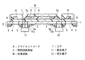
これまで、光電気混載基板は、電気回路基板と光導波路とを個別につくり、両者を接着剤により貼り合わせて形成されていた。例えば、上記光電気混載基板は、図6に示すように、電気回路83が多層に形成された電気回路基板81上に、接着剤82を介して、アンダークラッド層86とコア87とオーバークラッド層88とからなる光導波路80が精度よく貼り合わされている。そして、上記電気回路基板81に形成された実装用パッド(電気回路83の一部)に、発光素子11および受光素子12がフリップチップ実装されている(例えば、特許文献1参照)。図6に示す光電気混載基板では、上記発光素子11および受光素子12がそれぞれ光導波路80の両端部の表面側に位置決めされている。また、上記光導波路80の両端部は、光軸に対して45°傾斜した傾斜面に形成され、その傾斜面のコア87部分が光路変換ミラー87aに形成されている。なお、図6において、符号11aは、上記発光素子11の電極(バンプ)であり、符号12aは、受光素子12の電極(バンプ)である。
Conventionally, an opto-electric hybrid board has been formed by separately making an electric circuit board and an optical waveguide and bonding them together with an adhesive. For example, as shown in FIG. 6, the opto-electric hybrid board includes an under-
上記光電気混載基板における光Lの伝播は、つぎのようにして行われる。まず、発光素子11から光Lが下方に出射される。その光Lは、光導波路80の一端部(図6では左端部)のオーバークラッド層88を通り抜け、コア87の一端部に入射する。つづいて、その光Lは、コア87の一端部の光路変換ミラー87aで反射して(光路が90°変換して)、コア87内を、軸方向に進む。そして、その光Lは、コア87内を進みコア87の他端部(図6では右端部)まで伝播する。つづいて、その光Lは、上記他端部の光路変換ミラー87aで上方に反射し(光路が90°変換し)、オーバークラッド層88を通り抜けて出射され、受光素子12で受光される。
しかしながら、上記特許文献1の光電気混載基板の製造において、実際には、電気回路基板81と光導波路80とを接着剤82で貼り合わせる際に、接着剤82自身の流動性により、貼り合わせの際の圧力が加わると幾分のずれが生じる。このため、上記電気回路基板81の実装用パッドを認識して発光素子11および受光素子12を精度よく上記電気回路基板81に実装したとしても、その電気回路基板81自体にずれが生じているため、光導波路80のコア87両端部の光路変換ミラー87aに対する発光素子11および受光素子12のアライメント(位置決め)精度は低下した状態となる。この状態での光Lの伝播は、上記コア87両端部の光路変換ミラー87aに対して発光素子11および受光素子12の光軸がずれた状態で行われ、光Lの結合損失が大きくなる。
However, in the manufacture of the opto-electric hybrid board described in
本発明は、このような事情に鑑みなされたもので、光導波路のコアに対する光学素子のアライメント精度を向上させることができる光電気混載基板の製造方法の提供をその目的とする。 The present invention has been made in view of such circumstances, and an object thereof is to provide a method for manufacturing an opto-electric hybrid board capable of improving the alignment accuracy of an optical element with respect to a core of an optical waveguide.
上記の目的を達成するため、本発明の光電気混載基板の製造方法は、電気回路基板を準備する工程と、この電気回路基板の回路形成面と反対側の面に光導波路形成用の感光性樹脂層を形成する工程と、上記感光性樹脂層のコア形成領域をフォトリソグラフィ法により所定パターンのコアに形成する工程をもつ光導波路作製工程と、上記光導波路の端部側に対応する上記電気回路基板の回路形成面の部分に光学素子を実装する工程と、上記光導波路の上記端部側に位置するコアの端部を,光を反射して上記コアと上記光学素子との間の光伝播を可能とする反射部に形成する工程と、上記電気回路基板に上記コアと上記光学素子との間の光伝播用の通路を設ける工程とを備え、上記感光性樹脂層としてコア形成領域とともにアライメントマーク形成領域をもつ感光性樹脂層を使用し、上記コアの形成と同時に、上記アライメントマーク形成領域を上記フォトリソグラフィ法により所定パターンのアライメントマークに形成する工程と、上記光学素子の実装を、上記アライメントマークを基準として所定の位置に行う工程とを有するという構成をとる。 In order to achieve the above object, a method for manufacturing an opto-electric hybrid board according to the present invention includes a step of preparing an electric circuit board, and a photosensitive property for forming an optical waveguide on a surface of the electric circuit board opposite to the circuit forming surface. A step of forming a resin layer, a step of forming a core formation region of the photosensitive resin layer on a core having a predetermined pattern by a photolithography method, and a step of forming the optical waveguide corresponding to the end side of the optical waveguide. A step of mounting the optical element on the circuit forming surface of the circuit board; and an end of the core located on the end side of the optical waveguide to reflect light between the core and the optical element. A step of forming a reflection portion that allows propagation; and a step of providing a passage for light propagation between the core and the optical element in the electric circuit board, and as a photosensitive resin layer together with a core formation region Alignment mark type A step of forming the alignment mark forming region on the alignment mark having a predetermined pattern by the photolithography method simultaneously with the formation of the core using a photosensitive resin layer having a region, and mounting the optical element, the alignment mark And a step of performing the process at a predetermined position with reference to the above.
本発明の光電気混載基板の製造方法では、電気回路基板の回路形成面と反対側の面に、コア形成領域とアライメントマーク形成領域とをもつ感光性樹脂層を形成し、その感光性樹脂層から、1回のフォトリソグラフィ法により、コアと、光学素子位置決め用のアライメントマークとを同時に形成し、かつ、上記感光性樹脂層から光導波路を形成している。このため、光導波路を電気回路基板に接着する接着剤が不要となり、接着剤使用による、ずれの不具合が生じなくなると同時に、上記アライメントマークに対するコアの位置を、所定の位置関係に設定することができる。そして、本発明では、上記光学素子の実装を、上記アライメントマークを基準として行うため、上記光学素子を光導波路のコアに対して適正な位置に実装することができる。その結果、製造された光電気混載基板では、コアの端部の光反射部と光学素子との間における光の結合損失を極めて小さくすることができる。 In the method for producing an opto-electric hybrid board according to the present invention, a photosensitive resin layer having a core formation region and an alignment mark formation region is formed on the surface opposite to the circuit formation surface of the electric circuit substrate, and the photosensitive resin layer Thus, the core and the alignment mark for positioning the optical element are formed simultaneously by a single photolithography method, and the optical waveguide is formed from the photosensitive resin layer. This eliminates the need for an adhesive for bonding the optical waveguide to the electric circuit board, eliminates the problem of misalignment due to the use of the adhesive, and at the same time sets the position of the core with respect to the alignment mark to a predetermined positional relationship. it can. In the present invention, the optical element is mounted on the basis of the alignment mark, so that the optical element can be mounted at an appropriate position with respect to the core of the optical waveguide. As a result, in the manufactured opto-electric hybrid board, the coupling loss of light between the light reflecting portion at the end of the core and the optical element can be extremely reduced.
つぎに、本発明の実施の形態を図面にもとづいて詳しく説明する。 Next, embodiments of the present invention will be described in detail with reference to the drawings.
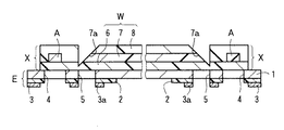
図1は、本発明の光電気混載基板の製造方法の第1の実施の形態によって得られた光電気混載基板を示している。この光電気混載基板は、電気回路3を有する電気回路基板Eと、この電気回路基板Eの電気回路3形成面(裏面)と反対側の面(表面)に形成された光導波路Wを備えている。そして、その電気回路基板Eの裏面では、光導波路Wの端部側に対応する電気回路基板Eの電気回路3形成面の部分に発光素子11および受光素子12が実装されている。なお、上記電気回路基板Eは、ステンレス製基板1の裏面に、絶縁層2を介して、電気回路3を形成して構成され、この電気回路3の一部は、上記発光素子11,受光素子12を実装するための実装用パッド3aとなっている。一方、上記光導波路Wは、上記電気回路基板Eの表面に、アンダークラッド層6を介して、感光性樹脂層を形成し、その感光性樹脂層を加工してコア7を形成し、さらにその上に、オーバークラッド層8を積層形成して構成されている。この光導波路Wの左右両端部は、図示のように、上記ステンレス製基板1に対して45°傾斜した傾斜面に形成されている。そして、その傾斜面に位置するコア7の端部が光反射部7aになっている。この光導波路Wの左右両端側には、上記光導波路Wと同材料からなる3層積層体Xが形成されており、その中間層が上記コア7と同材料からなり、アライメントマークAに形成されている。そして、上記コア7両端部の光反射部7aの下方に対応する上記ステンレス製基板1の部分に、コアと発光素子11,受光素子12との間で光を伝播するための光通過用の貫通孔5が形成され、上記アライメントマークAの下方に対応する上記ステンレス製基板1の部分に、アライメントマークAを裏面側から視認するための視認用の貫通孔4が形成されている。また、上記コア7の一端部(図1では左端部)に形成された光反射部7aの下方では、発光素子11が上記実装用パッド3aに実装されており、上記コア7の他端部(図1では右端部)に形成された光反射部7aの下方では、受光素子12が上記実装用パッド3aに実装されている。
FIG. 1 shows an opto-electric hybrid board obtained by the first embodiment of the opto-electric hybrid board manufacturing method of the present invention. This opto-electric hybrid board includes an electric circuit board E having the
そして、上記コア7両端部の光反射部7aは、光Lを反射して上記コア7と上記発光素子11および受光素子12との間の光伝播を可能にしている。すなわち、上記光電気混載基板では、上記発光素子11は、コア7の一端部の光反射部7aに対して光Lを出射する光学素子であり、その発光素子11から出射された光Lは、上記ステンレス製基板1の光通過用の貫通孔5を通過した後、光導波路Wの一端部のアンダークラッド層4を通り抜け、コア7の一端部に入射する。ついで、その光Lは、上記コア7の一端部の光反射部7aで反射して、コア7内を、軸方向に進む。そして、その光Lは、コア7内を進みコア7の他端部の光反射部7aまで伝播する。つづいて、その光Lは、上記他端部の光反射部7aで下方に反射し、アンダークラッド層6を通り抜けて出射される。そして、その光Lは、上記ステンレス製基板1の光通過用の貫通孔5を通過した後、受光素子12で受光される。
The
この実施の形態の光電気混載基板は、下記の(1)〜(4)の工程を経て製造される。
(1)ステンレス製基板1の裏面に電気回路3を形成して電気回路基板Eを作製する工程〔図2(a)〜(c)参照〕。
(2)上記電気回路基板Eのステンレス製基板1の表面に光導波路Wを作製する工程〔図3(a)〜(d)参照〕。
(3)上記光導波路Wのコア7の両端部を光反射部7aに形成する工程(図4参照)。
(4)上記電気回路3に発光素子11および受光素子12を実装する工程(図1参照)。
The opto-electric hybrid board of this embodiment is manufactured through the following steps (1) to (4).
(1) A step of forming an electric circuit board E by forming an
(2) A step of producing an optical waveguide W on the surface of the
(3) A step of forming both end portions of the
(4) A step of mounting the
上記(1)の電気回路基板Eの作製工程について説明する。この実施の形態では、まず、上記ステンレス製基板1〔図2(a)参照〕を準備する。このステンレス製基板1〔図2(a)参照〕としては、通常、厚みが20〜200μmの範囲内のものが用いられる。 The manufacturing process of the electric circuit board E of (1) will be described. In this embodiment, first, the stainless steel substrate 1 (see FIG. 2A) is prepared. As this stainless steel substrate 1 (see FIG. 2A), a substrate having a thickness in the range of 20 to 200 μm is usually used.
ついで、図2(a)に示すように、上記ステンレス製基板1の裏面の所定位置に、フォトリソグラフィ法により所定パターンの絶縁層2を形成する。この絶縁層2は、後の工程〔図2(c)参照〕でステンレス製基板1に形成されるアライメントマークA視認用の貫通孔4および光通過用の貫通孔5の部分を除いて形成される。すなわち、上記絶縁層2の形成は、つぎのようにして行われる。まず、上記ステンレス製基板1の裏面(絶縁層2の形成時は上に向ける)の所定位置に、感光性ポリイミド樹脂,感光性エポキシ樹脂等の感光性樹脂を塗布し、感光性樹脂層を形成する。ついで、絶縁層2のパターンに対応する開口パターンが形成されているフォトマスクを介して、上記感光性樹脂層を照射線により露光する。つぎに、現像液を用いて現像を行うことにより、未露光部分を溶解させて除去し、残存した感光性樹脂層を絶縁層2のパターンに形成する。その後、その残存感光性樹脂層中の現像液を加熱処理により除去する。これにより、上記残存感光性樹脂層を絶縁層2に形成する。絶縁層2の厚みは、通常、5〜15μmの範囲内に設定される。
Next, as shown in FIG. 2A, an
つぎに、図2(b)に示すように、上記絶縁層2の表面に、実装用パッド3aを含む電気回路3を所定パターンに形成する。すなわち、この電気回路3の形成は、つぎのようにして行われる。まず、上記絶縁層2の表面(電気回路3の形成時は上に向ける)に、スパッタリングまたは無電解めっき等により金属層(厚み600〜2600Å程度)を形成する。この金属層は、後の電解めっきを行う際のシード層(電解めっき層形成の素地となる層)となる。ついで、上記ステンレス製基板1,絶縁層2および金属層(シード層)からなる積層体の両面に、ドライフィルムレジストを貼着した後、上記金属層が形成されている側のドライフィルムレジストに、フォトリソグラフィ法により電気回路3のパターンの溝部を形成し、その溝部の底に上記金属層の表面部分を露呈させる。つぎに、電解めっきにより、上記溝部の底に露呈した上記金属層の表面部分に、電解めっき層(厚み5〜20μm程度)を積層形成する。そして、上記ドライフィルムレジストを水酸化ナトリウム水溶液等により剥離する。その後、上記電解めっき層が形成されていない金属層部分をソフトエッチングにより除去し、残存した電解めっき層とその下の金属層とからなる積層部分を電気回路3に形成する。
Next, as shown in FIG. 2B, an
ついで、図2(c)に示すように、ステンレス製基板1の所定位置に、エッチング等により、アライメントマークA視認用の貫通孔4および光通過用の貫通孔5を形成する。そのアライメントマークA視認用の貫通孔4は、後の光導波路W作製工程でコア7の両端部付近に形成されるアライメントマークAに対応する位置(2個所)に形成され、上記光通過用の貫通孔5は、上記コア7の両端部に対応する位置(2個所)に形成される。すなわち、これら貫通孔4,5の形成は、つぎのようにして行われる。まず、上記ステンレス製基板1,絶縁層2および電気回路3からなる積層体の両面に、ドライフィルムレジストを貼着した後、片面側のドライフィルムレジストに、フォトリソグラフィ法により上記両貫通孔4,5のパターンの孔部を形成し、その孔部の底に上記ステンレス製基板1の表面部分を露呈させる。つぎに、塩化第2鉄水溶液を用いたエッチング等により、上記孔部の底に露呈した上記ステンレス製基板1部分を穿孔し、上記アライメントマークA視認用の貫通孔4および光通過用の貫通孔5を形成する。上記アライメントマークA視認用の貫通孔4の直径は、通常、0.1〜3.0mmの範囲内に設定され、上記光通過用の貫通孔5の直径は、通常、0.05〜0.2mmの範囲内に設定される。但し、これら貫通孔4,5の直径は、アライメントマークAの大きさ,発光素子11等のデザインに左右されるため、必ずしも上記範囲内とは限らない。このようにして、上記(1)の電気回路基板Eの作製工程が完了する。
Next, as shown in FIG. 2C, a through
上記(1)の電気回路基板Eの作製工程につづく上記(2)の光導波路Wの作製工程について説明する。この実施の形態では、まず、図3(a)に示すように、上記ステンレス製基板1の表面の所定位置に、フォトリソグラフィ法により所定パターンのアンダークラッド層6を形成する。すなわち、このアンダークラッド層6の形成は、つぎのようにして行われる。まず、上記ステンレス製基板1の表面の所定位置に、感光性ポリイミド樹脂,感光性エポキシ樹脂等の、アンダークラッド層6形成用の感光性樹脂が溶媒に溶解しているワニスを塗布した後、必要に応じて、それを加熱処理(50〜120℃×10〜30分間程度)して乾燥させ、アンダークラッド層6形成用の感光性樹脂層を形成する。ついで、アンダークラッド層6のパターンに対応する開口パターンが形成されているフォトマスクを介して、上記感光性樹脂層を照射線により露光する。つぎに、現像液を用いて現像を行うことにより、未露光部分を溶解させて除去し、残存した感光性樹脂層をアンダークラッド層6のパターンに形成する。その後、その残存感光性樹脂層中の現像液を加熱処理により除去する。これにより、上記残存感光性樹脂層をアンダークラッド層6に形成する。アンダークラッド層6の厚みは、通常、5〜50μmの範囲内に設定される。
The manufacturing process of the optical waveguide W of the above (2) following the manufacturing process of the electric circuit board E of the above (1) will be described. In this embodiment, first, as shown in FIG. 3A, an
ついで、図3(b)〜(c)に示すように、上記アンダークラッド層6の表面の所定位置に、コア7形成領域とアライメントマークA形成領域とをもつ感光性樹脂層7Aから、1回のフォトリソグラフィ法により、所定パターンのコア7と光学素子位置決め用のアライメントマークAとを同時に形成する。これが本発明の特徴の一つである。本発明では、上記のようにしてコア7と同時に光学素子位置決め用のアライメントマークAを形成することにより、次々工程(4)の光学素子(発光素子11および受光素子12)実装工程において、上記アライメントマークAを基準として、光導波路Wのコア7に対して適正な位置に、発光素子11および受光素子12を実装することができるようになる。
Next, as shown in FIGS. 3B to 3C, once from the
この実施の形態では、コア7の両端部付近にそれぞれ一つのアライメントマークAを形成する。より詳しく説明すると、これらコア7およびアライメントマークAの形成は、つぎのようにして行われる。まず、図3(b)に示すように、上記アンダークラッド層6の表面の所定位置に、上記コア7およびアライメントマークA形成用の感光性樹脂が溶媒に溶解しているワニスを塗布した後、必要に応じて、それを加熱処理(50〜120℃×10〜30分間程度)して乾燥させ、コア7形成用の感光性樹脂層7Aを形成する。ついで、コア7およびアライメントマークAのパターンに対応する開口パターンが形成されているフォトマスクMを介して、上記感光性樹脂層を照射線Rにより露光した後、上記アンダークラッド層6の形成と同様に現像,加熱処理等を行う。このようなフォトリソグラフィ法により、図3(c)に示すように、所定パターンのコア7およびアライメントマークAを形成する。この実施の形態では、上記アライメントマークA視認用の貫通孔4の上方にアライメントマークAを位置決め形成し、上記光通過用の貫通孔5の上方にコアの各端部を位置決め形成する。コア7の厚みは、通常、5〜60μmの範囲内に設定され、その幅は、通常、5〜60μmの範囲内に設定される。また、アライメントマークAは、通常、平面視十字状に形成され、その厚みは、通常、5〜60μmの範囲内に設定され、その十字状のライン幅は、通常、0.02〜0.2mmの範囲内に設定され、十字状の縦横の長さは、通常、0.2〜1.0mmの範囲内に設定される。なお、上記コア7およびアライメントマークAの形成材料としては、例えば、上記アンダークラッド層6と同様の感光性樹脂があげられ、上記アンダークラッド層6および下記オーバークラッド層8の形成材料よりも屈折率が大きい材料が用いられる。この屈折率の調整は、例えば、上記アンダークラッド層6,コア7(アライメントマークAを含む),オーバークラッド層8の各形成材料の種類の選択や組成比率を調整して行うことができる。
In this embodiment, one alignment mark A is formed in the vicinity of both ends of the
つぎに、図3(d)に示すように、上記コア7およびアライメントマークAを被覆した状態で、上記アンダークラッド層6の表面に、フォトリソグラフィ法により所定パターンのオーバークラッド層8を形成する。すなわち、このオーバークラッド層8の形成は、つぎのようにして行われる。まず、上記コア7を被覆するように、オーバークラッド層8形成用の感光性樹脂が溶媒に溶解しているワニスを塗布した後、必要に応じて、それを加熱処理(50〜120℃×10〜30分間程度)して乾燥させ、オーバークラッド層8形成用の感光性樹脂層を形成する。ついで、オーバークラッド層8のパターンに対応する開口パターンが形成されているフォトマスクを用いたフォトリソグラフィ法により、所定パターンのオーバークラッド層8を形成する。このオーバークラッド層8の厚みは、通常、10〜2000μmの範囲内に設定される。なお、上記オーバークラッド層8の形成材料としては、例えば、上記アンダークラッド層6と同様の感光性樹脂があげられる。このようにして、上記(2)の光導波路Wの作製工程が完了する。
Next, as shown in FIG. 3D, an over
上記(2)の光導波路Wの作製工程につづく上記(3)の光反射部7aの形成工程について説明する。すなわち、この光反射部7aの形成は、図4に示すように、上記コア7の両端部に対応する光導波路Wの両端部を、レーザ加工または刃先角度45°の回転刃等を用いた切削加工等により、上記ステンレス製基板1に対して45°傾斜した傾斜面に形成することにより行われる。そして、その傾斜面のコア7部分が光反射部(光路変換ミラー)7aとして作用する。この光反射部7aでは、コア7の屈折率の方が、上記光反射部7aの外側にある空気の屈折率よりも大きいため、光反射部7aに当たった光は、その大部分が反射する。また、上記のように光導波路Wの両端部が傾斜面に形成されることにより、上記光導波路Wの両端側に、上記アライメントマークAを中間層に有する3層積層体Xが形成される。このようにして、上記(3)の光反射部7aの形成工程が完了する。
The step (3) of forming the
上記(3)の光反射部7aの形成工程につづく上記(4)の光学素子実装工程について説明する。すなわち、この光学素子(発光素子11および受光素子12)の実装は、つぎのようにして行われる。まず、上記光反射部7aまで形成された生産中間物を、電気回路3側の面を上に向けて実装機のステージ上にセットする。そして、その実装機に備えられている画像認識装置により、一方(例えば図1の左側)のアライメントマークAを、アンダークラッド層6およびアライメントマークA視認用の貫通孔4を通して視認する(読み取る)。これにより、上記実装機は、上記アライメントマークAを基準として、そのアライメントマークAに近い上記コア7の一端部の光反射部7aの位置を算出する。そして、図1に示すように、その算出した光反射部7aの位置に、一方の光学素子(例えば発光素子11)の光軸が合わさるよう、その光学素子を、上記光通過用の貫通孔5の下方を覆うようにして実装用パッド3aに実装する。他方(例えば図1の右側)のアライメントマークAも、同様に、他方の光学素子(例えば受光素子12)を実装する際に、その実装の位置決め基準として利用される。上記発光素子11としては、VCSEL(Vertical Cavity Surface Emitting Laser)等があげられ、受光素子12としては、PD(Photo Diode )等があげられる。このように、上記アライメントマークAを基準として、上記発光素子11および受光素子12を所定の位置に実装することが本発明の特徴の一つである。なお、図1において、符号11aは、上記発光素子11の電極(バンプ)であり、符号12aは、受光素子12の電極(バンプ)である。
The optical element mounting step (4) following the step (3) for forming the
上記発光素子11および受光素子12の実装方法としては、フリップチップ,半田リフロー,半田バンプと半田ペーストのスクリーン印刷によるC4接合等があげられる。なかでも、実装の際の位置ずれが小さくできる観点から、超音波や加熱によるフリップチップが好ましく、より好ましくは、上記ステンレス製基板1に熱によるダメージを与えないようにする観点から、超音波によるフリップチップである。このようにして、上記(4)の光学素子実装工程が完了し、目的とする光電気混載基板が得られる。
Examples of the mounting method of the
このように、上記光電気混載基板の製造方法では、電気回路基板Eの表面に、コア7形成用の感光性樹脂層7A(図3(b)参照)を形成し、その感光性樹脂層7AにアライメントマークA形成領域を設け、その感光性樹脂層7Aから、1回のフォトリソグラフィ法により、コア7と同時に、発光素子11および受光素子12位置決め用のアライメントマークAを形成する。そして、そのアライメントマークAを目印にして所定の位置に発光素子11および受光素子12を実装する。このため、光導波路Wのコア7に対する発光素子11および受光素子12のアライメント精度を向上させることができる。その結果、製造された光電気混載基板では、コア7の各端部の光反射部7aと発光素子11,受光素子12との間における光の結合損失を小さくすることができる。
As described above, in the method for manufacturing an opto-electric hybrid board, the
また、上記実施の形態では、基板1として、ステンレス製のものを用いているため、そのステンレス製基板1は、熱に対する伸縮耐性に優れたものとなっている。このため、上記ステンレス製基板1に穿孔されたアライメントマークA視認用の貫通孔4と光通過用の貫通孔5との位置関係、および上記ステンレス製基板1上に作製された光導波路Wの寸法等は、設計値に略維持される。すなわち、ステンレス製基板1は、上記アライメントマークAを基準とする、コア7の両端部の光反射部7aと発光素子11および受光素子12とのアライメント精度向上にとって、基板1として好ましいものとなっている。
Moreover, in the said embodiment, since the thing made from stainless steel is used as the board |
なお、上記ステンレス製基板1に代えて、他の金属材料または樹脂材料等からなる基板1を用いてもよい。その基板1が絶縁性を有するものである場合は、上記絶縁層2を形成することなく、上記基板1に直接、電気回路3を形成してもよい。上記絶縁層2は、上記金属製基板1のような通電性を有する基板1と電気回路3との短絡を防止するためのものである。
Instead of the
また、上記実施の形態では、アンダークラッド層6を形成したが、アンダークラッド層6を形成することなく、ステンレス製基板1等の基板1の表面に直接、コア7およびアライメントマークAを形成してもよい。
In the above embodiment, the under
図5は、本発明の光電気混載基板の製造方法の第2の実施の形態を示している。この実施の形態は、上記第1の実施の形態において、光導波路Wの両端部の傾斜面の表面に、金属膜9を、めっきまたは蒸着により形成する形態である。これにより製造された光電気混載基板では、光反射部7aの外側表面が上記金属膜9で被覆されるため、光反射部7aでの光の反射率を高めることができ、光の伝播効率を高めることができる。それ以外の部分は上記第1の実施の形態と同様であり、同様の部分には同じ符号を付している。
FIG. 5 shows a second embodiment of the method for manufacturing an opto-electric hybrid board according to the present invention. In this embodiment, in the first embodiment, the
上記金属膜9の形成は、例えば、上記光導波路Wの両端部の傾斜面以外の部分をレジスト層によりマスキングした状態(上記傾斜面のみを露呈した状態)で、上記めっきまたは蒸着により行われる。その後、上記レジスト層は除去される。上記金属膜9の厚みは、例えば、50nm〜5μmの範囲内に設定される。上記金属膜9の形成材料としては、例えば、ニッケル,銅,銀,金,クロム,アルミニウム,亜鉛,錫,コバルト,タングステン,白金,パラジウムおよびこれらの2種以上の元素を含む合金材料等があげられる。なお、上記金属膜9の形成は、発光素子11および受光素子12の実装に先立って行うことが好ましい。
The
つぎに、実施例について説明する。但し、本発明は、これに限定されるわけではない。 Next, examples will be described. However, the present invention is not limited to this.
〔電気回路基板の形成〕
ステンレス製基板(厚み20μmのSUS304箔)の片面に、まず、フォトリソグラフィ法により、感光性ポリイミド樹脂からなる絶縁層(厚み10μm)を所定パターンに形成した。ついで、上記絶縁層の表面にスパッタリングにより、銅/ニッケル/クロム合金からなるシード層を形成した。つぎに、上記ステンレス製基板,絶縁層およびシード層からなる積層体の両面に、ドライフィルムレジストを貼着した後、上記シード層が形成されている側の上記ドライフィルムレジストに、フォトリソグラフィ法により、実装用パッドを含む電気回路のパターンの溝部を形成し、その溝部の底に上記シード層の表面部分を露呈させた。つぎに、電解銅めっきにより、上記溝部の底に露呈した上記シード層の表面部分に、電解銅めっき層(厚み20μm)を積層形成した。そして、上記ドライフィルムレジストを水酸化ナトリウム水溶液により剥離した。その後、上記電解銅めっき層が形成されていないシード層部分をソフトエッチングにより除去し、残存した電解銅めっき層とその下のシード層とからなる積層部分を電気回路に形成した。さらに、上記ステンレス製基板,絶縁層および電気回路からなる積層体の両面に、ドライフィルムレジストを貼着した後、片面側の上記ドライフィルムレジストに、フォトリソグラフィ法によりアライメントマーク視認用の貫通孔および光通過用の貫通孔のパターンの孔部を形成し、その孔部の底に上記ステンレス製基板の表面部分を露呈させた。つぎに、塩化第2鉄水溶液を用いたエッチングにより、上記孔部の底に露呈した上記ステンレス製基板部分を穿孔し、上記アライメントマーク視認用の貫通孔および光通過用の貫通孔をそれぞれ2個形成した。その後、上記実装用パッドの表面に、金/ニッケル合金めっき層を形成した。
[Formation of electric circuit board]
First, an insulating layer (thickness 10 μm) made of a photosensitive polyimide resin was formed in a predetermined pattern on one side of a stainless steel substrate (SUS 304 foil having a thickness of 20 μm) by photolithography. Next, a seed layer made of a copper / nickel / chromium alloy was formed on the surface of the insulating layer by sputtering. Next, after applying a dry film resist on both surfaces of the laminate made of the stainless steel substrate, the insulating layer and the seed layer, the photolithography method is applied to the dry film resist on the side where the seed layer is formed. Then, a groove portion of an electric circuit pattern including a mounting pad was formed, and the surface portion of the seed layer was exposed at the bottom of the groove portion. Next, an electrolytic copper plating layer (thickness 20 μm) was formed on the surface portion of the seed layer exposed at the bottom of the groove by electrolytic copper plating. And the said dry film resist was peeled with the sodium hydroxide aqueous solution. Thereafter, the seed layer portion where the electrolytic copper plating layer was not formed was removed by soft etching, and a laminated portion including the remaining electrolytic copper plating layer and the seed layer therebelow was formed in an electric circuit. Furthermore, after pasting a dry film resist on both surfaces of the laminate made of the stainless steel substrate, the insulating layer and the electric circuit, the through hole for visually recognizing the alignment mark by the photolithography method on the dry film resist on one side and A hole portion having a pattern of through holes for passing light was formed, and the surface portion of the stainless steel substrate was exposed at the bottom of the hole portion. Next, the stainless steel substrate portion exposed at the bottom of the hole is drilled by etching using a ferric chloride aqueous solution, and the alignment mark visual recognition through hole and the light passage through hole are each provided with two holes. Formed. Thereafter, a gold / nickel alloy plating layer was formed on the surface of the mounting pad.
〔アンダークラッド層およびオーバークラッド層の形成材料〕
下記の一般式(1)で示されるビスフェノキシエタノールフルオレングリシジルエーテル(成分A)35重量部、脂環式エポキシである3,4−エポキシシクロヘキセニルメチル−3’,4’−エポキシヘキセンカルボキシレート(ダイセル化学社製、セロキサイド2021P)(成分B)40重量部、シクロヘキセンオキシド骨格を有する脂環式エポキシ樹脂(ダイセル化学社製、セロキサイド2081)(成分C)25重量部、4,4’−ビス〔ジ(βヒドロキシエトキシ)フェニルスルフィニオ〕フェニルスルフィド−ビス−ヘキサフルオロアンチモネートの50%プロピオンカーボネート溶液(成分D)2重量部とを混合することにより、アンダークラッド層およびオーバークラッド層の形成材料を調製した。
[Formation material of under clad layer and over clad layer]
35 parts by weight of bisphenoxyethanol fluorene glycidyl ether (component A) represented by the following general formula (1), 3,4-epoxycyclohexenylmethyl-3 ′, 4′-epoxyhexene carboxylate (Daicel) which is an alicyclic epoxy Chemical Co., Celoxide 2021P) (Component B) 40 parts by weight, cycloaliphatic epoxy resin having a cyclohexene oxide skeleton (Daicel Chemical Co., Celoxide 2081) (Component C) 25 parts by weight, 4,4′-bis [di (Β-Hydroxyethoxy) phenylsulfinio] phenyl sulfide-bis-hexafluoroantimonate 50% propionate carbonate solution (component D) 2 parts by weight were mixed to form a material for forming the under-cladding layer and the over-cladding layer. Prepared.

〔コアの形成材料〕
上記成分A:70重量部、1,3,3−トリス{4−〔2−(3−オキセタニル)〕ブトキシフェニル}ブタン:30重量部、上記成分D:1重量部を乳酸エチルに溶解することにより、コアの形成材料を調製した。
[Core forming material]
Component A: 70 parts by weight, 1,3,3-tris {4- [2- (3-oxetanyl)] butoxyphenyl} butane: 30 parts by weight, Component D: 1 part by weight dissolved in ethyl lactate Thus, a core forming material was prepared.
〔光導波路の作製〕
上記ステンレス製基板のもう一方の片面(上記電気回路が形成された面とは反対側の面)に、上記アンダークラッド層の形成材料を塗布し、塗布層を形成した。その後、その塗布層の全面に、超高圧水銀灯を用いて積算光量1000mJ/cm2 (i線基準)の露光を行い、上記塗布層を硬化させた。つづいて、120℃×15分間のベーキング(加熱処理)を行うことにより、発生した酸を拡散させ、反応を完了させた。このようにしてアンダークラッド層(厚み10μm)を形成した。
[Production of optical waveguide]
The undercladding layer forming material was applied to the other surface of the stainless steel substrate (the surface opposite to the surface on which the electric circuit was formed) to form a coating layer. Thereafter, the entire surface of the coating layer was exposed to an integrated light amount of 1000 mJ / cm 2 (i-line basis) using an ultra-high pressure mercury lamp to cure the coating layer. Subsequently, the generated acid was diffused by baking (heat treatment) at 120 ° C. for 15 minutes to complete the reaction. In this way, an under cladding layer (thickness 10 μm) was formed.
そして、上記アンダークラッド層の表面に、コアの形成材料を塗布した後、70℃×5分間のベーキングを行うことにより、溶媒を揮発させ、コア形成用の感光性樹脂層を形成した。ついで、その上方に、形成するコアとアライメントマークのパターンと同形状の開口パターンが形成されたフォトマスクを、アライメントマーク視認用の貫通孔にアライメントマークが、光通過用の貫通孔にコアの各端部が、それぞれ重なって形成されるように、位置決めした。そして、そのフォトマスクを介して、積算光量2000mJ/cm2 (i線基準)の露光を行うことにより、上記感光性樹脂層の露光部分を硬化させた。つづいて、120℃×15分間のベーキング(加熱処理)を行うことにより、発生した酸を拡散させ、反応を完了させた。つぎに、γ−ブチロラクトン水溶液(現像液)中で洗浄(現像)し、未露光部分を溶解除去した。その後、120℃×15分間のベーキングを行うことにより、コア(幅50μm×高さ50μm)および十字状のアライメントマーク(十字状のライン幅0.05mm、十字状の縦の長さ0.5mm、十字状の横の長さ0.5mm、高さ50μm)を形成した。 And after apply | coating the formation material of a core to the surface of the said under clad layer, the solvent was volatilized by baking for 70 degreeC x 5 minutes, and the photosensitive resin layer for core formation was formed. Next, a photomask in which an opening pattern having the same shape as the core and alignment mark pattern to be formed is formed above the alignment mark in the through hole for viewing the alignment mark, and each of the core in the through hole for passing light. The end portions were positioned so as to overlap each other. And the exposed part of the said photosensitive resin layer was hardened by performing exposure of the integrated light quantity 2000mJ / cm < 2 > (i line reference | standard) through the photomask. Subsequently, the generated acid was diffused by baking (heat treatment) at 120 ° C. for 15 minutes to complete the reaction. Next, it was washed (developed) in a γ-butyrolactone aqueous solution (developer), and the unexposed portion was dissolved and removed. Thereafter, by baking at 120 ° C. for 15 minutes, the core (width 50 μm × height 50 μm) and the cross-shaped alignment mark (cross-shaped line width 0.05 mm, cross-shaped vertical length 0.5 mm, A cross-shaped horizontal length of 0.5 mm and a height of 50 μm was formed.
ついで、上記コアを被覆するように、上記オーバークラッド層の形成材料を塗布し、塗布層を形成した。その後、その塗布層の全面に、超高圧水銀灯を用いて積算光量1000mJ/cm2 (i線基準)の露光を行い、上記塗布層を硬化させた。つづいて、120℃×15分間のベーキング(加熱処理)を行うことにより、発生した酸を拡散させ、反応を完了させた。このようにしてオーバークラッド層を形成し、上記ステンレス製基板の、電気回路が形成された面とは反対側の面に、光導波路(総厚75μm)を作製した。 Subsequently, the over clad layer forming material was applied so as to cover the core, thereby forming an application layer. Thereafter, the entire surface of the coating layer was exposed to an integrated light amount of 1000 mJ / cm 2 (i-line basis) using an ultra-high pressure mercury lamp to cure the coating layer. Subsequently, the generated acid was diffused by baking (heat treatment) at 120 ° C. for 15 minutes to complete the reaction. In this way, an over clad layer was formed, and an optical waveguide (total thickness 75 μm) was produced on the surface of the stainless steel substrate opposite to the surface on which the electric circuit was formed.
〔光反射部の形成〕
上記光通過用の貫通孔に対応する光導波路の両端部を、エキシマレーザ(光源KrF:波長248nm)によるレーザ加工により、上記ステンレス製基板に対して45°傾斜した傾斜面に形成した。その後、エタノール中で超音波洗浄を行った。上記傾斜面のコア部分が光反射部である。
(Formation of light reflecting part)
Both ends of the optical waveguide corresponding to the through hole for light passage were formed on inclined surfaces inclined by 45 ° with respect to the stainless steel substrate by laser processing using an excimer laser (light source KrF: wavelength 248 nm). Thereafter, ultrasonic cleaning was performed in ethanol. The core portion of the inclined surface is a light reflecting portion.
〔発光素子および受光素子の実装〕
上記光反射部まで形成された生産中間物を、電気回路側の面を上に向けて実装機のステージ上にセットした。そして、その実装機に備えられている画像認識装置により、上記ステンレス製基板に形成されたアライメントマーク視認用の貫通孔を通して上記アライメントマークを視認した状態で、そのアライメントマークを基準として算出される上記コアの光反射部の位置に、発光素子および受光素子の光軸が合わさるよう、上記発光素子および受光素子を、上記光通過用の貫通孔の下方を覆うように実装した。このようにして、光電気混載基板を製造することができた。
[Mounting of light emitting element and light receiving element]
The production intermediate formed up to the light reflecting portion was set on the stage of the mounting machine with the surface on the electric circuit side facing up. Then, by the image recognition device provided in the mounting machine, the alignment mark is calculated with reference to the alignment mark in a state where the alignment mark is visually recognized through the alignment mark visual recognition through hole formed on the stainless steel substrate. The light emitting element and the light receiving element were mounted so as to cover the light passage through hole so that the optical axes of the light emitting element and the light receiving element were aligned with the position of the light reflecting portion of the core. In this way, an opto-electric hybrid board could be manufactured.
A アライメントマーク
E 電気回路基板
W 光導波路
7 コア
11 発光素子
12 受光素子
A alignment mark E electric circuit board W
Claims (4)
Priority Applications (6)
| Application Number | Priority Date | Filing Date | Title |
|---|---|---|---|
| JP2008114329A JP5055193B2 (en) | 2008-04-24 | 2008-04-24 | Manufacturing method of opto-electric hybrid board |
| US12/428,669 US8142672B2 (en) | 2008-04-24 | 2009-04-23 | Manufacturing method of opto-electric hybrid board |
| AT09158611T ATE523803T1 (en) | 2008-04-24 | 2009-04-23 | PRODUCTION METHOD FOR AN OPTOELECTRIC HYBRID PLATE |
| EP09158611A EP2112534B1 (en) | 2008-04-24 | 2009-04-23 | Manufacturing method of opto-electric hybrid board |
| KR1020090035369A KR101560404B1 (en) | 2008-04-24 | 2009-04-23 | Optical/electrical hybrid substrate producing method |
| CN200910135371XA CN101566706B (en) | 2008-04-24 | 2009-04-24 | Manufacturing method of opto-electric hybrid board |
Applications Claiming Priority (1)
| Application Number | Priority Date | Filing Date | Title |
|---|---|---|---|
| JP2008114329A JP5055193B2 (en) | 2008-04-24 | 2008-04-24 | Manufacturing method of opto-electric hybrid board |
Publications (2)
| Publication Number | Publication Date |
|---|---|
| JP2009265342A true JP2009265342A (en) | 2009-11-12 |
| JP5055193B2 JP5055193B2 (en) | 2012-10-24 |
Family
ID=40901955
Family Applications (1)
| Application Number | Title | Priority Date | Filing Date |
|---|---|---|---|
| JP2008114329A Expired - Fee Related JP5055193B2 (en) | 2008-04-24 | 2008-04-24 | Manufacturing method of opto-electric hybrid board |
Country Status (6)
| Country | Link |
|---|---|
| US (1) | US8142672B2 (en) |
| EP (1) | EP2112534B1 (en) |
| JP (1) | JP5055193B2 (en) |
| KR (1) | KR101560404B1 (en) |
| CN (1) | CN101566706B (en) |
| AT (1) | ATE523803T1 (en) |
Cited By (15)
| Publication number | Priority date | Publication date | Assignee | Title |
|---|---|---|---|---|
| JP2012133171A (en) * | 2010-12-22 | 2012-07-12 | Nitto Denko Corp | Method for manufacturing optical waveguide |
| JP2012155215A (en) * | 2011-01-27 | 2012-08-16 | Nitto Denko Corp | Manufacturing method of optical waveguide and optical waveguide body used for the same |
| JP2012194287A (en) * | 2011-03-15 | 2012-10-11 | Sumitomo Bakelite Co Ltd | Manufacturing method for opto-electric hybrid substrate, opto-electric hybrid substrate, and electronic apparatus |
| EP2639612A1 (en) | 2012-03-16 | 2013-09-18 | Nitto Denko Corporation | Opto-electric hybrid board and method of manufacturing same |
| EP2639610A1 (en) | 2012-03-16 | 2013-09-18 | Nitto Denko Corporation | Opto-electric hybrid board and method of manufacturing same |
| EP2662716A1 (en) | 2012-05-08 | 2013-11-13 | Nitto Denko Corporation | Opto-electric hybrid board and method of manufacturing same |
| EP2685794A1 (en) * | 2012-07-13 | 2014-01-15 | Nitto Denko Corporation | Opto-electric hybrid board |
| EP2736309A1 (en) | 2012-11-27 | 2014-05-28 | Nitto Denko Corporation | Opto-electric hybrid board and method of manufacturing same |
| JP2014182208A (en) * | 2013-03-18 | 2014-09-29 | Fujitsu Ltd | Manufacturing method and manufacturing device for optical transmission apparatuses, and optical transmission apparatus |
| WO2014196252A1 (en) * | 2013-06-06 | 2014-12-11 | 日東電工株式会社 | Opto-electric hybrid substrate |
| WO2015064355A1 (en) * | 2013-10-29 | 2015-05-07 | 日東電工株式会社 | Opto-electric hybrid substrate and method for producing same |
| KR20170076655A (en) | 2014-10-24 | 2017-07-04 | 닛토덴코 가부시키가이샤 | Optical/electric hybrid substrate, and production method therefor |
| KR20170076685A (en) | 2014-10-28 | 2017-07-04 | 닛토덴코 가부시키가이샤 | Optical-electric hybrid circuit board |
| KR20170087871A (en) | 2014-11-25 | 2017-07-31 | 닛토덴코 가부시키가이샤 | Opto-electric hybrid substrate and method for producing same |
| WO2021161915A1 (en) * | 2020-02-12 | 2021-08-19 | 日東電工株式会社 | Optical-electric mixed board and optical-electric composite transmission module |
Families Citing this family (26)
| Publication number | Priority date | Publication date | Assignee | Title |
|---|---|---|---|---|
| JP5049145B2 (en) * | 2008-01-22 | 2012-10-17 | 日東電工株式会社 | Manufacturing method of optical waveguide device |
| JP5138459B2 (en) * | 2008-05-15 | 2013-02-06 | 新光電気工業株式会社 | Wiring board manufacturing method |
| JP5106348B2 (en) * | 2008-10-28 | 2012-12-26 | 日東電工株式会社 | Manufacturing method of opto-electric hybrid module and opto-electric hybrid module obtained thereby |
| JP4796615B2 (en) * | 2008-11-26 | 2011-10-19 | 日東電工株式会社 | Opto-electric hybrid board and manufacturing method thereof |
| JP2012208306A (en) * | 2011-03-29 | 2012-10-25 | Nitto Denko Corp | Optoelectric hybrid substrate and manufacturing method thereof |
| US9182544B2 (en) | 2011-12-21 | 2015-11-10 | Intel Corporation | Fabrication of planar light-wave circuits (PLCS) for optical I/O |
| WO2013101112A1 (en) | 2011-12-29 | 2013-07-04 | Intel Corporation | Two-dimensional, high-density optical connector |
| US9507086B2 (en) | 2011-12-30 | 2016-11-29 | Intel Corporation | Optical I/O system using planar light-wave integrated circuit |
| JP5877749B2 (en) * | 2012-03-29 | 2016-03-08 | 日東電工株式会社 | Manufacturing method of opto-electric hybrid board |
| CN103389546B (en) * | 2012-05-08 | 2016-12-07 | 鸿富锦精密工业(深圳)有限公司 | Optical fiber module |
| JP6081086B2 (en) * | 2012-06-14 | 2017-02-15 | Tdk株式会社 | Mounting device and mounting method for photoelectric element |
| AT513747B1 (en) | 2013-02-28 | 2014-07-15 | Mikroelektronik Ges Mit Beschränkter Haftung Ab | Assembly process for circuit carriers and circuit carriers |
| CN104101958B (en) * | 2013-04-03 | 2017-10-03 | 赛恩倍吉科技顾问(深圳)有限公司 | optical communication device |
| JP2014216377A (en) * | 2013-04-23 | 2014-11-17 | イビデン株式会社 | Electronic component, manufacturing method of the same, and manufacturing method of multilayer printed board |
| TWI572933B (en) * | 2013-05-20 | 2017-03-01 | 鴻海精密工業股份有限公司 | Optical communication device |
| AT514599B1 (en) * | 2013-07-05 | 2015-02-15 | Melecs Ews Gmbh & Co Kg | Method for equipping electronic circuit boards with optical components |
| CN106537615B (en) | 2014-08-04 | 2019-08-20 | 株式会社富士 | Mounting device |
| JP6525240B2 (en) * | 2014-10-24 | 2019-06-05 | 日東電工株式会社 | Opto-electric hybrid board and its manufacturing method |
| CN104698552B (en) * | 2015-03-16 | 2016-05-11 | 中国航天科技集团公司第九研究院第七七一研究所 | A kind of for light interconnect substrates and manufacture method thereof on spacecraft and military computer |
| DE102015207709A1 (en) * | 2015-04-27 | 2016-10-27 | Automotive Lighting Reutlingen Gmbh | Method and device for arranging a circuit carrier with a semiconductor light source in a specific position relative to an optical system of a lighting device |
| US9739942B2 (en) * | 2015-10-26 | 2017-08-22 | Kyocera Corporation | Method for manufacturing optical circuit board |
| JP6649076B2 (en) * | 2015-10-26 | 2020-02-19 | 京セラ株式会社 | Manufacturing method of optical circuit board |
| JP7002886B2 (en) * | 2017-08-22 | 2022-01-20 | 日東電工株式会社 | Optical Waveguide, Opto-Electricity Consolidation Board, and Opto-Electricity Consolidation Module |
| JP6677232B2 (en) * | 2017-09-29 | 2020-04-08 | 日亜化学工業株式会社 | Light emitting device manufacturing method |
| JP7489756B2 (en) * | 2018-07-25 | 2024-05-24 | 日東電工株式会社 | Optical element device and manufacturing method thereof |
| US10775573B1 (en) * | 2019-04-03 | 2020-09-15 | International Business Machines Corporation | Embedding mirror with metal particle coating |
Citations (4)
| Publication number | Priority date | Publication date | Assignee | Title |
|---|---|---|---|---|
| JP2000298217A (en) * | 1999-04-13 | 2000-10-24 | Toppan Printing Co Ltd | Optical-electric wiring substrate and manufacture therefor, and mounting substrate |
| JP2004361858A (en) * | 2003-06-06 | 2004-12-24 | Sharp Corp | Optical waveguide with micro lens and its manufacturing method |
| JP2006030798A (en) * | 2004-07-20 | 2006-02-02 | Shinko Electric Ind Co Ltd | Manufacturing method of optical module and manufacturing method of optical propagation member |
| JP2006140233A (en) * | 2004-11-10 | 2006-06-01 | Ibiden Co Ltd | Optical and electrical wiring board and device for optical communication |
Family Cites Families (5)
| Publication number | Priority date | Publication date | Assignee | Title |
|---|---|---|---|---|
| JP2000199827A (en) | 1998-10-27 | 2000-07-18 | Sony Corp | Optical wave guide device and its manufacture |
| TW451084B (en) * | 1999-06-25 | 2001-08-21 | Toppan Printing Co Ltd | Optical-electro wiring board, mounted board, and manufacturing method of optical-electro wiring board |
| EP1122561A1 (en) * | 2000-02-03 | 2001-08-08 | Corning Incorporated | High precision alignment of optical devices over a high thickness transparent layer |
| JP2006120956A (en) | 2004-10-22 | 2006-05-11 | Ibiden Co Ltd | Multilayer printed-wiring board |
| JP2007173375A (en) | 2005-12-20 | 2007-07-05 | Nec Corp | Compound packaging device and manufacturing method thereof |
-
2008
- 2008-04-24 JP JP2008114329A patent/JP5055193B2/en not_active Expired - Fee Related
-
2009
- 2009-04-23 KR KR1020090035369A patent/KR101560404B1/en active IP Right Grant
- 2009-04-23 US US12/428,669 patent/US8142672B2/en not_active Expired - Fee Related
- 2009-04-23 EP EP09158611A patent/EP2112534B1/en not_active Not-in-force
- 2009-04-23 AT AT09158611T patent/ATE523803T1/en not_active IP Right Cessation
- 2009-04-24 CN CN200910135371XA patent/CN101566706B/en not_active Expired - Fee Related
Patent Citations (4)
| Publication number | Priority date | Publication date | Assignee | Title |
|---|---|---|---|---|
| JP2000298217A (en) * | 1999-04-13 | 2000-10-24 | Toppan Printing Co Ltd | Optical-electric wiring substrate and manufacture therefor, and mounting substrate |
| JP2004361858A (en) * | 2003-06-06 | 2004-12-24 | Sharp Corp | Optical waveguide with micro lens and its manufacturing method |
| JP2006030798A (en) * | 2004-07-20 | 2006-02-02 | Shinko Electric Ind Co Ltd | Manufacturing method of optical module and manufacturing method of optical propagation member |
| JP2006140233A (en) * | 2004-11-10 | 2006-06-01 | Ibiden Co Ltd | Optical and electrical wiring board and device for optical communication |
Cited By (36)
| Publication number | Priority date | Publication date | Assignee | Title |
|---|---|---|---|---|
| US9110237B2 (en) | 2010-12-22 | 2015-08-18 | Nitto Denko Corporation | Method of manufacturing optical waveguide |
| JP2012133171A (en) * | 2010-12-22 | 2012-07-12 | Nitto Denko Corp | Method for manufacturing optical waveguide |
| JP2012155215A (en) * | 2011-01-27 | 2012-08-16 | Nitto Denko Corp | Manufacturing method of optical waveguide and optical waveguide body used for the same |
| JP2012194287A (en) * | 2011-03-15 | 2012-10-11 | Sumitomo Bakelite Co Ltd | Manufacturing method for opto-electric hybrid substrate, opto-electric hybrid substrate, and electronic apparatus |
| US8768114B2 (en) | 2012-03-16 | 2014-07-01 | Nitto Denko Corporation | Opto-electric hybrid board and method of manufacturing same |
| EP2639612A1 (en) | 2012-03-16 | 2013-09-18 | Nitto Denko Corporation | Opto-electric hybrid board and method of manufacturing same |
| EP2639610A1 (en) | 2012-03-16 | 2013-09-18 | Nitto Denko Corporation | Opto-electric hybrid board and method of manufacturing same |
| KR20130105360A (en) | 2012-03-16 | 2013-09-25 | 닛토덴코 가부시키가이샤 | Optoelectric hybrid substrate and manufacturing method thereof |
| KR20130105359A (en) | 2012-03-16 | 2013-09-25 | 닛토덴코 가부시키가이샤 | Optoelectric hybrid substrate and method for producing the same |
| US9046646B2 (en) | 2012-03-16 | 2015-06-02 | Nitto Denko Corporation | Opto-electric hybrid board and method of manufacturing same |
| US8837874B2 (en) | 2012-05-08 | 2014-09-16 | Nitto Denko Corporation | Opto-electric hybrid board and method of manufacturing same |
| EP2662716A1 (en) | 2012-05-08 | 2013-11-13 | Nitto Denko Corporation | Opto-electric hybrid board and method of manufacturing same |
| JP2014021203A (en) * | 2012-07-13 | 2014-02-03 | Nitto Denko Corp | Photo-electric hybrid substrate |
| KR20140009022A (en) | 2012-07-13 | 2014-01-22 | 닛토덴코 가부시키가이샤 | Optoelectric hybrid substrate |
| US9366815B2 (en) | 2012-07-13 | 2016-06-14 | Nitto Denko Corporation | Opto-electric hybrid board |
| EP2685794A1 (en) * | 2012-07-13 | 2014-01-15 | Nitto Denko Corporation | Opto-electric hybrid board |
| EP2736309A1 (en) | 2012-11-27 | 2014-05-28 | Nitto Denko Corporation | Opto-electric hybrid board and method of manufacturing same |
| KR20140068756A (en) | 2012-11-27 | 2014-06-09 | 닛토덴코 가부시키가이샤 | Opto-electric hybrid board and method of manufacturing same |
| JP2014106355A (en) * | 2012-11-27 | 2014-06-09 | Nitto Denko Corp | Photo-electric hybrid substrate and manufacturing method thereof |
| US9297958B2 (en) | 2012-11-27 | 2016-03-29 | Nitto Denko Corporation | Opto-electric hybrid board and method of manufacturing same |
| JP2014182208A (en) * | 2013-03-18 | 2014-09-29 | Fujitsu Ltd | Manufacturing method and manufacturing device for optical transmission apparatuses, and optical transmission apparatus |
| JP2014238455A (en) * | 2013-06-06 | 2014-12-18 | 日東電工株式会社 | Photo-electric hybrid substrate |
| KR102189206B1 (en) | 2013-06-06 | 2020-12-09 | 닛토덴코 가부시키가이샤 | Opto-electric hybrid substrate |
| KR20160019058A (en) * | 2013-06-06 | 2016-02-18 | 닛토덴코 가부시키가이샤 | Opto-electric hybrid substrate |
| WO2014196252A1 (en) * | 2013-06-06 | 2014-12-11 | 日東電工株式会社 | Opto-electric hybrid substrate |
| US9632246B2 (en) | 2013-06-06 | 2017-04-25 | Nitto Denko Corporation | Opto-electric hybrid board |
| WO2015064355A1 (en) * | 2013-10-29 | 2015-05-07 | 日東電工株式会社 | Opto-electric hybrid substrate and method for producing same |
| US9618710B2 (en) | 2013-10-29 | 2017-04-11 | Nitto Denko Corporation | Opto-electric hybrid board and production method therefor |
| JP2015087475A (en) * | 2013-10-29 | 2015-05-07 | 日東電工株式会社 | Optical/electrical hybrid substrate, and manufacturing method thereof |
| KR20170076655A (en) | 2014-10-24 | 2017-07-04 | 닛토덴코 가부시키가이샤 | Optical/electric hybrid substrate, and production method therefor |
| US10353161B2 (en) | 2014-10-24 | 2019-07-16 | Nitto Denko Corporation | Opto-electric hybrid board and method of manufacturing same |
| US9989720B2 (en) | 2014-10-28 | 2018-06-05 | Nitto Denko Corporation | Opto-electric hybrid board |
| KR20170076685A (en) | 2014-10-28 | 2017-07-04 | 닛토덴코 가부시키가이샤 | Optical-electric hybrid circuit board |
| KR20170087871A (en) | 2014-11-25 | 2017-07-31 | 닛토덴코 가부시키가이샤 | Opto-electric hybrid substrate and method for producing same |
| US10295769B2 (en) | 2014-11-25 | 2019-05-21 | Nitto Denko Corporation | Opto-electric hybrid board and method of manufacturing same |
| WO2021161915A1 (en) * | 2020-02-12 | 2021-08-19 | 日東電工株式会社 | Optical-electric mixed board and optical-electric composite transmission module |
Also Published As
| Publication number | Publication date |
|---|---|
| US20090269704A1 (en) | 2009-10-29 |
| CN101566706A (en) | 2009-10-28 |
| EP2112534A1 (en) | 2009-10-28 |
| JP5055193B2 (en) | 2012-10-24 |
| ATE523803T1 (en) | 2011-09-15 |
| CN101566706B (en) | 2012-10-10 |
| KR20090112585A (en) | 2009-10-28 |
| EP2112534B1 (en) | 2011-09-07 |
| US8142672B2 (en) | 2012-03-27 |
| KR101560404B1 (en) | 2015-10-14 |
Similar Documents
| Publication | Publication Date | Title |
|---|---|---|
| JP5055193B2 (en) | Manufacturing method of opto-electric hybrid board | |
| JP4971248B2 (en) | Manufacturing method of opto-electric hybrid module | |
| JP4754613B2 (en) | Opto-electric hybrid board and manufacturing method thereof | |
| JP5877749B2 (en) | Manufacturing method of opto-electric hybrid board | |
| JP4796615B2 (en) | Opto-electric hybrid board and manufacturing method thereof | |
| JP5160941B2 (en) | Manufacturing method of optical waveguide module | |
| JP5106348B2 (en) | Manufacturing method of opto-electric hybrid module and opto-electric hybrid module obtained thereby | |
| JP5271141B2 (en) | Manufacturing method of opto-electric hybrid module and opto-electric hybrid module obtained thereby | |
| JP6202566B2 (en) | Opto-electric hybrid board and manufacturing method thereof | |
| JP5964143B2 (en) | Manufacturing method of opto-electric hybrid printed wiring board | |
| JP5608125B2 (en) | Opto-electric hybrid board and manufacturing method thereof | |
| JP5608122B2 (en) | Opto-electric hybrid board and manufacturing method thereof | |
| JP2005134577A (en) | Self-forming optical waveguide structure body and electro-optical combined wiring structure body | |
| JP2005134576A (en) | Self-forming optical waveguide structure body and electro-optical combined wiring structure body | |
| JP2010085476A (en) | Optical path converting body, and optical transmission substrate having the same |
Legal Events
| Date | Code | Title | Description |
|---|---|---|---|
| A621 | Written request for application examination |
Free format text: JAPANESE INTERMEDIATE CODE: A621 Effective date: 20101122 |
|
| A131 | Notification of reasons for refusal |
Free format text: JAPANESE INTERMEDIATE CODE: A131 Effective date: 20120131 |
|
| A977 | Report on retrieval |
Free format text: JAPANESE INTERMEDIATE CODE: A971007 Effective date: 20120201 |
|
| A521 | Request for written amendment filed |
Free format text: JAPANESE INTERMEDIATE CODE: A821 Effective date: 20120315 Free format text: JAPANESE INTERMEDIATE CODE: A523 Effective date: 20120315 |
|
| TRDD | Decision of grant or rejection written | ||
| A01 | Written decision to grant a patent or to grant a registration (utility model) |
Free format text: JAPANESE INTERMEDIATE CODE: A01 Effective date: 20120724 |
|
| A01 | Written decision to grant a patent or to grant a registration (utility model) |
Free format text: JAPANESE INTERMEDIATE CODE: A01 |
|
| A61 | First payment of annual fees (during grant procedure) |
Free format text: JAPANESE INTERMEDIATE CODE: A61 Effective date: 20120730 |
|
| R150 | Certificate of patent or registration of utility model |
Ref document number: 5055193 Country of ref document: JP Free format text: JAPANESE INTERMEDIATE CODE: R150 Free format text: JAPANESE INTERMEDIATE CODE: R150 |
|
| FPAY | Renewal fee payment (event date is renewal date of database) |
Free format text: PAYMENT UNTIL: 20150803 Year of fee payment: 3 |
|
| R250 | Receipt of annual fees |
Free format text: JAPANESE INTERMEDIATE CODE: R250 |
|
| R250 | Receipt of annual fees |
Free format text: JAPANESE INTERMEDIATE CODE: R250 |
|
| R250 | Receipt of annual fees |
Free format text: JAPANESE INTERMEDIATE CODE: R250 |
|
| R250 | Receipt of annual fees |
Free format text: JAPANESE INTERMEDIATE CODE: R250 |
|
| R250 | Receipt of annual fees |
Free format text: JAPANESE INTERMEDIATE CODE: R250 |
|
| R250 | Receipt of annual fees |
Free format text: JAPANESE INTERMEDIATE CODE: R250 |
|
| R250 | Receipt of annual fees |
Free format text: JAPANESE INTERMEDIATE CODE: R250 |
|
| R250 | Receipt of annual fees |
Free format text: JAPANESE INTERMEDIATE CODE: R250 |
|
| LAPS | Cancellation because of no payment of annual fees |