EP2736174B1 - Wechselrichter, AMOLED-Ausgleichsschaltung und Anzeigetafel - Google Patents
Wechselrichter, AMOLED-Ausgleichsschaltung und Anzeigetafel Download PDFInfo
- Publication number
- EP2736174B1 EP2736174B1 EP13190469.0A EP13190469A EP2736174B1 EP 2736174 B1 EP2736174 B1 EP 2736174B1 EP 13190469 A EP13190469 A EP 13190469A EP 2736174 B1 EP2736174 B1 EP 2736174B1
- Authority
- EP
- European Patent Office
- Prior art keywords
- transistor
- signal
- input terminal
- input
- drain
- Prior art date
- Legal status (The legal status is an assumption and is not a legal conclusion. Google has not performed a legal analysis and makes no representation as to the accuracy of the status listed.)
- Active
Links
Images

Classifications
-
- G—PHYSICS
- G09—EDUCATION; CRYPTOGRAPHY; DISPLAY; ADVERTISING; SEALS
- G09G—ARRANGEMENTS OR CIRCUITS FOR CONTROL OF INDICATING DEVICES USING STATIC MEANS TO PRESENT VARIABLE INFORMATION
- G09G3/00—Control arrangements or circuits, of interest only in connection with visual indicators other than cathode-ray tubes
- G09G3/20—Control arrangements or circuits, of interest only in connection with visual indicators other than cathode-ray tubes for presentation of an assembly of a number of characters, e.g. a page, by composing the assembly by combination of individual elements arranged in a matrix no fixed position being assigned to or needed to be assigned to the individual characters or partial characters
- G09G3/22—Control arrangements or circuits, of interest only in connection with visual indicators other than cathode-ray tubes for presentation of an assembly of a number of characters, e.g. a page, by composing the assembly by combination of individual elements arranged in a matrix no fixed position being assigned to or needed to be assigned to the individual characters or partial characters using controlled light sources
- G09G3/30—Control arrangements or circuits, of interest only in connection with visual indicators other than cathode-ray tubes for presentation of an assembly of a number of characters, e.g. a page, by composing the assembly by combination of individual elements arranged in a matrix no fixed position being assigned to or needed to be assigned to the individual characters or partial characters using controlled light sources using electroluminescent panels
- G09G3/32—Control arrangements or circuits, of interest only in connection with visual indicators other than cathode-ray tubes for presentation of an assembly of a number of characters, e.g. a page, by composing the assembly by combination of individual elements arranged in a matrix no fixed position being assigned to or needed to be assigned to the individual characters or partial characters using controlled light sources using electroluminescent panels semiconductive, e.g. using light-emitting diodes [LED]
- G09G3/3208—Control arrangements or circuits, of interest only in connection with visual indicators other than cathode-ray tubes for presentation of an assembly of a number of characters, e.g. a page, by composing the assembly by combination of individual elements arranged in a matrix no fixed position being assigned to or needed to be assigned to the individual characters or partial characters using controlled light sources using electroluminescent panels semiconductive, e.g. using light-emitting diodes [LED] organic, e.g. using organic light-emitting diodes [OLED]
- G09G3/3225—Control arrangements or circuits, of interest only in connection with visual indicators other than cathode-ray tubes for presentation of an assembly of a number of characters, e.g. a page, by composing the assembly by combination of individual elements arranged in a matrix no fixed position being assigned to or needed to be assigned to the individual characters or partial characters using controlled light sources using electroluminescent panels semiconductive, e.g. using light-emitting diodes [LED] organic, e.g. using organic light-emitting diodes [OLED] using an active matrix
-
- H—ELECTRICITY
- H03—ELECTRONIC CIRCUITRY
- H03K—PULSE TECHNIQUE
- H03K19/00—Logic circuits, i.e. having at least two inputs acting on one output; Inverting circuits
- H03K19/0008—Arrangements for reducing power consumption
- H03K19/0016—Arrangements for reducing power consumption by using a control or a clock signal, e.g. in order to apply power supply
-
- H—ELECTRICITY
- H03—ELECTRONIC CIRCUITRY
- H03K—PULSE TECHNIQUE
- H03K19/00—Logic circuits, i.e. having at least two inputs acting on one output; Inverting circuits
- H03K19/0021—Modifications of threshold
- H03K19/0027—Modifications of threshold in field effect transistor circuits
-
- H—ELECTRICITY
- H03—ELECTRONIC CIRCUITRY
- H03K—PULSE TECHNIQUE
- H03K3/00—Circuits for generating electric pulses; Monostable, bistable or multistable circuits
- H03K3/01—Details
- H03K3/012—Modifications of generator to improve response time or to decrease power consumption
Definitions
- the present invention relates to the field of OLED display technologies and particularly to an inverter, an AMOLED compensation circuit and a display panel.
- OLED Organic Light-Emitting Diode
- the passive matrix system is structurally simple but has a few drawbacks, such as being difficult to produce a large and high-resolution display device, so the active matrix system is under prevailing development.
- current in a light-emitting device arranged for each pixel is controlled by a drive transistor.
- a drive circuit with pure PMOS TFTs is used in which a valid potential output is at a low potential, but an OLED device should be switched off in processes of node initialization, threshold detection and data input.
- a TFT is switched on in the case that its gate is at a low voltage and switched off in the case that the gate is at a high voltage; and the pure PMOS drive circuit outputs a valid level typically at a low level, so it is necessary to invert a signal output from the pure PMOS drive circuit so as to have the OLED switched off.
- signal inversion is achieved by using a light-emitting control (EMIT) drive circuit.
- EMIT light-emitting control
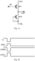
- an inverter for inversion of a low potential to a high potential, an inverter is proposed in the prior art, which is structured as illustrated in Fig. 1a .
- the inverter comprises two P-type TFT, wherein the first TFT has its gate connected with an input terminal IN, has its source connected with a high voltage signal (VGH) and has its drain connected with an output terminal (OUT).
- the second TFT has its gate and drain connected with a low voltage signal (VGL) and has its source connected with the output terminal OUT.
- Fig. 1b is a timing control diagram of the circuit illustrated in Fig. 1a . With reference to Fig. 1a and Fig.
- the first TFT is switched off when IN is at a high potential, and since the second TFT is diode connected, (the second TFT has both its gate and its drain connected with the low voltage signal VGL as mentioned above), a low potential which is higher than VGL by Vth is output by the output terminal OUT and when IN is at a low potential, both the first TFT and the second TFT are switched on, so a high potential is output by the output terminal OUT.
- the output terminal OUT is connected with both VGH and VGL, and if the TFTs are switched on or off completely, then the output terminal OUT should be connected either with VGH or with VGL, and thus the voltage output by the output terminal should be either VGH as a high voltage or VGL as a low voltage.
- the forgoing circuit suffers from the problem of both the two TFTs being switched on at the same time, and the voltage output by the output terminal OUT is at a potential between the high voltage and the low voltage due to voltage division.As a result, the high or low potential at which the voltage is output lies between the high voltage and low voltage, thus making the high or low potential output insufficient, resulting in a continuous power supply and increasing power consumption.
- the output potential is not sufficient (for example, an input voltage of-5V ⁇ 10V may generate an output voltage of -4.43V ⁇ 5.07V), failing to effectively control TFTs in a pixel, thus making the compensation circuit fail to operate effectively.
- the inverter includes first, second, third, and fourth transistors, where each of the first, second, third, and fourth transistors is a P-type thin film transistor, and a first capacitor.
- a gate of the first transistor is connected with a gate of the third transistor, and the gate of the first transistor and the gate of the third transistor are connected to an input terminal of a first signal.
- a source of the first transistor is connected with a source of the third transistor, and the source of the first transistor and the source of the third transistor are connected to an input terminal of a second signal.
- a drain of the first transistor is connected with a gate of the fourth transistor and a source of the second transistor at a first node, where a gate of the second transistor is connected with an input terminal of a second clock signal, a drain of the second transistor is connected with a drain of the fourth transistor, and the drain of the second transistor and the drain of the fourth transistor are connected to an input terminal of a third signal.
- a drain of the third transistor is connected with a source of the fourth transistor, and the drain of the third transistor and the source of the fourth transistor are connected to a signal output terminal of the inverter.
- the first capacitor has one terminal connected with the first node and has another terminal connected with an input terminal of a first clock signal, and where a high voltage signal is input to the input terminal of the second signal, and a low voltage signal is input to the input terminal of the third signal.
- a high potential is input to the input terminal of the first signal and a low potential is input to the input terminal of the first clock signal, and wherein at this period of time the signals to both terminals of the first capacitor do not simultaneously change so that the voltage of the input terminal of the third signal can be output completely by the signal output terminal of the inverter.
- the circuit includes an inverter.
- the inverter includes first, second, third, and fourth transistors, where each of the first, second, third, and fourth transistors is a P-type thin film transistor, and a first capacitor.
- a gate of the first transistor is connected with a gate of the third transistor, and the gate of the first transistor and the gate of the third transistor are connected to an input terminal of a first signal.
- a source of the first transistor is connected with a source of the third transistor, and the source of the first transistor and the source of the third transistor are connected to an input terminal of a second signal.
- a drain of the first transistor is connected with a gate of the fourth transistor and a source of the second transistor at a first node, where a gate of the second transistor is connected with an input terminal of a second clock signal, a drain of the second transistor is connected with a drain of the fourth transistor, and the drain of the second transistor and the drain of the fourth transistor are connected to an input terminal of a third signal.
- a drain of the third transistor is connected with a source of the fourth transistor, and the drain of the third transistor and the source of the fourth transistor are connected to a signal output terminal of the inverter.
- the first capacitor has one terminal connected with the first node and has another terminal connected with an input terminal of a first clock signal, and where a high voltage signal is input to the input terminal of the second signal, and a low voltage signal is input to the input terminal of the third signal.
- the compensation circuit includes an inverter.
- the inverter includes first, second, third, and fourth transistors, where each of the first, second, third, and fourth transistors is a P-type thin film transistor, and a first capacitor.
- a gate of the first transistor is connected with a gate of the third transistor, and the gate of the first transistor and the gate of the third transistor are connected to an input terminal of a first signal.
- a source of the first transistor is connected with a source of the third transistor, and the source of the first transistor and the source of the third transistor are connected to an input terminal of a second signal.
- a drain of the first transistor is connected with a gate of the fourth transistor and a source of the second transistor at a first node, where a gate of the second transistor is connected with an input terminal of a second clock signal, a drain of the second transistor is connected with a drain of the fourth transistor, and the drain of the second transistor and the drain of the fourth transistor are connected to an input terminal of a third signal.
- a drain of the third transistor is connected with a source of the fourth transistor, and the drain of the third transistor and the source of the fourth transistor are connected to a signal output terminal of the inverter.
- the first capacitor has one terminal connected with the first node and has another terminal connected with an input terminal of a first clock signal, and where a high voltage signal is input to the input terminal of the second signal, and a low voltage signal is input to the input terminal of the third signal.
- an inverter includes an input inverter having a high-resistance load and a first transistor and an output buffer including second and third transistor coupled in series.
- a power supply voltage is provided to satisfy an inequality VDD1>VDD2+Vth where VDD1 is the power supply voltage of the input inverter, VDD2 is the power supply voltage of the output buffer, and Vth is the threshold voltage of the transistors.
- VDD1 is the power supply voltage of the input inverter
- VDD2 is the power supply voltage of the output buffer
- Vth is the threshold voltage of the transistors.
- embodiments of the invention provide an inverter, an AMOLED compensation circuit and a display panel.
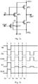
- Fig.2a is schematic structural diagram of a first inverter in an embodiment of the invention.
- the first inverter comprises a first transistor MP 1, a second transistor MP2, a third transistor MP3, a fourth transistor MP4 and a first capacitor C1.
- a gate of the first transistor MP1 is connected with a gate of the third transistor MP3, and the gate of the first transistor MP1 and the gate of the third transistor MP3 have a common terminal which is used as an input terminal of a first signal IN.
- a source of the first transistor MP1 is connected with a source of the third transistor MP3, and the source of the first transistor MP1 and the source of the third transistor MP3 are used as an input terminal VGH of a second signal.
- a drain of the first transistor MP1 is connected with a gate of the fourth transistor MP4 and a source of the second transistor MP2 at a first node N1, wherein, a high voltage signal is input to the input terminal VGH of the second signal.
- a gate of the second transistor MP2 is connected with an input terminal of a second clock signal input, a drain of the second transistor MP2 is connected a the drain of the fourth transistor MP4, and the drain of the second transistor MP2 and the drain of the fourth transistor MP4 have a common terminal which is used as an input terminal VGL of a third signal, wherein a low voltage signal is input to the input terminal VGL of the third signal.
- a drain of the third transistor MP3 is connected with a source of the fourth transistor MP4, and the drain of the third transistor MP3 and the source of the fourth transistor MP4 have a common terminal which is used as a signal output terminal OUT of the inverter.
- the first capacitor C1 has one terminal connected with the first node N1 and has the other terminal with an input terminal CK of a first clock signal.
- Fig.2b is a schematic timing control diagram of the inverter circuit in Fig.2a .
- a high potential is input to the input terminal IN of the first signal and the input terminal CK of the first clock signal, and a low potential is input to an input terminal CKB of a second clock signal, then the first transistor MP1 and the third transistor MP3 are switched off, and the second transistor MP2 and the fourth transistor MP4 are switched on. Since the second transistor MP2 is switched on, the first node N1 is connected to the input terminal VGL of the third signal, and also since the fourth transistor MP4 is switched on and the third transistor MP3 is switched off, a low potential is output to the signal output terminal OUT.
- a low potential is input to the input terminal IN of the first signal and the input terminal CK of the first clock signal, and a high potential is input to the input terminal CKB of the second clock signal, then the first transistor MP1 and the third transistor MP3 are switched on, and the second transistor MP2 and the fourth transistor MP4 are switched off.
- the first transistor MP1 since the first transistor MP1 is switched on, the first node N1 is connected to the input terminal VGH of the second signal, and also since the third transistor MP3 is switched on, a high potential is output to the signal output terminal OUT.
- a high potential is input to the input terminal IN of the first signal and the input terminal CK of the first clock signal, and a low potential is input to the input terminal CKB of the second clock signal, then the first transistor MP1 and the third transistor MP3 are switched off, and the second transistor MP2 and the fourth transistor MP4 are switched on.
- the first node N1 is connected to the input terminal VGL of the third signal, and also since the fourth transistor MP4 is switched on and the third transistor MP3 is switched off, a low potential is output to the signal output terminal OUT;
- a high potential is input to the input terminal IN of the first signal
- a low potential is input to the input terminal CK of the first clock signal
- a high potential is input to the input terminal CKB of the second clock signal
- the first transistor MP1 and the third transistor MP3 are switched off, and the second transistor MP2 is also switched off, therefore the first capacitor has no signal input to the upper terminal while its lower terminal is connected with the input terminal CK of the first clock signal.
- the signals to both terminals of the first capacitor will not simultaneously change, which otherwise results in a change in total amount of charge, so the first capacitor C1 meets the charge conservation law.
- the potential of the lower terminal of the first capacitor C1 drops, but the voltage between the two terminals of the first capacitor C1 will not change suddenly for the sake of charge conservation law. Therefore the potential of the upper terminal of the first capacitor is pulled down, in other words, the potential of the first node N1 is pulled down, which has the fourth transistor MP4 switched on, further causing a low potential being output to the signal output terminal OUT and having the signal output terminal OUT connected with VGL.
- the voltage of the VGL can be output completely by the signal output terminal OUT to thereby avoid the undesired phenomenon in the prior art of a potential failing to reach a preset voltage.
- a high potential is input to the input terminal IN of the first signal, and a high potential and a low potential are input alternatively to the input terminal CK of the first clock signal and to the input terminal CKB of the second clock signal, while maintaining all the time the upper terminal of the first capacitor being at a low potential ,that is, a low potential is always output to the signal output terminal OUT.
- a high potential is input to the input terminal IN of the first signal and the input terminal CK of the first clock signal, a low potential is input to the input terminal CKB of the second clock signal, and ultimately a low potential is output to the signal output terminal OUT, which is under the same operating principle as those during the first period of time T1 and the third period of time T3, and a repeated description thereof will be omitted here.
- a high potential is input to the input terminal IN of the first signal
- a low potential is input to the input terminal CK of the first clock signal
- a high potential is input to the input terminal CKB of the second clock signal
- a low potential is ultimately output to the signal output terminal OUT, which is under the same operating principle as those during the fourth period of time T4, and a repeated description thereof will be omitted here.
- the foregoing times T5 and T6 are repeated as subsequent times, and a repeated description thereof will be omitted here.
- both the first clock signal and the second clock signal serve to invert the first signal of the input terminal IN while controlling the output signal at a potential in a range of -5V ⁇ 10V to thereby ensure the output potential to meet a demand for pixel control.
- current in the input terminal VGH of a high voltage signal and current in the input terminal VGL of a low voltage signal will not be too high, thus reducing power consumption of the circuit.
- a second capacitor C2 is added in the second embodiment.
- One terminal of the second capacitor C2 is connected with the source of the third transistor MP3 and the other terminal is connected with the drain of the third transistor MP3 so that the problem of ripple of the output signal from the signal output terminal OUT due to the first clock signal from CK and the second clock signal from CKB is suppressed after the second period of time T2 to thereby make an output waveform from the signal output terminal OUT as smooth as possible.
- the inverters according to the first embodiment or the second embodiment can be applied to a compensation circuit of an Active Matrix Organic Light-Emitting Diode (AMOLED) display panel in combination with a general PMOS drive circuit, where an output signal is inverted as a drive signal of an EMIT drive circuit to thereby reduce power consumption of the circuit while ensuring an output potential to meet a demand for pixel control.
- AMOLED Active Matrix Organic Light-Emitting Diode
- a compensation circuit can be arranged in a display panel to compensate for a threshold voltage shift (Vth shift) due to the non-uniformity of TFTs manufactured in a panel production process and to overcome the shortcoming of a decline in stability of the TFTs due to a bias voltage caused by long-time switching on status of the TFTs.
- Vth shift threshold voltage shift
Landscapes
- Engineering & Computer Science (AREA)
- Physics & Mathematics (AREA)
- Computer Hardware Design (AREA)
- Computing Systems (AREA)
- General Engineering & Computer Science (AREA)
- Mathematical Physics (AREA)
- General Physics & Mathematics (AREA)
- Theoretical Computer Science (AREA)
- Control Of Indicators Other Than Cathode Ray Tubes (AREA)
- Control Of El Displays (AREA)
Claims (4)
- Wechselrichter, umfassend:erste, zweite, dritte und vierte Transistoren (MP1, MP2, MP3, MP4), wobei jeder der ersten, zweiten, dritten und vierten Transistoren (MP1, MP2, MP3, MP4) ein Dünnschichttransistor vom P-Typ ist; undeinen ersten Kondensator (C1),wobei ein Gate-Anschluss des ersten Transistors (MP1) mit einem Gate-Anschluss des dritten Transistors (MP3) verbunden ist und der Gate-Anschluss des ersten Transistors (MP1) und der Gate-Anschluss des dritten Transistors (MP3) mit einer Eingangsklemme für ein erstes Signal (IN) verbunden sind,
wobei ein Source-Anschluss des ersten Transistors (MP1) mit einem Source-Anschluss des dritten Transistors (MP3) verbunden ist und der Source-Anschluss des ersten Transistors (MP1) und der Source-Anschluss des dritten Transistors (MP3) mit einer Eingangsklemme für ein zweites Signal (VGH) verbunden sind,
wobei ein Drain-Anschluss des ersten Transistors (MP1) bei einem ersten Knoten (N1) mit einem Gate-Anschluss des vierten Transistors (MP4) und einem Source-Anschluss des zweiten Transistors (MP2) verbunden ist,
wobei ein Gate-Anschluss des zweiten Transistors (MP2) mit einer Eingangsklemme für ein zweites Taktsignal (CKB) verbunden ist, ein Drain-Anschluss des zweiten Transistors (MP2) mit einem Drain-Anschluss des vierten Transistors (MP4) verbunden ist und der Drain-Anschluss des zweiten Transistors (MP2) und der Drain-Anschluss des vierten Transistors (MP4) mit einer Eingangsklemme für ein drittes Signal (VGL) verbunden sind,
wobei ein Drain-Anschluss des dritten Transistors (MP3) mit einem Source-Anschluss des vierten Transistors (MP4) verbunden ist und der Drain-Anschluss des dritten Transistors (MP3) und der Source-Anschluss des vierten Transistors (MP4) mit einer Signalausgangsklemme des Wechselrichters (OUT) verbunden sind,
wobei der erste Kondensator (C1) eine Klemme aufweist, die mit dem ersten Knoten (N1) verbunden ist, und eine andere Klemme aufweist, die mit einer Eingangsklemme für ein erstes Taktsignal (CK) verbunden ist, und
wobei ein Hochspannungssignal in die Eingangsklemme für das zweite Signal (VGH) eingegeben wird und ein Niederspannungssignal in die Eingangsklemme für das dritte Signal (VGL) eingegeben wird,
dadurch gekennzeichnet, dass
das erste Taktsignal (CK) und das zweite Taktsignal (CKB) umgekehrt zueinander sind, wobei während eines Zeitraums (T4) ein hohes Potenzial in die Eingangsklemme (IN) für das erste Signal eingegeben wird und ein niedriges Potenzial in die Eingangsklemme (CK) für das erste Taktsignal eingegeben wird, und wobei sich während dieses Zeitraums (T4) die in beide Klemmen des ersten Kondensators (C1) eingegebenen Signale nicht gleichzeitig ändern, so dass die Spannung der Eingangsklemme für das dritte Signal (VGL) vollständig durch die Signalausgangsklemme des Wechselrichters (OUT) ausgegeben werden kann. - Wechselrichter nach Anspruch 1, ferner umfassend einen zweiten Kondensator (C2), von dem eine Klemme mit dem Source-Anschluss des dritten Transistors (MP3) verbunden ist und eine andere Klemme mit dem Drain-Anschluss des dritten Transistors (MP3) verbunden ist.
- Ausgleichsschaltung für eine Anzeigetafel mit organischen Aktivmatrix-Leuchtdioden, umfassend den Wechselrichter nach Anspruch 1 oder 2.
- Anzeigetafel, umfassend die Ausgleichsschaltung für eine Anzeigetafel mit organischen Aktivmatrix-Leuchtdioden nach Anspruch 3.
Applications Claiming Priority (1)
| Application Number | Priority Date | Filing Date | Title |
|---|---|---|---|
| CN201210476968.2A CN103268749B (zh) | 2012-11-21 | 2012-11-21 | 一种反相器、amoled补偿电路和显示面板 |
Publications (2)
| Publication Number | Publication Date |
|---|---|
| EP2736174A1 EP2736174A1 (de) | 2014-05-28 |
| EP2736174B1 true EP2736174B1 (de) | 2016-12-07 |
Family
ID=49012376
Family Applications (1)
| Application Number | Title | Priority Date | Filing Date |
|---|---|---|---|
| EP13190469.0A Active EP2736174B1 (de) | 2012-11-21 | 2013-10-28 | Wechselrichter, AMOLED-Ausgleichsschaltung und Anzeigetafel |
Country Status (3)
| Country | Link |
|---|---|
| US (1) | US9311849B2 (de) |
| EP (1) | EP2736174B1 (de) |
| CN (1) | CN103268749B (de) |
Families Citing this family (17)
| Publication number | Priority date | Publication date | Assignee | Title |
|---|---|---|---|---|
| CN104134425B (zh) | 2014-06-30 | 2017-02-01 | 上海天马有机发光显示技术有限公司 | 一种oled反相电路和显示面板 |
| CN104269137B (zh) | 2014-10-13 | 2016-08-24 | 上海天马有机发光显示技术有限公司 | 一种反相器、驱动电路和显示面板 |
| US9734751B2 (en) | 2014-10-13 | 2017-08-15 | Shanghai Tianma AM-OLED Co., Ltd. | Inverter, driving circuit and display panel |
| CN104517571B (zh) * | 2014-12-16 | 2017-06-16 | 上海天马有机发光显示技术有限公司 | 反相器及驱动电路、显示面板、显示装置 |
| CN104809979B (zh) | 2015-05-26 | 2017-07-18 | 京东方科技集团股份有限公司 | 一种反相器及驱动方法、goa单元、goa电路和显示装置 |
| CN104851385B (zh) * | 2015-06-08 | 2018-05-08 | 京东方科技集团股份有限公司 | 一种反相器、电压补偿电路和显示装置 |
| CN105096833B (zh) * | 2015-08-26 | 2017-06-06 | 京东方科技集团股份有限公司 | 生成发光控制信号的电路和方法以及像素电路驱动方法 |
| CN105047118B (zh) * | 2015-09-18 | 2018-11-23 | 京东方科技集团股份有限公司 | 反转电路及其驱动方法、触控显示面板和触控显示装置 |
| CN105405399B (zh) * | 2016-01-05 | 2019-07-05 | 京东方科技集团股份有限公司 | 一种像素电路、其驱动方法、显示面板及显示装置 |
| CN106452425A (zh) * | 2016-09-21 | 2017-02-22 | 宁波大学 | 一种p管采样型自举绝热电路及四级反相器/缓冲器 |
| CN106952614B (zh) * | 2017-03-20 | 2019-02-22 | 昆山国显光电有限公司 | 驱动电路、阵列基板、显示屏及其初始化方法 |
| CN106952602B (zh) * | 2017-04-14 | 2022-01-21 | 京东方科技集团股份有限公司 | 反相器模块、移位寄存器单元、阵列基板及显示装置 |
| CN107993615B (zh) * | 2017-12-06 | 2019-11-05 | 武汉华星光电半导体显示技术有限公司 | Goa电路单元、goa电路及显示面板 |
| EP3588780B1 (de) * | 2018-06-28 | 2021-03-03 | IMEC vzw | Logische schaltung mit niedrigem verbrauch |
| CN109584799A (zh) * | 2019-02-02 | 2019-04-05 | 京东方科技集团股份有限公司 | 一种像素驱动电路、像素电路、显示面板和显示装置 |
| CN111210766B (zh) * | 2020-02-24 | 2021-04-06 | 厦门天马微电子有限公司 | 反相器及其驱动方法、栅极驱动电路、显示装置 |
| KR20240024405A (ko) * | 2022-08-16 | 2024-02-26 | 삼성디스플레이 주식회사 | 게이트 드라이버 및 이를 포함하는 표시 장치 |
Family Cites Families (19)
| Publication number | Priority date | Publication date | Assignee | Title |
|---|---|---|---|---|
| US7327169B2 (en) * | 2002-09-25 | 2008-02-05 | Semiconductor Energy Laboratory Co., Ltd. | Clocked inverter, NAND, NOR and shift register |
| JP4425547B2 (ja) | 2003-01-17 | 2010-03-03 | 株式会社半導体エネルギー研究所 | パルス出力回路、シフトレジスタ、および電子機器 |
| JP3962953B2 (ja) * | 2003-12-26 | 2007-08-22 | カシオ計算機株式会社 | レベルシフト回路及び該レベルシフト回路を備えた信号出力回路 |
| KR100589324B1 (ko) * | 2004-05-11 | 2006-06-14 | 삼성에스디아이 주식회사 | 발광 표시 장치 및 그 구동 방법 |
| KR100624115B1 (ko) * | 2005-08-16 | 2006-09-15 | 삼성에스디아이 주식회사 | 유기전계발광장치의 발광제어 구동장치 |
| KR100666637B1 (ko) * | 2005-08-26 | 2007-01-10 | 삼성에스디아이 주식회사 | 유기 전계발광 표시장치의 발광제어 구동장치 |
| KR100646992B1 (ko) | 2005-09-13 | 2006-11-23 | 삼성에스디아이 주식회사 | 발광제어선 구동부 및 이를 이용한 유기 발광 표시장치 |
| KR100776511B1 (ko) * | 2006-04-18 | 2007-11-16 | 삼성에스디아이 주식회사 | 주사구동회로 및 이를 이용한 유기발광표시장치 |
| EP1895545B1 (de) * | 2006-08-31 | 2014-04-23 | Semiconductor Energy Laboratory Co., Ltd. | Flüssigkristallanzeigevorrichtung |
| JP4968671B2 (ja) * | 2006-11-27 | 2012-07-04 | Nltテクノロジー株式会社 | 半導体回路、走査回路、及びそれを用いた表示装置 |
| JP5057828B2 (ja) * | 2007-04-16 | 2012-10-24 | 株式会社ジャパンディスプレイイースト | 表示装置 |
| TWI371741B (en) * | 2007-12-12 | 2012-09-01 | Hannstar Display Corp | Driving signal generating circuit and signal generatiing method thereof |
| KR100911982B1 (ko) * | 2008-03-04 | 2009-08-13 | 삼성모바일디스플레이주식회사 | 이미션 구동부 및 이를 이용한 유기전계발광 표시장치 |
| EP2447950A1 (de) * | 2009-06-25 | 2012-05-02 | Sharp Kabushiki Kaisha | Schieberegisterschaltung, anzeigevorrichtung damit und verfahren zur ansteuerung der schieberegisterschaltung |
| CN102467890B (zh) * | 2010-10-29 | 2014-05-07 | 京东方科技集团股份有限公司 | 移位寄存器单元、栅极驱动装置及液晶显示器 |
| KR20120091880A (ko) * | 2011-02-10 | 2012-08-20 | 삼성디스플레이 주식회사 | 인버터 및 이를 이용한 유기전계발광 표시장치 |
| US8928647B2 (en) * | 2011-03-04 | 2015-01-06 | Sony Corporation | Inverter circuit and display unit |
| CN102708776B (zh) * | 2011-06-13 | 2014-12-24 | 京东方科技集团股份有限公司 | 移位寄存器、液晶显示器栅极驱动装置及液晶显示器 |
| KR101881853B1 (ko) * | 2012-02-29 | 2018-07-26 | 삼성디스플레이 주식회사 | 에미션 구동 유닛, 에미션 구동부 및 이를 포함하는 유기 발광 표시 장치 |
-
2012
- 2012-11-21 CN CN201210476968.2A patent/CN103268749B/zh active Active
-
2013
- 2013-10-24 US US14/062,726 patent/US9311849B2/en active Active
- 2013-10-28 EP EP13190469.0A patent/EP2736174B1/de active Active
Non-Patent Citations (1)
| Title |
|---|
| None * |
Also Published As
| Publication number | Publication date |
|---|---|
| US20140145919A1 (en) | 2014-05-29 |
| US9311849B2 (en) | 2016-04-12 |
| EP2736174A1 (de) | 2014-05-28 |
| CN103268749A (zh) | 2013-08-28 |
| CN103268749B (zh) | 2015-04-15 |
Similar Documents
| Publication | Publication Date | Title |
|---|---|---|
| US9311849B2 (en) | Inverter, AMOLED compensation circuit and display panel | |
| CN116580671B (zh) | 显示面板和显示装置 | |
| EP3142099B1 (de) | Kompensationspixelschaltung und anzeigevorrichtung | |
| US10770000B2 (en) | Pixel circuit, driving method, display panel and display device | |
| US10297195B2 (en) | Pixel circuit and driving method thereof, array substrate, display panel and display device | |
| US9734763B2 (en) | Pixel circuit, driving method and display apparatus | |
| US9779682B2 (en) | GOA circuit with forward-backward scan function | |
| US9972245B2 (en) | Pixel circuit, driving method for the pixel circuit, display panel, and display device | |
| US9847062B2 (en) | Scan driver and organic light-emitting display using same | |
| CN103198793B (zh) | 像素电路及其驱动方法、显示装置 | |
| US10515590B2 (en) | Pixel compensation circuit, driving method, display panel and display device | |
| EP3159879B1 (de) | Pixelschaltung und anzeigevorrichtung | |
| US20180226019A1 (en) | Pixel circuit and driving method, and display device | |
| US10235932B2 (en) | OLED inverting circuit and display panel | |
| WO2016173124A1 (zh) | 像素电路、其驱动方法及相关装置 | |
| KR20130132417A (ko) | 어레이 기판 행 구동 유닛, 어레이 기판 행 구동 회로 및 디스플레이 장치 | |
| EP3159878B1 (de) | Pixelschaltung und anzeigevorrichtung | |
| CN104658481B (zh) | 一种像素补偿电路、显示装置和驱动方法 | |
| US10140922B2 (en) | Pixel driving circuit and driving method thereof and display device | |
| CN104091820A (zh) | 像素电路和显示装置 | |
| US20190189077A1 (en) | Pixel driving circuit, array substrate and display device | |
| CN114005410B (zh) | 一种显示面板、其驱动方法及显示装置 | |
| US9805655B2 (en) | Pixel circuit and driving method thereof, display device | |
| CN203950535U (zh) | 像素电路和显示装置 | |
| KR20180078932A (ko) | 유기 발광 다이오드 표시 장치의 구동 방법 |
Legal Events
| Date | Code | Title | Description |
|---|---|---|---|
| PUAI | Public reference made under article 153(3) epc to a published international application that has entered the european phase |
Free format text: ORIGINAL CODE: 0009012 |
|
| 17P | Request for examination filed |
Effective date: 20131028 |
|
| AK | Designated contracting states |
Kind code of ref document: A1 Designated state(s): AL AT BE BG CH CY CZ DE DK EE ES FI FR GB GR HR HU IE IS IT LI LT LU LV MC MK MT NL NO PL PT RO RS SE SI SK SM TR |
|
| AX | Request for extension of the european patent |
Extension state: BA ME |
|
| R17P | Request for examination filed (corrected) |
Effective date: 20141120 |
|
| RBV | Designated contracting states (corrected) |
Designated state(s): AL AT BE BG CH CY CZ DE DK EE ES FI FR GB GR HR HU IE IS IT LI LT LU LV MC MK MT NL NO PL PT RO RS SE SI SK SM TR |
|
| GRAP | Despatch of communication of intention to grant a patent |
Free format text: ORIGINAL CODE: EPIDOSNIGR1 |
|
| INTG | Intention to grant announced |
Effective date: 20160830 |
|
| RIN1 | Information on inventor provided before grant (corrected) |
Inventor name: QIAN, DONG |
|
| GRAS | Grant fee paid |
Free format text: ORIGINAL CODE: EPIDOSNIGR3 |
|
| GRAA | (expected) grant |
Free format text: ORIGINAL CODE: 0009210 |
|
| AK | Designated contracting states |
Kind code of ref document: B1 Designated state(s): AL AT BE BG CH CY CZ DE DK EE ES FI FR GB GR HR HU IE IS IT LI LT LU LV MC MK MT NL NO PL PT RO RS SE SI SK SM TR |
|
| REG | Reference to a national code |
Ref country code: GB Ref legal event code: FG4D |
|
| REG | Reference to a national code |
Ref country code: CH Ref legal event code: EP Ref country code: AT Ref legal event code: REF Ref document number: 852503 Country of ref document: AT Kind code of ref document: T Effective date: 20161215 |
|
| REG | Reference to a national code |
Ref country code: IE Ref legal event code: FG4D |
|
| REG | Reference to a national code |
Ref country code: DE Ref legal event code: R096 Ref document number: 602013014975 Country of ref document: DE |
|
| PG25 | Lapsed in a contracting state [announced via postgrant information from national office to epo] |
Ref country code: LV Free format text: LAPSE BECAUSE OF FAILURE TO SUBMIT A TRANSLATION OF THE DESCRIPTION OR TO PAY THE FEE WITHIN THE PRESCRIBED TIME-LIMIT Effective date: 20161207 |
|
| REG | Reference to a national code |
Ref country code: LT Ref legal event code: MG4D |
|
| REG | Reference to a national code |
Ref country code: NL Ref legal event code: MP Effective date: 20161207 |
|
| PG25 | Lapsed in a contracting state [announced via postgrant information from national office to epo] |
Ref country code: NO Free format text: LAPSE BECAUSE OF FAILURE TO SUBMIT A TRANSLATION OF THE DESCRIPTION OR TO PAY THE FEE WITHIN THE PRESCRIBED TIME-LIMIT Effective date: 20170307 Ref country code: LT Free format text: LAPSE BECAUSE OF FAILURE TO SUBMIT A TRANSLATION OF THE DESCRIPTION OR TO PAY THE FEE WITHIN THE PRESCRIBED TIME-LIMIT Effective date: 20161207 Ref country code: SE Free format text: LAPSE BECAUSE OF FAILURE TO SUBMIT A TRANSLATION OF THE DESCRIPTION OR TO PAY THE FEE WITHIN THE PRESCRIBED TIME-LIMIT Effective date: 20161207 Ref country code: GR Free format text: LAPSE BECAUSE OF FAILURE TO SUBMIT A TRANSLATION OF THE DESCRIPTION OR TO PAY THE FEE WITHIN THE PRESCRIBED TIME-LIMIT Effective date: 20170308 |
|
| REG | Reference to a national code |
Ref country code: AT Ref legal event code: MK05 Ref document number: 852503 Country of ref document: AT Kind code of ref document: T Effective date: 20161207 |
|
| PG25 | Lapsed in a contracting state [announced via postgrant information from national office to epo] |
Ref country code: ES Free format text: LAPSE BECAUSE OF FAILURE TO SUBMIT A TRANSLATION OF THE DESCRIPTION OR TO PAY THE FEE WITHIN THE PRESCRIBED TIME-LIMIT Effective date: 20161207 Ref country code: HR Free format text: LAPSE BECAUSE OF FAILURE TO SUBMIT A TRANSLATION OF THE DESCRIPTION OR TO PAY THE FEE WITHIN THE PRESCRIBED TIME-LIMIT Effective date: 20161207 Ref country code: FI Free format text: LAPSE BECAUSE OF FAILURE TO SUBMIT A TRANSLATION OF THE DESCRIPTION OR TO PAY THE FEE WITHIN THE PRESCRIBED TIME-LIMIT Effective date: 20161207 Ref country code: RS Free format text: LAPSE BECAUSE OF FAILURE TO SUBMIT A TRANSLATION OF THE DESCRIPTION OR TO PAY THE FEE WITHIN THE PRESCRIBED TIME-LIMIT Effective date: 20161207 |
|
| PG25 | Lapsed in a contracting state [announced via postgrant information from national office to epo] |
Ref country code: NL Free format text: LAPSE BECAUSE OF FAILURE TO SUBMIT A TRANSLATION OF THE DESCRIPTION OR TO PAY THE FEE WITHIN THE PRESCRIBED TIME-LIMIT Effective date: 20161207 |
|
| PG25 | Lapsed in a contracting state [announced via postgrant information from national office to epo] |
Ref country code: EE Free format text: LAPSE BECAUSE OF FAILURE TO SUBMIT A TRANSLATION OF THE DESCRIPTION OR TO PAY THE FEE WITHIN THE PRESCRIBED TIME-LIMIT Effective date: 20161207 Ref country code: SK Free format text: LAPSE BECAUSE OF FAILURE TO SUBMIT A TRANSLATION OF THE DESCRIPTION OR TO PAY THE FEE WITHIN THE PRESCRIBED TIME-LIMIT Effective date: 20161207 Ref country code: CZ Free format text: LAPSE BECAUSE OF FAILURE TO SUBMIT A TRANSLATION OF THE DESCRIPTION OR TO PAY THE FEE WITHIN THE PRESCRIBED TIME-LIMIT Effective date: 20161207 Ref country code: RO Free format text: LAPSE BECAUSE OF FAILURE TO SUBMIT A TRANSLATION OF THE DESCRIPTION OR TO PAY THE FEE WITHIN THE PRESCRIBED TIME-LIMIT Effective date: 20161207 Ref country code: IS Free format text: LAPSE BECAUSE OF FAILURE TO SUBMIT A TRANSLATION OF THE DESCRIPTION OR TO PAY THE FEE WITHIN THE PRESCRIBED TIME-LIMIT Effective date: 20170407 |
|
| PG25 | Lapsed in a contracting state [announced via postgrant information from national office to epo] |
Ref country code: BG Free format text: LAPSE BECAUSE OF FAILURE TO SUBMIT A TRANSLATION OF THE DESCRIPTION OR TO PAY THE FEE WITHIN THE PRESCRIBED TIME-LIMIT Effective date: 20170307 Ref country code: BE Free format text: LAPSE BECAUSE OF FAILURE TO SUBMIT A TRANSLATION OF THE DESCRIPTION OR TO PAY THE FEE WITHIN THE PRESCRIBED TIME-LIMIT Effective date: 20161207 Ref country code: SM Free format text: LAPSE BECAUSE OF FAILURE TO SUBMIT A TRANSLATION OF THE DESCRIPTION OR TO PAY THE FEE WITHIN THE PRESCRIBED TIME-LIMIT Effective date: 20161207 Ref country code: PL Free format text: LAPSE BECAUSE OF FAILURE TO SUBMIT A TRANSLATION OF THE DESCRIPTION OR TO PAY THE FEE WITHIN THE PRESCRIBED TIME-LIMIT Effective date: 20161207 Ref country code: IT Free format text: LAPSE BECAUSE OF FAILURE TO SUBMIT A TRANSLATION OF THE DESCRIPTION OR TO PAY THE FEE WITHIN THE PRESCRIBED TIME-LIMIT Effective date: 20161207 Ref country code: AT Free format text: LAPSE BECAUSE OF FAILURE TO SUBMIT A TRANSLATION OF THE DESCRIPTION OR TO PAY THE FEE WITHIN THE PRESCRIBED TIME-LIMIT Effective date: 20161207 Ref country code: PT Free format text: LAPSE BECAUSE OF FAILURE TO SUBMIT A TRANSLATION OF THE DESCRIPTION OR TO PAY THE FEE WITHIN THE PRESCRIBED TIME-LIMIT Effective date: 20170407 |
|
| REG | Reference to a national code |
Ref country code: DE Ref legal event code: R097 Ref document number: 602013014975 Country of ref document: DE |
|
| PLBE | No opposition filed within time limit |
Free format text: ORIGINAL CODE: 0009261 |
|
| STAA | Information on the status of an ep patent application or granted ep patent |
Free format text: STATUS: NO OPPOSITION FILED WITHIN TIME LIMIT |
|
| 26N | No opposition filed |
Effective date: 20170908 |
|
| PG25 | Lapsed in a contracting state [announced via postgrant information from national office to epo] |
Ref country code: SI Free format text: LAPSE BECAUSE OF FAILURE TO SUBMIT A TRANSLATION OF THE DESCRIPTION OR TO PAY THE FEE WITHIN THE PRESCRIBED TIME-LIMIT Effective date: 20161207 Ref country code: DK Free format text: LAPSE BECAUSE OF FAILURE TO SUBMIT A TRANSLATION OF THE DESCRIPTION OR TO PAY THE FEE WITHIN THE PRESCRIBED TIME-LIMIT Effective date: 20161207 |
|
| PG25 | Lapsed in a contracting state [announced via postgrant information from national office to epo] |
Ref country code: MC Free format text: LAPSE BECAUSE OF FAILURE TO SUBMIT A TRANSLATION OF THE DESCRIPTION OR TO PAY THE FEE WITHIN THE PRESCRIBED TIME-LIMIT Effective date: 20161207 |
|
| REG | Reference to a national code |
Ref country code: CH Ref legal event code: PL |
|
| GBPC | Gb: european patent ceased through non-payment of renewal fee |
Effective date: 20171028 |
|
| REG | Reference to a national code |
Ref country code: IE Ref legal event code: MM4A |
|
| REG | Reference to a national code |
Ref country code: FR Ref legal event code: ST Effective date: 20180629 |
|
| PG25 | Lapsed in a contracting state [announced via postgrant information from national office to epo] |
Ref country code: GB Free format text: LAPSE BECAUSE OF NON-PAYMENT OF DUE FEES Effective date: 20171028 Ref country code: LI Free format text: LAPSE BECAUSE OF NON-PAYMENT OF DUE FEES Effective date: 20171031 Ref country code: CH Free format text: LAPSE BECAUSE OF NON-PAYMENT OF DUE FEES Effective date: 20171031 Ref country code: LU Free format text: LAPSE BECAUSE OF NON-PAYMENT OF DUE FEES Effective date: 20171028 |
|
| PG25 | Lapsed in a contracting state [announced via postgrant information from national office to epo] |
Ref country code: FR Free format text: LAPSE BECAUSE OF NON-PAYMENT OF DUE FEES Effective date: 20171031 |
|
| PG25 | Lapsed in a contracting state [announced via postgrant information from national office to epo] |
Ref country code: MT Free format text: LAPSE BECAUSE OF NON-PAYMENT OF DUE FEES Effective date: 20171028 |
|
| PG25 | Lapsed in a contracting state [announced via postgrant information from national office to epo] |
Ref country code: IE Free format text: LAPSE BECAUSE OF NON-PAYMENT OF DUE FEES Effective date: 20171028 |
|
| PG25 | Lapsed in a contracting state [announced via postgrant information from national office to epo] |
Ref country code: HU Free format text: LAPSE BECAUSE OF FAILURE TO SUBMIT A TRANSLATION OF THE DESCRIPTION OR TO PAY THE FEE WITHIN THE PRESCRIBED TIME-LIMIT; INVALID AB INITIO Effective date: 20131028 |
|
| PG25 | Lapsed in a contracting state [announced via postgrant information from national office to epo] |
Ref country code: CY Free format text: LAPSE BECAUSE OF NON-PAYMENT OF DUE FEES Effective date: 20161207 |
|
| PG25 | Lapsed in a contracting state [announced via postgrant information from national office to epo] |
Ref country code: MK Free format text: LAPSE BECAUSE OF FAILURE TO SUBMIT A TRANSLATION OF THE DESCRIPTION OR TO PAY THE FEE WITHIN THE PRESCRIBED TIME-LIMIT Effective date: 20161207 |
|
| PG25 | Lapsed in a contracting state [announced via postgrant information from national office to epo] |
Ref country code: TR Free format text: LAPSE BECAUSE OF FAILURE TO SUBMIT A TRANSLATION OF THE DESCRIPTION OR TO PAY THE FEE WITHIN THE PRESCRIBED TIME-LIMIT Effective date: 20161207 |
|
| PG25 | Lapsed in a contracting state [announced via postgrant information from national office to epo] |
Ref country code: AL Free format text: LAPSE BECAUSE OF FAILURE TO SUBMIT A TRANSLATION OF THE DESCRIPTION OR TO PAY THE FEE WITHIN THE PRESCRIBED TIME-LIMIT Effective date: 20161207 |
|
| PGFP | Annual fee paid to national office [announced via postgrant information from national office to epo] |
Ref country code: DE Payment date: 20251027 Year of fee payment: 13 |