EP2733753A1 - Light emitting module - Google Patents
Light emitting module Download PDFInfo
- Publication number
- EP2733753A1 EP2733753A1 EP12811949.2A EP12811949A EP2733753A1 EP 2733753 A1 EP2733753 A1 EP 2733753A1 EP 12811949 A EP12811949 A EP 12811949A EP 2733753 A1 EP2733753 A1 EP 2733753A1
- Authority
- EP
- European Patent Office
- Prior art keywords
- light emitting
- light
- luminescent material
- semiconductor light
- emitting element
- Prior art date
- Legal status (The legal status is an assumption and is not a legal conclusion. Google has not performed a legal analysis and makes no representation as to the accuracy of the status listed.)
- Granted
Links
Images


Classifications
-
- F—MECHANICAL ENGINEERING; LIGHTING; HEATING; WEAPONS; BLASTING
- F21—LIGHTING
- F21S—NON-PORTABLE LIGHTING DEVICES; SYSTEMS THEREOF; VEHICLE LIGHTING DEVICES SPECIALLY ADAPTED FOR VEHICLE EXTERIORS
- F21S41/00—Illuminating devices specially adapted for vehicle exteriors, e.g. headlamps
- F21S41/10—Illuminating devices specially adapted for vehicle exteriors, e.g. headlamps characterised by the light source
- F21S41/14—Illuminating devices specially adapted for vehicle exteriors, e.g. headlamps characterised by the light source characterised by the type of light source
- F21S41/141—Light emitting diodes [LED]
- F21S41/143—Light emitting diodes [LED] the main emission direction of the LED being parallel to the optical axis of the illuminating device
-
- F—MECHANICAL ENGINEERING; LIGHTING; HEATING; WEAPONS; BLASTING
- F21—LIGHTING
- F21S—NON-PORTABLE LIGHTING DEVICES; SYSTEMS THEREOF; VEHICLE LIGHTING DEVICES SPECIALLY ADAPTED FOR VEHICLE EXTERIORS
- F21S41/00—Illuminating devices specially adapted for vehicle exteriors, e.g. headlamps
- F21S41/10—Illuminating devices specially adapted for vehicle exteriors, e.g. headlamps characterised by the light source
- F21S41/14—Illuminating devices specially adapted for vehicle exteriors, e.g. headlamps characterised by the light source characterised by the type of light source
- F21S41/141—Light emitting diodes [LED]
- F21S41/151—Light emitting diodes [LED] arranged in one or more lines
-
- F—MECHANICAL ENGINEERING; LIGHTING; HEATING; WEAPONS; BLASTING
- F21—LIGHTING
- F21S—NON-PORTABLE LIGHTING DEVICES; SYSTEMS THEREOF; VEHICLE LIGHTING DEVICES SPECIALLY ADAPTED FOR VEHICLE EXTERIORS
- F21S41/00—Illuminating devices specially adapted for vehicle exteriors, e.g. headlamps
- F21S41/10—Illuminating devices specially adapted for vehicle exteriors, e.g. headlamps characterised by the light source
- F21S41/14—Illuminating devices specially adapted for vehicle exteriors, e.g. headlamps characterised by the light source characterised by the type of light source
- F21S41/141—Light emitting diodes [LED]
- F21S41/151—Light emitting diodes [LED] arranged in one or more lines
- F21S41/153—Light emitting diodes [LED] arranged in one or more lines arranged in a matrix
-
- F—MECHANICAL ENGINEERING; LIGHTING; HEATING; WEAPONS; BLASTING
- F21—LIGHTING
- F21S—NON-PORTABLE LIGHTING DEVICES; SYSTEMS THEREOF; VEHICLE LIGHTING DEVICES SPECIALLY ADAPTED FOR VEHICLE EXTERIORS
- F21S41/00—Illuminating devices specially adapted for vehicle exteriors, e.g. headlamps
- F21S41/10—Illuminating devices specially adapted for vehicle exteriors, e.g. headlamps characterised by the light source
- F21S41/14—Illuminating devices specially adapted for vehicle exteriors, e.g. headlamps characterised by the light source characterised by the type of light source
- F21S41/176—Light sources where the light is generated by photoluminescent material spaced from a primary light generating element
-
- F—MECHANICAL ENGINEERING; LIGHTING; HEATING; WEAPONS; BLASTING
- F21—LIGHTING
- F21S—NON-PORTABLE LIGHTING DEVICES; SYSTEMS THEREOF; VEHICLE LIGHTING DEVICES SPECIALLY ADAPTED FOR VEHICLE EXTERIORS
- F21S41/00—Illuminating devices specially adapted for vehicle exteriors, e.g. headlamps
- F21S41/20—Illuminating devices specially adapted for vehicle exteriors, e.g. headlamps characterised by refractors, transparent cover plates, light guides or filters
- F21S41/24—Light guides
-
- F—MECHANICAL ENGINEERING; LIGHTING; HEATING; WEAPONS; BLASTING
- F21—LIGHTING
- F21S—NON-PORTABLE LIGHTING DEVICES; SYSTEMS THEREOF; VEHICLE LIGHTING DEVICES SPECIALLY ADAPTED FOR VEHICLE EXTERIORS
- F21S41/00—Illuminating devices specially adapted for vehicle exteriors, e.g. headlamps
- F21S41/20—Illuminating devices specially adapted for vehicle exteriors, e.g. headlamps characterised by refractors, transparent cover plates, light guides or filters
- F21S41/285—Refractors, transparent cover plates, light guides or filters not provided in groups F21S41/24 - F21S41/2805
-
- F—MECHANICAL ENGINEERING; LIGHTING; HEATING; WEAPONS; BLASTING
- F21—LIGHTING
- F21S—NON-PORTABLE LIGHTING DEVICES; SYSTEMS THEREOF; VEHICLE LIGHTING DEVICES SPECIALLY ADAPTED FOR VEHICLE EXTERIORS
- F21S41/00—Illuminating devices specially adapted for vehicle exteriors, e.g. headlamps
- F21S41/30—Illuminating devices specially adapted for vehicle exteriors, e.g. headlamps characterised by reflectors
- F21S41/32—Optical layout thereof
-
- F—MECHANICAL ENGINEERING; LIGHTING; HEATING; WEAPONS; BLASTING
- F21—LIGHTING
- F21S—NON-PORTABLE LIGHTING DEVICES; SYSTEMS THEREOF; VEHICLE LIGHTING DEVICES SPECIALLY ADAPTED FOR VEHICLE EXTERIORS
- F21S41/00—Illuminating devices specially adapted for vehicle exteriors, e.g. headlamps
- F21S41/30—Illuminating devices specially adapted for vehicle exteriors, e.g. headlamps characterised by reflectors
- F21S41/32—Optical layout thereof
- F21S41/321—Optical layout thereof the reflector being a surface of revolution or a planar surface, e.g. truncated
-
- F—MECHANICAL ENGINEERING; LIGHTING; HEATING; WEAPONS; BLASTING
- F21—LIGHTING
- F21S—NON-PORTABLE LIGHTING DEVICES; SYSTEMS THEREOF; VEHICLE LIGHTING DEVICES SPECIALLY ADAPTED FOR VEHICLE EXTERIORS
- F21S41/00—Illuminating devices specially adapted for vehicle exteriors, e.g. headlamps
- F21S41/30—Illuminating devices specially adapted for vehicle exteriors, e.g. headlamps characterised by reflectors
- F21S41/32—Optical layout thereof
- F21S41/322—Optical layout thereof the reflector using total internal reflection
-
- F—MECHANICAL ENGINEERING; LIGHTING; HEATING; WEAPONS; BLASTING
- F21—LIGHTING
- F21S—NON-PORTABLE LIGHTING DEVICES; SYSTEMS THEREOF; VEHICLE LIGHTING DEVICES SPECIALLY ADAPTED FOR VEHICLE EXTERIORS
- F21S45/00—Arrangements within vehicle lighting devices specially adapted for vehicle exteriors, for purposes other than emission or distribution of light
- F21S45/40—Cooling of lighting devices
- F21S45/42—Forced cooling
- F21S45/43—Forced cooling using gas
-
- H—ELECTRICITY
- H10—SEMICONDUCTOR DEVICES; ELECTRIC SOLID-STATE DEVICES NOT OTHERWISE PROVIDED FOR
- H10H—INORGANIC LIGHT-EMITTING SEMICONDUCTOR DEVICES HAVING POTENTIAL BARRIERS
- H10H20/00—Individual inorganic light-emitting semiconductor devices having potential barriers, e.g. light-emitting diodes [LED]
- H10H20/01—Manufacture or treatment
- H10H20/036—Manufacture or treatment of packages
- H10H20/0363—Manufacture or treatment of packages of optical field-shaping means
-
- H—ELECTRICITY
- H10—SEMICONDUCTOR DEVICES; ELECTRIC SOLID-STATE DEVICES NOT OTHERWISE PROVIDED FOR
- H10H—INORGANIC LIGHT-EMITTING SEMICONDUCTOR DEVICES HAVING POTENTIAL BARRIERS
- H10H20/00—Individual inorganic light-emitting semiconductor devices having potential barriers, e.g. light-emitting diodes [LED]
- H10H20/80—Constructional details
- H10H20/84—Coatings, e.g. passivation layers or antireflective coatings
-
- H—ELECTRICITY
- H10—SEMICONDUCTOR DEVICES; ELECTRIC SOLID-STATE DEVICES NOT OTHERWISE PROVIDED FOR
- H10H—INORGANIC LIGHT-EMITTING SEMICONDUCTOR DEVICES HAVING POTENTIAL BARRIERS
- H10H20/00—Individual inorganic light-emitting semiconductor devices having potential barriers, e.g. light-emitting diodes [LED]
- H10H20/80—Constructional details
- H10H20/85—Packages
- H10H20/851—Wavelength conversion means
- H10H20/8515—Wavelength conversion means not being in contact with the bodies
-
- H—ELECTRICITY
- H10—SEMICONDUCTOR DEVICES; ELECTRIC SOLID-STATE DEVICES NOT OTHERWISE PROVIDED FOR
- H10H—INORGANIC LIGHT-EMITTING SEMICONDUCTOR DEVICES HAVING POTENTIAL BARRIERS
- H10H20/00—Individual inorganic light-emitting semiconductor devices having potential barriers, e.g. light-emitting diodes [LED]
- H10H20/80—Constructional details
- H10H20/85—Packages
- H10H20/852—Encapsulations
-
- H—ELECTRICITY
- H10—SEMICONDUCTOR DEVICES; ELECTRIC SOLID-STATE DEVICES NOT OTHERWISE PROVIDED FOR
- H10H—INORGANIC LIGHT-EMITTING SEMICONDUCTOR DEVICES HAVING POTENTIAL BARRIERS
- H10H20/00—Individual inorganic light-emitting semiconductor devices having potential barriers, e.g. light-emitting diodes [LED]
- H10H20/80—Constructional details
- H10H20/85—Packages
- H10H20/852—Encapsulations
- H10H20/853—Encapsulations characterised by their shape
-
- H—ELECTRICITY
- H10—SEMICONDUCTOR DEVICES; ELECTRIC SOLID-STATE DEVICES NOT OTHERWISE PROVIDED FOR
- H10H—INORGANIC LIGHT-EMITTING SEMICONDUCTOR DEVICES HAVING POTENTIAL BARRIERS
- H10H20/00—Individual inorganic light-emitting semiconductor devices having potential barriers, e.g. light-emitting diodes [LED]
- H10H20/80—Constructional details
- H10H20/85—Packages
- H10H20/855—Optical field-shaping means, e.g. lenses
-
- H—ELECTRICITY
- H10—SEMICONDUCTOR DEVICES; ELECTRIC SOLID-STATE DEVICES NOT OTHERWISE PROVIDED FOR
- H10W—GENERIC PACKAGES, INTERCONNECTIONS, CONNECTORS OR OTHER CONSTRUCTIONAL DETAILS OF DEVICES COVERED BY CLASS H10
- H10W90/00—Package configurations
-
- F—MECHANICAL ENGINEERING; LIGHTING; HEATING; WEAPONS; BLASTING
- F21—LIGHTING
- F21S—NON-PORTABLE LIGHTING DEVICES; SYSTEMS THEREOF; VEHICLE LIGHTING DEVICES SPECIALLY ADAPTED FOR VEHICLE EXTERIORS
- F21S45/00—Arrangements within vehicle lighting devices specially adapted for vehicle exteriors, for purposes other than emission or distribution of light
- F21S45/40—Cooling of lighting devices
- F21S45/42—Forced cooling
- F21S45/43—Forced cooling using gas
- F21S45/435—Forced cooling using gas circulating the gas within a closed system
-
- H—ELECTRICITY
- H10—SEMICONDUCTOR DEVICES; ELECTRIC SOLID-STATE DEVICES NOT OTHERWISE PROVIDED FOR
- H10W—GENERIC PACKAGES, INTERCONNECTIONS, CONNECTORS OR OTHER CONSTRUCTIONAL DETAILS OF DEVICES COVERED BY CLASS H10
- H10W72/00—Interconnections or connectors in packages
- H10W72/071—Connecting or disconnecting
- H10W72/072—Connecting or disconnecting of bump connectors
- H10W72/07251—Connecting or disconnecting of bump connectors characterised by changes in properties of the bump connectors during connecting
-
- H—ELECTRICITY
- H10—SEMICONDUCTOR DEVICES; ELECTRIC SOLID-STATE DEVICES NOT OTHERWISE PROVIDED FOR
- H10W—GENERIC PACKAGES, INTERCONNECTIONS, CONNECTORS OR OTHER CONSTRUCTIONAL DETAILS OF DEVICES COVERED BY CLASS H10
- H10W72/00—Interconnections or connectors in packages
- H10W72/20—Bump connectors, e.g. solder bumps or copper pillars; Dummy bumps; Thermal bumps
Definitions
- the present invention relates to a light emitting module.
- the invention relates more particularly to a technical field in which a transparent resin is applied to distal end portions of light shielding walls which surround a semiconductor light emitting element from the circumference thereof to thereby form a clear cutoff line in a light distribution pattern.
- light emitting modules which employ a semiconductor light emitting element such as a light emitting diode (LED) as a light source, and these light emitting modules are equipped, for example, in vehicle lamps which shine light emitted from the semiconductor light emitting element as illumination light.
- a predetermined light distribution pattern is formed by light shone as illumination light.
- these light emitting modules there are some light emitting modules which has a plurality of semiconductor light emitting elements which shine light, a circuit board on which the semiconductor light emitting elements are mounted, luminescent material layers which change a wavelength of light emitted from the corresponding semiconductor light emitting elements, and light shielding walls which surround the semiconductor light emitting elements and the luminescent material layers from the circumference thereof (for example, refer to Patent Literature 1).
- Patent Literature 1 JP-A-2011-40495
- an external surface of the luminescent material layer does not have to project further forwards than distal ends of the light shielding walls in order to prevent the incidence of light emitted from each semiconductor light emitting element on the semiconductor light emitting elements which lie adjacent thereto.
- the distal end portions of the light shielding walls are designed so as to project further forwards than the external surface of the luminescent material layer with an allowance which takes the variances described above into consideration.
- part of the light emitted from the semiconductor emitting element and the luminescent material layer is reflected on the light shielding walls to thereby be shone as illumination light, part of which is then shone as direct illumination light.
- the quantity of light shone by the distal end portion of the light shielding wall which projects further forwards than the luminescent material layer becomes smaller than the quantity of light emitted from the other portions of the light shielding wall by such an extent that there is no light which is shone from the luminescent material layer as direct illumination light.
- Part of light which is reflected at the distal end portions of the light shielding walls constitutes light which forms a cutoff line.
- a problem to be solved by the invention is how to overcome the aforesaid problem, so as to form a clear cutoff line in a light distribution pattern.
- part of the light emitted from the semiconductor light emitting element is internally reflected in the transparent resin, and the light which is internally reflected in the transparent resin is reflected on the light shielding wall to thereby increase the quantity of light at the distal end portion of the light shielding wall. Therefore, the difference between the quantity of light shone from the distal end portion of the light shielding wall and the quantity of light shone from the other portions than the distal end portion of the light shielding wall is reduced, thereby making it possible to form a clear cutoff line in the light distribution pattern.
- the luminous intensity of the light distribution pattern formed by light emitted from the plurality of semiconductor light emitting elements can be made uniform, and a clear cutoff line can be formed.
- the transparent resin can be applied simultaneously in the step where the bonding resin is applied, and therefore, the light emitting module can easily be fabricated, and a reduction in the fabrication time of the light emitting module can be realized.
- a light emitting module of the invention is applied to a light emitting module which is provided in a vehicle headlamp. It is noted that the application of the light emitting module of the invention is not limited the light emitting module provided in the vehicle headlamp and hence that the invention can also widely be applied to other various types of vehicle lamps than the vehicle headlamp.
- a vehicle headlamp 1 is disposed mounted at each of left- and right-hand end portions of a front end portion of a vehicle body.
- the vehicle headlamp 1 includes a lamp housing 2 which is formed into a concave shape which is opened to the front and a cover 3 which closes an opening side of the lamp housing 2, and a lamp outer housing 4 is made up of the lamp housing 2 and the cover 3. An interior space of the lamp outer housing 4 is formed as a lamp compartment 5.
- a lamp unit 6 is disposed in the lamp compartment 5.
- the lamp unit 6 has a bracket 7, a light emitting module 8, a reflector 9, a lens holder 10 and a projection lens 11.
- the bracket 7 is formed, for example, of a metallic material having high thermal conductivity, and a front surface thereof is formed as a mounting surface 7a.
- Heat dissipating fins 7b, 7b, ... are provided on a rear surface of the bracket 7 so as to project to the rear.
- a fan 12 is attached to rear surfaces of the heat dissipating fins 7b, 7b, ... which are provided on the bracket 7. Heat generated when the light emitting module 8 is driven is dissipated by the heat dissipating fins 7b, 7b, ... and the fan 12.
- the light emitting module 8 has semiconductor light emitting elements 13, 13 which emit light, ..., a circuit board 14 on which the semiconductor light emitting elements 13, 13, ... are mounted, luminescent material layers 15, 15, ... which change a wavelength of at least part of light emitted from the semiconductor light emitting elements 13, 13, ... and light shielding walls 16, 16, ... which are provided on the circuit board 14.
- Front surfaces of the semiconductor light emitting elements 13, 13, ... are made into light emitting surfaces 13a, 13a, ... from which light is emitted, and rear surfaces thereof are made into surfaces on which the light emitting elements 13, 13, ... are mounted on the circuit board 14.
- the semiconductor light emitting elements 13, 13, ... are provided side by side at predetermined intervals in a left-to-right direction.
- a light emitting diode (LED) which emits light of a blue wavelength is used as the semiconductor light emitting elements 13, 13, ....
- the circuit board 14 is mounted on a central portion of the mounting surface 7a of the bracket 7 (refer to Fig. 1 ).
- the semiconductor light emitting elements 13, 13, ... are each connected to a circuit pattern, not shown, which is formed on the circuit board 14 via connecting terminals 17, 17, ....
- the semiconductor light emitting elements 13, 13, ... can be individually and separately illuminated to emit light by means of a driving voltage supplied from a power supply circuit, not shown.
- the luminescent material layers 15, 15, ... are formed, for example, of a material such as ceramic or glass and are disposed so as to cover the corresponding light emitting surfaces 13a, 13a, ... of the semiconductor light emitting elements 13, 13, ....
- the luminescent material layers 15 are each formed into a truncated quadrangular prism whose external form expands as they extend to the front, and external surfaces thereof are made up of a front surface 15a, a rear surface 15b and four side surfaces 15c, 15c, ... which are inclined so as to displaced outwards as they extend to the front.
- the rear surface 15b has substantially the same size of that of the light emitting surface 13a of the semiconductor light emitting element 13, and the front surface 15a is made larger than the rear surface 15b.
- a layer is used which has a yellow luminescent material which emits light of a yellow wavelength by being excited, for example, by light of a blue wavelength.
- blue light emitted from the semiconductor light emitting elements 13, 13, ... and yellow light emitted from the luminescent material layers 15, 15, ... are mixed together to emit white light.
- the light shielding walls 16, 16, ... are individually caused to project to the front from the circuit board 14 and are provided so as to surround vertically and horizontally the corresponding semiconductor light emitting elements 13, 13, ... and luminescent material layers 15, 15, ....
- the light shielding walls 16, 16, ... are each formed, for example, into a pentagonal prism which extends horizontally or vertically.
- the light shielding walls 16 are each made up of an erected portion 18 which connects to a front surface of the circuit board 14 and which is directed vertically or horizontally and an inclined portion 19 which is inclined so that both surfaces (external surfaces) thereof approach each other as the inclined portion 19 extends to the front from a front end of the erected portion 18.
- the external surfaces of the inclined portion 19 are formed as inclined surfaces 20, 20, and a front end of a distal end portion (a front end portion) 21 is made into an apex portion 21a.
- the inclined surfaces 20, 20 are inclined individually at an angle at which the inclined surfaces 20, 20 follow individually the side surfaces 15c, 15c of the luminescent material layers 15, 15.
- Outer circumferential surfaces of the light shielding walls 16, 16, ... which do not surround the semiconductor light emitting elements 13, 13, ... and the luminescent material layers 15, 15, ... may be directed vertically and horizontally without having an inclined surface as shown in Fig. 2 .
- the semiconductor light emitting element 13 is surrounded by the erected portions 18, 18, ... of the four light shielding walls 16, 16, ... from the circumference thereof, and the luminescent material layer 15 is surrounded by the inclined portions 19, 19, ... of the four light shielding walls 16, 16, ... from the circumference thereof.
- the four side surfaces 15c, 15c, ... of the luminescent material layer 15 and the four inclined surfaces 20, 20 which surround the luminescent material layer 15 from the circumference thereof individually stand opposite to each other.
- the distal end portions 21, 21, ... of the inclined portions 19, 19, ... are positioned further forwards than the front surface 15a of the luminescent material layer 15.
- the inclined surfaces 20, 20 ... external surfaces of the distal end portions 21, 21, ... are made into exposed surfaces 20a, 20a, ... while of the inclined surfaces 20, 20, other surfaces than the distal end portions 21, 21, ... are made into surrounding surfaces 20b, 20b, .... Consequently, the luminescent material layer 15 is surrounded from the circumference thereof by the four surrounding surfaces 20b,
- portions which are each surrounded by the four distal end portions 21, 21, ... are formed as opening portions 22, 22, ... which are positioned at front sides of the luminescent material layers 15, 15, ....
- the rear surface 15b is bonded to the light emitting surface 13a of the semiconductor light emitting element 13 with a bonding resin 23, and the four side surfaces 15c, 15c, ... are bonded individually to the four surrounding surfaces 20b, 20b, ... of the light shielding walls 16, 16, ... with the bonding resin 23.
- the thickness of the bonding resin 23 applied between the luminescent material layer 15 and the semiconductor light emitting element 13 and the thickness of the bonding resin 23 applied between the luminescent material layer 15 and the light shielding walls 16, 16, ... are substantially uniform and the bonding resin 23 applied thin therebetween. Consequently, the side surfaces 15c, 15c, ... of the luminescent material layer 15 and the surrounding surfaces 20b, 20b, ... of the light shielding walls 16, 16, ... are positioned close to each other.
- the bonding resin 23 has light transmittivity, and for example, a silicone-based material is used as the boding resin 23.
- a transparent resin 24 is applied to cover the front surface 15a of the luminescent material layer 15 and the exposed surfaces 20a, 20a, ... of the four light shielding walls 16, 16, .... Namely, the transparent resin 24 is applied to cover the whole of the opening portion 22.
- the transparent resin 24 is applied substantially uniform, and a front surface 24a thereof is positioned on the same plane as a plane formed by the apex portions 21a, 21a, ... of the four distal end portions 21, 21, ....
- the transparent resin 24 has light transmittivity, and for example, the same material as that of the bonding resin 23 is used as the transparent resin 24.
- the transparent resin 24 and the bonding resin 23 are described exemplarily as being made of the same material, the transparent resin and the bonding resin may be made of different materials, as long as the materials are resins having light transmittivity.
- the transparent resin may be made of the same material as that of the luminescent material layer 15. As this occurs, as described above, since the apex portions 21a, 21a, ... of the distal end portions 21, 21, ... of the light shielding walls 16, 16, ... are positioned on the same plane as the front surface of the transparent resin, light which is shone from the transparent resin made of the same material as that of the luminescent material 15 as direct illumination light exists at the distal end portions 21, 21, ....
- the reflector 9 is made up of an upper reflector 25 which is disposed at an upper side of the light emitting module 8 and a lower reflector 26 which is disposed at a lower side of the light emitting module 8 (refer to Fig. 1 ).
- the upper reflector 25 and the lower reflector 26 have a substantially downwardly oriented surface on a side facing the light emitting module 8 and a substantially upwardly oriented surface on a side facing the light emitting module 8, respectively, and these surfaces are formed as reflecting surfaces 25a, 26a.
- the reflector 9 has a function to reflect light emitted from the light emitting module 8 towards the projection lens 11.
- the lens holder 10 is mounted on the mounting surface 7a of the bracket 7 and is formed into a ring-like shape which penetrates substantially in the front-to-rear direction and is provided so as to cover the light emitting module 8.
- the projection lens 11 is mounted at a front end portion of the lens holder 10 and is held ahead of the light emitting module 8 by the lens holder 10.
- the projection lens 11 has a function to project light emitted from the light emitting module 8 to the front.
- the lamp unit 6 is supported in the lamp housing 2 so as to tilt freely by a light axis control mechanism 27.
- the light axis control mechanism 27 has aiming screws 28, 28 and a leveling actuator 29.
- the aiming screws 28, 28 (only one of which is shown in Fig. 1 ) are positioned so as to be spaced apart from each other in the left-to-right direction and each connect an upper end portion of the bracket 7 with an upper end portion of the lamp housing 2.
- the lamp unit 6 is tilted substantially vertically or substantially horizontally by the aiming screw 28 being rotated, whereby the aiming of the lamp unit 6 is controlled.
- the leveling actuator 29 connects a lower end portion of the bracket 7 with a lower end portion of the lamp housing 2.
- the lamp unit 6 is tilted substantially vertically by the leveling actuator 29 being driven, whereby the leveling of the lamp unit 6 is controlled.
- a driving voltage is applied individually and separately to the semiconductor light emitting elements 13, 13, ... of the light emitting module 8 from the power supply circuit, whereby light is emitted from the emitting surfaces 13a, 13a, ... of the predetermined semiconductor light emitting elements 13, 13, ... to which the driving voltage is applied.
- part of the light which is reflected internally on the front surface 24a is guided in the transparent resin 24 and is then reflected totally on the exposed surfaces 20a, 20a, ... of the light shielding walls 16, 16, ... to thereby be emitted to the front (an optical path L).
- Part of the light which is reflected on the exposed surfaces 20a, 20a, ... to be emitted to the front constitutes light which forms a cutoff line of a light distribution pattern.
- Light emitted from the light emitting module 8 is reflected by the reflector 9 to be directed towards the projection lens 11 or travels directly thereto without being reflected by the reflector 9 and is shone to the front by the projection lens 11 to form a desired light distribution pattern.
- the transparent resin 24 is applied to a front side of the luminescent material layer 15, and an internal reflection is produced on the front surface 24a of the transparent resin 24.
- the transparent resin 24 is described exemplarily as being applied to close the whole of the opening portion 22 which is formed by the distal end portions 21, 21, ... of the light shielding walls 16, 16, ..., the transparent resin 24 may be applied in such a way as to close part of the opening portion 22, as long as the light reflected internally therein is directed totally to the exposed surfaces 20a, 20a, ....
- the transparent resin 24 may be applied only to an outer circumferential portion of the opening portion 22 in such a way as to cover the exposed surfaces 20a, 20a, ... (refer to Fig. 4 ). Also, in the case of the transparent resin 24 being applied only to the outer circumferential portion of the opening portion 22, as in the case of the transparent resin 24 being applied in such a way as to cover the whole of the opening portion 22, since an internal reflection is generated on an external surface 24b of the transparent resin 24, part of light is totally reflected by the exposed surfaces 20a, 20a, ... to thereby be emitted to the front. Consequently, the quantity of light which is shone at the distal end portions 21, 21, ... of the light shielding walls 16, 16, ... is increased, whereby the difference between the quantity of light shone at the distal end portions 21, 21, ... and the quantity of light shone at the other portions than the distal end portions 21, 21, ... is reduced.
- the transparent resin 24 When the transparent resin 24 is applied only to the outer circumferential portion of the opening portion 22, the evenness in quantity of light between light shone at the distal end portions 21, 21, ... and light shone at the other portions than the distal end portions 21, 21, ... can be ensured while reducing the amount of transparent resin 24 used to reduce, in turn, the production costs.
- the light emitting module 8 may be configured so that one semiconductor light emitting element 13 and one luminescent material layer 15 are surrounded from the circumference thereof by a plurality of light shielding walls 16, 16, ....
- part of light which is emitted from the semiconductor light emitting element 13 and which is reflected internally on the front surface 24a or the external surface 24b of the transparent resin 24 is reflected on the exposed surfaces 20a, 20a, ... of the light shielding walls 16, 16, ... to be shone to the front for formation of a light distribution pattern.
- the light shielding walls 16, 16, ... are provided so as to surround individually the plurality of semiconductor light emitting elements 13, 13, ... and the plurality of luminescent material layers 15, 15, ... from the circumference thereof.
- the transparent resin 24 is applied so as to close the whole of the opening portion 22 formed by the distal end portions 21, 21, ... of the light shielding walls 16, 16, ....
- the area in the transparent resin 24 where light is internally reflected is increased and part of light which is reflected internally on the front surface 24a of the transparent resin 24 is directed to the exposed surfaces 20a, 20a, ....
- the transparent resin 24 and the bonding resin 23 are made of the same material.
- the transparent resin 24 can be applied simultaneously in the step of applying the bonding resin 23, not only can the light emitting module 8 be fabricated easily, but also the fabrication time of the light emitting module 8 can be reduced.
- 8 light emitting module 13 semiconductor light emitting element; 13a light emitting surface; 14 circuit board; 15 luminescent material layer; 16 light shielding wall; 20a exposed surface; 21 distal end portion; 22 opening portion; 23 bonding resin; 24 transparent resin.
Landscapes
- Engineering & Computer Science (AREA)
- General Engineering & Computer Science (AREA)
- Physics & Mathematics (AREA)
- Microelectronics & Electronic Packaging (AREA)
- Optics & Photonics (AREA)
- Mathematical Physics (AREA)
- Led Device Packages (AREA)
- Non-Portable Lighting Devices Or Systems Thereof (AREA)
- Fastening Of Light Sources Or Lamp Holders (AREA)
Abstract
Description
- The present invention relates to a light emitting module. The invention relates more particularly to a technical field in which a transparent resin is applied to distal end portions of light shielding walls which surround a semiconductor light emitting element from the circumference thereof to thereby form a clear cutoff line in a light distribution pattern.
- There are light emitting modules which employ a semiconductor light emitting element such as a light emitting diode (LED) as a light source, and these light emitting modules are equipped, for example, in vehicle lamps which shine light emitted from the semiconductor light emitting element as illumination light. In these vehicle lamps, a predetermined light distribution pattern is formed by light shone as illumination light.
- In these light emitting modules, there are some light emitting modules which has a plurality of semiconductor light emitting elements which shine light, a circuit board on which the semiconductor light emitting elements are mounted, luminescent material layers which change a wavelength of light emitted from the corresponding semiconductor light emitting elements, and light shielding walls which surround the semiconductor light emitting elements and the luminescent material layers from the circumference thereof (for example, refer to Patent Literature 1).
- In a light emitting module described in Patent Literature 1, light emitted from each semiconductor light emitting element is prevented from being incident on the semiconductor light emitting elements which lie adjacent thereto by the light shielding walls which surround the semiconductor light emitting element and the luminescent material layer from the circumference thereof.
- Patent Literature 1:
JP-A-2011-40495 - Incidentally, an external surface of the luminescent material layer does not have to project further forwards than distal ends of the light shielding walls in order to prevent the incidence of light emitted from each semiconductor light emitting element on the semiconductor light emitting elements which lie adjacent thereto. However, there exists a possibility that there are caused variances in height of each light shielding wall, thickness of each semiconductor light emitting element and thickness of the adhesive due to machining or working accuracy in the production process of the light emitting module. Consequently, in order to prevent the projection of the external surface of the luminescent material layer from the distal ends of the light shielding walls, the distal end portions of the light shielding walls are designed so as to project further forwards than the external surface of the luminescent material layer with an allowance which takes the variances described above into consideration.
- In the light emitting module, part of the light emitted from the semiconductor emitting element and the luminescent material layer is reflected on the light shielding walls to thereby be shone as illumination light, part of which is then shone as direct illumination light. As this occurs, the quantity of light shone by the distal end portion of the light shielding wall which projects further forwards than the luminescent material layer becomes smaller than the quantity of light emitted from the other portions of the light shielding wall by such an extent that there is no light which is shone from the luminescent material layer as direct illumination light. Part of light which is reflected at the distal end portions of the light shielding walls constitutes light which forms a cutoff line.
- In the light emitting module described in Patent Literature 1, as described above, since the quality of light shone after having been reflected at the distal end portion of the light shielding wall is smaller than the quantity of light which is shone from the other portions than the distal end portion of the light shielding wall, the cutoff line in the light distribution pattern becomes unclear, leading to a problem that a desired light distribution pattern cannot be formed.
- Then, a problem to be solved by the invention is how to overcome the aforesaid problem, so as to form a clear cutoff line in a light distribution pattern.
-
- (1) With a view to solving the problem, according to the invention, there is provided a light emitting module characterized by including a semiconductor light emitting element which has a light emitting surface from which light is emitted, a circuit board on which the semiconductor light emitting element is mounted, a luminescent material layer which is disposed so as to cover the emitting surface of the semiconductor light emitting element and which changes a wavelength of at least part of light emitted from the semiconductor light emitting element and a light shielding wall which is provided on the circuit board and which surrounds the semiconductor light emitting element and the luminescent material layer from the circumference thereof, and characterized in that the luminescent material layer is bonded to the semiconductor light emitting element and the light shielding wall with a bonding resin having a light transmittivity, in that a distal end portion of the light shielding wall is caused to project further forwards than the luminescent material layer, and in that a transparent resin having a light transmittivity is applied so as to cover at least an exposed surface of the distal end portion of the light shielding wall.
- (2) In the invention described under (1) above, a plurality of semiconductor light emitting elements like the semiconductor light emitting element are mounted side by side at predetermined intervals, the same number of luminescent material layers like the luminescent material layer as the plurality of semiconductor light emitting elements are disposed so as to cover individually light emitting surfaces of the semiconductor light emitting elements, and the light shielding wall is provided so as to surround the plurality of semiconductor light emitting elements and the plurality of luminescent material layers from the circumference thereof.
- (3) In the invention described under (1) or (2) above, the transparent resin is applied so as to cover the whole of an opening portion which is formed by the distal end portion of the light shielding wall which is caused to project further forwards than the luminescent material layer.
- (4) In the invention described in any of (1) to (3) above, the transparent resin is made of the same material as that of the bonding resin.
- According to the invention described under (1) above, part of the light emitted from the semiconductor light emitting element is internally reflected in the transparent resin, and the light which is internally reflected in the transparent resin is reflected on the light shielding wall to thereby increase the quantity of light at the distal end portion of the light shielding wall. Therefore, the difference between the quantity of light shone from the distal end portion of the light shielding wall and the quantity of light shone from the other portions than the distal end portion of the light shielding wall is reduced, thereby making it possible to form a clear cutoff line in the light distribution pattern.
- According to the invention described under (2) above, the luminous intensity of the light distribution pattern formed by light emitted from the plurality of semiconductor light emitting elements can be made uniform, and a clear cutoff line can be formed.
- According to the invention described under (3) above, light which is internally reflected in the transparent resin to be reflected on the exposed surface of the light shielding wall is increased, and therefore, the quantity of light which is shone from the distal end portion of the light shielding wall and the quantity of light which is shone from the other portions than the distal end portion of the light shielding wall become even, thereby making it possible to form a far clearer cutoff line in the light distribution pattern.
- According to the invention described under (4) above, the transparent resin can be applied simultaneously in the step where the bonding resin is applied, and therefore, the light emitting module can easily be fabricated, and a reduction in the fabrication time of the light emitting module can be realized.
-
-
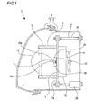
Fig. 1 shows an embodiment of the invention together withFigs. 2 to 4 and is a schematic vertical sectional view of a vehicle headlamp. -
Fig. 2 is an enlarged sectional view of a light emitting module. -
Fig. 3 is a conceptual drawing which shows an optical path of light emitted from a semiconductor light emitting element. -
Fig. 4 is an enlarged sectional view showing an example in which a transparent resin is applied to portions of an opening portion. - Hereinafter, referring to the accompanying drawings, a mode for carrying out a light emitting module of the invention will be described.
- In a form which will be described below, a light emitting module of the invention is applied to a light emitting module which is provided in a vehicle headlamp. It is noted that the application of the light emitting module of the invention is not limited the light emitting module provided in the vehicle headlamp and hence that the invention can also widely be applied to other various types of vehicle lamps than the vehicle headlamp.
- A vehicle headlamp 1 is disposed mounted at each of left- and right-hand end portions of a front end portion of a vehicle body.
- As shown in
Fig. 1 , the vehicle headlamp 1 includes alamp housing 2 which is formed into a concave shape which is opened to the front and acover 3 which closes an opening side of thelamp housing 2, and a lampouter housing 4 is made up of thelamp housing 2 and thecover 3. An interior space of the lampouter housing 4 is formed as alamp compartment 5. - A
lamp unit 6 is disposed in thelamp compartment 5. Thelamp unit 6 has abracket 7, alight emitting module 8, areflector 9, alens holder 10 and aprojection lens 11. - The
bracket 7 is formed, for example, of a metallic material having high thermal conductivity, and a front surface thereof is formed as amounting surface 7a.Heat dissipating fins Fig. 1 ) are provided on a rear surface of thebracket 7 so as to project to the rear. - A
fan 12 is attached to rear surfaces of theheat dissipating fins bracket 7. Heat generated when thelight emitting module 8 is driven is dissipated by theheat dissipating fins fan 12. - As shown in
Fig. 2 , thelight emitting module 8 has semiconductorlight emitting elements circuit board 14 on which the semiconductorlight emitting elements luminescent material layers light emitting elements light shielding walls circuit board 14. - Front surfaces of the semiconductor
light emitting elements light emitting surfaces light emitting elements circuit board 14. The semiconductorlight emitting elements light emitting elements - The
circuit board 14 is mounted on a central portion of themounting surface 7a of the bracket 7 (refer toFig. 1 ). - The semiconductor
light emitting elements circuit board 14 via connectingterminals light emitting elements - The
luminescent material layers light emitting surfaces light emitting elements luminescent material layers 15 are each formed into a truncated quadrangular prism whose external form expands as they extend to the front, and external surfaces thereof are made up of afront surface 15a, arear surface 15b and fourside surfaces rear surface 15b has substantially the same size of that of thelight emitting surface 13a of the semiconductorlight emitting element 13, and thefront surface 15a is made larger than therear surface 15b. As theluminescent material layers - In the
light emitting module 8, blue light emitted from the semiconductorlight emitting elements luminescent material layers - The
light shielding walls circuit board 14 and are provided so as to surround vertically and horizontally the corresponding semiconductorlight emitting elements luminescent material layers light shielding walls - The
light shielding walls 16 are each made up of anerected portion 18 which connects to a front surface of thecircuit board 14 and which is directed vertically or horizontally and aninclined portion 19 which is inclined so that both surfaces (external surfaces) thereof approach each other as theinclined portion 19 extends to the front from a front end of theerected portion 18. The external surfaces of theinclined portion 19 are formed asinclined surfaces apex portion 21a. Theinclined surfaces inclined surfaces side surfaces luminescent material layers - Outer circumferential surfaces of the
light shielding walls light emitting elements Fig. 2 . - The semiconductor
light emitting element 13 is surrounded by the erectedportions light shielding walls luminescent material layer 15 is surrounded by theinclined portions light shielding walls side surfaces luminescent material layer 15 and the fourinclined surfaces luminescent material layer 15 from the circumference thereof individually stand opposite to each other. Thedistal end portions inclined portions front surface 15a of theluminescent material layer 15. Of theinclined surfaces distal end portions surfaces inclined surfaces distal end portions surfaces luminescent material layer 15 is surrounded from the circumference thereof by the four surroundingsurfaces - In the
light emitting module 8, portions which are each surrounded by the fourdistal end portions portions - In the
luminescent material layer 15, therear surface 15b is bonded to thelight emitting surface 13a of the semiconductorlight emitting element 13 with abonding resin 23, and the fourside surfaces surfaces light shielding walls bonding resin 23. The thickness of thebonding resin 23 applied between theluminescent material layer 15 and the semiconductorlight emitting element 13 and the thickness of thebonding resin 23 applied between theluminescent material layer 15 and thelight shielding walls bonding resin 23 applied thin therebetween. Consequently, the side surfaces 15c, 15c, ... of theluminescent material layer 15 and the surroundingsurfaces light shielding walls - The
bonding resin 23 has light transmittivity, and for example, a silicone-based material is used as the bodingresin 23. - A
transparent resin 24 is applied to cover thefront surface 15a of theluminescent material layer 15 and the exposedsurfaces light shielding walls transparent resin 24 is applied to cover the whole of the openingportion 22. Thetransparent resin 24 is applied substantially uniform, and afront surface 24a thereof is positioned on the same plane as a plane formed by theapex portions distal end portions - The
transparent resin 24 has light transmittivity, and for example, the same material as that of thebonding resin 23 is used as thetransparent resin 24. - While the
transparent resin 24 and thebonding resin 23 are described exemplarily as being made of the same material, the transparent resin and the bonding resin may be made of different materials, as long as the materials are resins having light transmittivity. For example, the transparent resin may be made of the same material as that of theluminescent material layer 15. As this occurs, as described above, since theapex portions distal end portions light shielding walls luminescent material 15 as direct illumination light exists at thedistal end portions - The
reflector 9 is made up of anupper reflector 25 which is disposed at an upper side of thelight emitting module 8 and alower reflector 26 which is disposed at a lower side of the light emitting module 8 (refer toFig. 1 ). Theupper reflector 25 and thelower reflector 26 have a substantially downwardly oriented surface on a side facing thelight emitting module 8 and a substantially upwardly oriented surface on a side facing thelight emitting module 8, respectively, and these surfaces are formed as reflectingsurfaces reflector 9 has a function to reflect light emitted from thelight emitting module 8 towards theprojection lens 11. - The
lens holder 10 is mounted on the mountingsurface 7a of thebracket 7 and is formed into a ring-like shape which penetrates substantially in the front-to-rear direction and is provided so as to cover thelight emitting module 8. - The
projection lens 11 is mounted at a front end portion of thelens holder 10 and is held ahead of thelight emitting module 8 by thelens holder 10. Theprojection lens 11 has a function to project light emitted from thelight emitting module 8 to the front. - The
lamp unit 6 is supported in thelamp housing 2 so as to tilt freely by a lightaxis control mechanism 27. The lightaxis control mechanism 27 has aimingscrews actuator 29. - The aiming screws 28, 28 (only one of which is shown in
Fig. 1 ) are positioned so as to be spaced apart from each other in the left-to-right direction and each connect an upper end portion of thebracket 7 with an upper end portion of thelamp housing 2. Thelamp unit 6 is tilted substantially vertically or substantially horizontally by the aimingscrew 28 being rotated, whereby the aiming of thelamp unit 6 is controlled. - The leveling
actuator 29 connects a lower end portion of thebracket 7 with a lower end portion of thelamp housing 2. Thelamp unit 6 is tilted substantially vertically by the levelingactuator 29 being driven, whereby the leveling of thelamp unit 6 is controlled. - In the vehicle headlamp 1 which is configured as described above, a driving voltage is applied individually and separately to the semiconductor
light emitting elements light emitting module 8 from the power supply circuit, whereby light is emitted from the emittingsurfaces light emitting elements - When light is emitted from the semiconductor
light emitting elements transparent resins - In addition, when light is emitted from the semiconductor
light emitting elements bonding resin 23 and thereafter is reflected internally on thefront surface 15a of theluminescent material layer 15 or thefront surface 24a of thetransparent resin 24. Part of the light reflected internally on thefront surface 15a or thefront surface 24a is totally reflected on the surroundingsurfaces light shielding walls - In addition, part of the light which is reflected internally on the
front surface 24a is, as shown inFig. 3 , is guided in thetransparent resin 24 and is then reflected totally on the exposedsurfaces light shielding walls surfaces - Light emitted from the
light emitting module 8 is reflected by thereflector 9 to be directed towards theprojection lens 11 or travels directly thereto without being reflected by thereflector 9 and is shone to the front by theprojection lens 11 to form a desired light distribution pattern. - In the
light emitting module 8, as described above, thetransparent resin 24 is applied to a front side of theluminescent material layer 15, and an internal reflection is produced on thefront surface 24a of thetransparent resin 24. - Consequently, light which is emitted from the semiconductor
light emitting elements front surface 24a of thetransparent resin 24 is reflected on the exposedsurfaces light shielding walls distal end portions light shielding walls distal end portions distal end portions - In the description made above, while the
transparent resin 24 is described exemplarily as being applied to close the whole of the openingportion 22 which is formed by thedistal end portions light shielding walls transparent resin 24 may be applied in such a way as to close part of the openingportion 22, as long as the light reflected internally therein is directed totally to the exposedsurfaces - For example, the
transparent resin 24 may be applied only to an outer circumferential portion of the openingportion 22 in such a way as to cover the exposedsurfaces Fig. 4 ). Also, in the case of thetransparent resin 24 being applied only to the outer circumferential portion of the openingportion 22, as in the case of thetransparent resin 24 being applied in such a way as to cover the whole of the openingportion 22, since an internal reflection is generated on anexternal surface 24b of thetransparent resin 24, part of light is totally reflected by the exposedsurfaces distal end portions light shielding walls distal end portions distal end portions - When the
transparent resin 24 is applied only to the outer circumferential portion of the openingportion 22, the evenness in quantity of light between light shone at thedistal end portions distal end portions transparent resin 24 used to reduce, in turn, the production costs. - In addition, in the description made above, while the
light emitting module 8 is described exemplarily as having the plurality of semiconductorlight emitting elements light emitting module 8 may be configured so that one semiconductorlight emitting element 13 and oneluminescent material layer 15 are surrounded from the circumference thereof by a plurality oflight shielding walls - Thus, as has been described heretofore, in the
light emitting module 8, part of light which is emitted from the semiconductorlight emitting element 13 and which is reflected internally on thefront surface 24a or theexternal surface 24b of thetransparent resin 24 is reflected on the exposedsurfaces light shielding walls - Consequently, since the quantity of light shone at the
distal end portions light shielding walls distal end portions distal end portions - In addition, in the
light emitting module 8, thelight shielding walls light emitting elements - Consequently, light which is emitted from the semiconductor
light emitting elements surfaces light shielding walls distal end portions distal end portions light emitting elements - Further, in the
light emitting module 8, thetransparent resin 24 is applied so as to close the whole of the openingportion 22 formed by thedistal end portions light shielding walls - Consequently, the area in the
transparent resin 24 where light is internally reflected is increased and part of light which is reflected internally on thefront surface 24a of thetransparent resin 24 is directed to the exposedsurfaces surfaces distal end portions distal end portions - Furthermore, in the
light emitting module 8, thetransparent resin 24 and thebonding resin 23 are made of the same material. - Consequently, since the
transparent resin 24 can be applied simultaneously in the step of applying thebonding resin 23, not only can thelight emitting module 8 be fabricated easily, but also the fabrication time of thelight emitting module 8 can be reduced. - All the shapes and constructions of the individual portions described in the embodiment which has been described heretofore are only the specific examples made in carrying out the invention, and therefore, the technical scope of the invention should not be construed in a limited fashion by them.
- While the invention has been described in detail and by reference to the specific embodiment, it is obvious to those skilled in the art to which the invention pertains that various alterations or modifications can be made thereto without departing from the spirit and scope of the invention.
- This patent application is based on Japanese Patent Application No.
2011-155434 filed on July 14, 2011 - 8 light emitting module; 13 semiconductor light emitting element; 13a light emitting surface; 14 circuit board; 15 luminescent material layer; 16 light shielding wall; 20a exposed surface; 21 distal end portion; 22 opening portion; 23 bonding resin; 24 transparent resin.
Claims (4)
- A light emitting module characterized by comprising:a semiconductor light emitting element which has a light emitting surface from which light is emitted;a circuit board on which the semiconductor light emitting element is mounted;a luminescent material layer which is disposed so as to cover the emitting surface of the semiconductor light emitting element and which changes a wavelength of at least part of light emitted from the semiconductor light emitting element; anda light shielding wall which is provided on the circuit board and which surrounds the semiconductor light emitting element and the luminescent material layer from the circumference thereof, and characterized in thatthe luminescent material layer is bonded to the semiconductor light emitting element and the light shielding wall with a bonding resin having a light transmittivity, in thata distal end portion of the light shielding wall is caused to project further forwards than the luminescent material layer, and in thata transparent resin having a light transmittivity is applied so as to cover at least an exposed surface of the distal end portion of the light shielding wall.
- The light emitting module according to Claim 1, characterized in that
a plurality of semiconductor light emitting elements like the semiconductor light emitting element are mounted side by side at predetermined intervals, in that
the same number of luminescent material layers like the luminescent material layer as the plurality of semiconductor light emitting elements are disposed so as to cover individually light emitting surfaces of the semiconductor light emitting elements, and in that
the light shielding wall is provided so as to surround the plurality of semiconductor light emitting elements and the plurality of luminescent material layers from the circumference thereof. - The light emitting module according to Claim 1 or 2, characterized in that
the transparent resin is applied so as to cover the whole of an opening portion which is formed by the distal end portion of the light shielding wall which is caused to project further forwards than the luminescent material layer. - The light emitting module according to any of Claims 1 to 3, characterized in that
the transparent resin is made of the same material as that of the bonding resin.
Applications Claiming Priority (2)
| Application Number | Priority Date | Filing Date | Title |
|---|---|---|---|
| JP2011155434A JP5731303B2 (en) | 2011-07-14 | 2011-07-14 | Light emitting module |
| PCT/JP2012/065883 WO2013008601A1 (en) | 2011-07-14 | 2012-06-21 | Light emitting module |
Publications (3)
| Publication Number | Publication Date |
|---|---|
| EP2733753A1 true EP2733753A1 (en) | 2014-05-21 |
| EP2733753A4 EP2733753A4 (en) | 2015-11-25 |
| EP2733753B1 EP2733753B1 (en) | 2019-05-22 |
Family
ID=47505899
Family Applications (1)
| Application Number | Title | Priority Date | Filing Date |
|---|---|---|---|
| EP12811949.2A Not-in-force EP2733753B1 (en) | 2011-07-14 | 2012-06-21 | Light emitting module |
Country Status (6)
| Country | Link |
|---|---|
| US (1) | US9349926B2 (en) |
| EP (1) | EP2733753B1 (en) |
| JP (1) | JP5731303B2 (en) |
| KR (1) | KR101574405B1 (en) |
| CN (1) | CN103688374B (en) |
| WO (1) | WO2013008601A1 (en) |
Families Citing this family (13)
| Publication number | Priority date | Publication date | Assignee | Title |
|---|---|---|---|---|
| WO2013088296A1 (en) * | 2011-12-16 | 2013-06-20 | Koninklijke Philips Electronics N.V. | Optical arrangement with diffractive optics |
| AT515470A1 (en) | 2014-03-04 | 2015-09-15 | Zizala Lichtsysteme Gmbh | Light coupling protection between light functions |
| KR102098594B1 (en) | 2014-03-14 | 2020-04-08 | 삼성전자주식회사 | LED package |
| RU2699965C2 (en) * | 2015-04-27 | 2019-09-11 | ФОРД ГЛОУБАЛ ТЕКНОЛОДЖИЗ, ЭлЭлСи | Light producing unit for vehicle (embodiments) |
| KR102476137B1 (en) | 2016-02-25 | 2022-12-12 | 삼성전자주식회사 | Method of manufacturing light emitting device package |
| US9896023B1 (en) * | 2017-02-09 | 2018-02-20 | Ford Global Technologies, Llc | Vehicle rear lighting assembly |
| JP6652723B2 (en) * | 2018-02-20 | 2020-02-26 | テイ・エス テック株式会社 | Lamp unit and vehicle door |
| JP7133973B2 (en) * | 2018-05-10 | 2022-09-09 | スタンレー電気株式会社 | semiconductor light emitting device |
| CN111883627A (en) * | 2019-05-02 | 2020-11-03 | 群创光电股份有限公司 | Light emitting device |
| CN109973931B (en) * | 2019-05-08 | 2024-04-16 | 成都恒坤光电科技有限公司 | Car light low beam lighting spectral reflector, optical device and car head-light assembly |
| KR102739657B1 (en) * | 2019-05-23 | 2024-12-09 | 쑤저우 레킨 세미컨덕터 컴퍼니 리미티드 | Light emitting device package and lighting device |
| EP4184230B1 (en) * | 2020-07-15 | 2026-03-11 | Koito Manufacturing Co., Ltd. | Light reflection device, sensor device, and lighting device |
| JP7579709B2 (en) * | 2021-01-22 | 2024-11-08 | スタンレー電気株式会社 | Vehicle lighting fixtures |
Family Cites Families (16)
| Publication number | Priority date | Publication date | Assignee | Title |
|---|---|---|---|---|
| JPH05304318A (en) | 1992-02-06 | 1993-11-16 | Rohm Co Ltd | Light emitting element array substrate |
| JP2000082849A (en) | 1999-09-27 | 2000-03-21 | Toshiba Corp | Semiconductor light emitting element, semiconductor light emitting device, and method of manufacturing the same |
| JP3914887B2 (en) * | 2003-03-27 | 2007-05-16 | 京セラ株式会社 | Light emitting element storage package and light emitting device |
| JP2005209795A (en) | 2004-01-21 | 2005-08-04 | Koito Mfg Co Ltd | Light emitting module and lamp |
| US7329907B2 (en) * | 2005-08-12 | 2008-02-12 | Avago Technologies, Ecbu Ip Pte Ltd | Phosphor-converted LED devices having improved light distribution uniformity |
| JP4808550B2 (en) | 2006-06-05 | 2011-11-02 | 株式会社フジクラ | Light emitting diode light source device, lighting device, display device, and traffic signal device |
| JP4300223B2 (en) * | 2006-06-30 | 2009-07-22 | 株式会社 日立ディスプレイズ | LIGHTING DEVICE AND DISPLAY DEVICE USING LIGHTING DEVICE |
| JP2008124168A (en) * | 2006-11-10 | 2008-05-29 | Matsushita Electric Ind Co Ltd | Semiconductor light emitting device |
| JP4296237B2 (en) * | 2007-03-20 | 2009-07-15 | エス・ジー・ケイ有限会社 | Luminous phosphor |
| US8360593B2 (en) * | 2007-09-28 | 2013-01-29 | Seoul Semiconductor Co., Ltd. | LED package and back light unit using the same |
| EP2211083A4 (en) * | 2007-11-12 | 2014-06-25 | Mitsubishi Chem Corp | LIGHTING SYSTEM |
| WO2009115976A1 (en) * | 2008-03-20 | 2009-09-24 | Koninklijke Philips Electronics N.V. | Illumination system comprising a luminescent element with a heat sink |
| US20100301359A1 (en) * | 2009-05-26 | 2010-12-02 | Ming-Hsiung Liu | Light Emitting Diode Package Structure |
| JP2011040495A (en) * | 2009-08-07 | 2011-02-24 | Koito Mfg Co Ltd | Light emitting module |
| JP5382335B2 (en) * | 2009-09-25 | 2014-01-08 | 東芝ライテック株式会社 | Light bulb shaped lamp and lighting equipment |
| CN101713506A (en) * | 2009-09-25 | 2010-05-26 | 深圳莱特光电有限公司 | High-sealed SMD LED |
-
2011
- 2011-07-14 JP JP2011155434A patent/JP5731303B2/en active Active
-
2012
- 2012-06-21 CN CN201280034998.6A patent/CN103688374B/en not_active Expired - Fee Related
- 2012-06-21 KR KR1020137033817A patent/KR101574405B1/en not_active Expired - Fee Related
- 2012-06-21 EP EP12811949.2A patent/EP2733753B1/en not_active Not-in-force
- 2012-06-21 US US14/232,364 patent/US9349926B2/en not_active Expired - Fee Related
- 2012-06-21 WO PCT/JP2012/065883 patent/WO2013008601A1/en not_active Ceased
Also Published As
| Publication number | Publication date |
|---|---|
| US20140151726A1 (en) | 2014-06-05 |
| JP5731303B2 (en) | 2015-06-10 |
| KR101574405B1 (en) | 2015-12-03 |
| CN103688374A (en) | 2014-03-26 |
| US9349926B2 (en) | 2016-05-24 |
| EP2733753B1 (en) | 2019-05-22 |
| CN103688374B (en) | 2016-12-21 |
| EP2733753A4 (en) | 2015-11-25 |
| JP2013021248A (en) | 2013-01-31 |
| KR20140013088A (en) | 2014-02-04 |
| WO2013008601A1 (en) | 2013-01-17 |
Similar Documents
| Publication | Publication Date | Title |
|---|---|---|
| EP2733753B1 (en) | Light emitting module | |
| CN105090852B (en) | Lighting device and automobile equipped with lighting device | |
| JP5948701B2 (en) | Vehicle headlamp | |
| US9291326B2 (en) | Vehicle lighting device | |
| EP3460319B1 (en) | Light-emitting module and vehicle lamp | |
| CN102192460B (en) | There are light source and at least two automotive headlights for the optical element of light distributed | |
| EP2518393B1 (en) | Vehicular lamp | |
| KR20130124569A (en) | Light emitting module and lighting device for vehicle | |
| JP6209865B2 (en) | Vehicle lighting device | |
| WO2010067817A1 (en) | Illumination apparatus | |
| JP2020155352A (en) | Vehicle lighting | |
| JP7557337B2 (en) | Vehicle lighting fixtures | |
| EP3800396B1 (en) | Vehicle light fixture | |
| JP2019061855A (en) | Light emitting device for movable body, lighting device for movable body, and movable body | |
| JP2012146446A (en) | Lighting system and lighting device equipped with the same | |
| JP6205830B2 (en) | VEHICLE LIGHTING DEVICE AND LIGHT | |
| JP2023051424A (en) | vehicle lamp | |
| JP2016170910A (en) | Luminaire and movable body including luminaire | |
| JP7672074B2 (en) | Lighting fixtures | |
| KR102220504B1 (en) | Light Emitting Module | |
| TWI883439B (en) | Display device and means of transportation | |
| JP2025086640A (en) | Vehicle lighting fixtures | |
| KR20180037491A (en) | The light source module and vehicle lamp including the same | |
| JP2012014855A (en) | Lighting device | |
| JP2025102371A (en) | Vehicle lighting fixtures |
Legal Events
| Date | Code | Title | Description |
|---|---|---|---|
| PUAI | Public reference made under article 153(3) epc to a published international application that has entered the european phase |
Free format text: ORIGINAL CODE: 0009012 |
|
| 17P | Request for examination filed |
Effective date: 20140113 |
|
| AK | Designated contracting states |
Kind code of ref document: A1 Designated state(s): AL AT BE BG CH CY CZ DE DK EE ES FI FR GB GR HR HU IE IS IT LI LT LU LV MC MK MT NL NO PL PT RO RS SE SI SK SM TR |
|
| DAX | Request for extension of the european patent (deleted) | ||
| RA4 | Supplementary search report drawn up and despatched (corrected) |
Effective date: 20151027 |
|
| RIC1 | Information provided on ipc code assigned before grant |
Ipc: F21Y 101/02 20060101ALI20151021BHEP Ipc: F21S 8/12 20060101ALI20151021BHEP Ipc: F21S 2/00 20060101ALI20151021BHEP Ipc: H01L 33/50 20100101AFI20151021BHEP |
|
| STAA | Information on the status of an ep patent application or granted ep patent |
Free format text: STATUS: EXAMINATION IS IN PROGRESS |
|
| 17Q | First examination report despatched |
Effective date: 20181008 |
|
| REG | Reference to a national code |
Ref country code: DE Ref legal event code: R079 Ref document number: 602012060432 Country of ref document: DE Free format text: PREVIOUS MAIN CLASS: H01L0033500000 Ipc: F21S0041143000 |
|
| RIC1 | Information provided on ipc code assigned before grant |
Ipc: F21S 41/143 20180101AFI20181122BHEP Ipc: H01L 33/50 20100101ALN20181122BHEP Ipc: F21S 45/43 20180101ALN20181122BHEP Ipc: H01L 33/44 20100101ALN20181122BHEP Ipc: F21S 41/32 20180101ALI20181122BHEP Ipc: F21S 41/20 20180101ALI20181122BHEP |
|
| GRAP | Despatch of communication of intention to grant a patent |
Free format text: ORIGINAL CODE: EPIDOSNIGR1 |
|
| STAA | Information on the status of an ep patent application or granted ep patent |
Free format text: STATUS: GRANT OF PATENT IS INTENDED |
|
| INTG | Intention to grant announced |
Effective date: 20190108 |
|
| RIC1 | Information provided on ipc code assigned before grant |
Ipc: F21S 45/43 20180101ALN20181122BHEP Ipc: H01L 33/50 20100101ALN20181122BHEP Ipc: F21S 41/20 20180101ALI20181122BHEP Ipc: H01L 33/44 20100101ALN20181122BHEP Ipc: F21S 41/143 20180101AFI20181122BHEP Ipc: F21S 41/32 20180101ALI20181122BHEP |
|
| GRAS | Grant fee paid |
Free format text: ORIGINAL CODE: EPIDOSNIGR3 |
|
| GRAA | (expected) grant |
Free format text: ORIGINAL CODE: 0009210 |
|
| STAA | Information on the status of an ep patent application or granted ep patent |
Free format text: STATUS: THE PATENT HAS BEEN GRANTED |
|
| AK | Designated contracting states |
Kind code of ref document: B1 Designated state(s): AL AT BE BG CH CY CZ DE DK EE ES FI FR GB GR HR HU IE IS IT LI LT LU LV MC MK MT NL NO PL PT RO RS SE SI SK SM TR |
|
| REG | Reference to a national code |
Ref country code: GB Ref legal event code: FG4D |
|
| REG | Reference to a national code |
Ref country code: CH Ref legal event code: EP |
|
| REG | Reference to a national code |
Ref country code: IE Ref legal event code: FG4D |
|
| REG | Reference to a national code |
Ref country code: DE Ref legal event code: R096 Ref document number: 602012060432 Country of ref document: DE |
|
| REG | Reference to a national code |
Ref country code: AT Ref legal event code: REF Ref document number: 1136546 Country of ref document: AT Kind code of ref document: T Effective date: 20190615 |
|
| REG | Reference to a national code |
Ref country code: NL Ref legal event code: MP Effective date: 20190522 |
|
| REG | Reference to a national code |
Ref country code: LT Ref legal event code: MG4D |
|
| PG25 | Lapsed in a contracting state [announced via postgrant information from national office to epo] |
Ref country code: ES Free format text: LAPSE BECAUSE OF FAILURE TO SUBMIT A TRANSLATION OF THE DESCRIPTION OR TO PAY THE FEE WITHIN THE PRESCRIBED TIME-LIMIT Effective date: 20190522 Ref country code: LT Free format text: LAPSE BECAUSE OF FAILURE TO SUBMIT A TRANSLATION OF THE DESCRIPTION OR TO PAY THE FEE WITHIN THE PRESCRIBED TIME-LIMIT Effective date: 20190522 Ref country code: HR Free format text: LAPSE BECAUSE OF FAILURE TO SUBMIT A TRANSLATION OF THE DESCRIPTION OR TO PAY THE FEE WITHIN THE PRESCRIBED TIME-LIMIT Effective date: 20190522 Ref country code: NL Free format text: LAPSE BECAUSE OF FAILURE TO SUBMIT A TRANSLATION OF THE DESCRIPTION OR TO PAY THE FEE WITHIN THE PRESCRIBED TIME-LIMIT Effective date: 20190522 Ref country code: SE Free format text: LAPSE BECAUSE OF FAILURE TO SUBMIT A TRANSLATION OF THE DESCRIPTION OR TO PAY THE FEE WITHIN THE PRESCRIBED TIME-LIMIT Effective date: 20190522 Ref country code: NO Free format text: LAPSE BECAUSE OF FAILURE TO SUBMIT A TRANSLATION OF THE DESCRIPTION OR TO PAY THE FEE WITHIN THE PRESCRIBED TIME-LIMIT Effective date: 20190822 Ref country code: PT Free format text: LAPSE BECAUSE OF FAILURE TO SUBMIT A TRANSLATION OF THE DESCRIPTION OR TO PAY THE FEE WITHIN THE PRESCRIBED TIME-LIMIT Effective date: 20190922 Ref country code: FI Free format text: LAPSE BECAUSE OF FAILURE TO SUBMIT A TRANSLATION OF THE DESCRIPTION OR TO PAY THE FEE WITHIN THE PRESCRIBED TIME-LIMIT Effective date: 20190522 Ref country code: AL Free format text: LAPSE BECAUSE OF FAILURE TO SUBMIT A TRANSLATION OF THE DESCRIPTION OR TO PAY THE FEE WITHIN THE PRESCRIBED TIME-LIMIT Effective date: 20190522 |
|
| PGFP | Annual fee paid to national office [announced via postgrant information from national office to epo] |
Ref country code: GB Payment date: 20190603 Year of fee payment: 8 |
|
| PG25 | Lapsed in a contracting state [announced via postgrant information from national office to epo] |
Ref country code: RS Free format text: LAPSE BECAUSE OF FAILURE TO SUBMIT A TRANSLATION OF THE DESCRIPTION OR TO PAY THE FEE WITHIN THE PRESCRIBED TIME-LIMIT Effective date: 20190522 Ref country code: LV Free format text: LAPSE BECAUSE OF FAILURE TO SUBMIT A TRANSLATION OF THE DESCRIPTION OR TO PAY THE FEE WITHIN THE PRESCRIBED TIME-LIMIT Effective date: 20190522 Ref country code: BG Free format text: LAPSE BECAUSE OF FAILURE TO SUBMIT A TRANSLATION OF THE DESCRIPTION OR TO PAY THE FEE WITHIN THE PRESCRIBED TIME-LIMIT Effective date: 20190822 Ref country code: GR Free format text: LAPSE BECAUSE OF FAILURE TO SUBMIT A TRANSLATION OF THE DESCRIPTION OR TO PAY THE FEE WITHIN THE PRESCRIBED TIME-LIMIT Effective date: 20190823 |
|
| REG | Reference to a national code |
Ref country code: AT Ref legal event code: MK05 Ref document number: 1136546 Country of ref document: AT Kind code of ref document: T Effective date: 20190522 |
|
| PG25 | Lapsed in a contracting state [announced via postgrant information from national office to epo] |
Ref country code: RO Free format text: LAPSE BECAUSE OF FAILURE TO SUBMIT A TRANSLATION OF THE DESCRIPTION OR TO PAY THE FEE WITHIN THE PRESCRIBED TIME-LIMIT Effective date: 20190522 Ref country code: CZ Free format text: LAPSE BECAUSE OF FAILURE TO SUBMIT A TRANSLATION OF THE DESCRIPTION OR TO PAY THE FEE WITHIN THE PRESCRIBED TIME-LIMIT Effective date: 20190522 Ref country code: SK Free format text: LAPSE BECAUSE OF FAILURE TO SUBMIT A TRANSLATION OF THE DESCRIPTION OR TO PAY THE FEE WITHIN THE PRESCRIBED TIME-LIMIT Effective date: 20190522 Ref country code: DK Free format text: LAPSE BECAUSE OF FAILURE TO SUBMIT A TRANSLATION OF THE DESCRIPTION OR TO PAY THE FEE WITHIN THE PRESCRIBED TIME-LIMIT Effective date: 20190522 Ref country code: EE Free format text: LAPSE BECAUSE OF FAILURE TO SUBMIT A TRANSLATION OF THE DESCRIPTION OR TO PAY THE FEE WITHIN THE PRESCRIBED TIME-LIMIT Effective date: 20190522 Ref country code: AT Free format text: LAPSE BECAUSE OF FAILURE TO SUBMIT A TRANSLATION OF THE DESCRIPTION OR TO PAY THE FEE WITHIN THE PRESCRIBED TIME-LIMIT Effective date: 20190522 |
|
| REG | Reference to a national code |
Ref country code: CH Ref legal event code: PL |
|
| REG | Reference to a national code |
Ref country code: DE Ref legal event code: R097 Ref document number: 602012060432 Country of ref document: DE |
|
| PG25 | Lapsed in a contracting state [announced via postgrant information from national office to epo] |
Ref country code: MC Free format text: LAPSE BECAUSE OF FAILURE TO SUBMIT A TRANSLATION OF THE DESCRIPTION OR TO PAY THE FEE WITHIN THE PRESCRIBED TIME-LIMIT Effective date: 20190522 Ref country code: SM Free format text: LAPSE BECAUSE OF FAILURE TO SUBMIT A TRANSLATION OF THE DESCRIPTION OR TO PAY THE FEE WITHIN THE PRESCRIBED TIME-LIMIT Effective date: 20190522 Ref country code: IT Free format text: LAPSE BECAUSE OF FAILURE TO SUBMIT A TRANSLATION OF THE DESCRIPTION OR TO PAY THE FEE WITHIN THE PRESCRIBED TIME-LIMIT Effective date: 20190522 |
|
| PLBE | No opposition filed within time limit |
Free format text: ORIGINAL CODE: 0009261 |
|
| REG | Reference to a national code |
Ref country code: BE Ref legal event code: MM Effective date: 20190630 |
|
| STAA | Information on the status of an ep patent application or granted ep patent |
Free format text: STATUS: NO OPPOSITION FILED WITHIN TIME LIMIT |
|
| PG25 | Lapsed in a contracting state [announced via postgrant information from national office to epo] |
Ref country code: TR Free format text: LAPSE BECAUSE OF FAILURE TO SUBMIT A TRANSLATION OF THE DESCRIPTION OR TO PAY THE FEE WITHIN THE PRESCRIBED TIME-LIMIT Effective date: 20190522 |
|
| 26N | No opposition filed |
Effective date: 20200225 |
|
| PG25 | Lapsed in a contracting state [announced via postgrant information from national office to epo] |
Ref country code: PL Free format text: LAPSE BECAUSE OF FAILURE TO SUBMIT A TRANSLATION OF THE DESCRIPTION OR TO PAY THE FEE WITHIN THE PRESCRIBED TIME-LIMIT Effective date: 20190522 Ref country code: IE Free format text: LAPSE BECAUSE OF NON-PAYMENT OF DUE FEES Effective date: 20190621 |
|
| PG25 | Lapsed in a contracting state [announced via postgrant information from national office to epo] |
Ref country code: LI Free format text: LAPSE BECAUSE OF NON-PAYMENT OF DUE FEES Effective date: 20190630 Ref country code: LU Free format text: LAPSE BECAUSE OF NON-PAYMENT OF DUE FEES Effective date: 20190621 Ref country code: BE Free format text: LAPSE BECAUSE OF NON-PAYMENT OF DUE FEES Effective date: 20190630 Ref country code: CH Free format text: LAPSE BECAUSE OF NON-PAYMENT OF DUE FEES Effective date: 20190630 Ref country code: SI Free format text: LAPSE BECAUSE OF FAILURE TO SUBMIT A TRANSLATION OF THE DESCRIPTION OR TO PAY THE FEE WITHIN THE PRESCRIBED TIME-LIMIT Effective date: 20190522 |
|
| GBPC | Gb: european patent ceased through non-payment of renewal fee |
Effective date: 20200621 |
|
| PG25 | Lapsed in a contracting state [announced via postgrant information from national office to epo] |
Ref country code: GB Free format text: LAPSE BECAUSE OF NON-PAYMENT OF DUE FEES Effective date: 20200621 |
|
| PG25 | Lapsed in a contracting state [announced via postgrant information from national office to epo] |
Ref country code: CY Free format text: LAPSE BECAUSE OF FAILURE TO SUBMIT A TRANSLATION OF THE DESCRIPTION OR TO PAY THE FEE WITHIN THE PRESCRIBED TIME-LIMIT Effective date: 20190522 |
|
| PG25 | Lapsed in a contracting state [announced via postgrant information from national office to epo] |
Ref country code: IS Free format text: LAPSE BECAUSE OF FAILURE TO SUBMIT A TRANSLATION OF THE DESCRIPTION OR TO PAY THE FEE WITHIN THE PRESCRIBED TIME-LIMIT Effective date: 20190922 |
|
| PG25 | Lapsed in a contracting state [announced via postgrant information from national office to epo] |
Ref country code: HU Free format text: LAPSE BECAUSE OF FAILURE TO SUBMIT A TRANSLATION OF THE DESCRIPTION OR TO PAY THE FEE WITHIN THE PRESCRIBED TIME-LIMIT; INVALID AB INITIO Effective date: 20120621 Ref country code: MT Free format text: LAPSE BECAUSE OF FAILURE TO SUBMIT A TRANSLATION OF THE DESCRIPTION OR TO PAY THE FEE WITHIN THE PRESCRIBED TIME-LIMIT Effective date: 20190522 |
|
| PG25 | Lapsed in a contracting state [announced via postgrant information from national office to epo] |
Ref country code: MK Free format text: LAPSE BECAUSE OF FAILURE TO SUBMIT A TRANSLATION OF THE DESCRIPTION OR TO PAY THE FEE WITHIN THE PRESCRIBED TIME-LIMIT Effective date: 20190522 |
|
| PGFP | Annual fee paid to national office [announced via postgrant information from national office to epo] |
Ref country code: FR Payment date: 20220510 Year of fee payment: 11 Ref country code: DE Payment date: 20220505 Year of fee payment: 11 |
|
| P01 | Opt-out of the competence of the unified patent court (upc) registered |
Effective date: 20230509 |
|
| REG | Reference to a national code |
Ref country code: DE Ref legal event code: R119 Ref document number: 602012060432 Country of ref document: DE |
|
| PG25 | Lapsed in a contracting state [announced via postgrant information from national office to epo] |
Ref country code: DE Free format text: LAPSE BECAUSE OF NON-PAYMENT OF DUE FEES Effective date: 20240103 |
|
| PG25 | Lapsed in a contracting state [announced via postgrant information from national office to epo] |
Ref country code: FR Free format text: LAPSE BECAUSE OF NON-PAYMENT OF DUE FEES Effective date: 20230630 |