EP2732007B1 - Red-emitting nitride-based calcium-stabilized phosphors - Google Patents
Red-emitting nitride-based calcium-stabilized phosphors Download PDFInfo
- Publication number
- EP2732007B1 EP2732007B1 EP13802521.8A EP13802521A EP2732007B1 EP 2732007 B1 EP2732007 B1 EP 2732007B1 EP 13802521 A EP13802521 A EP 13802521A EP 2732007 B1 EP2732007 B1 EP 2732007B1
- Authority
- EP
- European Patent Office
- Prior art keywords
- red
- phosphor
- emitting phosphor
- samples
- emitting
- Prior art date
- Legal status (The legal status is an assumption and is not a legal conclusion. Google has not performed a legal analysis and makes no representation as to the accuracy of the status listed.)
- Not-in-force
Links
Images


Classifications
-
- C—CHEMISTRY; METALLURGY
- C09—DYES; PAINTS; POLISHES; NATURAL RESINS; ADHESIVES; COMPOSITIONS NOT OTHERWISE PROVIDED FOR; APPLICATIONS OF MATERIALS NOT OTHERWISE PROVIDED FOR
- C09K—MATERIALS FOR MISCELLANEOUS APPLICATIONS, NOT PROVIDED FOR ELSEWHERE
- C09K11/00—Luminescent, e.g. electroluminescent, chemiluminescent materials
- C09K11/08—Luminescent, e.g. electroluminescent, chemiluminescent materials containing inorganic luminescent materials
- C09K11/0883—Arsenides; Nitrides; Phosphides
-
- C—CHEMISTRY; METALLURGY
- C09—DYES; PAINTS; POLISHES; NATURAL RESINS; ADHESIVES; COMPOSITIONS NOT OTHERWISE PROVIDED FOR; APPLICATIONS OF MATERIALS NOT OTHERWISE PROVIDED FOR
- C09K—MATERIALS FOR MISCELLANEOUS APPLICATIONS, NOT PROVIDED FOR ELSEWHERE
- C09K11/00—Luminescent, e.g. electroluminescent, chemiluminescent materials
- C09K11/08—Luminescent, e.g. electroluminescent, chemiluminescent materials containing inorganic luminescent materials
- C09K11/77—Luminescent, e.g. electroluminescent, chemiluminescent materials containing inorganic luminescent materials containing rare earth metals
- C09K11/7728—Luminescent, e.g. electroluminescent, chemiluminescent materials containing inorganic luminescent materials containing rare earth metals containing europium
- C09K11/7729—Chalcogenides
- C09K11/7731—Chalcogenides with alkaline earth metals
-
- C—CHEMISTRY; METALLURGY
- C09—DYES; PAINTS; POLISHES; NATURAL RESINS; ADHESIVES; COMPOSITIONS NOT OTHERWISE PROVIDED FOR; APPLICATIONS OF MATERIALS NOT OTHERWISE PROVIDED FOR
- C09K—MATERIALS FOR MISCELLANEOUS APPLICATIONS, NOT PROVIDED FOR ELSEWHERE
- C09K11/00—Luminescent, e.g. electroluminescent, chemiluminescent materials
- C09K11/08—Luminescent, e.g. electroluminescent, chemiluminescent materials containing inorganic luminescent materials
- C09K11/77—Luminescent, e.g. electroluminescent, chemiluminescent materials containing inorganic luminescent materials containing rare earth metals
- C09K11/7728—Luminescent, e.g. electroluminescent, chemiluminescent materials containing inorganic luminescent materials containing rare earth metals containing europium
- C09K11/77348—Silicon Aluminium Nitrides or Silicon Aluminium Oxynitrides
-
- H—ELECTRICITY
- H01—ELECTRIC ELEMENTS
- H01L—SEMICONDUCTOR DEVICES NOT COVERED BY CLASS H10
- H01L33/00—Semiconductor devices with at least one potential-jump barrier or surface barrier specially adapted for light emission; Processes or apparatus specially adapted for the manufacture or treatment thereof or of parts thereof; Details thereof
- H01L33/02—Semiconductor devices with at least one potential-jump barrier or surface barrier specially adapted for light emission; Processes or apparatus specially adapted for the manufacture or treatment thereof or of parts thereof; Details thereof characterised by the semiconductor bodies
- H01L33/26—Materials of the light emitting region
- H01L33/30—Materials of the light emitting region containing only elements of group III and group V of the periodic system
- H01L33/32—Materials of the light emitting region containing only elements of group III and group V of the periodic system containing nitrogen
-
- H—ELECTRICITY
- H01—ELECTRIC ELEMENTS
- H01L—SEMICONDUCTOR DEVICES NOT COVERED BY CLASS H10
- H01L33/00—Semiconductor devices with at least one potential-jump barrier or surface barrier specially adapted for light emission; Processes or apparatus specially adapted for the manufacture or treatment thereof or of parts thereof; Details thereof
- H01L33/48—Semiconductor devices with at least one potential-jump barrier or surface barrier specially adapted for light emission; Processes or apparatus specially adapted for the manufacture or treatment thereof or of parts thereof; Details thereof characterised by the semiconductor body packages
- H01L33/50—Wavelength conversion elements
- H01L33/501—Wavelength conversion elements characterised by the materials, e.g. binder
- H01L33/502—Wavelength conversion materials
- H01L33/504—Elements with two or more wavelength conversion materials
-
- H—ELECTRICITY
- H01—ELECTRIC ELEMENTS
- H01L—SEMICONDUCTOR DEVICES NOT COVERED BY CLASS H10
- H01L33/00—Semiconductor devices with at least one potential-jump barrier or surface barrier specially adapted for light emission; Processes or apparatus specially adapted for the manufacture or treatment thereof or of parts thereof; Details thereof
- H01L33/48—Semiconductor devices with at least one potential-jump barrier or surface barrier specially adapted for light emission; Processes or apparatus specially adapted for the manufacture or treatment thereof or of parts thereof; Details thereof characterised by the semiconductor body packages
- H01L33/50—Wavelength conversion elements
- H01L33/507—Wavelength conversion elements the elements being in intimate contact with parts other than the semiconductor body or integrated with parts other than the semiconductor body
-
- H—ELECTRICITY
- H01—ELECTRIC ELEMENTS
- H01L—SEMICONDUCTOR DEVICES NOT COVERED BY CLASS H10
- H01L33/00—Semiconductor devices with at least one potential-jump barrier or surface barrier specially adapted for light emission; Processes or apparatus specially adapted for the manufacture or treatment thereof or of parts thereof; Details thereof
- H01L33/48—Semiconductor devices with at least one potential-jump barrier or surface barrier specially adapted for light emission; Processes or apparatus specially adapted for the manufacture or treatment thereof or of parts thereof; Details thereof characterised by the semiconductor body packages
- H01L33/52—Encapsulations
- H01L33/56—Materials, e.g. epoxy or silicone resin
-
- H—ELECTRICITY
- H01—ELECTRIC ELEMENTS
- H01L—SEMICONDUCTOR DEVICES NOT COVERED BY CLASS H10
- H01L33/00—Semiconductor devices with at least one potential-jump barrier or surface barrier specially adapted for light emission; Processes or apparatus specially adapted for the manufacture or treatment thereof or of parts thereof; Details thereof
- H01L33/48—Semiconductor devices with at least one potential-jump barrier or surface barrier specially adapted for light emission; Processes or apparatus specially adapted for the manufacture or treatment thereof or of parts thereof; Details thereof characterised by the semiconductor body packages
- H01L33/62—Arrangements for conducting electric current to or from the semiconductor body, e.g. lead-frames, wire-bonds or solder balls
-
- H—ELECTRICITY
- H05—ELECTRIC TECHNIQUES NOT OTHERWISE PROVIDED FOR
- H05B—ELECTRIC HEATING; ELECTRIC LIGHT SOURCES NOT OTHERWISE PROVIDED FOR; CIRCUIT ARRANGEMENTS FOR ELECTRIC LIGHT SOURCES, IN GENERAL
- H05B33/00—Electroluminescent light sources
- H05B33/12—Light sources with substantially two-dimensional radiating surfaces
- H05B33/14—Light sources with substantially two-dimensional radiating surfaces characterised by the chemical or physical composition or the arrangement of the electroluminescent material, or by the simultaneous addition of the electroluminescent material in or onto the light source
-
- H—ELECTRICITY
- H01—ELECTRIC ELEMENTS
- H01L—SEMICONDUCTOR DEVICES NOT COVERED BY CLASS H10
- H01L2224/00—Indexing scheme for arrangements for connecting or disconnecting semiconductor or solid-state bodies and methods related thereto as covered by H01L24/00
- H01L2224/01—Means for bonding being attached to, or being formed on, the surface to be connected, e.g. chip-to-package, die-attach, "first-level" interconnects; Manufacturing methods related thereto
- H01L2224/42—Wire connectors; Manufacturing methods related thereto
- H01L2224/47—Structure, shape, material or disposition of the wire connectors after the connecting process
- H01L2224/48—Structure, shape, material or disposition of the wire connectors after the connecting process of an individual wire connector
- H01L2224/4805—Shape
- H01L2224/4809—Loop shape
- H01L2224/48091—Arched
-
- H—ELECTRICITY
- H01—ELECTRIC ELEMENTS
- H01L—SEMICONDUCTOR DEVICES NOT COVERED BY CLASS H10
- H01L2224/00—Indexing scheme for arrangements for connecting or disconnecting semiconductor or solid-state bodies and methods related thereto as covered by H01L24/00
- H01L2224/01—Means for bonding being attached to, or being formed on, the surface to be connected, e.g. chip-to-package, die-attach, "first-level" interconnects; Manufacturing methods related thereto
- H01L2224/42—Wire connectors; Manufacturing methods related thereto
- H01L2224/47—Structure, shape, material or disposition of the wire connectors after the connecting process
- H01L2224/48—Structure, shape, material or disposition of the wire connectors after the connecting process of an individual wire connector
- H01L2224/481—Disposition
- H01L2224/48151—Connecting between a semiconductor or solid-state body and an item not being a semiconductor or solid-state body, e.g. chip-to-substrate, chip-to-passive
- H01L2224/48221—Connecting between a semiconductor or solid-state body and an item not being a semiconductor or solid-state body, e.g. chip-to-substrate, chip-to-passive the body and the item being stacked
- H01L2224/48245—Connecting between a semiconductor or solid-state body and an item not being a semiconductor or solid-state body, e.g. chip-to-substrate, chip-to-passive the body and the item being stacked the item being metallic
- H01L2224/48247—Connecting between a semiconductor or solid-state body and an item not being a semiconductor or solid-state body, e.g. chip-to-substrate, chip-to-passive the body and the item being stacked the item being metallic connecting the wire to a bond pad of the item
-
- H—ELECTRICITY
- H01—ELECTRIC ELEMENTS
- H01L—SEMICONDUCTOR DEVICES NOT COVERED BY CLASS H10
- H01L2224/00—Indexing scheme for arrangements for connecting or disconnecting semiconductor or solid-state bodies and methods related thereto as covered by H01L24/00
- H01L2224/01—Means for bonding being attached to, or being formed on, the surface to be connected, e.g. chip-to-package, die-attach, "first-level" interconnects; Manufacturing methods related thereto
- H01L2224/42—Wire connectors; Manufacturing methods related thereto
- H01L2224/47—Structure, shape, material or disposition of the wire connectors after the connecting process
- H01L2224/49—Structure, shape, material or disposition of the wire connectors after the connecting process of a plurality of wire connectors
- H01L2224/491—Disposition
- H01L2224/49105—Connecting at different heights
- H01L2224/49107—Connecting at different heights on the semiconductor or solid-state body
-
- H—ELECTRICITY
- H01—ELECTRIC ELEMENTS
- H01L—SEMICONDUCTOR DEVICES NOT COVERED BY CLASS H10
- H01L2224/00—Indexing scheme for arrangements for connecting or disconnecting semiconductor or solid-state bodies and methods related thereto as covered by H01L24/00
- H01L2224/73—Means for bonding being of different types provided for in two or more of groups H01L2224/10, H01L2224/18, H01L2224/26, H01L2224/34, H01L2224/42, H01L2224/50, H01L2224/63, H01L2224/71
- H01L2224/732—Location after the connecting process
- H01L2224/73251—Location after the connecting process on different surfaces
- H01L2224/73265—Layer and wire connectors
-
- H—ELECTRICITY
- H01—ELECTRIC ELEMENTS
- H01L—SEMICONDUCTOR DEVICES NOT COVERED BY CLASS H10
- H01L33/00—Semiconductor devices with at least one potential-jump barrier or surface barrier specially adapted for light emission; Processes or apparatus specially adapted for the manufacture or treatment thereof or of parts thereof; Details thereof
- H01L33/48—Semiconductor devices with at least one potential-jump barrier or surface barrier specially adapted for light emission; Processes or apparatus specially adapted for the manufacture or treatment thereof or of parts thereof; Details thereof characterised by the semiconductor body packages
- H01L33/50—Wavelength conversion elements
Definitions
- Embodiments of the present invention are directed to red-emitting nitride-based phosphor compositions.
- silicon nitride Si 3 N 4
- the structure of silicon nitride comprises layers of Si and N bonded in a framework of slightly distorted SiN 4 tetrahedra.
- the SiN 4 tetrahedra are joined by a sharing of nitrogen corners such that each nitrogen is common to three tetrahedra. See, for example, S. Hampshire in "Silicon nitride ceramics - review of structure, processing, and properties," Journal of Achievements in Materials and Manufacturing Engineering, Volume 24, Issue 1, September (2007), pp. 43-50 .
- compositions of red-emitting phosphors based on silicon nitride often involve substitution of the Si at the center of the SiN 4 tetrahedra by elements such as Al; this is done primarily to modify the optical properties of the phosphors, such as the intensity of the emission, and the peak emission wavelength.
- substitutional mechanisms for charge balance - O for N - may be employed in conjunction with an interstitial insertion of a cation.
- the modifying cation is inserted between atoms preexisting on crystal lattice sites, into "naturally occurring" holes, interstices, or channels.
- This mechanism does not require an altering of the anionic structure (in other words, a substitution of O for N), but this is not to say that an O for N substitution may not simultaneously occur.
- Substitutional mechanisms for charge balance may occur in conjunction with an interstitial insertion of a modifier cation.
- pure Sr 2 Si 5 N 8 :Eu has high quantum efficiency and emits at a peak wavelength of about 620 nm.
- this red nitride phosphor has poor stability when used as a coating on an LED operated at a temperature in the range from 60°C to 120°C and an ambient relative humidity in the range from 40% to 90%.
- US2010187974 discloses an oxynitride luminescent material.
- the oxynitride has a chemical formula of A x B y O z N 2/3x+4/3y-2/3z :R, wherein A is one or more elements selected from the group consisting of Be, Mg, Ca, Sr, Ba, and Zn; B is one or more elements selected from the group consisting of Si, Ge, Zr, Ti, B, Al, Ga, In, Li, and Na, and at least contains Si.
- the oxynitride luminescent material can act as cyan to red luminescent material applicable to white light LED that is excited by ultraviolet or blue light LED. Its excitation wavelength is between 300-500 nm, while the emission wavelength at 470-700 nm. With blue or ultraviolet or near-ultraviolet LED, this type of material can be used to produce a white light illumination or display light source.
- WO2006073141 discloses an oxynitride phosphor containing a luminescent center ion in a crystal lattice of an oxynitride.
- the oxynitride is a compound represented by a chemical formula: M 2 Si 5-p Al p O p N 8-p ; where M is at least one element selected from the group consisting of Mg, Ca, Sr, Ba, and Zn, and p is a numerical value satisfying an expression: 0 ⁇ p ⁇ 1.
- a light-emitting device is formed using a phosphor containing the oxynitride phosphor and a light-emitting element for exciting the phosphor.
- Embodiments of the present invention provide Ca-stabilized, nitride-based phosphors with chemical composition which may be based on M 2 Si 5 N 8 with and without column IIIB elements, particularly Al, substituting for Si.
- the stabilizing cations may be (1) incorporated into the phosphor crystal structure for charge balance for column IIIB element substitution, when used to substitute for Si, and (2) incorporated into the phosphor in excess of any need for charge balancing the substitution of Si by a column IIIB element.
- These phosphor materials may be configured to extend the peak emission wavelength to longer wavelengths in the red, and to enhance physical properties of the phosphor - notably, significant improvement of the temperature and humidity stability.
- Embodiments of the present invention are directed to a red-emitting phosphor comprising a nitride-based composition represented by the chemical formula M a Sr b Si c Al d N e Eu f , wherein: M is Ca, and 0 ⁇ a ⁇ 1.0; 1.5 ⁇ b ⁇ 2.5; 4.0 ⁇ c ⁇ 5.0;0 ⁇ d ⁇ 1.0; 7.5 ⁇ e ⁇ 8.5; and 0 ⁇ f ⁇ 0.1;wherein a+b+f>2+d/v and v is the valence of M.
- the red-emitting phosphor may have the general crystalline structure of M' 2 Si 5 N 8 :A.
- Al may substitute for Si within the general crystalline structure and M may be located within the general crystalline structure substantially at interstitial sites.
- the red-emitting phosphor may comprise at least one of F, Cl, Br and O.
- interstitial Ca added to an aluminum substituted M' 2 Si 5 N 8 red-emitting phosphor, beyond any need for charge balancing for the substitution of Si by Al, has the unexpected benefit that the stability of the phosphor is enhanced under conditions of aging at elevated temperature and humidity.
- the phosphor may be compositionally configured such that after 800 hours of aging at 85°C and 85% relative humidity the drop in photoluminescent intensity is no greater than about 15%, in embodiments no greater than about 10%, and the deviation in chromaticity coordinates CIE ⁇ x and CIE ⁇ y is less than or equal to about 0.015 for each coordinate, in embodiments less than or equal to about 0.010 for each coordinate, and in further embodiments less than or equal to about 0.005 for each coordinate.
- the addition of Ca to a M' 2 Si 5 N 8 red-emitting phosphor has the unexpected benefit that the stability of the phosphor is enhanced under conditions of aging at elevated temperature and humidity.
- the phosphor may be compositionally configured such that after 500 hours of aging at 85°C and 85% humidity the drop in photoluminescent intensity is no greater than about 50%, in embodiments no greater than about 35%, and the deviation in chromaticity coordinates CIE ⁇ x and CIE ⁇ y is less than or equal to about 0.065 for each coordinate, and in embodiments less than or equal to about 0.045 for each coordinate.
- the phosphor under blue excitation, may be configured to emit light having a peak emission wavelength greater than about 620 nm, in embodiments greater than 623 nm, and in further embodiments greater than about 626 nm, where blue may be defined as light having a wavelength ranging from about 420 nm to about 470 nm.
- the present phosphors may also be excited by radiation having shorter wavelengths; e.g., from about 200 nm to about 420 nm, but when the excitation radiation is in the x-ray or UV, a separate blue-emitting phosphor is provided to contribute a blue component to the desired white light for a white light source.
- the present phosphors may also be excited by radiation having longer wavelengths, wherein the wavelength ranges from about 200 nm to about 480 nm.
- a common blue excitation source is an InGaN LED, or GaN LED, emitting with a peak at about 465 nm.
- Embodiments of the present invention also include white light emitting device comprising a solid state excitation source and any of the red-emitting phosphors described herein. It may also include a yellow-emitting phosphor and/or a green-emitting phosphor with a peak emission wavelength in the range from about 500 nm to about 580 nm.
- An exemplary red-emitting phosphor according to embodiments of the present invention is Eu 0.05 Ca 0.1 Sr 1.95 Si 4.88 Al 0.12 N 8 .
- the present invention therefore, encompasses a white light emitting device comprising: a solid state excitation source with emission wavelength within a range from 200 nm to 480 nm; a red-emitting phosphor as described herein, said red-emitting phosphor being configured to absorb excitation radiation from said excitation source and to emit light having a peak emission wavelength in the range from 620 nm to 650 nm; and a yellow/green-emitting phosphor having a peak emission wavelength in the range from 500 nm to 580 nm.
- Embodiments of the present invention are directed to a red-emitting phosphor comprising a nitride-based composition represented by the chemical formula M a Sr b Si c Al d N e Eu f , wherein: M is Ca, and 0 ⁇ a ⁇ 1.0; 1.5 ⁇ b ⁇ 2.5; 4.0 ⁇ c ⁇ 5.0;0 ⁇ d ⁇ 1.0; 7.5 ⁇ e ⁇ 8.5; and 0 ⁇ f ⁇ 0.1;wherein a+b+f>2+d/v and v is the valence of M - the latter reflecting the presence of an excess of M for stabilization of the phosphor and a larger amount of M than needed for charge balance of any Al substituting for Si.
- M is Ca, and 0 ⁇ a ⁇ 1.0; 1.5 ⁇ b ⁇ 2.5; 4.0 ⁇ c ⁇ 5.0;0 ⁇ d ⁇ 1.0; 7.5 ⁇ e ⁇ 8.5;
- the red-emitting phosphor may comprise at least one of F, Cl, Br and O. Yet furthermore, the red-emitting phosphor may have the general crystalline structure of M' 2 Si 5 N 8 :A; although embodiments of the red-emitting phosphor may exist with other crystalline structures. Furthermore, Al may substitute for Si within the general crystalline structure and M may be located within the general crystalline structure substantially at interstitial sites.
- nitride-based calcium-stabilized phosphors may have a composition given by the formula Ca x Sr 2 Si 5-y Al y N 8 where x>0 and 0 ⁇ y ⁇ 1, wherein the Ca is present in an amount greater than is required to charge balance the substitution of Si by Al, in other words where 2x>y, and wherein the phosphors exhibit good stability under heat and humidity, as specified herein.
- nitride-based phosphor composition represented by the general formula M x M' 2 A 5-y D y E 8 :A, where M is a modifier cation.
- M is a modifier cation.
- Advantages of the modification to the 2-5-8 phosphor include an increase in peak emission wavelength towards the deep red end of the spectrum, and an enhanced stability in elevated thermal and humidity conditions.
- M is at least one of a 1+ cation, a 2+ cation, and a 3+ cation
- M' is at least one of Mg, Ca, Sr, Ba, and Zn, used either individually or in combinations.
- A is at least one of C, Si and Ge, used either individually or in combinations.
- the element D replaces the A component substitutionally, where D is selected from the group consisting of column IIIB elements of the periodic table of elements. (The labeling of the columns of the periodic table in this disclosure follow the old IUPAC (International Union of Pure and Applied Chemistry) system. See http://en.wikipedia.org/wiki/Group_(periodic_table), last viewed January 15, 2013.).
- D is at least one of B, Al, and Ga, used either individually or in combinations.
- E in the general formula is at least one of a 3- anion, a 2- anion, and a 1- anion. Specifically, E may be at least one of O 2- , N 3- , F 1- , Cl 1- , Br - , and I - , used either individually or in combinations.
- the activator, A is at least one of Eu, Ce, Tb, Pr, Sm and Mn.
- A represents a phosphor activator and the notation ":A” represents doping by a rare earth and/or Mn which is generally substitutional, but may also include doping at grain boundaries, on particle surfaces and in interstitial sites within the crystalline structure of the phosphor material.
- the parameter y is given by 0 ⁇ y ⁇ 1.0 and the value of the parameter x may be defined as being greater than the value of y divided by the valence of M, such that M is present in an amount greater than required for charge balance of any substitution of A by D.
- the modifier cation M is added to the phosphor in an amount which is greater than is required to charge compensate for the substitution of D for A.
- M may be at least one of Li 1+ , Na 1+ , K 1+ , Sc 3+ , Mg 2+ , Ca 2+ , Sr 2+ , Ba 2+ , Zn 2+ , B 3+ and Y 3+ , used either individually or in combinations.
- M is an extra cation, utilized in addition to the stoichiometric amount of the divalent metal M' in the formula M' 2 Si 5 N 8 , and as such, it is expected that this modifier cation might be inserted into the phosphor substantially interstitially, although M may occupy other positions within the host lattice.
- Interstitial sites are cavities, holes, or channels that exist in the crystalline lattice by virtue of the manner in which the host's constituent atoms are arranged (packed, or stacked). Dopant atoms that occupy the interstices of a crystal are to be distinguished from such atoms introduced substitutionally; in this latter mechanism, the dopant atoms replace host atoms residing on crystal lattice sites. Support for the proposed interstitial placement of modifier cations within the structure of the phosphor material is found in the literature for ceramic materials with an ⁇ -silicon nitride crystal structure. For example, see Hampshire et al. " ⁇ '-Sialon ceramics", Nature 274, 880 (1978 ) and Huang et al.
- the ⁇ '-sialon structure is represented by M x (Si, Al) 12 (O, N) 16 , where x is not greater than 2.
- M x (Si, Al) 12 (O, N) 16 where x is not greater than 2.
- the crystalline structures of the 2-5-8 nitride-based compounds as described herein may have a space group selected from Pmn2 1 , Cc, derivatives thereof, or mixtures thereof.
- the space group is Pmn2 1 .
- the vacancy density of a pure crystalline material may be on the order of a hundred parts per million of the existing lattice sites depending on the thermal equilibrium conditions of the crystal.
- a small percentage of the modifier ions, M may end up in vacant metal ion sites, rather than the interstitial sites - the modifier ions filling the vacancies before the interstitial sites.
- the modifier ions may also be involved in charge balancing to compensate for the presence of anions of elements such as F, Cl, Br and O within the phosphor, either substituting for N within the M' 2 Si 5 N 8 crystal lattice, or filling interstitial positions within the crystal lattice.
- These anions may either be present in the phosphor material intentionally, or as contaminants. Contaminants, such as oxygen, may be from environmental sources.
- the phosphor may have halide and/or oxygen intentionally introduced in a range from 0 to about 6 mole percent. Halide may be added by using one or more starting materials comprising a halide, for example: EuCl 3 , EuF 3 , EuBr 3 , NH 4 F, etc.
- Oxygen may be added by using one or more starting materials comprising an oxide, for example: Eu 2 O 3 , SiO 2 , etc. Furthermore, the methods for controllably incorporating oxygen in to the phosphor material that are described in U.S. patent US 8,663,502 may be used for incorporation of oxygen into the phosphors of the present invention.
- the disclosure will present phosphors based on the present modifier cation-stabilized M x M' 2 A 5-y D y E 8 :A embodiments, giving their advantages and properties, and how these phosphors differ from the prior art.
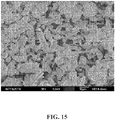
- SEM micrographs will show the change in morphology of the phosphor crystals as the amount of Ca is increased beyond the amount used to charge balance the substitution of Si by Al.
- Sample 1 is a well-known 2-5-8 red-emitting nitride phosphor used herein as a control; it has the composition Sr 1.95 Si 5 N 8 Eu 0.05 .
- Samples 2 through 5 are based on the composition of Sample 1, but with increasing amounts of calcium added as modifier cations; in these samples the modifier cations do not have a charge compensation role to play, for Si substitution at least. These samples have a composition represented by the formula Ca x Sr 1.95 Si 5 N 8 Eu 0.05 .
- Samples 6 through 8 are based on the composition of Sample 1, but with calcium substituting for strontium in increasing amounts; in these samples the modifier cations do not have a charge compensation role to play. These samples have a composition represented by the formula Ca x Sr 1.95-x Si 5 N 8 Eu 0.05 . These Samples are compared with Samples 2 through 4 which have the same amount of calcium added, but in Samples 2 through 4 the calcium does not substitute for strontium -it is in addition to the strontium and is expected to be present in the phosphor crystal in interstitial lattice positions.
- Samples 9 through 12 are based on the composition of Sample 1, but with (1) some aluminum substituted for silicon, and (2) with increasing amounts of calcium added as modifier cations, where the calcium is BOTH playing the role of charge compensation for the substitution of aluminum for silicon, and is present in amounts beyond what is needed for charge compensation and may result in improved phosphor stability under conditions of heat and humidity.
- These samples have a composition represented by the formula Ca x Sr 1.95 Si 4.9 Al 0.1 N 8 Eu 0.05 .
- Samples 13 through 15 are similar to Samples 9 through 12, except for the amount of aluminum being slightly greater in Samples 13 through 15. These samples have a composition represented by the formula Ca x Sr 1.95 Si 4.88 Al 0.12 N 8 Eu 0.05 . Furthermore, Sample 13 has only enough additional calcium to charge compensate the substitution of aluminum for silicon, whereas Samples 14 and 15 have amounts of calcium beyond what is needed for charge compensation.
- the phosphors under blue excitation, may be configured to emit light having a peak emission wavelength greater than about 620 nm, in embodiments greater than 623 nm, and in further embodiments greater than about 626 nm, where blue may be defined as light having a wavelength ranging from about 420 nm to about 470 nm.
- the present phosphors may also be excited by radiation having shorter wavelengths; e.g., from about 200 nm to about 420 nm, but when the excitation radiation is in the x-ray or UV, a separate blue-emitting phosphor is provided to contribute a blue component to the desired white light for a white light source.
- the present phosphors may also be excited by radiation having longer wavelengths, wherein the wavelength ranges from about 200 nm to about 480 nm.
- a common blue excitation source is an InGaN LED, or GaN LED, emitting with a peak at about 460 nm.
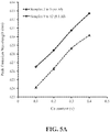
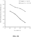
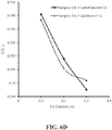
- FIGS. 5A-5D show trends based on the phosphor calcium content of the peak emission wavelength, peak photoluminescence intensity (PL) and CIE x and y chromaticity coordinates, for red-emitting nitride-based calcium-stabilized phosphors Samples 2 through 5 (no aluminum) and 9 through 12 (aluminum containing), according to some embodiments of the present invention. All of these phosphors have excess calcium, beyond what is required for charge balance in the case of the aluminum-containing samples; and all of these phosphors are assumed to have the calcium present in the crystal structure at interstitial sites. The trends for the no aluminum and the aluminum-containing samples are very similar, suggesting that the trends may be dominated by the interstitial calcium content.
- PL peak photoluminescence intensity
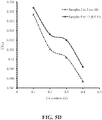
- FIGS. 6A-6D show trends with phosphor calcium content of the peak emission wavelength, peak photoluminescence intensity (PL) and CIE x and y chromaticity coordinates, for red-emitting nitride-based calcium-stabilized phosphors Samples 2 through 4 (additional calcium) and 6 through 8 (substitutional calcium), according to some embodiments of the present invention. There is an appreciable difference in the trends between the additional (assumed interstitial) calcium and the substitutional calcium, suggesting the location of the calcium within the crystal lattice may be significant.
- the ENERGY STAR ® "Program Requirements for Integral LED Lamps" requires that for all LED lamps "the change of chromaticity over the minimum lumen maintenance test period (6000 hours) shall be within 0.007 on the CIE 1976 (u',v') diagram” and depending on lamp type, the lamp must have " ⁇ 70% lumen maintenance (L70) at 15,000 or 25,000 hours of operation”.
- the ENERGY STAR ® requirements are for the lamp performance and include all components of the lamp such as the LEDs, phosphor, electronic driver circuitry, optics and mechanical components. In principal, the degradation in brightness of a white LED with aging can be due not only to the phosphor, but also to the blue LED chip.
- CIE ⁇ x, CIE ⁇ y change in chromaticity
- the accelerated testing is done on phosphor coated 3000K white LEDs prepared as follows: phosphor particles are combined with a binder, such as epoxy or silicone, and then applied to the LED chip. The coated LED is placed in an oven at the specified temperature and humidity and operated continuously for the testing period.
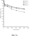
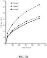
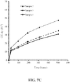
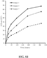
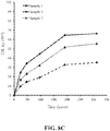
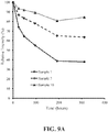
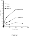
- FIGS. 7A-7C , 8A-8C , 9A-9C and 10A-10C show the results of reliability testing under the conditions of 85°C and 85% relative humidity of phosphor Samples 2 through 4, Samples 1, 3 and 7, Samples 1, 3 and 10 and Samples 13 through 15, respectively.
- the figures show the change in photoluminescent intensity (brightness) with time, the change in CIE x chromaticity coordinate with time, and the change in CIE y chromaticity coordinate with time.
- the Sr 2 Si 5 N 8 :Eu control sample (Sample 1) showed results that would typically be unacceptable to the industry - all other Samples showed different levels of improvement over the control, the best performance being shown by Samples 10 and 15 which will most likely satisfy the typical industry heat and humidity stability requirement.
- FIGS. 7A-7C show an improvement in reliability with increase in additional calcium content of the no aluminum-content phosphors.
- FIGS. 8A-8C compare the control with a substitutional calcium phosphor and an additional calcium phosphor - all phosphors without aluminum and where the two calcium-containing phosphors differ in composition only in that Sample 3 has more strontium than Sample 7, since in Sample 7 the calcium has substituted for strontium; the best reliability is seen for the phosphor with additional calcium.
- FIGS. 9A-9C compare the control with an additional calcium phosphor without aluminum and an additional calcium phosphor with aluminum - the two calcium-containing phosphors differ in composition only in that Sample 10 contains aluminum and Sample 3 does not; the best reliability is seen for the phosphor containing aluminum.
- FIGS. 10A-10C show an improvement in reliability for the additional calcium phosphors with increase in calcium content.
- the most significant improvement in stability over the control (Sample 1), as defined by maintaining intensity and chromaticity, is realized by Ca interstitial charge balancing and Al substituting for Si, plus excess interstitial Ca (beyond what is required for charge balance of the Al); the best stability results are seen for the higher Ca/Al ratio materials, as exemplified by Samples 10 and 15 (see Tables 3B and 4B).
- Samples 10 and 15 are uncoated phosphors, and yet shows excellent stability - stability data is shown for up to 800 hours for Sample 15 and it is expected that after 1000 hours Sample 15 will meet the accelerated testing criteria used to establish ENERGY STAR ® compliance. Even though Samples 10 and 15 show excellent stability without coating, Samples 10 and 15 can be coated to provide expected further stability improvement. Similarly, other Samples can be coated to improve stability.
- the particles of the phosphor with the composition of the Samples of the present invention can be coated with one or more coatings of, for example, SiO 2 , Al 2 O 3 and/or TiO 2 , as taught in U.S. Patent US 9,006,966 for COATINGS FOR PHOTOLUMINESCENT MATERIALS and U.S. Appl. Publication No. 2013092964 for HIGHLY RELIABLE PHOTOLUMINESCENT MATERIALS HAVING A THICK AND UNIFORM TITANIUM DIOXIDE COATING.
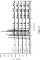
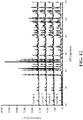
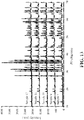
- FIGS. 11-14 show XRD patterns of red-emitting nitride-based phosphors of the present invention; the XRD pattern for Sample 1 is shown for comparison.
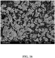
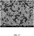
- FIGS. 15-17 show secondary electron micrographs of as prepared red-emitting nitride-based calcium-stabilized phosphors Sample 3 ( FIG. 16 ) (additional calcium) and Sample 7 ( FIG. 17 ) (substitutional calcium), according to some embodiments of the present invention, and prior art red-emitting nitride-based 2-5-8 phosphor Sample 1 ( FIG. 15 ) is shown for comparison. All of FIGS. 15-17 show some particles with a higher aspect ratio (length to width) - in excess of 3. Furthermore, a comparison of FIGS. 15-17 suggests that the percentage of high aspect ratio particles is greater for the control ( FIG. 15 ) than for the samples of the phosphors of the present invention.
- the starting materials included at least one of the compounds Si 3 N 4 , AlN, Ca 3 N 2 , Sr 3 N 2 , BN, GaN, SiO 2 , Al 2 O 3 , and EuCl 3 .
- the furnace was evacuated to 10 -2 Pa, and the sample heated to 150°C under these vacuum conditions.
- a high purity N 2 gas was introduced into the chamber; the temperature of the furnace was then increased to about 1700°C at a substantially constant heating rate of 4°C/min.
- the samples were maintained at 1700°C for about 7 hours.
- a flux such as ammonium chloride, may also be used in the fabrication of the phosphors of the present invention.
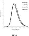
- FIG. 1 is the emission spectra of the phosphors from Samples 1 through 5. Powder x-ray diffraction measurements using the K ⁇ line of a Cu target are shown in FIG. 11 for the phosphors of Samples 1 through 5.
- Table 1A Composition of starting raw materials for Samples 1 through 5 Compound EuCl 3 Sr 3 N 2 Ca 3 N 2 Si 3 N 4 AlN Sample 1 5.166 75.62 0 93.52 0 Sample 2 2.583 37.81 0.988 46.76 0 Sample 3 2.583 37.81 1.976 46.76 0 Sample 4 2.583 37.81 2.964 46.76 0 Sample 5 2.583 37.81 3.952 46.76 0
- Table 1B Emission Peak wavelength, Intensity and CIE of Samples 1 through 5 with Composition Ca x Sr 1.95 Si 5 N 8 Eu 0.05 Test Results Compound Ca Content, x Al Content Emission Peak Wavelength (nm) PL Intensity (a.u.) CIE (x) CIE (y
- the emission spectra of phosphor Samples 6 through 8 are shown in FIG. 2 .
- X-ray diffraction measurements using the K ⁇ line of a Cu target were obtained, and the XRD patterns of Samples 6 through 8 are shown in FIG 12 .
- Table 2A Composition of starting raw materials for Samples 6 through 8 Compound EuCl 3 Sr 3 N 2 Ca 3 N 2 Si 3 N 4 AlN Sample 6 2.583 35.87 0.988 46.76 0 Sample 7 2.583 33.93 1.976 46.76 0 Sample 8 2.583 31.99 2.964 46.76 0
- Table 2B Emission Peak wavelength, Intensity and CIE of Samples 6 through 8 with Composition Ca x Sr 1.95-x Si 5-y Al y N 8 Eu 0.05 Test Results Compound Ca Content, x Al Content Emission Peak Wavelength (nm) PL Intensity (a.u.) CIE (x) CIE (y) Sample 6 0.1 0 624.54 1.66 0.6443 0.355 Sample 7 0.2 0 627.86 1.57 0.6476 0.352 Sample 8 0.3 0 631.08 1.51 0.6500 0.350
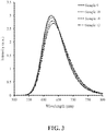
- FIG. 3 is the emission spectra of the phosphors from Samples 9 through 12. x-ray diffraction measurements using the K ⁇ line of a Cu target were obtained, and the XRD patterns of Samples 9 through 12 are shown in FIG. 13 .
- Table 3A Composition of starting raw materials for Samples 9 through 12 Compound EuCl 3 Sr 3 N 2 Ca 3 N 2 Si 3 N 4 AlN Sample 9 2.583 37.81 0.988 45.83 0.82 Sample 10 2.583 37.81 1.976 45.83 0.82 Sample 11 2.583 37.81 2.964 45.83 0.82 Sample 12 2.583 37.81 3.952 45.83 0.82 Table 3B Emission Peak wavelength, Intensity and CIE of Samples 9 through 12 with Composition Ca x Sr 1.95 Si 4.9 Al 0.1 N 8 Eu 0.05 Test Results Compound Ca Content, x Al Content, y Emission Peak Wavelength (nm) PL Intensity (a.u.) CIE (x) CIE (y) Sample 9 0.1 0.1 626.50 1.56 0.6442 0.3554 Sample 10 0.2 0.1 628.42 1.52 0.6470 0.3526 Sample 11 0.3 0.1 630.75 1.46 0.6476 0.3520 Sample 12 0.4 0.1 632.71 1.41 0.6504 0.
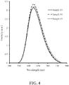
- FIG. 4 is the emission spectra of the phosphors from Samples 13 through 15. X-ray diffraction measurements using the K ⁇ line of a Cu target were obtained, and the XRD patterns of Samples 13 through 15 are shown in FIG. 14 .
- Table 4A Composition of starting raw materials for Samples 13 through 15 Compound EuCl 3 Sr 3 N 2 Ca 3 N 2 Si 3 N 4 AlN Sample 13 5.166 75.622 1.186 91.28 1.968 Sample 14 5.166 75.622 1.976 91.28 1.968 Sample 15 5.166 75.622 3.592 91.28 1.968 Table 4B Emission Peak wavelength, Intensity and CIE of Samples 13 through 15 with Composition Ca x Sr 1.95 Si 4.88 Al 0.12 N 8 Eu 0.05 Test Results Compound Ca Content, x Al Content, y Emission Peak Wavelength (nm) PL Intensity (a.u.) CIE (x) CIE (y) Sample 13 0.06 (charge balanced) 0.12 625 1.66 0.6450 0.3540 Sample 14 0.1 (Ca excess) 0.12 626 1.59 0.6459 0.3538 Sample 15 0.2 (Ca excess) 0.12 629 1.52 0.6478 0.3518
- phosphor compositions may be a red-emitting phosphor comprising a nitride-based composition represented by the chemical formula M a Sr b Si c Al d N e Eu f , wherein: M is Ca, and 0 ⁇ a ⁇ 1.0; 1.5 ⁇ b ⁇ 2.5; 4.0 ⁇ c ⁇ 5.0;0 ⁇ d ⁇ 1.0; 7.5 ⁇ e ⁇ 8.5; and 0 ⁇ f ⁇ 0.1;wherein a+b+f>2+d/v and v is the valence of M.
- M is Ca, and 0 ⁇ a ⁇ 1.0; 1.5 ⁇ b ⁇ 2.5; 4.0 ⁇ c ⁇ 5.0;0 ⁇ d ⁇ 1.0; 7.5 ⁇ e ⁇ 8.5; and 0 ⁇ f ⁇ 0.1;wherein a+b+f>2+d/v and v is the valence of M.
- phosphor compositions that may be made which are represented by the chemical formula M x M' 2 Si 5-y Al y N 8 :A, wherein: M is Mg, Ca, Sr, Ba, Y, Li, Na, K and Zn, and x>0; M' is at least one of Mg, Ca, Sr, Ba, and Zn; 0 ⁇ y ⁇ 0.15; and A is at least one of Eu, Ce, Tb, Pr, and Mn; wherein x>y/v and v is the valence of M, and wherein the phosphors have the general crystalline structure of M' 2 Si 5 N 8 :A.
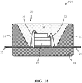
- FIG. 18 illustrates a light emitting device, according to some embodiments.
- the device 10 can comprise a blue light emitting, within the range of 450 nm to 470 nm, GaN (gallium nitride) LED chip 12, for example, housed within a package.
- the package which can for example comprise a low temperature co-fired ceramic (LTCC) or high temperature polymer, comprises upper and lower body parts 16 , 18.
- the upper body part 16 defines a recess 20 , often circular in shape, which is configured to receive the LED chips 12.
- the package further comprises electrical connectors 22 and 24 that also define corresponding electrode contact pads 26 and 28 on the floor of the recess 20.
- LTCC low temperature co-fired ceramic
- the LED chip 12 can be mounted to a thermally conductive pad located on the floor of the recess 20.
- the LED chip's electrode pads are electrically connected to corresponding electrode contact pads 26 and 28 on the floor of the package using bond wires 30 and 32 and the recess 20 is completely filled with a transparent polymer material 34 , typically a silicone, which is loaded with a mixture of a yellow and/or green phosphor and a red phosphor material of the present invention such that the exposed surfaces of the LED chip 12 are covered by the phosphor/polymer material mixture.
- a transparent polymer material 34 typically a silicone
- the walls of the recess are inclined and have a light reflective surface.
- FIGS. 19A and 19B illustrate a solid-state light emitting device, according to some embodiments.
- the device 100 is configured to generate warm white light with a CCT (Correlated Color Temperature) of approximately 3000K and a luminous flux of approximately 1000 lumens and can be used as a part of a downlight or other lighting fixture.
- the device 100 comprises a hollow cylindrical body 102 composed of a circular disc-shaped base 104 , a hollow cylindrical wall portion 106 and a detachable annular top 108.
- the base 104 is preferably fabricated from aluminum, an alloy of aluminum or any material with a high thermal conductivity.
- the base 104 can be attached to the wall portion 106 by screws or bolts or by other fasteners or by means of an adhesive.
- the device 100 further comprises a plurality (four in the example illustrated) of blue light emitting LEDs 112 (blue LEDs) that are mounted in thermal communication with a circular-shaped MCPCB (metal core printed circuit board) 114.
- the blue LEDs 112 can comprise a ceramic packaged array of twelve 0.4W GaN-based (gallium nitride-based) blue LED chips that are configured as a rectangular array 3 rows by 4 columns.
- the device 100 can further comprise light reflective surfaces 116 and 118 that respectively cover the face of the MCPCB 114 and the inner curved surface of the top 108.
- the device 100 further comprises a photoluminescent wavelength conversion component 120 that is operable to absorb a proportion of the blue light generated by the LEDs 112 and convert it to light of a different wavelength by a process of photoluminescence.
- the emission product of the device 100 comprises the combined light generated by the LEDs 112 and the photoluminescent wavelength conversion component 120.
- the wavelength conversion component is positioned remotely to the LEDs 112 and is spatially separated from the LEDs. In this patent specification "remotely" and “remote” means in a spaced or separated relationship.
- the wavelength conversion component 120 is configured to completely cover the housing opening such that all light emitted by the lamp passes through the component 120. As shown the wavelength conversion component 120 can be detachably mounted to the top of the wall portion 106 using the top 108 enabling the component and emission color of the lamp to be readily changed.
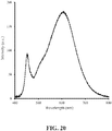
- FIG. 20 shows the emission spectrum from a white light emitting device, such as described above with reference to FIGS. 18 , 19A and 19B , comprising a blue-emitting InGaN LED, a red phosphor having the composition of Sample 14, and one or more yellow/green phosphors with peak emission within the range of 500 nm to 580 nm, such as a phosphor described in U.S. Patent US 8,529,791 and U.S. Patent US 8,475,683 .
- the yellow/green phosphor may be a silicate.
- the white LED may further comprise another phosphor as may be needed to achieve a desired emission spectrum, for example an orange aluminate.
Description
- Embodiments of the present invention are directed to red-emitting nitride-based phosphor compositions.
- Many of the red-emitting phosphors are derived from silicon nitride (Si3N4). The structure of silicon nitride comprises layers of Si and N bonded in a framework of slightly distorted SiN4 tetrahedra. The SiN4 tetrahedra are joined by a sharing of nitrogen corners such that each nitrogen is common to three tetrahedra. See, for example, S. Hampshire in "Silicon nitride ceramics - review of structure, processing, and properties," Journal of Achievements in Materials and Manufacturing Engineering, . Compositions of red-emitting phosphors based on silicon nitride often involve substitution of the Si at the center of the SiN4 tetrahedra by elements such as Al; this is done primarily to modify the optical properties of the phosphors, such as the intensity of the emission, and the peak emission wavelength.
- There is a consequence of the aluminum substitution, however, which is that since Si4+ is being replaced by Al3+, the substituted compound develops a missing positive charge. There are essentially two ways commonly employed to achieve charge balance: in one scheme, an Al3+ for Si4+ substitution is accompanied by a substitution of O2- for N3-, such that the missing positive charge is counter-balanced with a missing negative charge. This leads to a network of tetrahedra that have either Al3+ or Si4+ as the cations at the centers of the tetrahedra, and a structure whereby either an O2- or an N3- anion is at the corners of the tetrahedra. Since it is not known precisely which tetrahedra have which substitutions, the nomenclature used to describe this situation is (Al,Si)3-(N,O)4. Clearly, for charge balance there is one O for N substitution for each Al for Si substitution.
- Furthermore, these substitutional mechanisms for charge balance - O for N - may be employed in conjunction with an interstitial insertion of a cation. In other words, the modifying cation is inserted between atoms preexisting on crystal lattice sites, into "naturally occurring" holes, interstices, or channels. This mechanism does not require an altering of the anionic structure (in other words, a substitution of O for N), but this is not to say that an O for N substitution may not simultaneously occur. Substitutional mechanisms for charge balance may occur in conjunction with an interstitial insertion of a modifier cation.
- The use of modifying cations in nitride phosphors of Sr-containing α-SiAlON has been discussed by K. Shioi et al. in "Synthesis, crystal structure, and photoluminescence of Sr-α-SiAlON:Eu2+," J. Am. Ceram Soc., 93 [2] 465-469 (2010). Shioi et al. give the formula for the overall composition of this class of phosphors: Mm/vSi12-m-nAlm+nOnN16-n:Eu2+, where M is a "modifying cation" such as Li, Mg, Ca, Y, and rare earths (excluding La, Ce, Pr, and Eu), and v is the valence of the M cation. As taught by Shioi et al., the crystal structure of an α-SiAlON is derived from the compound α-Si3N4. To generate an α-SiAlON from α-Si3N4, a partial replacement of Si4+ ions by Al3+ ions takes place, and to compensate for the charge imbalance created by Al3+ substituting for Si4+, some O substitutes N and some positive charges are added by trapping the M cations into the interstices within the network of (Si,Al)-(O,N)4 tetrahedra.
- Europium doped alkaline earth metal silicon nitride phosphor with the general formula M2Si5N8:Eu, where M is Ca, Sr, or Ba, have been widely studied, see for example the PhD thesis by JWH van Krevel at the Technical University Eindhoven, January 2000, and H. A. Hoppe, et al., J. Phys. Chem. Solids. 2000, 61:2001-2006. In this family of phosphors, pure Sr2Si5N8:Eu has high quantum efficiency and emits at a peak wavelength of about 620 nm. However, this red nitride phosphor has poor stability when used as a coating on an LED operated at a temperature in the range from 60°C to 120°C and an ambient relative humidity in the range from 40% to 90%.
- Various research groups have experimented with oxygen-containing M2Si5N8 based phosphor materials, which may also contain other metals. For example, see
U.S. Patents 7,671,529 and6,956247 , andU.S. published applications 2010/0288972 ,2008/0081011 , and2008/0001126 . However, these oxygen containing phosphor materials are known to exhibit poor stability under the combined conditions of high temperature and high relative humidity (RH) - for example 85°C and 85% RH. - The forms of charge compensation reported in the art are not believed to render the phosphor more impervious to thermal/humidity aging, nor do they appear to accomplish the beneficial result of increasing the peak emission wavelength with little or substantially no alteration of photoemission intensity.
-
US2010187974 discloses an oxynitride luminescent material. The oxynitride has a chemical formula of AxByOzN2/3x+4/3y-2/3z:R, wherein A is one or more elements selected from the group consisting of Be, Mg, Ca, Sr, Ba, and Zn; B is one or more elements selected from the group consisting of Si, Ge, Zr, Ti, B, Al, Ga, In, Li, and Na, and at least contains Si. The oxynitride luminescent material can act as cyan to red luminescent material applicable to white light LED that is excited by ultraviolet or blue light LED. Its excitation wavelength is between 300-500 nm, while the emission wavelength at 470-700 nm. With blue or ultraviolet or near-ultraviolet LED, this type of material can be used to produce a white light illumination or display light source. -
WO2006073141 discloses an oxynitride phosphor containing a luminescent center ion in a crystal lattice of an oxynitride. The oxynitride is a compound represented by a chemical formula: M2Si5-pAlpOpN8-p; where M is at least one element selected from the group consisting of Mg, Ca, Sr, Ba, and Zn, and p is a numerical value satisfying an expression: 0 < p < 1. Furthermore, a light-emitting device is formed using a phosphor containing the oxynitride phosphor and a light-emitting element for exciting the phosphor. - There is a need for silicon nitride-based phosphors and M2Si5N8-based phosphors with peak emission wavelengths over a wider range in the red and also other colors, and with enhanced physical properties of the phosphor, such as temperature and humidity stability.
- Embodiments of the present invention provide Ca-stabilized, nitride-based phosphors with chemical composition which may be based on M2Si5N8 with and without column IIIB elements, particularly Al, substituting for Si. The stabilizing cations may be (1) incorporated into the phosphor crystal structure for charge balance for column IIIB element substitution, when used to substitute for Si, and (2) incorporated into the phosphor in excess of any need for charge balancing the substitution of Si by a column IIIB element. These phosphor materials may be configured to extend the peak emission wavelength to longer wavelengths in the red, and to enhance physical properties of the phosphor - notably, significant improvement of the temperature and humidity stability.
- Embodiments of the present invention are directed to a red-emitting phosphor comprising a nitride-based composition represented by the chemical formula MaSrbSicAldNeEuf, wherein: M is Ca, and 0 < a < 1.0; 1.5 < b < 2.5; 4.0 ≤ c ≤ 5.0;0 < d ≤ 1.0; 7.5 < e < 8.5; and 0 < f < 0.1;wherein a+b+f>2+d/v and v is the valence of M. Furthermore, the red-emitting phosphor may have the general crystalline structure of M'2Si5N8:A. Yet furthermore, Al may substitute for Si within the general crystalline structure and M may be located within the general crystalline structure substantially at interstitial sites. Furthermore, the red-emitting phosphor may comprise at least one of F, Cl, Br and O.
- It may be that 0.1≤d≤0.15 and 0.1≤a≤0.4.
- The addition of interstitial Ca to an aluminum substituted M'2Si5N8 red-emitting phosphor, beyond any need for charge balancing for the substitution of Si by Al, has the unexpected benefit that the stability of the phosphor is enhanced under conditions of aging at elevated temperature and humidity. In some embodiments, the phosphor may be compositionally configured such that after 800 hours of aging at 85°C and 85% relative humidity the drop in photoluminescent intensity is no greater than about 15%, in embodiments no greater than about 10%, and the deviation in chromaticity coordinates CIE Δx and CIE Δy is less than or equal to about 0.015 for each coordinate, in embodiments less than or equal to about 0.010 for each coordinate, and in further embodiments less than or equal to about 0.005 for each coordinate.
- Furthermore, the addition of Ca to a M'2Si5N8 red-emitting phosphor has the unexpected benefit that the stability of the phosphor is enhanced under conditions of aging at elevated temperature and humidity. In some embodiments, the phosphor may be compositionally configured such that after 500 hours of aging at 85°C and 85% humidity the drop in photoluminescent intensity is no greater than about 50%, in embodiments no greater than about 35%, and the deviation in chromaticity coordinates CIE Δx and CIE Δy is less than or equal to about 0.065 for each coordinate, and in embodiments less than or equal to about 0.045 for each coordinate.
- According to the present embodiments, the phosphor, under blue excitation, may be configured to emit light having a peak emission wavelength greater than about 620 nm, in embodiments greater than 623 nm, and in further embodiments greater than about 626 nm, where blue may be defined as light having a wavelength ranging from about 420 nm to about 470 nm. The present phosphors may also be excited by radiation having shorter wavelengths; e.g., from about 200 nm to about 420 nm, but when the excitation radiation is in the x-ray or UV, a separate blue-emitting phosphor is provided to contribute a blue component to the desired white light for a white light source. Furthermore, the present phosphors may also be excited by radiation having longer wavelengths, wherein the wavelength ranges from about 200 nm to about 480 nm. A common blue excitation source is an InGaN LED, or GaN LED, emitting with a peak at about 465 nm.
- Embodiments of the present invention also include white light emitting device comprising a solid state excitation source and any of the red-emitting phosphors described herein. It may also include a yellow-emitting phosphor and/or a green-emitting phosphor with a peak emission wavelength in the range from about 500 nm to about 580 nm. An exemplary red-emitting phosphor according to embodiments of the present invention is Eu0.05Ca0.1Sr1.95Si4.88Al0.12N8. The present invention, therefore, encompasses a white light emitting device comprising: a solid state excitation source with emission wavelength within a range from 200 nm to 480 nm; a red-emitting phosphor as described herein, said red-emitting phosphor being configured to absorb excitation radiation from said excitation source and to emit light having a peak emission wavelength in the range from 620 nm to 650 nm; and a yellow/green-emitting phosphor having a peak emission wavelength in the range from 500 nm to 580 nm.
- These and other aspects and features of the present invention will become apparent to those ordinarily skilled in the art upon review of the following description of specific embodiments of the invention in conjunction with the accompanying figures, wherein:
-
FIG. 1 shows emission spectra of the red-emitting nitride-based calcium-stabilizedphosphors Samples 2 through 5, according to some embodiments of the present invention, andSample 1 is a prior art red-emitting nitride-based 2-5-8 phosphor shown for comparison; -
FIG. 2 shows emission spectra of the red-emitting nitride-based calcium-stabilizedphosphors Samples 6 through 8, according to some embodiments of the present invention, andSample 1 is shown for comparison; -
FIG. 3 shows emission spectra of the red-emitting nitride-based calcium-stabilizedphosphors Samples 9 through 12, according to some embodiments of the present invention; -
FIG. 4 shows emission spectra of the red-emitting nitride-based calcium-stabilizedphosphors Samples 13 through 15, according to some embodiments of the present invention; -
FIGS. 5A-5D show trends with phosphor calcium content of the peak emission wavelength, peak photoluminescence intensity (PL) and CIE x and y chromaticity coordinates, for red-emitting nitride-based calcium-stabilizedphosphors Samples 2 through 5 (no aluminum) and 9 through 12 (aluminum containing), according to some embodiments of the present invention; -
FIGS. 6A-6D show trends with phosphor calcium content of the peak emission wavelength, peak photoluminescence intensity (PL) and CIE x and y chromaticity coordinates, for red-emitting nitride-based calcium-stabilizedphosphors Samples 2 through 4 (additional calcium) and 6 through 8 (substitutional calcium), according to some embodiments of the present invention; -
FIGS. 7A-7C show the results of reliability testing under the conditions of 85°C and 85% relative humidity of the red-emitting nitride-based calcium-stabilizedphosphors Samples 2 through 4, whereFIG. 7A is the change in photoluminescent intensity (brightness) with time,FIG. 7B is the change in CIE x chromaticity coordinate with time, andFIG. 7C is the change in CIE y chromaticity coordinate with time, according to some embodiments of the present invention; -
FIGS. 8A-8C show the results of reliability testing under the conditions of 85°C and 85% relative humidity of the red-emitting nitride-based calcium-stabilized phosphors Samples 3 (additional calcium) and 7 (substitutional calcium), whereFIG. 8A is the change in photoluminescent intensity (brightness) with time,FIG. 8B is the change in CIE x chromaticity coordinate with time, andFIG. 8C is the change in CIE y chromaticity coordinate with time, according to some embodiments of the present invention, and reliability data for prior art red-emitting nitride-based 2-5-8phosphor Sample 1 is shown for comparison; -
FIGS. 9A-9C show the results of reliability testing under the conditions of 85°C and 85% relative humidity of the red-emitting nitride-based calcium-stabilized phosphors Samples 3 (no aluminum) and 10 (aluminum containing), whereFIG. 9A is the change in photoluminescent intensity (brightness) with time,FIG. 9B is the change in CIE x chromaticity coordinate with time, andFIG. 9C is the change in CIE y chromaticity coordinate with time, according to some embodiments of the present invention, and reliability data for prior art red-emitting nitride-based 2-5-8phosphor Sample 1 is shown for comparison; -
FIGS. 10A-10C show the results of reliability testing under the conditions of 85°C and 85% relative humidity of the red-emitting nitride-based calcium-stabilizedphosphors Samples 13 through 15, whereFIG. 10A is the change in photoluminescent intensity (brightness) with time,FIG. 10B is the change in CIE x chromaticity coordinate with time, andFIG. 10C is the change in CIE y chromaticity coordinate with time, according to some embodiments of the present invention; -
FIG. 11 shows x-ray diffraction (XRD) patterns of the red-emitting nitride-based calcium-stabilizedphosphor Samples 2 through 5, according to some embodiments of the present invention, the XRD pattern forSample 1 is shown for comparison; -
FIG. 12 shows x-ray diffraction patterns of the red-emitting nitride-based calcium-stabilizedphosphor Samples 6 through 8, according to some embodiments of the present invention, the XRD pattern forSample 1 is shown for comparison; -
FIG. 13 shows x-ray diffraction patterns of the red-emitting nitride-based calcium-stabilizedphosphors Samples 9 through 12, according to some embodiments of the present invention, the XRD pattern forSample 1 is shown for comparison; -
FIG. 14 shows x-ray diffraction patterns of the red-emitting nitride-based calcium-stabilizedphosphors Samples 13 through 15, according to some embodiments of the present invention, the XRD pattern forSample 1 is shown for comparison; -
FIGS. 15-17 show SEM micrographs of red-emitting nitride-based calcium-stabilized phosphors Sample 3 (FIG. 16 ) (additional calcium) and Sample 7 (FIG. 17 ) (substitutional calcium), according to some embodiments of the present invention, and prior art red-emitting nitride-based 2-5-8 phosphor Sample 1 (FIG. 15 ) is shown for comparison; -
FIG. 18 shows a light emitting device, according to some embodiments of the present invention; -
FIGS. 19A and 19B show a solid-state light emitting device, according to some embodiments of the present invention; and -
FIG. 20 shows the emission spectrum from a white LED (3000K) comprising a blue InGaN LED, a red phosphor having the composition ofSample 14, and a yellow/green phosphor, according to some embodiments of the present invention. - Embodiments of the present invention will now be described in detail with reference to the drawings, which are provided as illustrative examples of the invention so as to enable those skilled in the art to practice the invention. Notably, the figures and examples below are not meant to limit the scope of the present invention to a single embodiment, but other embodiments are possible by way of interchange of some or all of the described or illustrated elements. Moreover, where certain elements of the present invention can be partially or fully implemented using known components, only those portions of such known components that are necessary for an understanding of the present invention will be described, and detailed descriptions of other portions of such known components will be omitted so as not to obscure the invention. In the present specification, an embodiment showing a singular component should not be considered limiting; rather, the invention is intended to encompass other embodiments including a plurality of the same component, and vice-versa, unless explicitly stated otherwise herein. Moreover, applicants do not intend for any term in the specification or claims to be ascribed an uncommon or special meaning unless explicitly set forth as such. Further, the present invention encompasses present and future known equivalents to the known components referred to herein by way of illustration.
- Embodiments of the present invention are directed to a red-emitting phosphor comprising a nitride-based composition represented by the chemical formula MaSrbSicAldNeEuf, wherein: M is Ca, and 0 < a < 1.0; 1.5 < b < 2.5; 4.0 ≤ c ≤ 5.0;0 < d ≤ 1.0; 7.5 < e < 8.5; and 0 < f < 0.1;wherein a+b+f>2+d/v and v is the valence of M - the latter reflecting the presence of an excess of M for stabilization of the phosphor and a larger amount of M than needed for charge balance of any Al substituting for Si. Furthermore, the red-emitting phosphor may comprise at least one of F, Cl, Br and O. Yet furthermore, the red-emitting phosphor may have the general crystalline structure of M'2Si5N8:A; although embodiments of the red-emitting phosphor may exist with other crystalline structures. Furthermore, Al may substitute for Si within the general crystalline structure and M may be located within the general crystalline structure substantially at interstitial sites.
- According to some further embodiments of the present invention, nitride-based calcium-stabilized phosphors may have a composition given by the formula CaxSr2Si5-yAlyN8 where x>0 and 0≤y≤1, wherein the Ca is present in an amount greater than is required to charge balance the substitution of Si by Al, in other words where 2x>y, and wherein the phosphors exhibit good stability under heat and humidity, as specified herein.
- In some embodiments, it may be that 0.1≤d≤0.15 and 0.1≤a≤0.4, or 0.1≤d≤0.15 and 0.15≤a≤0.25.
- There is described a nitride-based phosphor composition represented by the general formula MxM'2A5-yDyE8:A, where M is a modifier cation. Advantages of the modification to the 2-5-8 phosphor include an increase in peak emission wavelength towards the deep red end of the spectrum, and an enhanced stability in elevated thermal and humidity conditions.
- M is at least one of a 1+ cation, a 2+ cation, and a 3+ cation, and M' is at least one of Mg, Ca, Sr, Ba, and Zn, used either individually or in combinations. A is at least one of C, Si and Ge, used either individually or in combinations. The element D replaces the A component substitutionally, where D is selected from the group consisting of column IIIB elements of the periodic table of elements. (The labeling of the columns of the periodic table in this disclosure follow the old IUPAC (International Union of Pure and Applied Chemistry) system. See http://en.wikipedia.org/wiki/Group_(periodic_table), last viewed January 15, 2013.). D is at least one of B, Al, and Ga, used either individually or in combinations. E in the general formula is at least one of a 3- anion, a 2- anion, and a 1- anion. Specifically, E may be at least one of O2-, N3-, F1-, Cl1-, Br-, and I-, used either individually or in combinations. The activator, A, is at least one of Eu, Ce, Tb, Pr, Sm and Mn. Herein "A" represents a phosphor activator and the notation ":A" represents doping by a rare earth and/or Mn which is generally substitutional, but may also include doping at grain boundaries, on particle surfaces and in interstitial sites within the crystalline structure of the phosphor material. The parameter y is given by 0≤y≤1.0 and the value of the parameter x may be defined as being greater than the value of y divided by the valence of M, such that M is present in an amount greater than required for charge balance of any substitution of A by D.
- The modifier cation M is added to the phosphor in an amount which is greater than is required to charge compensate for the substitution of D for A. Specifically, M may be at least one of Li1+, Na1+, K1+, Sc3+, Mg2+, Ca2+, Sr2+, Ba2+, Zn2+, B3+ and Y3+, used either individually or in combinations. M is an extra cation, utilized in addition to the stoichiometric amount of the divalent metal M' in the formula M'2Si5N8, and as such, it is expected that this modifier cation might be inserted into the phosphor substantially interstitially, although M may occupy other positions within the host lattice.
- Interstitial sites are cavities, holes, or channels that exist in the crystalline lattice by virtue of the manner in which the host's constituent atoms are arranged (packed, or stacked). Dopant atoms that occupy the interstices of a crystal are to be distinguished from such atoms introduced substitutionally; in this latter mechanism, the dopant atoms replace host atoms residing on crystal lattice sites. Support for the proposed interstitial placement of modifier cations within the structure of the phosphor material is found in the literature for ceramic materials with an α-silicon nitride crystal structure. For example, see Hampshire et al. "α'-Sialon ceramics", Nature 274, 880 (1978) and Huang et al. "Formation of α-Si3N4 Solid Solutions in the System Si3N4-AlN-Y2O3" J. Amer. Ceram. Soc. 66(6), C-96 (1983). These articles state that it is known that the α-silicon nitride unit cell contains two interstitial sites large enough to accommodate other atoms or ions. Furthermore, the α'-sialon structure is derived from the α-silicon nitride structure by partial replacement of Si with Al, and valency compensation is effected by cations - such as Li, Ca, Mg and Y - occupying the interstices of the (Si, Al)-N network, and also by oxygen replacing nitrogen when an oxide is used. (The α'-sialon structure is represented by Mx(Si, Al)12(O, N)16, where x is not greater than 2.) Yet furthermore, it is accepted that the α'-sialon structure requires the equivalent of at least half a cationic valency in each of the two interstices within the unit cell to stabilize the structure.
- Generally, the crystalline structures of the 2-5-8 nitride-based compounds as described herein may have a space group selected from Pmn21 , Cc, derivatives thereof, or mixtures thereof. In some examples, the space group is Pmn21. Furthermore, it should be noted that in materials science theory the vacancy density of a pure crystalline material may be on the order of a hundred parts per million of the existing lattice sites depending on the thermal equilibrium conditions of the crystal. As such, a small percentage of the modifier ions, M, may end up in vacant metal ion sites, rather than the interstitial sites - the modifier ions filling the vacancies before the interstitial sites.
- Furthermore, the modifier ions may also be involved in charge balancing to compensate for the presence of anions of elements such as F, Cl, Br and O within the phosphor, either substituting for N within the M'2Si5N8 crystal lattice, or filling interstitial positions within the crystal lattice. These anions may either be present in the phosphor material intentionally, or as contaminants. Contaminants, such as oxygen, may be from environmental sources. According to some embodiments, the phosphor may have halide and/or oxygen intentionally introduced in a range from 0 to about 6 mole percent. Halide may be added by using one or more starting materials comprising a halide, for example: EuCl3, EuF3, EuBr3, NH4F, etc. Oxygen may be added by using one or more starting materials comprising an oxide, for example: Eu2O3, SiO2, etc. Furthermore, the methods for controllably incorporating oxygen in to the phosphor material that are described in
U.S. patent US 8,663,502 may be used for incorporation of oxygen into the phosphors of the present invention. - Next, the disclosure will present phosphors based on the present modifier cation-stabilized MxM'2A5-yDyE8:A embodiments, giving their advantages and properties, and how these phosphors differ from the prior art. Specific examples will be given, including a phosphor wherein the column IIIB element substituting for Si4+ is Al3+, and wherein the modifying cation is Ca2+, and other examples in which y=0. Accelerated aging results will be discussed which show the superior thermal and chemical stability of the phosphors of the present invention over other prior art 2-5-8 based phosphors. Finally, SEM micrographs will show the change in morphology of the phosphor crystals as the amount of Ca is increased beyond the amount used to charge balance the substitution of Si by Al.
- Fifteen different phosphor samples were prepared as described in more detail below with reference to Tables 1A, 1B, 2A, 2B, 3A, 3B, 4A and 4B. PL spectra, CIE coordinates, XRD and SEM data were collected for samples, as discussed in more detail below.
-
Sample 1 is a well-known 2-5-8 red-emitting nitride phosphor used herein as a control; it has the composition Sr1.95Si5N8Eu0.05.Samples 2 through 5 are based on the composition ofSample 1, but with increasing amounts of calcium added as modifier cations; in these samples the modifier cations do not have a charge compensation role to play, for Si substitution at least. These samples have a composition represented by the formula CaxSr1.95Si5N8Eu0.05. -
Samples 6 through 8 are based on the composition ofSample 1, but with calcium substituting for strontium in increasing amounts; in these samples the modifier cations do not have a charge compensation role to play. These samples have a composition represented by the formula CaxSr1.95-xSi5N8Eu0.05. These Samples are compared withSamples 2 through 4 which have the same amount of calcium added, but inSamples 2 through 4 the calcium does not substitute for strontium -it is in addition to the strontium and is expected to be present in the phosphor crystal in interstitial lattice positions. -
Samples 9 through 12 are based on the composition ofSample 1, but with (1) some aluminum substituted for silicon, and (2) with increasing amounts of calcium added as modifier cations, where the calcium is BOTH playing the role of charge compensation for the substitution of aluminum for silicon, and is present in amounts beyond what is needed for charge compensation and may result in improved phosphor stability under conditions of heat and humidity. These samples have a composition represented by the formula CaxSr1.95Si4.9Al0.1N8Eu0.05. -
Samples 13 through 15 are similar toSamples 9 through 12, except for the amount of aluminum being slightly greater inSamples 13 through 15. These samples have a composition represented by the formula CaxSr1.95Si4.88Al0.12N8Eu0.05. Furthermore,Sample 13 has only enough additional calcium to charge compensate the substitution of aluminum for silicon, whereasSamples - According to some embodiments, the phosphors, under blue excitation, may be configured to emit light having a peak emission wavelength greater than about 620 nm, in embodiments greater than 623 nm, and in further embodiments greater than about 626 nm, where blue may be defined as light having a wavelength ranging from about 420 nm to about 470 nm. The present phosphors may also be excited by radiation having shorter wavelengths; e.g., from about 200 nm to about 420 nm, but when the excitation radiation is in the x-ray or UV, a separate blue-emitting phosphor is provided to contribute a blue component to the desired white light for a white light source. Furthermore, the present phosphors may also be excited by radiation having longer wavelengths, wherein the wavelength ranges from about 200 nm to about 480 nm. A common blue excitation source is an InGaN LED, or GaN LED, emitting with a peak at about 460 nm.
-
FIGS. 5A-5D show trends based on the phosphor calcium content of the peak emission wavelength, peak photoluminescence intensity (PL) and CIE x and y chromaticity coordinates, for red-emitting nitride-based calcium-stabilizedphosphors Samples 2 through 5 (no aluminum) and 9 through 12 (aluminum containing), according to some embodiments of the present invention. All of these phosphors have excess calcium, beyond what is required for charge balance in the case of the aluminum-containing samples; and all of these phosphors are assumed to have the calcium present in the crystal structure at interstitial sites. The trends for the no aluminum and the aluminum-containing samples are very similar, suggesting that the trends may be dominated by the interstitial calcium content. -
FIGS. 6A-6D show trends with phosphor calcium content of the peak emission wavelength, peak photoluminescence intensity (PL) and CIE x and y chromaticity coordinates, for red-emitting nitride-based calcium-stabilizedphosphors Samples 2 through 4 (additional calcium) and 6 through 8 (substitutional calcium), according to some embodiments of the present invention. There is an appreciable difference in the trends between the additional (assumed interstitial) calcium and the substitutional calcium, suggesting the location of the calcium within the crystal lattice may be significant. - Within many territories including the United States, regulatory bodies set performance criteria for replacement LED lamps. For example the US Environmental Protection Agency (EPA) in conjunction with the US Department of Energy (DOE) promulgates performance specifications under which a lamp may be designated as an "ENERGY STAR®" compliant product, e.g. identifying the power usage requirements, minimum light output requirements, luminous intensity distribution requirements, luminous efficacy requirements, life expectancy, etc. The ENERGY STAR® "Program Requirements for Integral LED Lamps" requires that for all LED lamps "the change of chromaticity over the minimum lumen maintenance test period (6000 hours) shall be within 0.007 on the CIE 1976 (u',v') diagram" and depending on lamp type, the lamp must have "≥70% lumen maintenance (L70) at 15,000 or 25,000 hours of operation". The ENERGY STAR® requirements are for the lamp performance and include all components of the lamp such as the LEDs, phosphor, electronic driver circuitry, optics and mechanical components. In principal, the degradation in brightness of a white LED with aging can be due not only to the phosphor, but also to the blue LED chip. Additional sources of degradation can come from the packaging materials (such as the substrate), the bond wires and other components encapsulated with silicone. In contrast, the factors affecting the change in color coordination are dominated primarily by phosphor degradation. In terms of phosphor performance it is believed that in order to comply with ENERGY STAR® requirements would require a change in chromaticity (CIE Δx, CIE Δy) of ≤0.01 for each coordinate over 1000 hours for the phosphor under accelerated testing at 85°C and 85% relative humidity. The accelerated testing is done on phosphor coated 3000K white LEDs prepared as follows: phosphor particles are combined with a binder, such as epoxy or silicone, and then applied to the LED chip. The coated LED is placed in an oven at the specified temperature and humidity and operated continuously for the testing period.
-
FIGS. 7A-7C ,8A-8C ,9A-9C and10A-10C show the results of reliability testing under the conditions of 85°C and 85% relative humidity ofphosphor Samples 2 through 4,Samples Samples Samples 13 through 15, respectively. The figures show the change in photoluminescent intensity (brightness) with time, the change in CIE x chromaticity coordinate with time, and the change in CIE y chromaticity coordinate with time. The Sr2Si5N8:Eu control sample (Sample 1) showed results that would typically be unacceptable to the industry - all other Samples showed different levels of improvement over the control, the best performance being shown bySamples - In more detail,
FIGS. 7A-7C show an improvement in reliability with increase in additional calcium content of the no aluminum-content phosphors.FIGS. 8A-8C compare the control with a substitutional calcium phosphor and an additional calcium phosphor - all phosphors without aluminum and where the two calcium-containing phosphors differ in composition only in thatSample 3 has more strontium thanSample 7, since inSample 7 the calcium has substituted for strontium; the best reliability is seen for the phosphor with additional calcium.FIGS. 9A-9C compare the control with an additional calcium phosphor without aluminum and an additional calcium phosphor with aluminum - the two calcium-containing phosphors differ in composition only in thatSample 10 contains aluminum andSample 3 does not; the best reliability is seen for the phosphor containing aluminum.FIGS. 10A-10C show an improvement in reliability for the additional calcium phosphors with increase in calcium content. In summary, the most significant improvement in stability over the control (Sample 1), as defined by maintaining intensity and chromaticity, is realized by Ca interstitial charge balancing and Al substituting for Si, plus excess interstitial Ca (beyond what is required for charge balance of the Al); the best stability results are seen for the higher Ca/Al ratio materials, as exemplified bySamples 10 and 15 (see Tables 3B and 4B). It should be noted thatSamples Sample 15 and it is expected that after 1000hours Sample 15 will meet the accelerated testing criteria used to establish ENERGY STAR® compliance. Even thoughSamples Samples - To provide a potential further improvement in performance the particles of the phosphor with the composition of the Samples of the present invention can be coated with one or more coatings of, for example, SiO2, Al2O3 and/or TiO2, as taught in U.S. Patent
US 9,006,966 U.S. Appl. Publication No. 2013092964 for HIGHLY RELIABLE PHOTOLUMINESCENT MATERIALS HAVING A THICK AND UNIFORM TITANIUM DIOXIDE COATING. -
FIGS. 11-14 show XRD patterns of red-emitting nitride-based phosphors of the present invention; the XRD pattern forSample 1 is shown for comparison. -
FIGS. 15-17 show secondary electron micrographs of as prepared red-emitting nitride-based calcium-stabilized phosphors Sample 3 (FIG. 16 ) (additional calcium) and Sample 7 (FIG. 17 ) (substitutional calcium), according to some embodiments of the present invention, and prior art red-emitting nitride-based 2-5-8 phosphor Sample 1 (FIG. 15 ) is shown for comparison. All ofFIGS. 15-17 show some particles with a higher aspect ratio (length to width) - in excess of 3. Furthermore, a comparison ofFIGS. 15-17 suggests that the percentage of high aspect ratio particles is greater for the control (FIG. 15 ) than for the samples of the phosphors of the present invention. - For each of the examples and comparative examples described herein, the starting materials included at least one of the compounds Si3N4, AlN, Ca3N2, Sr3N2, BN, GaN, SiO2, Al2O3, and EuCl3.
- To obtain desired compositions of the phosphors exemplified in
Samples 1 through 5, solid powders were weighed according to the compositions listed in Table 1A. This mixture of raw materials were then loaded into a plastic milling bottle together with milling beads, sealed in a glove box, followed by a ball milling process for about 2 hours. The mixed powders were then loaded into a molybdenum crucible having an inner diameter of 30 mm and a height of 30 mm; the loaded crucible was covered with a molybdenum lid and placed into a gas sintering furnace equipped with a graphite heater. - After loading the crucible, the furnace was evacuated to 10-2 Pa, and the sample heated to 150°C under these vacuum conditions. At the 150°C temperature, a high purity N2 gas was introduced into the chamber; the temperature of the furnace was then increased to about 1700°C at a substantially constant heating rate of 4°C/min. The samples were maintained at 1700°C for about 7 hours.
- After firing, the power was shut off and the samples allowed to cool in the furnace. The as-sintered phosphor was ground slightly, ball milled to a certain particle size, followed by a wash, dry and sieve procedure. The final product was tested using an Ocean Optics USB4000 spectrometer for photoluminescence intensity (PL) and chromaticity (CIE coordinates x and y). The x-ray diffraction (XRD) patterns of the phosphors were measured using the Kα line of a Cu target. The test results are listed in Table 1B.
- A flux, such as ammonium chloride, may also be used in the fabrication of the phosphors of the present invention.
-
FIG. 1 is the emission spectra of the phosphors fromSamples 1 through 5. Powder x-ray diffraction measurements using the Kα line of a Cu target are shown inFIG. 11 for the phosphors ofSamples 1 through 5.Table 1A Composition of starting raw materials for Samples 1 through 5Compound EuCl3 Sr3N2 Ca3N2 Si3N4 AlN Sample 1 5.166 75.62 0 93.52 0 Sample 22.583 37.81 0.988 46.76 0 Sample 32.583 37.81 1.976 46.76 0 Sample 42.583 37.81 2.964 46.76 0 Sample 52.583 37.81 3.952 46.76 0 Table 1B Emission Peak wavelength, Intensity and CIE of Samples 1 through 5 with Composition CaxSr1.95Si5N8Eu0.05Test Results Compound Ca Content, x Al Content Emission Peak Wavelength (nm) PL Intensity (a.u.) CIE (x) CIE (y) Sample 10 0 622.77 1.56 0.6423 0.3573 Sample 20.1 0 624.10 1.62 0.6449 0.3547 Sample 30.2 0 626.29 1.61 0.6584 0.3511 Sample 40.3 0 628.64 1.60 0.6493 0.3502 Sample 50.4 0 630.16 1.56 0.6517 0.3477 - To obtain the desired compositions of the phosphors of
Samples 6 through 8, solid powders were weighed according to the compositions listed in Table 2A. The same synthesis procedure as that used forSamples 1 through 5 was used. The test results are listed in Table 2B. - The emission spectra of
phosphor Samples 6 through 8 are shown inFIG. 2 . X-ray diffraction measurements using the Kα line of a Cu target were obtained, and the XRD patterns ofSamples 6 through 8 are shown inFIG 12 .Table 2A Composition of starting raw materials for Samples 6 through 8Compound EuCl3 Sr3N2 Ca3N2 Si3N4 AlN Sample 6 2.583 35.87 0.988 46.76 0 Sample 72.583 33.93 1.976 46.76 0 Sample 82.583 31.99 2.964 46.76 0 Table 2B Emission Peak wavelength, Intensity and CIE of Samples 6 through 8 with Composition CaxSr1.95-xSi5-yAlyN8Eu0.05Test Results Compound Ca Content, x Al Content Emission Peak Wavelength (nm) PL Intensity (a.u.) CIE (x) CIE (y) Sample 60.1 0 624.54 1.66 0.6443 0.355 Sample 70.2 0 627.86 1.57 0.6476 0.352 Sample 80.3 0 631.08 1.51 0.6500 0.350 - To obtain the desired compositions of the phosphors of
Samples 9 through 12, solid powders were weighed according to the compositions listed in Table 3A. The same synthesis procedure as that used forSamples 1 through 5 was used. The test results are listed in Table 3B. -
FIG. 3 is the emission spectra of the phosphors fromSamples 9 through 12. x-ray diffraction measurements using the Kα line of a Cu target were obtained, and the XRD patterns ofSamples 9 through 12 are shown inFIG. 13 .Table 3A Composition of starting raw materials for Samples 9 through 12Compound EuCl3 Sr3N2 Ca3N2 Si3N4 AlN Sample 9 2.583 37.81 0.988 45.83 0.82 Sample 102.583 37.81 1.976 45.83 0.82 Sample 112.583 37.81 2.964 45.83 0.82 Sample 122.583 37.81 3.952 45.83 0.82 Table 3B Emission Peak wavelength, Intensity and CIE of Samples 9 through 12 with Composition CaxSr1.95Si4.9Al0.1N8Eu0.05Test Results Compound Ca Content, x Al Content, y Emission Peak Wavelength (nm) PL Intensity (a.u.) CIE (x) CIE (y) Sample 90.1 0.1 626.50 1.56 0.6442 0.3554 Sample 100.2 0.1 628.42 1.52 0.6470 0.3526 Sample 110.3 0.1 630.75 1.46 0.6476 0.3520 Sample 120.4 0.1 632.71 1.41 0.6504 0.3492 - To obtain the desired compositions of the phosphors of
Samples 13 through 15, solid powders were weighed according to the compositions listed in Table 4A. The same synthesis procedure as that used forSamples 1 through 5 was used. The test results are listed in Table 4B. -
FIG. 4 is the emission spectra of the phosphors fromSamples 13 through 15. X-ray diffraction measurements using the Kα line of a Cu target were obtained, and the XRD patterns ofSamples 13 through 15 are shown inFIG. 14 .Table 4A Composition of starting raw materials for Samples 13 through 15Compound EuCl3 Sr3N2 Ca3N2 Si3N4 AlN Sample 13 5.166 75.622 1.186 91.28 1.968 Sample 145.166 75.622 1.976 91.28 1.968 Sample 155.166 75.622 3.592 91.28 1.968 Table 4B Emission Peak wavelength, Intensity and CIE of Samples 13 through 15 with Composition CaxSr1.95Si4.88Al0.12N8Eu0.05Test Results Compound Ca Content, x Al Content, y Emission Peak Wavelength (nm) PL Intensity (a.u.) CIE (x) CIE (y) Sample 130.06 (charge balanced) 0.12 625 1.66 0.6450 0.3540 Sample 140.1 (Ca excess) 0.12 626 1.59 0.6459 0.3538 Sample 150.2 (Ca excess) 0.12 629 1.52 0.6478 0.3518 - Those of ordinary skill in the art will appreciate that compositions beyond those specifically described above may be made using the methods described above with some different choices of elements. For example, phosphor compositions may be a red-emitting phosphor comprising a nitride-based composition represented by the chemical formula MaSrbSicAldNeEuf, wherein: M is Ca, and 0 < a < 1.0; 1.5 < b < 2.5; 4.0 ≤ c ≤ 5.0;0 < d ≤ 1.0; 7.5 < e < 8.5; and 0 < f < 0.1;wherein a+b+f>2+d/v and v is the valence of M. Furthermore, there is also described phosphor compositions that may be made which are represented by the chemical formula MxM'2Si5-yAlyN8:A, wherein: M is Mg, Ca, Sr, Ba, Y, Li, Na, K and Zn, and x>0; M' is at least one of Mg, Ca, Sr, Ba, and Zn; 0≤y≤0.15; and A is at least one of Eu, Ce, Tb, Pr, and Mn; wherein x>y/v and v is the valence of M, and wherein the phosphors have the general crystalline structure of M'2Si5N8:A.
-
FIG. 18 illustrates a light emitting device, according to some embodiments. Thedevice 10 can comprise a blue light emitting, within the range of 450 nm to 470 nm, GaN (gallium nitride)LED chip 12, for example, housed within a package. The package, which can for example comprise a low temperature co-fired ceramic (LTCC) or high temperature polymer, comprises upper andlower body parts upper body part 16 defines arecess 20, often circular in shape, which is configured to receive the LED chips 12. The package further compriseselectrical connectors recess 20. Using adhesive or solder, theLED chip 12 can be mounted to a thermally conductive pad located on the floor of therecess 20. The LED chip's electrode pads are electrically connected to corresponding electrode contact pads 26 and 28 on the floor of the package usingbond wires recess 20 is completely filled with atransparent polymer material 34, typically a silicone, which is loaded with a mixture of a yellow and/or green phosphor and a red phosphor material of the present invention such that the exposed surfaces of theLED chip 12 are covered by the phosphor/polymer material mixture. To enhance the emission brightness of the device the walls of the recess are inclined and have a light reflective surface. -
FIGS. 19A and 19B illustrate a solid-state light emitting device, according to some embodiments. Thedevice 100 is configured to generate warm white light with a CCT (Correlated Color Temperature) of approximately 3000K and a luminous flux of approximately 1000 lumens and can be used as a part of a downlight or other lighting fixture. Thedevice 100 comprises a hollowcylindrical body 102 composed of a circular disc-shapedbase 104, a hollowcylindrical wall portion 106 and a detachableannular top 108. To aid in the dissipation of heat, thebase 104 is preferably fabricated from aluminum, an alloy of aluminum or any material with a high thermal conductivity. The base 104 can be attached to thewall portion 106 by screws or bolts or by other fasteners or by means of an adhesive. - The
device 100 further comprises a plurality (four in the example illustrated) of blue light emitting LEDs 112 (blue LEDs) that are mounted in thermal communication with a circular-shaped MCPCB (metal core printed circuit board) 114. Theblue LEDs 112 can comprise a ceramic packaged array of twelve 0.4W GaN-based (gallium nitride-based) blue LED chips that are configured as arectangular array 3 rows by 4 columns. - To maximize the emission of light, the
device 100 can further comprise lightreflective surfaces MCPCB 114 and the inner curved surface of the top 108. Thedevice 100 further comprises a photoluminescentwavelength conversion component 120 that is operable to absorb a proportion of the blue light generated by theLEDs 112 and convert it to light of a different wavelength by a process of photoluminescence. The emission product of thedevice 100 comprises the combined light generated by theLEDs 112 and the photoluminescentwavelength conversion component 120. The wavelength conversion component is positioned remotely to theLEDs 112 and is spatially separated from the LEDs. In this patent specification "remotely" and "remote" means in a spaced or separated relationship. Thewavelength conversion component 120 is configured to completely cover the housing opening such that all light emitted by the lamp passes through thecomponent 120. As shown thewavelength conversion component 120 can be detachably mounted to the top of thewall portion 106 using the top 108 enabling the component and emission color of the lamp to be readily changed. -
FIG. 20 shows the emission spectrum from a white light emitting device, such as described above with reference toFIGS. 18 ,19A and 19B , comprising a blue-emitting InGaN LED, a red phosphor having the composition ofSample 14, and one or more yellow/green phosphors with peak emission within the range of 500 nm to 580 nm, such as a phosphor described in U.S. PatentUS 8,529,791 and U.S. PatentUS 8,475,683 . In further embodiments, the yellow/green phosphor may be a silicate. Yet furthermore, the white LED may further comprise another phosphor as may be needed to achieve a desired emission spectrum, for example an orange aluminate.
Claims (12)
- A red-emitting phosphor comprising a nitride-based composition represented by the chemical formula MaSrbSicAldNeEuf, wherein:M is Ca, and 0 < a < 1.0;1.5 < b < 2.5;4.0 ≤ c ≤ 5.0;0 < d ≤ 1.0;7.5 < e < 8.5; and0 < f < 0.1;wherein a+b+f >2+d/v and v is the valence of M.
- A white light emitting device comprising:a solid state excitation source with emission wavelength within a range from 200 nm to 480 nm;a red-emitting phosphor according to Claim 1, said red-emitting phosphor being configured to absorb excitation radiation from said excitation source and to emit light having a peak emission wavelength in the range from 620 nm to 650 nm; anda yellow/green-emitting phosphor having a peak emission wavelength in the range from 500 nm to 580 nm.
- The red-emitting phosphor or white light emitting device of claims 1 or claim 2, further comprising at least one of F, Cl, Br and O.
- The red-emitting phosphor or white light emitting device of any of claims 1 to 3, wherein said red-emitting phosphor is selected from the group consisting of:Eu0.05Ca0.1Sr1.95Si4.9Al0.1N8;Eu0.05Ca0.2Sr1.95Si4.9Al0.1N8;Eu0.05Ca0.3Sr1.95Si4.9Al0.1N8;Eu0.05Ca0.4Sr1.95Si4.9Al0.1N8;Eu0.05Ca0.1Sr1.95Si4.88Al0.12N8;andEu0.05Ca0.2Sr1.95Si4.88Al0.12N8.
- The red-emitting phosphor of claim 4, wherein said red-emitting phosphor is configured such that under excitation by a blue LED the reduction in photoluminescent intensity after 800 hours of aging at 85°C and 85% humidity is no greater than 15%.
- The red-emitting phosphor of claim 4, wherein said red-emitting phosphor is configured such that the deviation in chromaticity coordinates CIE Δx and CIE Δy after 800 hours of aging at 85°C and 85% relative humidity is less than or equal to 0.015 for each coordinate.
- The red-emitting phosphor of claim 4, wherein the deviation in chromaticity coordinates CIE Δx and CIE Δy is less than or equal to 0.005 for each coordinate.
- The red-emitting phosphor of claim 4, wherein said red-emitting phosphor absorbs radiation at a wavelength ranging from 200 nm to 550 nm and emits light with a photoluminescence peak emission wavelength greater than 620.0 nm.
- The red-emitting phosphor or white light emitting device of claim 1 or claim 2, wherein said red-emitting phosphor consists of Ca, Sr, Si, Al, N, Eu and at least one of F, Cl, Br and O.
- The red-emitting phosphor of claim 1, wherein said red-emitting phosphor has the general crystalline structure of Sr2Si5N8: Eu, and wherein Al substitutes for Si within said general crystalline structure and M is located within said general crystalline structure at interstitial sites.
- The white light emitting device of claim 2, wherein said red-emitting phosphor has the formula Eu0.05Ca0.1Sr1.95Si4.88Al0.12N8.
- The white light emitting device of claim 2, wherein said excitation source has an emission wavelength within a range from 450 nm to 470 nm.
Priority Applications (1)
| Application Number | Priority Date | Filing Date | Title |
|---|---|---|---|
| EP16175596.2A EP3153563A1 (en) | 2012-07-18 | 2013-07-17 | Red emitting nitride-based phosphors |
Applications Claiming Priority (4)
| Application Number | Priority Date | Filing Date | Title |
|---|---|---|---|
| US201261673191P | 2012-07-18 | 2012-07-18 | |
| US13/871,961 US8663502B2 (en) | 2011-12-30 | 2013-04-26 | Red-emitting nitride-based phosphors |
| US13/922,231 US8597545B1 (en) | 2012-07-18 | 2013-06-19 | Red-emitting nitride-based calcium-stabilized phosphors |
| PCT/US2013/050789 WO2014014975A1 (en) | 2012-07-18 | 2013-07-17 | Red-emitting nitride-based calcium-stabilized phosphors |
Related Child Applications (2)
| Application Number | Title | Priority Date | Filing Date |
|---|---|---|---|
| EP16175596.2A Division EP3153563A1 (en) | 2012-07-18 | 2013-07-17 | Red emitting nitride-based phosphors |
| EP16175596.2A Division-Into EP3153563A1 (en) | 2012-07-18 | 2013-07-17 | Red emitting nitride-based phosphors |
Publications (3)
| Publication Number | Publication Date |
|---|---|
| EP2732007A1 EP2732007A1 (en) | 2014-05-21 |
| EP2732007A4 EP2732007A4 (en) | 2015-01-21 |
| EP2732007B1 true EP2732007B1 (en) | 2017-05-31 |
Family
ID=49640688
Family Applications (2)
| Application Number | Title | Priority Date | Filing Date |
|---|---|---|---|
| EP13802521.8A Not-in-force EP2732007B1 (en) | 2012-07-18 | 2013-07-17 | Red-emitting nitride-based calcium-stabilized phosphors |
| EP16175596.2A Withdrawn EP3153563A1 (en) | 2012-07-18 | 2013-07-17 | Red emitting nitride-based phosphors |
Family Applications After (1)
| Application Number | Title | Priority Date | Filing Date |
|---|---|---|---|
| EP16175596.2A Withdrawn EP3153563A1 (en) | 2012-07-18 | 2013-07-17 | Red emitting nitride-based phosphors |
Country Status (7)
| Country | Link |
|---|---|
| US (3) | US8597545B1 (en) |
| EP (2) | EP2732007B1 (en) |
| JP (2) | JP5735179B2 (en) |
| KR (1) | KR101424236B1 (en) |
| CN (2) | CN103703101B (en) |
| TW (2) | TWI540199B (en) |
| WO (1) | WO2014014975A1 (en) |
Families Citing this family (37)
| Publication number | Priority date | Publication date | Assignee | Title |
|---|---|---|---|---|
| US8740400B2 (en) | 2008-03-07 | 2014-06-03 | Intematix Corporation | White light illumination system with narrow band green phosphor and multiple-wavelength excitation |
| US20120138874A1 (en) | 2010-12-02 | 2012-06-07 | Intematix Corporation | Solid-state light emitting devices and signage with photoluminescence wavelength conversion and photoluminescent compositions therefor |
| US8663502B2 (en) * | 2011-12-30 | 2014-03-04 | Intematix Corporation | Red-emitting nitride-based phosphors |
| WO2013102222A1 (en) | 2011-12-30 | 2013-07-04 | Intematix Corporation | Nitride phosphors with interstitial cations for charge balance |
| US8597545B1 (en) * | 2012-07-18 | 2013-12-03 | Intematix Corporation | Red-emitting nitride-based calcium-stabilized phosphors |
| US9219202B2 (en) * | 2013-04-19 | 2015-12-22 | Cree, Inc. | Semiconductor light emitting devices including red phosphors that exhibit good color rendering properties and related red phosphors |
| US9753357B2 (en) | 2014-02-27 | 2017-09-05 | Intematix Corporation | Compact solid-state camera flash |
| US9318670B2 (en) * | 2014-05-21 | 2016-04-19 | Intematix Corporation | Materials for photoluminescence wavelength converted solid-state light emitting devices and arrangements |
| CN105985772B (en) * | 2015-02-11 | 2019-08-30 | 大连利德照明研发中心有限公司 | Solid light source fluorescent material, its manufacturing method and the composition comprising the fluorescent material |
| CN107532082A (en) * | 2015-04-27 | 2018-01-02 | 默克专利有限公司 | Phosphor and phosphor conversion LED |
| US10066160B2 (en) | 2015-05-01 | 2018-09-04 | Intematix Corporation | Solid-state white light generating lighting arrangements including photoluminescence wavelength conversion components |
| KR102477353B1 (en) | 2015-08-06 | 2022-12-16 | 삼성전자주식회사 | Red phosphor, light emitting device and lighting apparatus |
| JP6602111B2 (en) * | 2015-08-28 | 2019-11-06 | 三星電子株式会社 | Semiconductor light emitting device |
| KR20180067532A (en) | 2015-09-10 | 2018-06-20 | 인터매틱스 코포레이션 | Phosphor-converted white light emitting devices and photoluminescent compounds for overall illumination and display backlighting |
| JP6611036B2 (en) * | 2015-09-10 | 2019-11-27 | パナソニックIpマネジメント株式会社 | Light emitting device and light source for illumination |
| JP6955501B2 (en) | 2016-02-23 | 2021-10-27 | ルミレッズ ホールディング ベーフェー | Wavelength conversion material for light emitting devices |
| US20190169376A1 (en) | 2016-06-29 | 2019-06-06 | Sabic Global Technologies B.V. | Method to Improve Remote Phosphor Optical Properties in Polycarbonate |
| DE102017122996A1 (en) | 2017-10-04 | 2019-04-04 | Osram Opto Semiconductors Gmbh | Phosphor mixture, conversion element and optoelectronic component |
| US10568172B2 (en) | 2017-12-17 | 2020-02-18 | Intematix Corporation | Dimmable solid-state light emitting devices |
| CN108317768A (en) * | 2017-12-29 | 2018-07-24 | 中国海洋石油集团有限公司 | The active cooling systems of downhole spectrometer |
| DE102018101428A1 (en) * | 2018-01-23 | 2019-07-25 | Osram Opto Semiconductors Gmbh | Optoelectronic component |
| CN108165266B (en) * | 2018-03-23 | 2019-01-08 | 旭宇光电(深圳)股份有限公司 | A kind of fluorine nitride phosphor and the luminescent device comprising the fluorescent powder |
| WO2019213644A1 (en) | 2018-05-04 | 2019-11-07 | Intematix Corporation | High color rendering white light emitting devices and high color rendering photoluminescence compositions |
| US10371325B1 (en) | 2018-06-25 | 2019-08-06 | Intematix Corporation | Full spectrum white light emitting devices |
| US10685941B1 (en) | 2019-07-09 | 2020-06-16 | Intematix Corporation | Full spectrum white light emitting devices |
| KR102158811B1 (en) * | 2018-07-03 | 2020-09-22 | 주식회사 엘엠에스 | Optical disc for fingerprint recognition sensor and optical filter including the same |
| CN109370587B (en) * | 2018-09-06 | 2019-10-29 | 旭宇光电(深圳)股份有限公司 | Nitride near-infrared fluorescent material, the light emitting device containing nitride near-infrared fluorescent material |
| JP7319508B2 (en) * | 2018-11-30 | 2023-08-02 | 日亜化学工業株式会社 | Ceramic sintered body manufacturing method, ceramic sintered body, and light emitting device |
| US11781714B2 (en) | 2019-03-18 | 2023-10-10 | Bridgelux, Inc. | LED-filaments and LED-filament lamps |
| EP3942607A1 (en) | 2019-03-18 | 2022-01-26 | Intematix Corporation | Led-filament |
| US11342311B2 (en) | 2019-03-18 | 2022-05-24 | Intematix Corporation | LED-filaments and LED-filament lamps utilizing manganese-activated fluoride red photoluminescence material |
| JP7242894B2 (en) | 2019-03-18 | 2023-03-20 | インテマティックス・コーポレーション | Packaged white light emitting device with photoluminescent layered structure |
| WO2020190960A1 (en) | 2019-03-18 | 2020-09-24 | Intematix Corporation | Led-filament |
| US10887960B2 (en) * | 2019-03-28 | 2021-01-05 | Lumileds Llc | Color tunable light emitting diode (LED) systems, LED lighting systems, and methods |
| WO2021007123A1 (en) | 2019-07-09 | 2021-01-14 | Intematix Corporation | Full spectrum white light emitting devices |
| CN114341313A (en) | 2019-07-23 | 2022-04-12 | 休斯敦大学体系 | Phosphor emitting narrow green light |
| KR20220088454A (en) | 2019-10-23 | 2022-06-27 | 인터매틱스 코포레이션 | High-color region photoluminescence wavelength-converted white light-emitting device |
Family Cites Families (96)
| Publication number | Priority date | Publication date | Assignee | Title |
|---|---|---|---|---|
| US3207583A (en) | 1963-03-28 | 1965-09-21 | American Agricultural Chem Co | Preparation of technical grade red phosphorus |
| EP1104799A1 (en) | 1999-11-30 | 2001-06-06 | Patent-Treuhand-Gesellschaft für elektrische Glühlampen mbH | Red emitting luminescent material |
| DE10133352A1 (en) | 2001-07-16 | 2003-02-06 | Patent Treuhand Ges Fuer Elektrische Gluehlampen Mbh | Lighting unit with at least one LED as a light source |
| DE10147040A1 (en) | 2001-09-25 | 2003-04-24 | Patent Treuhand Ges Fuer Elektrische Gluehlampen Mbh | Lighting unit with at least one LED as a light source |
| CA2447288C (en) | 2002-03-22 | 2011-10-04 | Nichia Corporation | Nitride phosphor and method for preparation thereof, and light emitting device |
| JP4244653B2 (en) | 2003-02-17 | 2009-03-25 | 日亜化学工業株式会社 | Silicon nitride phosphor and light emitting device using the same |
| US7026755B2 (en) | 2003-08-07 | 2006-04-11 | General Electric Company | Deep red phosphor for general illumination applications |
| US7252787B2 (en) | 2003-10-29 | 2007-08-07 | General Electric Company | Garnet phosphor materials having enhanced spectral characteristics |
| TWI359187B (en) | 2003-11-19 | 2012-03-01 | Panasonic Corp | Method for preparing nitridosilicate-based compoun |
| JP3837588B2 (en) | 2003-11-26 | 2006-10-25 | 独立行政法人物質・材料研究機構 | Phosphors and light emitting devices using phosphors |
| JP4165412B2 (en) | 2004-02-13 | 2008-10-15 | 昭栄化学工業株式会社 | Nitride phosphor, method for producing nitride phosphor, white light emitting device and pigment |
| TWI262609B (en) | 2004-02-27 | 2006-09-21 | Dowa Mining Co | Phosphor and manufacturing method thereof, and light source, LED using said phosphor |
| JP4511849B2 (en) | 2004-02-27 | 2010-07-28 | Dowaエレクトロニクス株式会社 | Phosphor and its manufacturing method, light source, and LED |
| US7229573B2 (en) | 2004-04-20 | 2007-06-12 | Gelcore, Llc | Ce3+ and Eu2+ doped phosphors for light generation |
| KR100865624B1 (en) | 2004-04-27 | 2008-10-27 | 파나소닉 주식회사 | Phosphor composition and method for producing the same, and light-emitting device using the same |
| US6956247B1 (en) | 2004-05-26 | 2005-10-18 | Lumileds Lighting U.S., Llc | Semiconductor light emitting device including photonic band gap material and luminescent material |
| CN101163775B (en) | 2004-05-27 | 2011-12-28 | 皇家飞利浦电子股份有限公司 | Illumination system comprising a radiation source and a fluorescent material |
| JP4414821B2 (en) | 2004-06-25 | 2010-02-10 | Dowaエレクトロニクス株式会社 | Phosphor, light source and LED |
| JP4565141B2 (en) | 2004-06-30 | 2010-10-20 | 独立行政法人物質・材料研究機構 | Phosphors and light emitting devices |
| JP4645089B2 (en) | 2004-07-26 | 2011-03-09 | 日亜化学工業株式会社 | Light emitting device and phosphor |
| JP4422653B2 (en) | 2004-07-28 | 2010-02-24 | Dowaエレクトロニクス株式会社 | Phosphor, production method thereof, and light source |
| US7138756B2 (en) | 2004-08-02 | 2006-11-21 | Dowa Mining Co., Ltd. | Phosphor for electron beam excitation and color display device using the same |
| US7575697B2 (en) | 2004-08-04 | 2009-08-18 | Intematix Corporation | Silicate-based green phosphors |
| US7311858B2 (en) | 2004-08-04 | 2007-12-25 | Intematix Corporation | Silicate-based yellow-green phosphors |
| US8017035B2 (en) | 2004-08-04 | 2011-09-13 | Intematix Corporation | Silicate-based yellow-green phosphors |
| US7390437B2 (en) | 2004-08-04 | 2008-06-24 | Intematix Corporation | Aluminate-based blue phosphors |
| JP4543250B2 (en) | 2004-08-27 | 2010-09-15 | Dowaエレクトロニクス株式会社 | Phosphor mixture and light emitting device |
| US7476338B2 (en) | 2004-08-27 | 2009-01-13 | Dowa Electronics Materials Co., Ltd. | Phosphor and manufacturing method for the same, and light source |
| JP4543251B2 (en) | 2004-08-31 | 2010-09-15 | Dowaエレクトロニクス株式会社 | Phosphor and light source |
| EP2360225B1 (en) | 2004-09-22 | 2013-06-26 | National Institute for Materials Science | Phosphor, production method thereof and light emitting instrument |
| JP4674348B2 (en) * | 2004-09-22 | 2011-04-20 | 独立行政法人物質・材料研究機構 | Phosphor, method for producing the same, and light emitting device |
| EP1808471A4 (en) | 2004-10-15 | 2009-10-21 | Mitsubishi Chem Corp | Fluorescent material, fluorescent device using the same, and image display devide and lighting equipment |
| US7671529B2 (en) | 2004-12-10 | 2010-03-02 | Philips Lumileds Lighting Company, Llc | Phosphor converted light emitting device |
| WO2006077740A1 (en) | 2004-12-28 | 2006-07-27 | Nichia Corporation | Nitride phosphor, method for producing same and light-emitting device using nitride phosphor |
| JP2006213910A (en) | 2005-01-06 | 2006-08-17 | Matsushita Electric Ind Co Ltd | Oxynitride phosphor and light-emitting device |
| CN101103088A (en) * | 2005-01-10 | 2008-01-09 | 皇家飞利浦电子股份有限公司 | Illumination system comprising ceramic luminescence converter |
| JP4756261B2 (en) | 2005-01-27 | 2011-08-24 | 独立行政法人物質・材料研究機構 | Phosphor, method for producing the same, and light emitting device |
| EP1845146B1 (en) | 2005-01-31 | 2015-03-04 | Ube Industries, Ltd. | Red emitting nitride phosphor and process for producing the same |
| US7537698B2 (en) | 2005-02-28 | 2009-05-26 | Hitachi Plant Technologies, Ltd. | Process and equipment for treating ammonium containing liquid |
| WO2006095285A1 (en) | 2005-03-09 | 2006-09-14 | Philips Intellectual Property & Standards Gmbh | Illumination system comprising a radiation source and a fluorescent material |
| JP5013374B2 (en) * | 2005-03-22 | 2012-08-29 | 独立行政法人物質・材料研究機構 | Phosphor, method for producing the same, and light emitting device |
| KR20140063899A (en) | 2005-04-01 | 2014-05-27 | 미쓰비시 가가꾸 가부시키가이샤 | Alloy powder for aw material of inorganic functional material and phosphor |
| US20080191609A1 (en) * | 2005-04-19 | 2008-08-14 | Koninklijke Philips Electronics N.V. | Illumination System Comprising a Red-Emitting Ceramic Luminescence Converter |
| JP4975269B2 (en) * | 2005-04-28 | 2012-07-11 | Dowaホールディングス株式会社 | Phosphor and method for producing the same, and light emitting device using the phosphor |
| EP1884552B1 (en) | 2005-05-12 | 2011-01-05 | National Institute for Materials Science | Beta-type sialon fluorescent substance |
| US8206611B2 (en) | 2005-05-24 | 2012-06-26 | Mitsubishi Chemical Corporation | Phosphor and use thereof |
| KR100927154B1 (en) | 2005-08-03 | 2009-11-18 | 인터매틱스 코포레이션 | Silicate-based orange phosphors |
| KR101264580B1 (en) | 2005-09-27 | 2013-05-14 | 미쓰비시 가가꾸 가부시키가이샤 | Fluorescent substance, process for producing the same, and light emitting device using said fluorescent substance |
| JP4932248B2 (en) | 2005-12-21 | 2012-05-16 | Necライティング株式会社 | Yellow light emitting phosphor, white light emitting element using the same, and illumination device using the same |
| WO2007088966A1 (en) | 2006-02-02 | 2007-08-09 | Mitsubishi Chemical Corporation | Complex oxynitride phosphor, light-emitting device using same, image display, illuminating device, phosphor-containing composition and complex oxynitride |
| TWI317756B (en) | 2006-02-07 | 2009-12-01 | Coretronic Corp | Phosphor, fluorescent gel, and light emitting diode device |
| TW200807104A (en) | 2006-04-19 | 2008-02-01 | Mitsubishi Chem Corp | Color image display device |
| JP5188687B2 (en) | 2006-07-18 | 2013-04-24 | 昭和電工株式会社 | Phosphor, manufacturing method thereof, and light emitting device |
| DE102006036577A1 (en) | 2006-08-04 | 2008-02-07 | Patent-Treuhand-Gesellschaft für elektrische Glühlampen mbH | Red emitting phosphor and light source with such phosphor |
| TWI414583B (en) | 2006-09-15 | 2013-11-11 | Mitsubishi Chem Corp | Phosphor, method for producing the same, phosphor-containing composition, light-emitting device, image display and illuminating devidce |
| US8475683B2 (en) | 2006-10-20 | 2013-07-02 | Intematix Corporation | Yellow-green to yellow-emitting phosphors based on halogenated-aluminates |
| US8529791B2 (en) | 2006-10-20 | 2013-09-10 | Intematix Corporation | Green-emitting, garnet-based phosphors in general and backlighting applications |
| US7648650B2 (en) | 2006-11-10 | 2010-01-19 | Intematix Corporation | Aluminum-silicate based orange-red phosphors with mixed divalent and trivalent cations |
| JP5446066B2 (en) | 2006-12-28 | 2014-03-19 | 日亜化学工業株式会社 | Nitride phosphor and light emitting device using the same |
| US8142685B2 (en) | 2007-01-12 | 2012-03-27 | National Institute For Materials Science | Fluorescent material, process for producing the same, and luminescent device |
| US8153025B2 (en) | 2007-02-06 | 2012-04-10 | Koninklijke Philips Electronics N.V. | Red emitting luminescent materials |
| EP2140502B1 (en) | 2007-04-17 | 2017-04-05 | Philips Lighting Holding B.V. | Illumination system |
| EP2135920B1 (en) | 2007-04-18 | 2016-12-21 | Mitsubishi Chemical Corporation | Process for producing inorganic compound, fluorescent material, fluorescent-material-containing composition, luminescent device, illuminator, and image display |
| CN103254900B (en) | 2007-04-18 | 2014-12-17 | 三菱化学株式会社 | Phosphor and light-emitting device thereof |
| EP2009077A1 (en) | 2007-06-29 | 2008-12-31 | Leuchtstoffwerk Breitungen GmbH | Manganese-doped metal-silicon-nitrides phosphors |
| CN101671562B (en) * | 2007-07-02 | 2013-08-14 | 北京宇极科技发展有限公司 | Nitrogen oxides luminescent material and preparation method and application thereof |
| CN101157854B (en) * | 2007-07-02 | 2010-10-13 | 北京宇极科技发展有限公司 | Oxynitrides luminescent material, preparation method and uses thereof |
| JP2009263610A (en) | 2007-08-01 | 2009-11-12 | Mitsubishi Chemicals Corp | Phosphor and method for producing the same, crystalline silicon nitride and method for producing the same, phosphor-containing composition, light-emitting device using the phosphor, image display device, and illuminating device |
| JP5183128B2 (en) | 2007-08-30 | 2013-04-17 | 凸版印刷株式会社 | Liquid crystal display |
| EP2212400B9 (en) | 2007-10-15 | 2014-04-16 | Leuchtstoffwerk Breitungen GmbH | Rare-earth doped alkaline-earth silicon nitride phosphor, method for producing and radiation converting device comprising such a phosphor |
| EP2058382B1 (en) | 2007-10-15 | 2011-05-11 | Leuchtstoffwerk Breitungen GmbH | Method of manufacturing a rare-earth doped alkaline-earth silicon nitride phosphor, rare-earth doped alkaline-earth silicon nitride phosphor obtainable by such a method and radiation-emitting device comprising such a rare-earth doped alkaline-earth silicon nitride phosphor |
| KR100891810B1 (en) | 2007-11-06 | 2009-04-07 | 삼성전기주식회사 | White light emitting device |
| WO2009093427A1 (en) | 2008-01-21 | 2009-07-30 | Nichia Corporation | Light emitting device |
| US8274215B2 (en) * | 2008-12-15 | 2012-09-25 | Intematix Corporation | Nitride-based, red-emitting phosphors |
| US20090283721A1 (en) * | 2008-05-19 | 2009-11-19 | Intematix Corporation | Nitride-based red phosphors |
| US8691113B2 (en) | 2008-07-02 | 2014-04-08 | Dexerials Corporation | Red phosphor, method for producing red phosphor, white light source, illuminating device, and liquid crystal display device |
| TWI389343B (en) | 2008-08-22 | 2013-03-11 | Warm white light emitting diodes and their halide fluorescent powder | |
| US9428688B2 (en) | 2008-11-17 | 2016-08-30 | Cree, Inc. | Phosphor composition |
| US20100289044A1 (en) | 2009-05-12 | 2010-11-18 | Koninklijke Philips Electronics N.V. | Wavelength conversion for producing white light from high power blue led |
| KR20110000286A (en) * | 2009-06-26 | 2011-01-03 | 삼성전자주식회사 | Process for preparing (oxy) nitride phosphor, (oxy) nitride phosphor obtained from the process, and white light emitting device including the same |
| WO2011014010A2 (en) | 2009-07-28 | 2011-02-03 | 성균관대학교산학협력단 | Oxynitride phosphor powder, nitride phosphor powder and a production method therefor |
| CN101798510A (en) | 2010-03-15 | 2010-08-11 | 彩虹集团公司 | Nitride phosphor material and preparation method thereof |
| KR101093575B1 (en) | 2010-04-07 | 2011-12-13 | 한국에너지기술연구원 | Nitride red phosphors and white light emitting diode using rare-earth-co-doped nitride red phosphors |
| US20120019126A1 (en) * | 2010-07-22 | 2012-01-26 | General Electric Company | Oxynitride phosphors, method of preparation, and light emitting instrument |
| JP2012046625A (en) * | 2010-08-26 | 2012-03-08 | Mitsubishi Chemicals Corp | Method of manufacturing phosphor |
| JP2012046626A (en) * | 2010-08-26 | 2012-03-08 | Mitsubishi Chemicals Corp | Phosphor and light-emitting device using the same |
| JP5799212B2 (en) * | 2010-09-21 | 2015-10-21 | パナソニックIpマネジメント株式会社 | Light emitting module, backlight device and display device |
| US8329484B2 (en) * | 2010-11-02 | 2012-12-11 | Tsmc Solid State Lighting Ltd. | Phosphor with Ce3+/Ce3+, Li+ doped luminescent materials |
| JP2012114333A (en) * | 2010-11-26 | 2012-06-14 | Koito Mfg Co Ltd | Light-emitting module |
| US20130092964A1 (en) | 2011-10-13 | 2013-04-18 | Intematix Corporation | Highly reliable photoluminescent materials having a thick and uniform titanium dioxide coating |
| US9006966B2 (en) | 2011-11-08 | 2015-04-14 | Intematix Corporation | Coatings for photoluminescent materials |
| CN102433114B (en) * | 2011-12-13 | 2015-06-10 | 北京晶创达科技有限公司 | Fluorescent powder, and preparation method and application thereof |
| US8663502B2 (en) * | 2011-12-30 | 2014-03-04 | Intematix Corporation | Red-emitting nitride-based phosphors |
| WO2013102222A1 (en) | 2011-12-30 | 2013-07-04 | Intematix Corporation | Nitride phosphors with interstitial cations for charge balance |
| US8597545B1 (en) * | 2012-07-18 | 2013-12-03 | Intematix Corporation | Red-emitting nitride-based calcium-stabilized phosphors |
| CN104583365B (en) | 2012-07-18 | 2016-05-11 | 英特曼帝克司公司 | Based on the red emitting phosphor of nitride |
-
2013
- 2013-06-19 US US13/922,231 patent/US8597545B1/en active Active
- 2013-07-17 CN CN201380002279.0A patent/CN103703101B/en active Active
- 2013-07-17 CN CN201510510573.3A patent/CN105154079B/en active Active
- 2013-07-17 JP JP2014527372A patent/JP5735179B2/en not_active Expired - Fee Related
- 2013-07-17 WO PCT/US2013/050789 patent/WO2014014975A1/en active Application Filing
- 2013-07-17 KR KR1020137035007A patent/KR101424236B1/en active IP Right Grant
- 2013-07-17 EP EP13802521.8A patent/EP2732007B1/en not_active Not-in-force
- 2013-07-17 EP EP16175596.2A patent/EP3153563A1/en not_active Withdrawn
- 2013-07-18 TW TW103125604A patent/TWI540199B/en not_active IP Right Cessation
- 2013-07-18 TW TW102125825A patent/TWI450945B/en active
- 2013-12-03 US US14/095,766 patent/US9260659B2/en active Active
-
2015
- 2015-04-15 JP JP2015083348A patent/JP6305370B2/en active Active
-
2016
- 2016-02-16 US US15/044,880 patent/US10174246B2/en active Active
Also Published As
| Publication number | Publication date |
|---|---|
| US20160264863A1 (en) | 2016-09-15 |
| EP2732007A1 (en) | 2014-05-21 |
| CN103703101A (en) | 2014-04-02 |
| WO2014014975A1 (en) | 2014-01-23 |
| TW201441342A (en) | 2014-11-01 |
| JP2015157956A (en) | 2015-09-03 |
| EP2732007A4 (en) | 2015-01-21 |
| US8597545B1 (en) | 2013-12-03 |
| TW201406928A (en) | 2014-02-16 |
| WO2014014975A8 (en) | 2014-04-17 |
| CN103703101B (en) | 2015-09-16 |
| KR101424236B1 (en) | 2014-07-28 |
| JP2014524513A (en) | 2014-09-22 |
| US10174246B2 (en) | 2019-01-08 |
| EP3153563A1 (en) | 2017-04-12 |
| TWI540199B (en) | 2016-07-01 |
| US20140084783A1 (en) | 2014-03-27 |
| US9260659B2 (en) | 2016-02-16 |
| TWI450945B (en) | 2014-09-01 |
| CN105154079B (en) | 2017-03-08 |
| JP5735179B2 (en) | 2015-06-17 |
| CN105154079A (en) | 2015-12-16 |
| KR20140028085A (en) | 2014-03-07 |
| JP6305370B2 (en) | 2018-04-04 |
Similar Documents
| Publication | Publication Date | Title |
|---|---|---|
| US10174246B2 (en) | Red-emitting nitride-based calcium-stabilized phosphors | |
| US8663502B2 (en) | Red-emitting nitride-based phosphors | |
| US8419975B2 (en) | Phosphor composition and method for producing the same, and light-emitting device using the same | |
| US20110248303A1 (en) | METHOD FOR PREPARING A B-SiAION PHOSPHOR | |
| TWI530549B (en) | Red-emitting nitride-based phosphors |
Legal Events
| Date | Code | Title | Description |
|---|---|---|---|
| PUAI | Public reference made under article 153(3) epc to a published international application that has entered the european phase |
Free format text: ORIGINAL CODE: 0009012 |
|
| 17P | Request for examination filed |
Effective date: 20131218 |
|
| AK | Designated contracting states |
Kind code of ref document: A1 Designated state(s): AL AT BE BG CH CY CZ DE DK EE ES FI FR GB GR HR HU IE IS IT LI LT LU LV MC MK MT NL NO PL PT RO RS SE SI SK SM TR |
|
| REG | Reference to a national code |
Ref country code: DE Ref legal event code: R079 Ref document number: 602013021795 Country of ref document: DE Free format text: PREVIOUS MAIN CLASS: C09K0011790000 Ipc: C09K0011640000 |
|
| A4 | Supplementary search report drawn up and despatched |
Effective date: 20150105 |
|
| RIC1 | Information provided on ipc code assigned before grant |
Ipc: C09K 11/64 20060101AFI20141218BHEP Ipc: H01L 33/50 20100101ALI20141218BHEP Ipc: H05B 33/14 20060101ALI20141218BHEP |
|
| RIN1 | Information on inventor provided before grant (corrected) |
Inventor name: LI, YI-QUN Inventor name: LIU, SHENGFENG Inventor name: LEUNG, KA, Y. Inventor name: TAO, DEJIE |
|
| RAP1 | Party data changed (applicant data changed or rights of an application transferred) |
Owner name: INTEMATIX CORPORATION |
|
| RAP1 | Party data changed (applicant data changed or rights of an application transferred) |
Owner name: INTEMATIX CORPORATION |
|
| DAX | Request for extension of the european patent (deleted) | ||
| 17Q | First examination report despatched |
Effective date: 20151216 |
|
| GRAP | Despatch of communication of intention to grant a patent |
Free format text: ORIGINAL CODE: EPIDOSNIGR1 |
|
| INTG | Intention to grant announced |
Effective date: 20161222 |
|
| GRAS | Grant fee paid |
Free format text: ORIGINAL CODE: EPIDOSNIGR3 |
|
| GRAA | (expected) grant |
Free format text: ORIGINAL CODE: 0009210 |
|
| AK | Designated contracting states |
Kind code of ref document: B1 Designated state(s): AL AT BE BG CH CY CZ DE DK EE ES FI FR GB GR HR HU IE IS IT LI LT LU LV MC MK MT NL NO PL PT RO RS SE SI SK SM TR |
|
| REG | Reference to a national code |
Ref country code: CH Ref legal event code: EP Ref country code: GB Ref legal event code: FG4D |
|
| REG | Reference to a national code |
Ref country code: AT Ref legal event code: REF Ref document number: 897467 Country of ref document: AT Kind code of ref document: T Effective date: 20170615 |
|
| REG | Reference to a national code |
Ref country code: IE Ref legal event code: FG4D |
|
| REG | Reference to a national code |
Ref country code: DE Ref legal event code: R096 Ref document number: 602013021795 Country of ref document: DE |
|
| REG | Reference to a national code |
Ref country code: NL Ref legal event code: MP Effective date: 20170531 |
|
| REG | Reference to a national code |
Ref country code: LT Ref legal event code: MG4D |
|
| REG | Reference to a national code |
Ref country code: AT Ref legal event code: MK05 Ref document number: 897467 Country of ref document: AT Kind code of ref document: T Effective date: 20170531 |
|
| PG25 | Lapsed in a contracting state [announced via postgrant information from national office to epo] |
Ref country code: FI Free format text: LAPSE BECAUSE OF FAILURE TO SUBMIT A TRANSLATION OF THE DESCRIPTION OR TO PAY THE FEE WITHIN THE PRESCRIBED TIME-LIMIT Effective date: 20170531 Ref country code: ES Free format text: LAPSE BECAUSE OF FAILURE TO SUBMIT A TRANSLATION OF THE DESCRIPTION OR TO PAY THE FEE WITHIN THE PRESCRIBED TIME-LIMIT Effective date: 20170531 Ref country code: GR Free format text: LAPSE BECAUSE OF FAILURE TO SUBMIT A TRANSLATION OF THE DESCRIPTION OR TO PAY THE FEE WITHIN THE PRESCRIBED TIME-LIMIT Effective date: 20170901 Ref country code: AT Free format text: LAPSE BECAUSE OF FAILURE TO SUBMIT A TRANSLATION OF THE DESCRIPTION OR TO PAY THE FEE WITHIN THE PRESCRIBED TIME-LIMIT Effective date: 20170531 Ref country code: NO Free format text: LAPSE BECAUSE OF FAILURE TO SUBMIT A TRANSLATION OF THE DESCRIPTION OR TO PAY THE FEE WITHIN THE PRESCRIBED TIME-LIMIT Effective date: 20170831 Ref country code: HR Free format text: LAPSE BECAUSE OF FAILURE TO SUBMIT A TRANSLATION OF THE DESCRIPTION OR TO PAY THE FEE WITHIN THE PRESCRIBED TIME-LIMIT Effective date: 20170531 Ref country code: LT Free format text: LAPSE BECAUSE OF FAILURE TO SUBMIT A TRANSLATION OF THE DESCRIPTION OR TO PAY THE FEE WITHIN THE PRESCRIBED TIME-LIMIT Effective date: 20170531 |
|
| PG25 | Lapsed in a contracting state [announced via postgrant information from national office to epo] |
Ref country code: LV Free format text: LAPSE BECAUSE OF FAILURE TO SUBMIT A TRANSLATION OF THE DESCRIPTION OR TO PAY THE FEE WITHIN THE PRESCRIBED TIME-LIMIT Effective date: 20170531 Ref country code: BG Free format text: LAPSE BECAUSE OF FAILURE TO SUBMIT A TRANSLATION OF THE DESCRIPTION OR TO PAY THE FEE WITHIN THE PRESCRIBED TIME-LIMIT Effective date: 20170831 Ref country code: RS Free format text: LAPSE BECAUSE OF FAILURE TO SUBMIT A TRANSLATION OF THE DESCRIPTION OR TO PAY THE FEE WITHIN THE PRESCRIBED TIME-LIMIT Effective date: 20170531 Ref country code: NL Free format text: LAPSE BECAUSE OF FAILURE TO SUBMIT A TRANSLATION OF THE DESCRIPTION OR TO PAY THE FEE WITHIN THE PRESCRIBED TIME-LIMIT Effective date: 20170531 Ref country code: SE Free format text: LAPSE BECAUSE OF FAILURE TO SUBMIT A TRANSLATION OF THE DESCRIPTION OR TO PAY THE FEE WITHIN THE PRESCRIBED TIME-LIMIT Effective date: 20170531 Ref country code: IS Free format text: LAPSE BECAUSE OF FAILURE TO SUBMIT A TRANSLATION OF THE DESCRIPTION OR TO PAY THE FEE WITHIN THE PRESCRIBED TIME-LIMIT Effective date: 20170930 |
|
| PG25 | Lapsed in a contracting state [announced via postgrant information from national office to epo] |
Ref country code: RO Free format text: LAPSE BECAUSE OF FAILURE TO SUBMIT A TRANSLATION OF THE DESCRIPTION OR TO PAY THE FEE WITHIN THE PRESCRIBED TIME-LIMIT Effective date: 20170531 Ref country code: CZ Free format text: LAPSE BECAUSE OF FAILURE TO SUBMIT A TRANSLATION OF THE DESCRIPTION OR TO PAY THE FEE WITHIN THE PRESCRIBED TIME-LIMIT Effective date: 20170531 Ref country code: DK Free format text: LAPSE BECAUSE OF FAILURE TO SUBMIT A TRANSLATION OF THE DESCRIPTION OR TO PAY THE FEE WITHIN THE PRESCRIBED TIME-LIMIT Effective date: 20170531 Ref country code: SK Free format text: LAPSE BECAUSE OF FAILURE TO SUBMIT A TRANSLATION OF THE DESCRIPTION OR TO PAY THE FEE WITHIN THE PRESCRIBED TIME-LIMIT Effective date: 20170531 Ref country code: EE Free format text: LAPSE BECAUSE OF FAILURE TO SUBMIT A TRANSLATION OF THE DESCRIPTION OR TO PAY THE FEE WITHIN THE PRESCRIBED TIME-LIMIT Effective date: 20170531 |
|
| PGFP | Annual fee paid to national office [announced via postgrant information from national office to epo] |
Ref country code: DE Payment date: 20171129 Year of fee payment: 5 |
|
| PG25 | Lapsed in a contracting state [announced via postgrant information from national office to epo] |
Ref country code: SM Free format text: LAPSE BECAUSE OF FAILURE TO SUBMIT A TRANSLATION OF THE DESCRIPTION OR TO PAY THE FEE WITHIN THE PRESCRIBED TIME-LIMIT Effective date: 20170531 Ref country code: IT Free format text: LAPSE BECAUSE OF FAILURE TO SUBMIT A TRANSLATION OF THE DESCRIPTION OR TO PAY THE FEE WITHIN THE PRESCRIBED TIME-LIMIT Effective date: 20170531 Ref country code: PL Free format text: LAPSE BECAUSE OF FAILURE TO SUBMIT A TRANSLATION OF THE DESCRIPTION OR TO PAY THE FEE WITHIN THE PRESCRIBED TIME-LIMIT Effective date: 20170531 |
|
| PGFP | Annual fee paid to national office [announced via postgrant information from national office to epo] |
Ref country code: GB Payment date: 20171127 Year of fee payment: 5 |
|
| REG | Reference to a national code |
Ref country code: CH Ref legal event code: PL |
|
| REG | Reference to a national code |
Ref country code: DE Ref legal event code: R097 Ref document number: 602013021795 Country of ref document: DE |
|
| PLBE | No opposition filed within time limit |
Free format text: ORIGINAL CODE: 0009261 |
|
| STAA | Information on the status of an ep patent application or granted ep patent |
Free format text: STATUS: NO OPPOSITION FILED WITHIN TIME LIMIT |
|
| REG | Reference to a national code |
Ref country code: IE Ref legal event code: MM4A |
|
| REG | Reference to a national code |
Ref country code: FR Ref legal event code: ST Effective date: 20180330 |
|
| PG25 | Lapsed in a contracting state [announced via postgrant information from national office to epo] |
Ref country code: LI Free format text: LAPSE BECAUSE OF NON-PAYMENT OF DUE FEES Effective date: 20170731 Ref country code: CH Free format text: LAPSE BECAUSE OF NON-PAYMENT OF DUE FEES Effective date: 20170731 Ref country code: IE Free format text: LAPSE BECAUSE OF NON-PAYMENT OF DUE FEES Effective date: 20170717 |
|
| 26N | No opposition filed |
Effective date: 20180301 |
|
| PG25 | Lapsed in a contracting state [announced via postgrant information from national office to epo] |
Ref country code: SI Free format text: LAPSE BECAUSE OF FAILURE TO SUBMIT A TRANSLATION OF THE DESCRIPTION OR TO PAY THE FEE WITHIN THE PRESCRIBED TIME-LIMIT Effective date: 20170531 Ref country code: FR Free format text: LAPSE BECAUSE OF NON-PAYMENT OF DUE FEES Effective date: 20170731 |
|
| REG | Reference to a national code |
Ref country code: BE Ref legal event code: MM Effective date: 20170731 |
|
| PG25 | Lapsed in a contracting state [announced via postgrant information from national office to epo] |
Ref country code: LU Free format text: LAPSE BECAUSE OF NON-PAYMENT OF DUE FEES Effective date: 20170717 |
|
| PG25 | Lapsed in a contracting state [announced via postgrant information from national office to epo] |
Ref country code: BE Free format text: LAPSE BECAUSE OF NON-PAYMENT OF DUE FEES Effective date: 20170731 |
|
| PG25 | Lapsed in a contracting state [announced via postgrant information from national office to epo] |
Ref country code: MT Free format text: LAPSE BECAUSE OF NON-PAYMENT OF DUE FEES Effective date: 20170717 |
|
| REG | Reference to a national code |
Ref country code: DE Ref legal event code: R119 Ref document number: 602013021795 Country of ref document: DE |
|
| GBPC | Gb: european patent ceased through non-payment of renewal fee |
Effective date: 20180717 |
|
| PG25 | Lapsed in a contracting state [announced via postgrant information from national office to epo] |
Ref country code: DE Free format text: LAPSE BECAUSE OF NON-PAYMENT OF DUE FEES Effective date: 20190201 Ref country code: GB Free format text: LAPSE BECAUSE OF NON-PAYMENT OF DUE FEES Effective date: 20180717 |
|
| PG25 | Lapsed in a contracting state [announced via postgrant information from national office to epo] |
Ref country code: MC Free format text: LAPSE BECAUSE OF FAILURE TO SUBMIT A TRANSLATION OF THE DESCRIPTION OR TO PAY THE FEE WITHIN THE PRESCRIBED TIME-LIMIT Effective date: 20170531 Ref country code: HU Free format text: LAPSE BECAUSE OF FAILURE TO SUBMIT A TRANSLATION OF THE DESCRIPTION OR TO PAY THE FEE WITHIN THE PRESCRIBED TIME-LIMIT; INVALID AB INITIO Effective date: 20130717 |
|
| PG25 | Lapsed in a contracting state [announced via postgrant information from national office to epo] |
Ref country code: CY Free format text: LAPSE BECAUSE OF NON-PAYMENT OF DUE FEES Effective date: 20170531 |
|
| PG25 | Lapsed in a contracting state [announced via postgrant information from national office to epo] |
Ref country code: MK Free format text: LAPSE BECAUSE OF FAILURE TO SUBMIT A TRANSLATION OF THE DESCRIPTION OR TO PAY THE FEE WITHIN THE PRESCRIBED TIME-LIMIT Effective date: 20170531 |
|
| PG25 | Lapsed in a contracting state [announced via postgrant information from national office to epo] |
Ref country code: TR Free format text: LAPSE BECAUSE OF FAILURE TO SUBMIT A TRANSLATION OF THE DESCRIPTION OR TO PAY THE FEE WITHIN THE PRESCRIBED TIME-LIMIT Effective date: 20170531 |
|
| PG25 | Lapsed in a contracting state [announced via postgrant information from national office to epo] |
Ref country code: PT Free format text: LAPSE BECAUSE OF FAILURE TO SUBMIT A TRANSLATION OF THE DESCRIPTION OR TO PAY THE FEE WITHIN THE PRESCRIBED TIME-LIMIT Effective date: 20170531 |
|
| PG25 | Lapsed in a contracting state [announced via postgrant information from national office to epo] |
Ref country code: AL Free format text: LAPSE BECAUSE OF FAILURE TO SUBMIT A TRANSLATION OF THE DESCRIPTION OR TO PAY THE FEE WITHIN THE PRESCRIBED TIME-LIMIT Effective date: 20170531 |