EP2728609A1 - Epitaxial wafer and semiconductor device including the same - Google Patents
Epitaxial wafer and semiconductor device including the same Download PDFInfo
- Publication number
- EP2728609A1 EP2728609A1 EP13191058.0A EP13191058A EP2728609A1 EP 2728609 A1 EP2728609 A1 EP 2728609A1 EP 13191058 A EP13191058 A EP 13191058A EP 2728609 A1 EP2728609 A1 EP 2728609A1
- Authority
- EP
- European Patent Office
- Prior art keywords
- epitaxial
- substrate
- growth
- doping
- gas
- Prior art date
- Legal status (The legal status is an assumption and is not a legal conclusion. Google has not performed a legal analysis and makes no representation as to the accuracy of the status listed.)
- Granted
Links
Images



Classifications
-
- H—ELECTRICITY
- H10—SEMICONDUCTOR DEVICES; ELECTRIC SOLID-STATE DEVICES NOT OTHERWISE PROVIDED FOR
- H10D—INORGANIC ELECTRIC SEMICONDUCTOR DEVICES
- H10D30/00—Field-effect transistors [FET]
- H10D30/60—Insulated-gate field-effect transistors [IGFET]
-
- H—ELECTRICITY
- H10—SEMICONDUCTOR DEVICES; ELECTRIC SOLID-STATE DEVICES NOT OTHERWISE PROVIDED FOR
- H10D—INORGANIC ELECTRIC SEMICONDUCTOR DEVICES
- H10D30/00—Field-effect transistors [FET]
- H10D30/01—Manufacture or treatment
- H10D30/021—Manufacture or treatment of FETs having insulated gates [IGFET]
-
- H—ELECTRICITY
- H10—SEMICONDUCTOR DEVICES; ELECTRIC SOLID-STATE DEVICES NOT OTHERWISE PROVIDED FOR
- H10D—INORGANIC ELECTRIC SEMICONDUCTOR DEVICES
- H10D62/00—Semiconductor bodies, or regions thereof, of devices having potential barriers
- H10D62/80—Semiconductor bodies, or regions thereof, of devices having potential barriers characterised by the materials
- H10D62/83—Semiconductor bodies, or regions thereof, of devices having potential barriers characterised by the materials being Group IV materials, e.g. B-doped Si or undoped Ge
- H10D62/832—Semiconductor bodies, or regions thereof, of devices having potential barriers characterised by the materials being Group IV materials, e.g. B-doped Si or undoped Ge being Group IV materials comprising two or more elements, e.g. SiGe
- H10D62/8325—Silicon carbide
-
- H—ELECTRICITY
- H10—SEMICONDUCTOR DEVICES; ELECTRIC SOLID-STATE DEVICES NOT OTHERWISE PROVIDED FOR
- H10P—GENERIC PROCESSES OR APPARATUS FOR THE MANUFACTURE OR TREATMENT OF DEVICES COVERED BY CLASS H10
- H10P14/00—Formation of materials, e.g. in the shape of layers or pillars
- H10P14/20—Formation of materials, e.g. in the shape of layers or pillars of semiconductor materials
- H10P14/24—Formation of materials, e.g. in the shape of layers or pillars of semiconductor materials using chemical vapour deposition [CVD]
-
- H—ELECTRICITY
- H10—SEMICONDUCTOR DEVICES; ELECTRIC SOLID-STATE DEVICES NOT OTHERWISE PROVIDED FOR
- H10P—GENERIC PROCESSES OR APPARATUS FOR THE MANUFACTURE OR TREATMENT OF DEVICES COVERED BY CLASS H10
- H10P14/00—Formation of materials, e.g. in the shape of layers or pillars
- H10P14/20—Formation of materials, e.g. in the shape of layers or pillars of semiconductor materials
- H10P14/29—Formation of materials, e.g. in the shape of layers or pillars of semiconductor materials characterised by the substrates
- H10P14/2901—Materials
- H10P14/2902—Materials being Group IVA materials
- H10P14/2904—Silicon carbide
-
- H—ELECTRICITY
- H10—SEMICONDUCTOR DEVICES; ELECTRIC SOLID-STATE DEVICES NOT OTHERWISE PROVIDED FOR
- H10P—GENERIC PROCESSES OR APPARATUS FOR THE MANUFACTURE OR TREATMENT OF DEVICES COVERED BY CLASS H10
- H10P14/00—Formation of materials, e.g. in the shape of layers or pillars
- H10P14/20—Formation of materials, e.g. in the shape of layers or pillars of semiconductor materials
- H10P14/32—Formation of materials, e.g. in the shape of layers or pillars of semiconductor materials characterised by intermediate layers between substrates and deposited layers
- H10P14/3202—Materials thereof
- H10P14/3204—Materials thereof being Group IVA semiconducting materials
- H10P14/3208—Silicon carbide
-
- H—ELECTRICITY
- H10—SEMICONDUCTOR DEVICES; ELECTRIC SOLID-STATE DEVICES NOT OTHERWISE PROVIDED FOR
- H10P—GENERIC PROCESSES OR APPARATUS FOR THE MANUFACTURE OR TREATMENT OF DEVICES COVERED BY CLASS H10
- H10P14/00—Formation of materials, e.g. in the shape of layers or pillars
- H10P14/20—Formation of materials, e.g. in the shape of layers or pillars of semiconductor materials
- H10P14/34—Deposited materials, e.g. layers
- H10P14/3402—Deposited materials, e.g. layers characterised by the chemical composition
- H10P14/3404—Deposited materials, e.g. layers characterised by the chemical composition being Group IVA materials
- H10P14/3408—Silicon carbide
-
- H—ELECTRICITY
- H10—SEMICONDUCTOR DEVICES; ELECTRIC SOLID-STATE DEVICES NOT OTHERWISE PROVIDED FOR
- H10P—GENERIC PROCESSES OR APPARATUS FOR THE MANUFACTURE OR TREATMENT OF DEVICES COVERED BY CLASS H10
- H10P14/00—Formation of materials, e.g. in the shape of layers or pillars
- H10P14/20—Formation of materials, e.g. in the shape of layers or pillars of semiconductor materials
- H10P14/34—Deposited materials, e.g. layers
- H10P14/3438—Doping during depositing
- H10P14/3441—Conductivity type
- H10P14/3442—N-type
-
- H—ELECTRICITY
- H10—SEMICONDUCTOR DEVICES; ELECTRIC SOLID-STATE DEVICES NOT OTHERWISE PROVIDED FOR
- H10P—GENERIC PROCESSES OR APPARATUS FOR THE MANUFACTURE OR TREATMENT OF DEVICES COVERED BY CLASS H10
- H10P14/00—Formation of materials, e.g. in the shape of layers or pillars
- H10P14/20—Formation of materials, e.g. in the shape of layers or pillars of semiconductor materials
- H10P14/34—Deposited materials, e.g. layers
- H10P14/3438—Doping during depositing
- H10P14/3441—Conductivity type
- H10P14/3444—P-type
Definitions
- Embodiments relate to an epitaxial wafer and a semiconductor device including the same.
- Epitaxial growth generally includes a chemical vapor deposition process.
- a wafer is heated while a silicon composite of vapor phase/liquid phase/solid phase is transferred to a surface of a single crystal silicon wafer (or substrate) to be thermally decomposed or to have an effect on thermal decomposition.
- an epitaxial wafer is fabricated by laminating silicon onto a single crystal silicon wafer through continuous growth of a single crystal structure.
- a predetermined doping gas is injected into a chamber in the epitaxial growth process.
- doping uniformity of the doped epitaxial wafer it is essential that doping uniformity of the doped epitaxial wafer satisfy a tolerance according to design specification.
- a conventional method wherein doping concentrations of a wafer, a buffer layer and an active layer differ and a doping concentration of the buffer layer is higher than that of the active layer.
- a desired level of doping uniformity cannot be satisfied.
- Embodiments provide a high-quality epitaxial wafer which has improved doping uniformity and thus enhanced properties and yield, and a semiconductor device including the same.
- an epitaxial wafer includes a substrate and an epitaxial structure disposed on the substrate, wherein the epitaxial structure may be doped with an n-type or p-type dopant and have a doping uniformity of 10% or less.
- the doping uniformity may be 9% or less.
- the epitaxial wafer may have the doping uniformity from a center to an edge thereof.
- the epitaxial structure may include a first epitaxial layer and a second epitaxial layer disposed on the first epitaxial layer.
- the first epitaxial layer may be disposed between the substrate and the second epitaxial layer so that leakage current induced when applying voltage to the epitaxial wafer is suppressed.
- the first epitaxial layer may be disposed between the substrate and the second epitaxial layer so that lattice mismatch between the substrate and the second epitaxial layer is reduced, thereby reducing surface defects of the second epitaxial layer.
- the second epitaxial layer may have a surface defect density of 0.5/cm 2 or less.
- a composition of the first epitaxial layer may be the same as that of the second epitaxial layer.
- the first epitaxial layer may be doped at a first doping concentration
- the second epitaxial layer may be doped at a second doping concentration
- the first doping concentration may be greater than the second doping concentration
- the substrate may be a silicon carbide substrate and each of the first and second epitaxial layers may include silicon carbide.
- Each of the first and second epitaxial layers doped with an n-type dopant may include silicon carbon nitride (SiCN) and each of the first and second epitaxial layers doped with a p-type dopant may include aluminum silicon carbide (AlSiC).
- the first epitaxial layer may have a thickness of 1.0 ⁇ m or less.
- the first epitaxial layer may have a thickness of 0.5 ⁇ m to 1.0 ⁇ m.
- a semiconductor device in another embodiment, includes the epitaxial wafer, and a source and a drain disposed on the second epitaxial layer.
- the semiconductor device may be a metal semiconductor field effect transistor (MESFET).
- MESFET metal semiconductor field effect transistor
- a method for fabricating an epitaxial wafer having an epitaxial structure on a substrate in a chamber may include disposing the substrate in the chamber, and doping and growing the epitaxial structure on the substrate by injecting a reactive gas including a growth gas and a doping gas into the chamber with rotating the substrate.
- the growth gas may include silicon and carbon, and a dilution ratio of a source gas in the doping gas, the source gas containing a doping element doped in the epitaxial structure, may be determined according to ratio of carbon to silicon (C/Si) of the epitaxial structure.
- the dilution ratio of the source gas may be determined within 1/100 to 1/10 when the C/Si ratio is 1 or more. In addition, the dilution ratio of the source gas may be determined within 1/70 to 1/30 when the C/Si ratio is lower than 1.
- the rotation speed of the substrate when the reactive gas is injected into the chamber may be determined within 50 rpm to 100 rpm or 50 rpm to 70 rpm.
- the growing of the epitaxial structure may include growing a first epitaxial layer on the substrate and growing a second epitaxial layer on the first epitaxial layer, wherein the growing of the first epitaxial layer and the growing of the second epitaxial layer may be continuously performed without intermission.
- the first epitaxial layer may be grown at a first growth speed
- the second epitaxial layer may be grown at a second growth speed
- the first growth speed may be lower than the second growth speed
- the ratio of carbon to silicon (C/Si) of the epitaxial structure may be controlled to 0.7 to less than 1 during growth of the first epitaxial layer and the ratio of carbon to silicon (C/Si) may be controlled to 1 or more during growth of the second epitaxial layer.
- the doping and growing of the epitaxial structure may further include intermediate growth performed by injecting the reactive gas onto the substrate at a growth speed which increases linearly or stepwise from the first growth speed to the second growth speed, after the growing of the first epitaxial layer and before the growing of the second epitaxial layer.
- the growth gas, the doping gas and diluent gas contained in the reactive gas are injected such that the injection parameter defined by the following equation satisfies 1/45 min/ml to 1/10 min/ml.
- Injection parameter Flux of the reactive gas injected into chamber Flux of the doping gas X Flux of the doping gas + Flux of the diluent gas
- the growth gas and the diluent gas may be injected such that the injection parameter satisfies 1/20 min/ml to 1 min/ml.
- a ratio of flux of the growth gas to flux of the diluent gas contained in the reactive gas is 1/4,000 to 1/3,000 during growth of the first epitaxial layer and a ratio of flux of the growth gas to flux of the diluent gas contained in the reactive gas is 1/1,000 to 1/600 during growth of the second epitaxial layer.
- the ratio of carbon to silicon (C/Si) during growth of the first epitaxial layer may be 0.5 to 0.8
- the ratio (C/Si) during growth of the second epitaxial layer may be 0.8 to 1.2
- a temperature and a pressure at which the epitaxial structure is grown may be 1,600°C to 1,650°C, and 70 mbar to 120mbar, respectively.
- the doping gas may include nitrogen and the diluent gas contained in the reactive gas may include hydrogen.
- the present embodiment provides an epitaxial wafer which has a doping uniformity from a center to an edge of 10% or less, in particular, 9% or less, and a method for fabricating the same.
- mean represents mean of doping concentration
- ⁇ represents a standard deviation of the doping concentration. The more a value of doping uniformity (%) decreases, the more doping is evened.
- the doping uniformity of the epitaxial wafer may be improved by parameters during a doping process such as temperature, pressure, C/Si ratio, Si/H 2 ratio, rotation speed of substrate (or wafer), dilution ratio of doping gas, ratio of diluent gas to source gas and the like.
- the dilution ratio of the source gas corresponding to an actually doped element of the injected doping gas may act as the most essential parameter in order to improve doping uniformity. Accordingly, a method for fabricating an epitaxial wafer according to an embodiment contributes to improvement in doping uniformity through the dilution ratio of the source gas.
- the epitaxial wafer and a method for fabricating the same according to the embodiment will be described with reference to the annexed drawings.
- an epitaxial wafer evenly doped from a center to an edge may be fabricated to have a doping uniformity with an error range of 10% or less.
- the dilution ratio of the source gas in the doping gas injected for this purpose is suitably controlled according to C/Si ratio and a rotation speed of the substrate is also suitably controlled thereby.
- FIGs. 1A to 1C are sectional views illustrating a method 200A for fabricating an epitaxial wafer according to an embodiment.
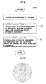
- FIG. 2 is a flowchart illustrating a method 200A for fabricating an epitaxial wafer according to an embodiment.
- FIG. 2 the method 200A for fabricating an epitaxial wafer exemplarily shown in FIG. 2 will be described with reference to FIGs. 1A to 1C , but the embodiment is not limited to the sectional views shown in FIGs. 1A to 1C.
- a substrate 110 is disposed in a reaction chamber (not shown) (step 210).
- the substrate 110 may be a semiconductor substrate and is for example a silicon carbide-based substrate.
- the substrate 110 may be a 4H-SiC substrate as shown in FIGs. 1A to 1C , but the embodiment is not limited thereto. That is, a substrate such as 6H-SiC, 3C-SiC or 15R-SiC other than the 4H-SiC substrate 110 may be used according to type of elements or products finally formed on the epitaxial wafer according to the embodiment.
- a reactive gas (or reactive source) is injected into a chamber and the substrate 110 is rotated, to grow epitaxial layers 115, 117 and 119 on the substrate 110 (Steps 220 to 240).
- an epitaxial structure may include a plurality of epitaxial layers 115, 117 and 119, but the embodiment is not limited thereto.
- a lamination layer (not shown) is formed by laminating or growing a material made of a certain substance on the substrate 110, it may be difficult to secure reliability of the lamination layer due to lattice constant mismatch between the substrate 110 and the lamination layer.
- the epitaxial layer 115 may be laminated as the buffer layer on the substrate 110.
- the first epitaxial layer 117 is grown on the buffer layer 115.
- the second epitaxial layer 119 is grown on the first epitaxial layer 117.
- the growth of the buffer layer 115 may be omitted.
- a reactive gas for epitaxial doping growth on the substrate 110 is injected (Step 220).
- the reactive gas may include a growth gas serving as a source of epitaxial growth and a doping gas used for doping during the growth process, but the embodiment is not limited thereto.
- the afore-mentioned doping gas may include a source gas corresponding to an element which is actually doped on the epitaxial layers 115, 117 and 119 laminated by epitaxial growth and a diluent gas used for diluting the source gas, but the embodiment is not limited thereto.
- a rotation speed of the substrate 110 is controlled (or adjusted) and a dilution ratio of the source gas in the doping gas is controlled (Step 230).
- the step 230 is performed and the step 240 is then performed.
- the steps 220 to 240 may be simultaneously performed.
- the controls of the rotation speed of the substrate 110 and the dilution ratio of the source gas may be performed as follows.
- the substrate 110 on which epitaxial growth is performed is a silicon carbide-based substrate (for example, 4H-SiC substrate), as exemplarily shown in FIGs. 1A to 1C , a liquid, vapor or solid substance (or compound) containing carbon and silicon such as SiH 4 +C 3 H 8 +H 2 , MTS (CH 3 SiCl 3 ), TCS (SiHCl 3 ), Si x C x (1 ⁇ x ⁇ 17), Si x C y (1 ⁇ x ⁇ 17, 1 ⁇ y ⁇ 18) which is a material which matches in lattice constant with the substrate 110 may be used as the growth gas for epitaxial growth.
- a silicon carbide-based substrate for example, 4H-SiC substrate
- a liquid, vapor or solid substance (or compound) containing carbon and silicon such as SiH 4 +C 3 H 8 +H 2 , MTS (CH 3 SiCl 3 ), TCS (SiHCl 3 ), Si x C x (1
- a Group V element such as nitrogen (N 2 ) gas may be used as the source gas, but the embodiment is not limited as to the substance of the source gas.
- the reactive gas may be changed according to material and type of the substrate 110 on which the epitaxial layers 115, 117 and 119 are laminated.
- the source gas actually involved in doping may also be changed according to doping type (n-type or p-type).
- doping type n-type or p-type.
- the description is based on the assumption that a hydrogen (H 2 ) gas is used as the diluent gas for diluting the nitrogen gas used as the source gas, but the embodiment is not limited thereto.
- a hydrogen (H 2 ) gas for example, an inert gas (for example, Ar or He) may be used as the diluent gas.
- the dilution ratio of the source gas may be represented by the following Equation 2.
- Dilution ratio of source gas Flux of doping gas injected into chamber Flux of source gas ? flux of source gas + flux of diluent gas
- the dilution ratio of the source gas corresponding to the doping element actually doped on the epitaxial layers 115, 117 and 119, of the doping gas injected into the chamber may be determined according to ratio of carbon to silicon (C/Si) of the epitaxial structures 115, 117 and 119.
- the ratio (C/Si) of the epitaxial layers 115, 117 and 119 is 1 or more, in the case in which the dilution ratio of the source gas is less than 1 /100 or higher than 1/10, the doping uniformity represented by Equation 1 may be deteriorated.
- the dilution ratio of the source gas may be set within 1/100 to 1/10 when the C/Si ratio of the epitaxial layers 115, 117 and 119 is 1 or more.
- the dilution ratio of the source gas may be controlled to set within 1/70 to 1/30 when the C/Si ratio of the epitaxial layers 115, 117 and 119 is lower than 1.
- the doping gas is supplied through an inlet provided in the chamber and is discharged through an outlet, thereby maintaining a constant concentration of the doping gas in the chamber.
- the doping concentration of an area in which the inlet is disposed may be higher than the doping concentration of an area in which the outlet is disposed, supply of a doping gas at a uniform concentration over the entire surface from a center to an edge of the substrate 110 may be disadvantageously impossible.
- the substrate 110 when the epitaxial layers 115, 117 and 119 are grown, the substrate 110 is rotated.
- the rotation speed of the substrate 110 is less than 50 rpm or is higher than 100 rpm, the doping uniformity of the epitaxial wafer may be deteriorated.
- the rotation speed of the substrate 110 is controlled to set, for example, within 50 rpm to 100 rpm, the constant concentration of the doping gas supplied to the substrate 110 can be maintained.
- FIG. 3 is a graph showing doping uniformity of epitaxial wafers fabricated by the method 200A for fabricating an epitaxial wafer according to the embodiment.
- an x-axis represents the number of tests and a y-axis represents doping uniformity of the epitaxial wafer.
- a test example exemplified shown in FIG. 3 is obtained by performing epitaxial doping and growth at the dilution ratio of the source gas described above, while rotating the substrate 110 at the speed described above. It can be seen from FIG. 3 that doping uniformities of all 10 tests satisfy an error range of 10% or less. As can be seen from the fact that generally-used products have typically doping uniformity with an error range of 15% or less, doping uniformity of epitaxial layers 115, 117 and 119 doped and grown under the conditions according to the embodiment is considerably excellent.
- the epitaxial growth through the condition control as aforementioned is continued until the epitaxial layer is grown to the designed target thickness as shown in the step 240 of FIG. 2 . That is, during the steps 220 and 230, epitaxial layers 115, 117 and 119 are grown on the substrate 110 (Step 240).
- the epitaxial layers 115, 117 and 119 may be formed on the substrate 110 as follows.
- the method 200A for fabricating the epitaxial wafer according to the present embodiment may include a pre-growth step shown in FIGs. 1A and 1B , and a growth step shown in FIG. 1C .
- epitaxial layers 115 and 117 are grown to a predetermined first thickness at a predetermined first growth speed and at a first growth temperature by injecting a reactive gas for epitaxial growth onto the substrate 110 provided in a chamber.
- an epitaxial layer 119 is grown to a target thickness at a predetermined second growth speed and at a second growth temperature by injecting the reactive gas onto the substrate 110.
- the first growth speed is lower than the second growth speed, and the growth step and the pre-growth step are continuously performed without intermission.
- the first growth speed may be for example set to a speed of 3 ⁇ m/h to 5 ⁇ m/h or less (that is, a speed at which the epitaxial layers 115 and 117 are laminated to a thickness of 3 ⁇ m or less or 5 ⁇ m or less per hour).
- Each of the first and second growth speeds may be controlled by controlling flux of the reactive gas injected into the chamber.
- the epitaxial layers 117 and 119 are grown at a high speed, it may be difficult to uniformly laminate or grow the epitaxial layers 117 and 119. Accordingly, in accordance with the pre-growth step, mobility between atoms through the reactive gas is activated by maintaining the predetermined first growth temperature, thereby providing an environment enabling even growth, and time enabling the atoms to be uniformly distributed and grown on the substrate 110 can be secured by reducing the growth speed. Accordingly, because the epitaxial layers 115 and 117 are grown on the substrate 110 by the pre-growth step before the epitaxial layer 119 is grown, lattice mismatch between the substrate 110 and the epitaxial layer 119 is reduced and surface defects of the epitaxial layer 119 is thus considerably reduced.
- the pre-growth step is a preliminary process which reduces surface defects caused by lattice mismatch in an early growth stage and thereby aids to the growth step. Accordingly, the range from about 0.5 ⁇ m to about 1.0 ⁇ m is enough for the thickness of the epitaxial layer (115 or/and 117) grown by the pre-growth step.
- the thicknesses of the epitaxial layer 115 or/and 117 grown through the pre-growth step may be controlled by controlling the first growth temperature, the first growth speed and the growth time.
- the epitaxial layer 119 is properly grown on the epitaxial layers 115 and 117 grown based on the pre-growth step.
- This growth step enables growth of the epitaxial layer 119 at the second growth speed much greater than the first growth speed of the pre-growth step because it is a step after the pre-growth step.
- the second growth speed may be 20 ⁇ m/h or more and the second growth temperature may be set for example to a range from 1,500°C to 1,700°C.
- the growth step may be performed until a total thickness of the epitaxial layers 115, 117 and 119 reaches the desired target thickness. At this time, the target thickness may be changed according to utilization purpose and application of epitaxial wafers, features of final elements and products, design specification and the like.
- the pre-growth step may be controlled so as to set the dilution ratio of the source gas to 1/30 to 1/70 and the growth step may be controlled so as to set the dilution ratio of the source gas to 1 /10 to 1 /100.
- the growth step and the pre-growth step are continuously performed without intermission. That is, the pre-growth step and the growth step may be continuously performed while not stopping injection of the reactive gas (while not stopping the growth step).
- the continuous performance of the growth step may be carried out by the following methods.
- the growth step may be performed immediately after the pre-growth step.
- an intermediate growth step may be interposed between the growth and the pre-growth.
- the intermediate growth step is a process for growing an epitaxial layer by injecting a reactive gas on the substrate 110 at a growth speed which increases linearly or stepwise from the first growth speed which is a growth speed of the pre-growth step to the second growth speed which is a growth speed of the growth step.
- FIG. 4 is a sectional view illustrating an epitaxial wafer 300A according to an embodiment.
- the epitaxial wafer 300A exemplarily shown in FIG. 4 includes a substrate (or wafer) 310 and an epitaxial structure 320 disposed on the substrate 310.
- the substrate 310 may be a semiconductor substrate and may be for example a silicon carbide-based substrate.
- the epitaxial structure 320 may also be a silicon carbide structure.
- the substrate 310 may correspond to the substrate 110 exemplarily shown in FIGs. 1A to 1C .
- the epitaxial structure 320 may include first and second epitaxial layers 322 and 324 and may be doped with an n-type or p-type dopant.
- the first epitaxial layer 322 is disposed on the substrate 310 and the second epitaxial layer 324 is disposed on the first epitaxial layer 322.
- the first epitaxial layer 322 and the second epitaxial layer 324 are epitaxially grown in the growth process by rotating the substrate 310 while controlling the dilution ratio of the source gas, thus maintaining a doping uniformity of 10% or less.
- the first and second epitaxial layers 322 and 324 may correspond to the first and second epitaxial layers 117 and 119, respectively, shown in FIGs. 1B and 1C .
- the first epitaxial layer 322 and the second epitaxial layer 324 may have the same composition because the pre-growth step for forming the first epitaxial layer 322 and the growth step for forming the second epitaxial layer 324 are continuously performed without stopping injection of the reactive gas.
- Leakage current generated upon application of a voltage to the epitaxial wafer 300A can be suppressed by disposing the first epitaxial layer 322 between the substrate 310 and the second epitaxial layer 324.
- the first epitaxial layer 322 may have a thickness of 1 ⁇ m or less, for example, a thickness of 0.5 ⁇ m to 1.0 ⁇ m.
- the second epitaxial layer 324 may be formed to the target thickness through the aforementioned growth step and have a surface defect density of 0.5/cm 2 or less.
- the substrate 310 may be a silicon carbide (SiC) substrate and each of the first epitaxial layer 322 and the second epitaxial layer 324 may include silicon carbide.
- SiC silicon carbide
- each of the first epitaxial layer 322 and the second epitaxial layer 324 may be formed of silicon carbon nitride (SiCN).
- each of the first epitaxial layer 322 and the second epitaxial layer 324 may be formed of aluminum silicon carbide (AlSiC).
- the epitaxial wafer 300A according to the embodiment may have an improved doping uniformity of 10% or less and exhibit high quality such as enhanced properties and yield.
- the doping uniformity of the epitaxial wafer may have an error range of 9% or less.
- the dilution ratio of the source gas in the injected doping gas is suitably controlled according to C/Si ratio and a rotation speed of the substrate is also suitably controlled thereby.
- FIG. 5 is a sectional view of an epitaxial wafer 300B according to another embodiment.
- FIG. 6 is a flowchart illustrating a method 200B for fabricating an epitaxial wafer according to another embodiment.
- the epitaxial wafer 300B includes a substrate (or wafer) 330 and an epitaxial structure 340.
- the substrate 330 may be the same as the substrates 110 and 310 exemplarily shown in FIGs. 1A to 1C or FIG. 4 and may be a semiconductor substrate.
- the substrate 330 is for example a silicon carbide-based substrate.
- the substrate 330 may be various types of substrates such as 4H-SiC, 6H-SiC, 3C-SiC or 15R-SiC according to types of elements or products to be finally fabricated on the epitaxial wafer.
- the epitaxial structure 340 may be disposed on the substrate 330 and may be doped with an n-type or p-type dopant.
- the epitaxial structure 340 may include a buffer layer (or first epitaxial layer) 342 formed by epitaxial growth and an active layer (or second epitaxial layer) 344 formed by epitaxial growth.
- the buffer layer 342 is disposed on the substrate 330 and the active layer 344 is disposed on the buffer layer 342.
- the buffer layer 342 and the active layer 344 may also be formed of a doped silicon carbide-based material.
- the buffer layer 342 may be doped at a first doping concentration and the active layer 344 may be doped at a second doping concentration.
- the buffer layer 342 is provided to reduce crystal defects caused by difference in lattice constant between the substrate 330 and the active layer 344 and the first doping concentration is greater than the second doping concentration.
- the first doping concentration of the buffer layer 342 is 5 ⁇ 10 17 /cm 3 to 7 ⁇ 10 18 /cm 3
- the second doping concentration of the active layer 344 is 1 ⁇ 10 15 /cm 3 to 2 ⁇ 10 16 / cm 3 .
- the buffer layer 342 and the active layer 344 have a doping uniformity of 9% or less.
- each of the buffer layer 342 and the active layer 344 may include silicon carbide.
- each of the buffer layer 342 and the active layer 344 may include n-type conductive silicon carbide, that is, silicon carbon nitride (SiCN), but the embodiment is not limited thereto.
- each of the buffer layer 342 and the active layer 344 may include p-type conductive silicon carbide, that is, aluminum silicon carbide (AlSiC), but the embodiment is not limited thereto.
- the epitaxial wafer 300B exemplarily shown in FIG. 5 may be applied to various semiconductor devices, like the epitaxial wafer 300A exemplarily shown in FIG. 4 .
- the substrate 330 is disposed in the reaction chamber (step 260).
- the step 260 may be the same as the step 210 exemplarily shown in FIG. 2 .
- a reactive gas is injected into the chamber while rotating the substrate 330 at a predetermined rotation speed to dope and grow an epitaxial structure 340 by doping on the substrate 330 (steps 270 and 280).
- the substrate 330 is rotated at a predetermined rotation speed and at the same time, a reactive gas for doping growth of the buffer layer 342 is injected into the chamber to grow the buffer layer 342 on the substrate 330 (step 270).
- the substrate 330 is rotated at a predetermined rotation speed and a reactive gas for doping growth of the active layer 344 is injected into the chamber to grow an active layer 344 on the buffer layer 342 (step 280).
- the reactive gas used for the steps 270 and 280 may include a growth gas (or growth source) serving as a source of epitaxial growth of the buffer layer 342 or the active layer 344, a doping gas (or doping source or source gas) used for doping during the growth step, and a diluent gas used for diluting the doping gas, but the embodiment is not limited thereto.
- the rotation speed of the substrate 330, injection parameters of the reactive gas and the dilution ratio of the growth gas are controlled.
- the controls of the rotation speed of the substrate 330, injection parameters of the reactive gas and the dilution ratio of the growth gas may be carried out using the following method.
- the substrate 330 on which epitaxial structure 340 is grown is a silicon carbide-based substrate (for example, 4H-SiC substrate), a liquid, vapor or solid substance (or compound) containing carbon and silicon such as SiH 4 +C 3 H 8 +H 2 , MTS (CH 3 SiCl 3 ), TCS (SiHCl 3 ), Si x C x (1 ⁇ x ⁇ 17), Si x C y (1 ⁇ x ⁇ 17, 1 ⁇ y ⁇ 18) which is a material which matches in lattice constant with the substrate 330 may be used as the growth gas for epitaxial growth.
- a silicon carbide-based substrate for example, 4H-SiC substrate
- a liquid, vapor or solid substance (or compound) containing carbon and silicon such as SiH 4 +C 3 H 8 +H 2 , MTS (CH 3 SiCl 3 ), TCS (SiHCl 3 ), Si x C x (1 ⁇ x ⁇ 17), Si x C
- a Group V element such as nitrogen (N 2 ) gas may be used as the doping gas, but the embodiment is not limited to the substance of the doping gas.
- the growth gas may be changed according to material and type of the substrate 330 on which the buffer layer 342 and the active layer 344 are laminated.
- the doping gas actually involved in doping may also be changed according to the doping type (n-type or p-type).
- the following description is given based on the assumption that epitaxial doping-growth is performed on the silicon carbide-based substrate 110 using a nitrogen gas as the doping gas.
- the following description is based on the assumption that hydrogen gas (H 2 ) is used as the diluent gas for diluting the nitrogen gas which is the doping gas, but the embodiment is not limited thereto.
- an inert gas for example, Ar or He
- Ar or He an inert gas
- an injection parameter of the reactive gas is controlled to 10 ml/min to 45 ml/min and a ratio of flux of the growth gas to the flux of the diluent gas is controlled to 1/4,000 to 1/3,000 under the conditions that a ratio of carbon to silicon (C/Si) is 0.5 to 0.8, a temperature is 1,600°C to 1,650°C, and a pressure is 70 mbar to 120 mbar.
- an injection parameter of the reactive gas is controlled to 1 ml/min to 20 ml/min and a ratio of flux of the growth gas to flux of the diluent gas is controlled to 1/1,000 to 1/600 under the conditions that the ratio (C/Si) is 0.8 to 1.2, the temperature is 1,600°C to 1,650°C, and the pressure is 70 mbar to 120 mbar.
- Equation 3 a 1 to a 4 represent positive real numbers, and b 1 to b 3 represent real numbers.
- Units of the flux of the reactive gas, the flux of the doping gas and the flux of the diluent gas are ml/min.
- the reactive, doping and diluent gases may be injected such that the injection parameter shown in Equation 3 satisfies 1/45 min/ml to 1/10 min/ml (that is, 10 ml/min to 45 ml/min).
- the reactive, doping and diluent gases may be injected such that the injection parameter described in Equation 3 above satisfies 1/20 min/ml to 1 min/ml (that is, 1 ml/min to 20 ml/min).
- the doping gas is supplied through an inlet provided in the chamber and is discharged through an outlet, thereby maintaining a concentration of the doping gas in the chamber.
- the concentration of doping gas in the vicinity of an area in which the inlet is disposed may be higher than the concentration of doping gas in the vicinity of an area in which the outlet is disposed, it is disadvantageously impossible to supply a doping gas at a uniform concentration over the entire surface from a center to an edge of the substrate 330. Accordingly, during the steps 270 and 280, a concentration of doping gas supplied to the substrate 330 may be uniformly maintained by suitably controlling the rotation speed of the substrate 330.
- the rotation speed of the substrate 330 may be controlled to 50 rpm to 70 rpm (that is, 50 to 70 revolutions per minute).
- Example and Comparative Example wherein epitaxial doping growth is performed on the substrate 330 are exemplarily shown in FIGs. 7 to 10 .
- FIGs. 7 and 8 show the buffer layer 342 and the active layer 344 epitaxially doped and grown on the 4-inch substrate 330 according to the example
- FIGs. 9 and 10 show the buffer layer 342 and the active layer 344 epitaxially doped and grown thereon according to comparative example.
- the buffer layer 342 and the active layer 344 exemplarily shown in FIGs. 7 and 8 are measured using a C-V (capacitance versus voltage) meter.
- the buffer layer 342 of FIG. 7 has a doping uniformity represented by Equation 1 described above, of 8.65% and the active layer 344 of FIG. 8 has a doping uniformity of 8.62%.
- doping uniformities of the buffer layer 342 and the active layer 344 are 9% or less under the conditions of satisfying the rotation speed of the substrate 330, the injection parameter of the reactive gas and the dilution ratio of the growth gas according to the present embodiment.
- the buffer layer 342 and the active layer 344 exemplarily shown in FIGs. 9 and 10 are measured using a C-V (capacitance versus voltage) meter. As a result, the buffer layer 342 exemplarily shown in FIG.
- the active layer 344 exemplarily shown in FIG. 10 has a mean doping concentration of 2.08 ⁇ 10 15 /cm 3 , a standard deviation of 3.12 ⁇ 10 14 /cm 3 and a doping uniformity of 14.98%.
- doping uniformity of the epitaxial structure 300B doped and grown under the conditions according to the present embodiment is considerably excellent.
- the epitaxial doping growth through control of the above conditions may be continued until the active layer 344 is grown to the designed target thickness.
- the growth speed at which the buffer layer 342 is grown may be lower than the growth speed at which the active layer 344 is grown.
- the growth speed at which the buffer layer 342 is set to, for example, 1 ⁇ m/h to 3 ⁇ m/h (that is, a speed at which the epitaxial layer is laminated to a thickness of 1 ⁇ m to 3 ⁇ m per hour).
- the process of growing the buffer layer 342 is effective in reducing lattice mismatch and considerably decreasing surface defects.
- the process of growing the buffer layer 342 is a preliminary process for reducing basal plane dislocation (BPD) caused by lattice mismatch and difference in thermal expansion coefficient between the substrate 330 and the active layer 344. Accordingly, it is enough that the thickness of the buffer layer 342 is about 0.5 ⁇ m to 1.0 ⁇ m.
- the process of growing the active layer 344 enables epitaxial growth at a speed higher than a speed at which the buffer layer 342 is grown.
- the process of growing the active layer 344 may be performed at a speed of 20 ⁇ m/h or more.
- the process of growing the active layer 344 may be performed until a total thickness of the epitaxial structure 340 reaches a desired target growth thickness.
- the target thickness may be changed according to utilization purpose and application of epitaxial wafers, features of final elements and products, design specification and the like.
- the growth of the buffer layer 342 and the growth of the active layer 344 are continuously performed without intermission. That is, the buffer layer growth and the active layer growth may be continuously performed while not stopping injection of the reactive gas (while not stopping the growth step).
- the continuous performance of the growth step may be carried out by the following methods.
- growth of the active layer 344 may be performed immediately after growth of the buffer layer 342.
- an intermediate growth step may be interposed between the growth of the active layer 344 and the growth of the buffer layer 342.
- the intermediate growth step is a process which grows an epitaxial layer by injecting the reactive gas at a growth speed which increases linearly or stepwise from the growth speed in the process of growing the buffer layer 342 after injecting a reactive gas into the chamber to the growth speed in the process of growing the active layer 344.
- the epitaxial wafer 300B according to the another embodiment may have an improved doping uniformity of 9% or less and exhibit high qualities such as enhanced properties and yield.
- the epitaxial wafers 300A and 300B described above may be applied to metal semiconductor field effect transistors (MESFETs).
- the metal semiconductor field effect transistor (MESFET) is fabricated by forming an ohmic contact layer including a source and drain on the second epitaxial layers 324 and 344 according to the present embodiment.
- epitaxial wafers 300A and 300B according to the embodiments may be applied to various semiconductor devices.
Landscapes
- Chemical Vapour Deposition (AREA)
- Recrystallisation Techniques (AREA)
- Crystals, And After-Treatments Of Crystals (AREA)
Abstract
Description
- Embodiments relate to an epitaxial wafer and a semiconductor device including the same.
- Epitaxial growth generally includes a chemical vapor deposition process. In accordance with the epitaxial growth, a wafer is heated while a silicon composite of vapor phase/liquid phase/solid phase is transferred to a surface of a single crystal silicon wafer (or substrate) to be thermally decomposed or to have an effect on thermal decomposition. At this time, an epitaxial wafer is fabricated by laminating silicon onto a single crystal silicon wafer through continuous growth of a single crystal structure. In the case in which an epitaxial wafer having a certain polarity such as n-type or p-type is fabricated, a predetermined doping gas is injected into a chamber in the epitaxial growth process.
- It is essential that doping uniformity of the doped epitaxial wafer satisfy a tolerance according to design specification. For this purpose, there is a conventional method wherein doping concentrations of a wafer, a buffer layer and an active layer differ and a doping concentration of the buffer layer is higher than that of the active layer. However, in spite of using this method, a desired level of doping uniformity cannot be satisfied.
- Embodiments provide a high-quality epitaxial wafer which has improved doping uniformity and thus enhanced properties and yield, and a semiconductor device including the same.
- In one embodiment, an epitaxial wafer includes a substrate and an epitaxial structure disposed on the substrate, wherein the epitaxial structure may be doped with an n-type or p-type dopant and have a doping uniformity of 10% or less. The doping uniformity may be 9% or less.
- The epitaxial wafer may have the doping uniformity from a center to an edge thereof.
- The epitaxial structure may include a first epitaxial layer and a second epitaxial layer disposed on the first epitaxial layer.
- The first epitaxial layer may be disposed between the substrate and the second epitaxial layer so that leakage current induced when applying voltage to the epitaxial wafer is suppressed.
- The first epitaxial layer may be disposed between the substrate and the second epitaxial layer so that lattice mismatch between the substrate and the second epitaxial layer is reduced, thereby reducing surface defects of the second epitaxial layer.
- The second epitaxial layer may have a surface defect density of 0.5/cm2 or less.
- A composition of the first epitaxial layer may be the same as that of the second epitaxial layer.
- The first epitaxial layer may be doped at a first doping concentration, the second epitaxial layer may be doped at a second doping concentration, and the first doping concentration may be greater than the second doping concentration.
- The substrate may be a silicon carbide substrate and each of the first and second epitaxial layers may include silicon carbide.
- Each of the first and second epitaxial layers doped with an n-type dopant may include silicon carbon nitride (SiCN) and each of the first and second epitaxial layers doped with a p-type dopant may include aluminum silicon carbide (AlSiC).
- The first epitaxial layer may have a thickness of 1.0 µm or less.
- The first epitaxial layer may have a thickness of 0.5 µm to 1.0 µm.
- In another embodiment, a semiconductor device includes the epitaxial wafer, and a source and a drain disposed on the second epitaxial layer.
- The semiconductor device may be a metal semiconductor field effect transistor (MESFET).
- In another embodiment, a method for fabricating an epitaxial wafer having an epitaxial structure on a substrate in a chamber may include disposing the substrate in the chamber, and doping and growing the epitaxial structure on the substrate by injecting a reactive gas including a growth gas and a doping gas into the chamber with rotating the substrate.
- The growth gas may include silicon and carbon, and a dilution ratio of a source gas in the doping gas, the source gas containing a doping element doped in the epitaxial structure, may be determined according to ratio of carbon to silicon (C/Si) of the epitaxial structure.
- The dilution ratio of the source gas may be determined within 1/100 to 1/10 when the C/Si ratio is 1 or more. In addition, the dilution ratio of the source gas may be determined within 1/70 to 1/30 when the C/Si ratio is lower than 1.
- The doping gas may include the source gas and the diluent gas and the dilution ratio of the source gas may be represented as follows.

- The rotation speed of the substrate when the reactive gas is injected into the chamber may be determined within 50 rpm to 100 rpm or 50 rpm to 70 rpm.
- The growing of the epitaxial structure may include growing a first epitaxial layer on the substrate and growing a second epitaxial layer on the first epitaxial layer, wherein the growing of the first epitaxial layer and the growing of the second epitaxial layer may be continuously performed without intermission.
- The first epitaxial layer may be grown at a first growth speed, the second epitaxial layer may be grown at a second growth speed, and the first growth speed may be lower than the second growth speed.
- The ratio of carbon to silicon (C/Si) of the epitaxial structure may be controlled to 0.7 to less than 1 during growth of the first epitaxial layer and the ratio of carbon to silicon (C/Si) may be controlled to 1 or more during growth of the second epitaxial layer.
- The doping and growing of the epitaxial structure may further include intermediate growth performed by injecting the reactive gas onto the substrate at a growth speed which increases linearly or stepwise from the first growth speed to the second growth speed, after the growing of the first epitaxial layer and before the growing of the second epitaxial layer.
- During growth of the first epitaxial layer, the growth gas, the doping gas and diluent gas contained in the reactive gas are injected such that the injection parameter defined by the following equation satisfies 1/45 min/mℓ to 1/10 min/mℓ.

- During growth of the second epitaxial layer, the growth gas and the diluent gas may be injected such that the injection parameter satisfies 1/20 min/mℓ to 1 min/mℓ.
- A ratio of flux of the growth gas to flux of the diluent gas contained in the reactive gas is 1/4,000 to 1/3,000 during growth of the first epitaxial layer and a ratio of flux of the growth gas to flux of the diluent gas contained in the reactive gas is 1/1,000 to 1/600 during growth of the second epitaxial layer.
- The ratio of carbon to silicon (C/Si) during growth of the first epitaxial layer may be 0.5 to 0.8, the ratio (C/Si) during growth of the second epitaxial layer may be 0.8 to 1.2, and a temperature and a pressure at which the epitaxial structure is grown may be 1,600°C to 1,650°C, and 70 mbar to 120mbar, respectively.
- The doping gas may include nitrogen and the diluent gas contained in the reactive gas may include hydrogen.
- Arrangements and embodiments will be described in detail with reference to the following drawings in which like reference numerals refer to like elements and wherein:
-
FIGs. 1A to 1C are sectional views illustrating a method for fabricating an epitaxial wafer according to an embodiment; -
FIG. 2 is a flowchart illustrating a method for fabricating an epitaxial wafer according to an embodiment; -
FIG. 3 is a graph showing doping uniformity of an epitaxial wafer fabricated by the method for fabricating the epitaxial wafer according to the embodiment; -
FIG. 4 is a sectional view illustrating an epitaxial wafer according to an embodiment; -
FIG. 5 is a sectional view of an epitaxial wafer according to another embodiment; -
FIG. 6 is a flowchart illustrating a method for fabricating an epitaxial wafer according to another embodiment; -
FIGs. 7 and8 show a buffer layer and an active layer epitaxially doped and grown according to an example; and -
FIGs. 9 and 10 show a buffer layer and an active layer epitaxially doped and grown according to a comparative example. - Reference will now be made in detail to the preferred embodiments, examples of which are illustrated in the accompanying drawings. The disclosure should not be construed as limited to the embodiments set forth herein and includes modifications, variations, equivalents and substitutions compliant with the spirit and scope of the disclosure defined by the appended claims.
- It will be understood that, although the terms including the ordinal numbers such as first or second may be used herein to describe various elements, these elements should not be limited by these terms. These terms are only used to distinguish one element from another element. For example, a first element could be termed second element and a second element could be termed first element without departing from the teachings of the present invention. The term "and/or" includes each of a plurality of related items or a combination thereof.
- The terminology used in the present disclosure is for the purpose of describing particular embodiments only and is not intended to limit the disclosure. As used in the disclosure and the appended claims, the singular forms are intended to include the plural forms as well, unless context clearly indicates otherwise. It will be further understood that the terms "comprises" and/or "has" when used in this specification, specify the presence of stated features, integers, steps, operations, elements, components or combinations thereof, but do not preclude the presence or addition of one or more other features, integers, steps, operations, elements, components, and/or combinations thereof.
- Unless otherwise defined, all terms (including technical and scientific terms) used herein have the same meaning as commonly understood by one of ordinary skill in the art. It will be further understood that terms, such as those defined in commonly used dictionaries, should be interpreted as having a meaning that is consistent with their meaning in the context of the relevant art and the present disclosure, and will not be interpreted in an idealized or overly formal sense unless expressly so defined herein.
- It will be understood that when an element such as a layer, film, region or substrate is referred to as being "on" another element such as a layer, film, region or substrate, it can be directly on the other element or intervening elements may also be present. In contrast, when an element is referred to as being "directly on" another element, there are no intervening elements.
- Hereinafter, embodiments will be described in detail with reference to the annexed drawings. Wherever possible, the same reference numbers will be used throughout the drawings to refer to the same or like parts. Repeated descriptions are omitted.
- The present embodiment provides an epitaxial wafer which has a doping uniformity from a center to an edge of 10% or less, in particular, 9% or less, and a method for fabricating the same.
- Here, the doping uniformity of the epitaxial wafer means a percentage of a standard deviation to a mean of a doping concentration and may be represented by the following Equation 1

- Here, mean represents mean of doping concentration, and σ represents a standard deviation of the doping concentration. The more a value of doping uniformity (%) decreases, the more doping is evened.
- In accordance with the present embodiment, the doping uniformity of the epitaxial wafer may be improved by parameters during a doping process such as temperature, pressure, C/Si ratio, Si/H2 ratio, rotation speed of substrate (or wafer), dilution ratio of doping gas, ratio of diluent gas to source gas and the like.
- Among the afore-mentioned parameters, the dilution ratio of the source gas corresponding to an actually doped element of the injected doping gas may act as the most essential parameter in order to improve doping uniformity. Accordingly, a method for fabricating an epitaxial wafer according to an embodiment contributes to improvement in doping uniformity through the dilution ratio of the source gas. Hereinafter, the epitaxial wafer and a method for fabricating the same according to the embodiment will be described with reference to the annexed drawings.
- In accordance with the present embodiment, an epitaxial wafer evenly doped from a center to an edge may be fabricated to have a doping uniformity with an error range of 10% or less. The dilution ratio of the source gas in the doping gas injected for this purpose is suitably controlled according to C/Si ratio and a rotation speed of the substrate is also suitably controlled thereby.
-
FIGs. 1A to 1C are sectional views illustrating amethod 200A for fabricating an epitaxial wafer according to an embodiment.FIG. 2 is a flowchart illustrating amethod 200A for fabricating an epitaxial wafer according to an embodiment. - Hereinafter, the
method 200A for fabricating an epitaxial wafer exemplarily shown inFIG. 2 will be described with reference toFIGs. 1A to 1C , but the embodiment is not limited to the sectional views shown inFIGs. 1A to 1C. - In accordance with the
method 200A for fabricating an epitaxial wafer according to the embodiment, as exemplarily shown inFIG. 1A , asubstrate 110 is disposed in a reaction chamber (not shown) (step 210). Here, thesubstrate 110 may be a semiconductor substrate and is for example a silicon carbide-based substrate. In addition, thesubstrate 110 may be a 4H-SiC substrate as shown inFIGs. 1A to 1C , but the embodiment is not limited thereto. That is, a substrate such as 6H-SiC, 3C-SiC or 15R-SiC other than the 4H-SiC substrate 110 may be used according to type of elements or products finally formed on the epitaxial wafer according to the embodiment. - After the
step 210, a reactive gas (or reactive source) is injected into a chamber and thesubstrate 110 is rotated, to growepitaxial layers Steps 220 to 240). - Here, an epitaxial structure may include a plurality of
epitaxial layers substrate 110, it may be difficult to secure reliability of the lamination layer due to lattice constant mismatch between thesubstrate 110 and the lamination layer. In order to solve this problem, as exemplarily shown inFIG. 1A , theepitaxial layer 115 may be laminated as the buffer layer on thesubstrate 110. Then, as exemplarily shown inFIG. 1B , thefirst epitaxial layer 117 is grown on thebuffer layer 115. Then, as exemplarily shown inFIG. 1C , thesecond epitaxial layer 119 is grown on thefirst epitaxial layer 117. Here, the growth of thebuffer layer 115 may be omitted. - First, a reactive gas for epitaxial doping growth on the
substrate 110 is injected (Step 220). Here, the reactive gas may include a growth gas serving as a source of epitaxial growth and a doping gas used for doping during the growth process, but the embodiment is not limited thereto. - The afore-mentioned doping gas may include a source gas corresponding to an element which is actually doped on the
epitaxial layers - According to the embodiment, when the reactive gas is injected into the chamber, a rotation speed of the
substrate 110 is controlled (or adjusted) and a dilution ratio of the source gas in the doping gas is controlled (Step 230). In accordance with themethod 200A for fabricating the epitaxial wafer exemplarily shown inFIG. 2 , after thestep 220, thestep 230 is performed and thestep 240 is then performed. However, thesteps 220 to 240 may be simultaneously performed. The controls of the rotation speed of thesubstrate 110 and the dilution ratio of the source gas may be performed as follows. - First, in the case in which the
substrate 110 on which epitaxial growth is performed is a silicon carbide-based substrate (for example, 4H-SiC substrate), as exemplarily shown inFIGs. 1A to 1C , a liquid, vapor or solid substance (or compound) containing carbon and silicon such as SiH4+C3H8+H2, MTS (CH3SiCl3), TCS (SiHCl3), SixCx (1 ≤ x ≤ 17), SixCy (1 ≤ x ≤ 17, 1 ≤ y ≤ 18) which is a material which matches in lattice constant with thesubstrate 110 may be used as the growth gas for epitaxial growth. In the case in which theepitaxial layers substrate 110 through the epitaxial growth process described above are doped with an n-type dopant, a Group V element such as nitrogen (N2) gas may be used as the source gas, but the embodiment is not limited as to the substance of the source gas. - In addition, the reactive gas may be changed according to material and type of the
substrate 110 on which theepitaxial layers substrate 110 using a nitrogen gas as the source gas, but the embodiment is not limited thereto. - In addition, the description is based on the assumption that a hydrogen (H2) gas is used as the diluent gas for diluting the nitrogen gas used as the source gas, but the embodiment is not limited thereto. For example, an inert gas (for example, Ar or He) may be used as the diluent gas.
- Regarding the doping gas injected in the
step 220, the dilution ratio of the source gas may be represented by the followingEquation 2.
- In accordance with the embodiment, the dilution ratio of the source gas corresponding to the doping element actually doped on the
epitaxial layers epitaxial structures epitaxial layers epitaxial layers - In addition, when the C/Si ratio of the
epitaxial layers epitaxial layers - In addition, the doping gas is supplied through an inlet provided in the chamber and is discharged through an outlet, thereby maintaining a constant concentration of the doping gas in the chamber. However, because, in actual, the doping concentration of an area in which the inlet is disposed may be higher than the doping concentration of an area in which the outlet is disposed, supply of a doping gas at a uniform concentration over the entire surface from a center to an edge of the
substrate 110 may be disadvantageously impossible. Accordingly, in accordance with the embodiment, when theepitaxial layers substrate 110 is rotated. When the rotation speed of thesubstrate 110 is less than 50 rpm or is higher than 100 rpm, the doping uniformity of the epitaxial wafer may be deteriorated. Accordingly, when the rotation speed of thesubstrate 110 is controlled to set, for example, within 50 rpm to 100 rpm, the constant concentration of the doping gas supplied to thesubstrate 110 can be maintained. -
FIG. 3 is a graph showing doping uniformity of epitaxial wafers fabricated by themethod 200A for fabricating an epitaxial wafer according to the embodiment. InFIG. 3 , an x-axis represents the number of tests and a y-axis represents doping uniformity of the epitaxial wafer. - A test example exemplified shown in
FIG. 3 is obtained by performing epitaxial doping and growth at the dilution ratio of the source gas described above, while rotating thesubstrate 110 at the speed described above. It can be seen fromFIG. 3 that doping uniformities of all 10 tests satisfy an error range of 10% or less. As can be seen from the fact that generally-used products have typically doping uniformity with an error range of 15% or less, doping uniformity ofepitaxial layers - Consequently, in accordance with the
method 200A for fabricating the epitaxial wafer exemplified shown inFIG. 2 , considerably excellent doping uniformity can be secured simply by controlling the rotation speed of thesubstrate 110 while suitably controlling the dilution ratio of the source gas according to C/Si ratios of theepitaxial layers - The epitaxial growth through the condition control as aforementioned is continued until the epitaxial layer is grown to the designed target thickness as shown in the
step 240 ofFIG. 2 . That is, during thesteps epitaxial layers - The
epitaxial layers substrate 110 as follows. - The
method 200A for fabricating the epitaxial wafer according to the present embodiment may include a pre-growth step shown inFIGs. 1A and 1B , and a growth step shown inFIG. 1C . - In the pre-growth step,
epitaxial layers substrate 110 provided in a chamber. - In the growth step, an
epitaxial layer 119 is grown to a target thickness at a predetermined second growth speed and at a second growth temperature by injecting the reactive gas onto thesubstrate 110. The first growth speed is lower than the second growth speed, and the growth step and the pre-growth step are continuously performed without intermission. - The first growth speed may be for example set to a speed of 3 µm/h to 5 µm/h or less (that is, a speed at which the
epitaxial layers - In general, when the
epitaxial layers epitaxial layers substrate 110 can be secured by reducing the growth speed. Accordingly, because theepitaxial layers substrate 110 by the pre-growth step before theepitaxial layer 119 is grown, lattice mismatch between thesubstrate 110 and theepitaxial layer 119 is reduced and surface defects of theepitaxial layer 119 is thus considerably reduced. - Accordingly, the pre-growth step is a preliminary process which reduces surface defects caused by lattice mismatch in an early growth stage and thereby aids to the growth step. Accordingly, the range from about 0.5 µm to about 1.0 µm is enough for the thickness of the epitaxial layer (115 or/and 117) grown by the pre-growth step. Here, the thicknesses of the
epitaxial layer 115 or/and 117 grown through the pre-growth step may be controlled by controlling the first growth temperature, the first growth speed and the growth time. - In the growth step, the
epitaxial layer 119 is properly grown on theepitaxial layers epitaxial layer 119 at the second growth speed much greater than the first growth speed of the pre-growth step because it is a step after the pre-growth step. For example, the second growth speed may be 20 µm/h or more and the second growth temperature may be set for example to a range from 1,500°C to 1,700°C. The growth step may be performed until a total thickness of theepitaxial layers - Under the growth conditions described above, it can be controlled so that that the pre-growth step has a C/Si ratio of 0.7 to less than 1 and the growth step has a C/Si ratio of 1 or more. Accordingly, during the pre-growth and growth steps, the pre-growth step may be controlled so as to set the dilution ratio of the source gas to 1/30 to 1/70 and the growth step may be controlled so as to set the dilution ratio of the source gas to 1 /10 to 1 /100.
- In accordance with an embodiment, the growth step and the pre-growth step are continuously performed without intermission. That is, the pre-growth step and the growth step may be continuously performed while not stopping injection of the reactive gas (while not stopping the growth step). The continuous performance of the growth step may be carried out by the following methods.
- First, the growth step may be performed immediately after the pre-growth step. Alternatively, an intermediate growth step may be interposed between the growth and the pre-growth. The intermediate growth step is a process for growing an epitaxial layer by injecting a reactive gas on the
substrate 110 at a growth speed which increases linearly or stepwise from the first growth speed which is a growth speed of the pre-growth step to the second growth speed which is a growth speed of the growth step. -
FIG. 4 is a sectional view illustrating anepitaxial wafer 300A according to an embodiment. - The
epitaxial wafer 300A exemplarily shown inFIG. 4 includes a substrate (or wafer) 310 and anepitaxial structure 320 disposed on thesubstrate 310. Thesubstrate 310 may be a semiconductor substrate and may be for example a silicon carbide-based substrate. In this regard, theepitaxial structure 320 may also be a silicon carbide structure. Thesubstrate 310 may correspond to thesubstrate 110 exemplarily shown inFIGs. 1A to 1C . - The
epitaxial structure 320 may include first and secondepitaxial layers first epitaxial layer 322 is disposed on thesubstrate 310 and thesecond epitaxial layer 324 is disposed on thefirst epitaxial layer 322. Thefirst epitaxial layer 322 and thesecond epitaxial layer 324 are epitaxially grown in the growth process by rotating thesubstrate 310 while controlling the dilution ratio of the source gas, thus maintaining a doping uniformity of 10% or less. - The first and second
epitaxial layers epitaxial layers FIGs. 1B and 1C . In this case, as described above, thefirst epitaxial layer 322 and thesecond epitaxial layer 324 may have the same composition because the pre-growth step for forming thefirst epitaxial layer 322 and the growth step for forming thesecond epitaxial layer 324 are continuously performed without stopping injection of the reactive gas. - Leakage current generated upon application of a voltage to the
epitaxial wafer 300A can be suppressed by disposing thefirst epitaxial layer 322 between thesubstrate 310 and thesecond epitaxial layer 324. At this time, thefirst epitaxial layer 322 may have a thickness of 1 µm or less, for example, a thickness of 0.5 µm to 1.0 µm. - The
second epitaxial layer 324 may be formed to the target thickness through the aforementioned growth step and have a surface defect density of 0.5/cm2 or less. - The
substrate 310 may be a silicon carbide (SiC) substrate and each of thefirst epitaxial layer 322 and thesecond epitaxial layer 324 may include silicon carbide. When thesubstrate 310 is a silicon carbide (SiC) substrate and both thefirst epitaxial layer 322 and thesecond epitaxial layer 324 are formed of n-type conductive silicon carbide, each of thefirst epitaxial layer 322 and thesecond epitaxial layer 324 may be formed of silicon carbon nitride (SiCN). - Alternatively, when both the
first epitaxial layer 322 and thesecond epitaxial layer 324 are formed of p-type conductive silicon carbide, each of thefirst epitaxial layer 322 and thesecond epitaxial layer 324 may be formed of aluminum silicon carbide (AlSiC). - The
epitaxial wafer 300A according to the embodiment may have an improved doping uniformity of 10% or less and exhibit high quality such as enhanced properties and yield. - Hereinafter, an epitaxial wafer and a method for fabricating the same according to another embodiment will be described with reference to the annexed drawings.
- In accordance with another embodiment, the doping uniformity of the epitaxial wafer may have an error range of 9% or less. For this purpose, the dilution ratio of the source gas in the injected doping gas is suitably controlled according to C/Si ratio and a rotation speed of the substrate is also suitably controlled thereby.
-
FIG. 5 is a sectional view of anepitaxial wafer 300B according to another embodiment.FIG. 6 is a flowchart illustrating amethod 200B for fabricating an epitaxial wafer according to another embodiment. - Referring to
FIG. 5 , theepitaxial wafer 300B includes a substrate (or wafer) 330 and anepitaxial structure 340. - The
substrate 330 may be the same as thesubstrates FIGs. 1A to 1C orFIG. 4 and may be a semiconductor substrate. Thesubstrate 330 is for example a silicon carbide-based substrate. In addition, thesubstrate 330 may be various types of substrates such as 4H-SiC, 6H-SiC, 3C-SiC or 15R-SiC according to types of elements or products to be finally fabricated on the epitaxial wafer. - The
epitaxial structure 340 may be disposed on thesubstrate 330 and may be doped with an n-type or p-type dopant. Theepitaxial structure 340 may include a buffer layer (or first epitaxial layer) 342 formed by epitaxial growth and an active layer (or second epitaxial layer) 344 formed by epitaxial growth. - The
buffer layer 342 is disposed on thesubstrate 330 and theactive layer 344 is disposed on thebuffer layer 342. When thesubstrate 330 is a silicon carbide-based substrate, thebuffer layer 342 and theactive layer 344 may also be formed of a doped silicon carbide-based material. Thebuffer layer 342 may be doped at a first doping concentration and theactive layer 344 may be doped at a second doping concentration. - The
buffer layer 342 is provided to reduce crystal defects caused by difference in lattice constant between thesubstrate 330 and theactive layer 344 and the first doping concentration is greater than the second doping concentration. For example, the first doping concentration of thebuffer layer 342 is 5×10¹⁷/cm3 to 7×10¹⁸/cm3, and the second doping concentration of theactive layer 344 is 1×10¹⁵/cm3to 2×10¹⁶/ cm3. - In accordance with the embodiment exemplarily shown in
FIGs. 5 and6 , thebuffer layer 342 and theactive layer 344 have a doping uniformity of 9% or less. - When the
substrate 330 is implemented by silicon carbide (SiC), each of thebuffer layer 342 and theactive layer 344 may include silicon carbide. For example, each of thebuffer layer 342 and theactive layer 344 may include n-type conductive silicon carbide, that is, silicon carbon nitride (SiCN), but the embodiment is not limited thereto. In accordance with another embodiment, each of thebuffer layer 342 and theactive layer 344 may include p-type conductive silicon carbide, that is, aluminum silicon carbide (AlSiC), but the embodiment is not limited thereto. - The
epitaxial wafer 300B exemplarily shown inFIG. 5 may be applied to various semiconductor devices, like theepitaxial wafer 300A exemplarily shown inFIG. 4 . - Referring to
FIG. 6 , thesubstrate 330 is disposed in the reaction chamber (step 260). Thestep 260 may be the same as thestep 210 exemplarily shown inFIG. 2 . - After the
step 260, a reactive gas is injected into the chamber while rotating thesubstrate 330 at a predetermined rotation speed to dope and grow anepitaxial structure 340 by doping on the substrate 330 (steps 270 and 280). - First, the
substrate 330 is rotated at a predetermined rotation speed and at the same time, a reactive gas for doping growth of thebuffer layer 342 is injected into the chamber to grow thebuffer layer 342 on the substrate 330 (step 270). - Then, the
substrate 330 is rotated at a predetermined rotation speed and a reactive gas for doping growth of theactive layer 344 is injected into the chamber to grow anactive layer 344 on the buffer layer 342 (step 280). - The reactive gas used for the
steps buffer layer 342 or theactive layer 344, a doping gas (or doping source or source gas) used for doping during the growth step, and a diluent gas used for diluting the doping gas, but the embodiment is not limited thereto. - In accordance with the embodiment, in the
steps substrate 330, injection parameters of the reactive gas and the dilution ratio of the growth gas are controlled. The controls of the rotation speed of thesubstrate 330, injection parameters of the reactive gas and the dilution ratio of the growth gas may be carried out using the following method. - For example, in the case in which the
substrate 330 on whichepitaxial structure 340 is grown is a silicon carbide-based substrate (for example, 4H-SiC substrate), a liquid, vapor or solid substance (or compound) containing carbon and silicon such as SiH4+C3H8+H2, MTS (CH3SiCl3), TCS (SiHCl3), SixCx(1 ≤ x ≤ 17), SixCy (1 ≤ x ≤ 17, 1 ≤ y ≤ 18) which is a material which matches in lattice constant with thesubstrate 330 may be used as the growth gas for epitaxial growth. - In the case in which the
buffer layer 342 and theactive layer 344 laminated on thesubstrate 330 through the epitaxial growth step described above are doped with an n-type dopant, a Group V element such as nitrogen (N2) gas may be used as the doping gas, but the embodiment is not limited to the substance of the doping gas. - In addition, the growth gas may be changed according to material and type of the
substrate 330 on which thebuffer layer 342 and theactive layer 344 are laminated. In addition, the doping gas actually involved in doping may also be changed according to the doping type (n-type or p-type). Hereinafter, for convenience and concentration of description, the following description is given based on the assumption that epitaxial doping-growth is performed on the silicon carbide-basedsubstrate 110 using a nitrogen gas as the doping gas. - In addition, the following description is based on the assumption that hydrogen gas (H2) is used as the diluent gas for diluting the nitrogen gas which is the doping gas, but the embodiment is not limited thereto. For example, an inert gas (for example, Ar or He) may be used as the diluent gas.
- In the
step 270, in order to grow thebuffer layer 342, an injection parameter of the reactive gas is controlled to 10 mℓ/min to 45 mℓ/min and a ratio of flux of the growth gas to the flux of the diluent gas is controlled to 1/4,000 to 1/3,000 under the conditions that a ratio of carbon to silicon (C/Si) is 0.5 to 0.8, a temperature is 1,600°C to 1,650°C, and a pressure is 70 mbar to 120 mbar. - In the
step 280, in order to grow theactive layer 344, an injection parameter of the reactive gas is controlled to 1 mℓ/min to 20 mℓ/min and a ratio of flux of the growth gas to flux of the diluent gas is controlled to 1/1,000 to 1/600 under the conditions that the ratio (C/Si) is 0.8 to 1.2, the temperature is 1,600°C to 1,650°C, and the pressure is 70 mbar to 120 mbar. - The injection parameter of the reactive gas may be defined by the following Equation 3.

- In Equation 3, a1 to a4 represent positive real numbers, and b1 to b3 represent real numbers. For example, a1=a2=a3=a4=1 and b1=b2=b3=0. Units of the flux of the reactive gas, the flux of the doping gas and the flux of the diluent gas are mℓ/min.
- When the
buffer layer 342 is formed in thestep 270, the reactive, doping and diluent gases may be injected such that the injection parameter shown in Equation 3 satisfies 1/45 min/mℓ to 1/10 min/mℓ (that is, 10 mℓ/min to 45 mℓ/min). - In addition, when the
active layer 344 is formed in thestep 280, the reactive, doping and diluent gases may be injected such that the injection parameter described in Equation 3 above satisfies 1/20 min/mℓ to 1 min/mℓ (that is, 1 mℓ/min to 20 mℓ/min). - Meanwhile, the doping gas is supplied through an inlet provided in the chamber and is discharged through an outlet, thereby maintaining a concentration of the doping gas in the chamber. However, because, in actual, the concentration of doping gas in the vicinity of an area in which the inlet is disposed may be higher than the concentration of doping gas in the vicinity of an area in which the outlet is disposed, it is disadvantageously impossible to supply a doping gas at a uniform concentration over the entire surface from a center to an edge of the
substrate 330. Accordingly, during thesteps substrate 330 may be uniformly maintained by suitably controlling the rotation speed of thesubstrate 330. - For example, during the
steps substrate 330 may be controlled to 50 rpm to 70 rpm (that is, 50 to 70 revolutions per minute). - Under the afore-mentioned conditions, Example and Comparative Example wherein epitaxial doping growth is performed on the
substrate 330 are exemplarily shown inFIGs. 7 to 10 . -
FIGs. 7 and8 show thebuffer layer 342 and theactive layer 344 epitaxially doped and grown on the 4-inch substrate 330 according to the example, andFIGs. 9 and 10 show thebuffer layer 342 and theactive layer 344 epitaxially doped and grown thereon according to comparative example. - The
buffer layer 342 and theactive layer 344 exemplarily shown inFIGs. 7 and8 are measured using a C-V (capacitance versus voltage) meter. As a result, thebuffer layer 342 ofFIG. 7 has a doping uniformity represented by Equation 1 described above, of 8.65% and theactive layer 344 ofFIG. 8 has a doping uniformity of 8.62%. As such, it may be seen that doping uniformities of thebuffer layer 342 and theactive layer 344 are 9% or less under the conditions of satisfying the rotation speed of thesubstrate 330, the injection parameter of the reactive gas and the dilution ratio of the growth gas according to the present embodiment. - On the other hand, the
buffer layer 342 epitaxially doped and grown under the same conditions, except that the rotation speed of thesubstrate 330 is set to 40 rpm, is exemplarily shown inFIG. 9 . In addition, theactive layer 344 epitaxially doped and grown under the same conditions, except that the rotation speed of thesubstrate 330 is set to a level higher than 70 rpm, is exemplarily shown inFIG. 10 . Thebuffer layer 342 and theactive layer 344 exemplarily shown inFIGs. 9 and 10 are measured using a C-V (capacitance versus voltage) meter. As a result, thebuffer layer 342 exemplarily shown inFIG. 9 has a mean doping concentration of 6.79×10¹⁷/cm3, a standard deviation of 2.06×10¹⁷/cm3 and a doping uniformity of 30.35%. In addition, theactive layer 344 exemplarily shown inFIG. 10 has a mean doping concentration of 2.08×10¹⁵/cm3, a standard deviation of 3.12×10¹⁴/cm3 and a doping uniformity of 14.98%. - As such, when the rotation speed of the
substrate 330 is set to 40 rpm, doping uniformity is deteriorated and a deviation of the doping concentration is increased. In addition, when the rotation speed of thesubstrate 330 is set to a level higher than 70 rpm, the doping uniformity is about 15%, but deviation of doping concentration and thickness difference are increased and defect ratio is thus increased. - As may be seen from the fact that generally-used products have a doping uniformity of about 15%, doping uniformity of the
epitaxial structure 300B doped and grown under the conditions according to the present embodiment is considerably excellent. - The epitaxial doping growth through control of the above conditions may be continued until the
active layer 344 is grown to the designed target thickness. - In the fabrication process of the epitaxial wafer according to the present embodiment, the growth speed at which the
buffer layer 342 is grown may be lower than the growth speed at which theactive layer 344 is grown. For example, the growth speed at which thebuffer layer 342 is set to, for example, 1 µm/h to 3 µm/h (that is, a speed at which the epitaxial layer is laminated to a thickness of 1 µm to 3 µm per hour). - When epitaxial growth is performed at a high growth speed, uniform lamination (growth) may be generally difficult. Accordingly, in the process of growing the
buffer layer 342, mobility between atoms through the reactive gas is activated by maintaining the predetermined growth speed and an environment enabling even growth is thus provided, and time enabling the atoms to be uniformly distributed and grown on the substrate may be secured by reducing the growth speed. The process of growing thebuffer layer 342 is effective in reducing lattice mismatch and considerably decreasing surface defects. The process of growing thebuffer layer 342 is a preliminary process for reducing basal plane dislocation (BPD) caused by lattice mismatch and difference in thermal expansion coefficient between thesubstrate 330 and theactive layer 344. Accordingly, it is enough that the thickness of thebuffer layer 342 is about 0.5 µm to 1.0 µm. - Then, the process of growing the
active layer 344 enables epitaxial growth at a speed higher than a speed at which thebuffer layer 342 is grown. For example, the process of growing theactive layer 344 may be performed at a speed of 20 µm/h or more. The process of growing theactive layer 344 may be performed until a total thickness of theepitaxial structure 340 reaches a desired target growth thickness. The target thickness may be changed according to utilization purpose and application of epitaxial wafers, features of final elements and products, design specification and the like. - In accordance with the embodiment, the growth of the
buffer layer 342 and the growth of theactive layer 344 are continuously performed without intermission. That is, the buffer layer growth and the active layer growth may be continuously performed while not stopping injection of the reactive gas (while not stopping the growth step). The continuous performance of the growth step may be carried out by the following methods. - First, growth of the
active layer 344 may be performed immediately after growth of thebuffer layer 342. Alternatively, an intermediate growth step may be interposed between the growth of theactive layer 344 and the growth of thebuffer layer 342. The intermediate growth step is a process which grows an epitaxial layer by injecting the reactive gas at a growth speed which increases linearly or stepwise from the growth speed in the process of growing thebuffer layer 342 after injecting a reactive gas into the chamber to the growth speed in the process of growing theactive layer 344. - The
epitaxial wafer 300B according to the another embodiment may have an improved doping uniformity of 9% or less and exhibit high qualities such as enhanced properties and yield. - The
epitaxial wafers epitaxial wafers - Although embodiments have been described with reference to a number of illustrative embodiments thereof, it should be understood that numerous other modifications and embodiments can be devised by those skilled in the art that will fall within the spirit and scope of the principles of this disclosure. More particularly, various variations and modifications are possible in the component parts and/or arrangements of the subject combination arrangement within the scope of the disclosure, the drawings and the appended claims. In addition to variations and modifications in the component parts and/or arrangements, alternative uses will also be apparent to those skilled in the art.
Claims (15)
- An epitaxial wafer (300A; 300B), comprising
a substrate (310; 330); and
an epitaxial structure (320; 340) disposed on the substrate (310; 330), wherein the epitaxial structure (320; 340) is doped with an n-type or p-type dopant and has a doping uniformity of 10% or less. - The epitaxial wafer according to claim 1, wherein the doping uniformity is 9% or less.
- The epitaxial wafer according to any of claims 1 and 2, wherein the epitaxial wafer has the doping uniformity from a center to an edge thereof.
- The epitaxial wafer according to any of claims 1 to 3, wherein the epitaxial structure comprises:a first epitaxial layer (322; 342) anda second epitaxial layer (324; 344) disposed on the first epitaxial layer (322; 342).
- The epitaxial wafer according to claim 4, wherein the first epitaxial layer is disposed between the substrate and the second epitaxial layer so that leakage current induced when applying voltage to the epitaxial wafer is suppressed.
- The epitaxial wafer according to any of claims 4 and 5, wherein the first epitaxial layer is disposed between the substrate and the second epitaxial layer so that lattice mismatch between the substrate and the second epitaxial layer is reduced, thereby reducing surface defects of the second epitaxial layer.
- The epitaxial wafer according to any of claims 4 to 6, wherein the second epitaxial layer has a surface defect density of 0.5/cm2 or less.
- The epitaxial wafer according to any of claims 4 to 7, wherein a composition of the first epitaxial layer is the same as that of the second epitaxial layer.
- The epitaxial wafer according to any of claims 4 to 8, wherein the first epitaxial layer is doped at a first doping concentration, the second epitaxial layer is doped at a second doping concentration, and the first doping concentration is greater than the second doping concentration.
- The epitaxial wafer according to any of claims 4 to 9, wherein the substrate is a silicon carbide substrate and each of the first and second epitaxial layers comprises silicon carbide.
- The epitaxial wafer according to claim 10, wherein each of the first and second epitaxial layers doped with an n-type dopant comprises silicon carbon nitride (SiCN).
- The epitaxial wafer according to claim 10, wherein each of the first and second epitaxial layers doped with a p-type dopant comprises aluminum silicon carbide (AlSiC).
- The epitaxial wafer according to any of claims 4 to 12, wherein the first epitaxial layer has a thickness of 1.0 µm or less.
- The epitaxial wafer according to claim 13, wherein the first epitaxial layer has a thickness of 0.5 µm to 1.0 µm.
- A semiconductor device, comprising:the epitaxial wafer according to any of claims 4 to 14; anda source and a drain disposed on the second epitaxial layer.
Applications Claiming Priority (2)
| Application Number | Priority Date | Filing Date | Title |
|---|---|---|---|
| KR1020120122005A KR20140055336A (en) | 2012-10-31 | 2012-10-31 | Epitaxial wafer and method for fabricating the same |
| KR1020120137988A KR20140070015A (en) | 2012-11-30 | 2012-11-30 | Epitaxial wafer and method for fabricating the same |
Publications (2)
| Publication Number | Publication Date |
|---|---|
| EP2728609A1 true EP2728609A1 (en) | 2014-05-07 |
| EP2728609B1 EP2728609B1 (en) | 2020-03-18 |
Family
ID=49488507
Family Applications (1)
| Application Number | Title | Priority Date | Filing Date |
|---|---|---|---|
| EP13191058.0A Active EP2728609B1 (en) | 2012-10-31 | 2013-10-31 | Method for fabricating epitaxial wafer |
Country Status (5)
| Country | Link |
|---|---|
| US (1) | US20140117381A1 (en) |
| EP (1) | EP2728609B1 (en) |
| JP (1) | JP2014093526A (en) |
| CN (1) | CN103789822A (en) |
| TW (1) | TW201417149A (en) |
Cited By (1)
| Publication number | Priority date | Publication date | Assignee | Title |
|---|---|---|---|---|
| CN107002282A (en) * | 2015-02-18 | 2017-08-01 | 新日铁住金株式会社 | The manufacture method and epi-taxial silicon carbide single crystal wafers of epi-taxial silicon carbide single crystal wafers |
Families Citing this family (20)
| Publication number | Priority date | Publication date | Assignee | Title |
|---|---|---|---|---|
| TW201417150A (en) * | 2012-10-31 | 2014-05-01 | Lg伊諾特股份有限公司 | Epitaxial wafer |
| CN105008598B (en) | 2013-07-09 | 2018-01-19 | 富士电机株式会社 | Method for manufacturing silicon carbide semiconductor device and silicon carbide semiconductor device |
| DE112015003559B4 (en) * | 2014-08-01 | 2024-08-22 | Sumitomo Electric Industries, Ltd. | Epitaxial wafer |
| CN106715767A (en) * | 2014-10-01 | 2017-05-24 | 住友电气工业株式会社 | Silicon carbide epitaxial substrate |
| US9576894B2 (en) * | 2015-06-03 | 2017-02-21 | GlobalFoundries, Inc. | Integrated circuits including organic interlayer dielectric layers and methods for fabricating the same |
| JP6641814B2 (en) | 2015-09-11 | 2020-02-05 | 住友電気工業株式会社 | Silicon carbide epitaxial substrate and method for manufacturing silicon carbide semiconductor device |
| WO2017043165A1 (en) * | 2015-09-11 | 2017-03-16 | 住友電気工業株式会社 | Silicon carbide epitaxial substrate, and method for manufacturing silicon carbide semiconductor device |
| CN105914272B (en) * | 2016-05-19 | 2018-10-02 | 芜湖德豪润达光电科技有限公司 | A kind of LED epitaxial slice and preparation method thereof |
| US10892356B2 (en) | 2016-06-24 | 2021-01-12 | Cree, Inc. | Group III-nitride high-electron mobility transistors with buried p-type layers and process for making the same |
| US10840334B2 (en) | 2016-06-24 | 2020-11-17 | Cree, Inc. | Gallium nitride high-electron mobility transistors with deep implanted p-type layers in silicon carbide substrates for power switching and radio frequency applications and process for making the same |
| US12484244B2 (en) | 2016-06-24 | 2025-11-25 | Wolfspeed, Inc. | Group III-nitride high-electron mobility transistors with gate connected buried p-type layers and process for making the same |
| US11430882B2 (en) * | 2016-06-24 | 2022-08-30 | Wolfspeed, Inc. | Gallium nitride high-electron mobility transistors with p-type layers and process for making the same |
| US10192980B2 (en) | 2016-06-24 | 2019-01-29 | Cree, Inc. | Gallium nitride high-electron mobility transistors with deep implanted p-type layers in silicon carbide substrates for power switching and radio frequency applications and process for making the same |
| JP6791348B2 (en) * | 2019-12-24 | 2020-11-25 | 住友電気工業株式会社 | Method for manufacturing silicon carbide epitaxial substrate and silicon carbide semiconductor device |
| JP6973600B2 (en) * | 2019-12-24 | 2021-12-01 | 住友電気工業株式会社 | Method for manufacturing silicon carbide epitaxial substrate and silicon carbide semiconductor device |
| JP7392526B2 (en) * | 2020-03-10 | 2023-12-06 | 住友金属鉱山株式会社 | Method for manufacturing silicon carbide single crystal substrate |
| US12402346B2 (en) | 2021-05-17 | 2025-08-26 | Wolfspeed, Inc. | Circuits and group III-nitride transistors with buried p-layers and controlled gate voltages and methods thereof |
| US12557322B2 (en) | 2021-05-17 | 2026-02-17 | Wolfspeed, Inc. | Group III-nitride transistors with back barrier structures and buried p-type layers and methods thereof |
| US11929428B2 (en) | 2021-05-17 | 2024-03-12 | Wolfspeed, Inc. | Circuits and group III-nitride high-electron mobility transistors with buried p-type layers improving overload recovery and process for implementing the same |
| CN119028807B (en) * | 2024-08-16 | 2025-10-24 | 浙江芯科半导体有限公司 | Method for improving doping concentration uniformity of silicon carbide epitaxial wafers by dual doping |
Citations (3)
| Publication number | Priority date | Publication date | Assignee | Title |
|---|---|---|---|---|
| DE19712796A1 (en) * | 1996-03-27 | 1997-10-30 | Fuji Electric Co Ltd | Epitaxial silicon carbide wafer with conductivity correction |
| US20090085044A1 (en) * | 2007-09-28 | 2009-04-02 | Toshiyuki Ohno | Silicon carbide semiconductor substrate and silicon carbide semiconductor device by using thereof |
| US7531433B2 (en) * | 2004-07-19 | 2009-05-12 | Norstel Ab | Homoepitaxial growth of SiC on low off-axis SiC wafers |
Family Cites Families (13)
| Publication number | Priority date | Publication date | Assignee | Title |
|---|---|---|---|---|
| US5270554A (en) * | 1991-06-14 | 1993-12-14 | Cree Research, Inc. | High power high frequency metal-semiconductor field-effect transistor formed in silicon carbide |
| JP4185215B2 (en) * | 1999-05-07 | 2008-11-26 | 弘之 松波 | SiC wafer, SiC semiconductor device, and method of manufacturing SiC wafer |
| US6686616B1 (en) * | 2000-05-10 | 2004-02-03 | Cree, Inc. | Silicon carbide metal-semiconductor field effect transistors |
| US6911084B2 (en) * | 2001-09-26 | 2005-06-28 | Arizona Board Of Regents | Low temperature epitaxial growth of quaternary wide bandgap semiconductors |
| KR20040058206A (en) * | 2001-10-16 | 2004-07-03 | 아리조나 보드 오브 리전트스, 아리조나주의 아리조나 주립대 대행법인 | Low temperature epitaxial growth of quaternary wide bandgap semiconductors |
| JP4311140B2 (en) * | 2003-09-12 | 2009-08-12 | 住友電気工業株式会社 | CVD epitaxial growth method |
| JP4839646B2 (en) * | 2005-03-18 | 2011-12-21 | 住友電気工業株式会社 | Silicon carbide semiconductor manufacturing method and silicon carbide semiconductor manufacturing apparatus |
| JP2008311541A (en) * | 2007-06-18 | 2008-12-25 | Fuji Electric Device Technology Co Ltd | Method for manufacturing silicon carbide semiconductor substrate |
| JP5024032B2 (en) * | 2007-12-27 | 2012-09-12 | 富士電機株式会社 | Semiconductor device manufacturing apparatus and semiconductor device manufacturing method |
| US9068278B2 (en) * | 2008-12-08 | 2015-06-30 | Alta Devices, Inc. | Multiple stack deposition for epitaxial lift off |
| JP4887418B2 (en) * | 2009-12-14 | 2012-02-29 | 昭和電工株式会社 | Method for manufacturing SiC epitaxial wafer |
| JP4880052B2 (en) * | 2010-05-11 | 2012-02-22 | 新日本製鐵株式会社 | Epitaxial silicon carbide single crystal substrate and manufacturing method thereof |
| US20130062628A1 (en) * | 2011-09-10 | 2013-03-14 | Semisouth Laboratories, Inc. | Methods for the epitaxial growth of silicon carbide |
-
2013
- 2013-10-22 TW TW102138096A patent/TW201417149A/en unknown
- 2013-10-29 CN CN201310520811.XA patent/CN103789822A/en active Pending
- 2013-10-30 JP JP2013225125A patent/JP2014093526A/en active Pending
- 2013-10-31 EP EP13191058.0A patent/EP2728609B1/en active Active
- 2013-10-31 US US14/068,134 patent/US20140117381A1/en not_active Abandoned
Patent Citations (3)
| Publication number | Priority date | Publication date | Assignee | Title |
|---|---|---|---|---|
| DE19712796A1 (en) * | 1996-03-27 | 1997-10-30 | Fuji Electric Co Ltd | Epitaxial silicon carbide wafer with conductivity correction |
| US7531433B2 (en) * | 2004-07-19 | 2009-05-12 | Norstel Ab | Homoepitaxial growth of SiC on low off-axis SiC wafers |
| US20090085044A1 (en) * | 2007-09-28 | 2009-04-02 | Toshiyuki Ohno | Silicon carbide semiconductor substrate and silicon carbide semiconductor device by using thereof |
Cited By (2)
| Publication number | Priority date | Publication date | Assignee | Title |
|---|---|---|---|---|
| CN107002282A (en) * | 2015-02-18 | 2017-08-01 | 新日铁住金株式会社 | The manufacture method and epi-taxial silicon carbide single crystal wafers of epi-taxial silicon carbide single crystal wafers |
| EP3260581A4 (en) * | 2015-02-18 | 2018-08-29 | Showa Denko K.K. | Method for producing silicon carbide single crystal epitaxial wafer and silicon carbide single crystal epitaxial wafer |
Also Published As
| Publication number | Publication date |
|---|---|
| EP2728609B1 (en) | 2020-03-18 |
| JP2014093526A (en) | 2014-05-19 |
| CN103789822A (en) | 2014-05-14 |
| TW201417149A (en) | 2014-05-01 |
| US20140117381A1 (en) | 2014-05-01 |
Similar Documents
| Publication | Publication Date | Title |
|---|---|---|
| EP2728609B1 (en) | Method for fabricating epitaxial wafer | |
| EP2570522B1 (en) | Epitaxial silicon carbide single-crystal substrate and method for producing the same | |
| US10907273B2 (en) | Growing epitaxial 3C-SiC on single-crystal silicon | |
| EP2418676A1 (en) | Silicon wafer and production method thereof | |
| EP2728610B1 (en) | Method for fabricating an epitaxial wafer | |
| US20130062628A1 (en) | Methods for the epitaxial growth of silicon carbide | |
| US9873954B2 (en) | Epitaxial wafer and method for fabricating the same | |
| US20080079008A1 (en) | Silicon carbide semiconductor device and method for manufacturing the same | |
| KR101971597B1 (en) | Wafer and method of fabrication thin film | |
| US20240429046A1 (en) | Method for producing heteroepitaxial wafer | |
| US20100025696A1 (en) | Process for Producing a Silicon Carbide Substrate for Microelectric Applications | |
| KR20180063715A (en) | Epitaxial wafer and method for fabricating the same | |
| KR20140055336A (en) | Epitaxial wafer and method for fabricating the same | |
| KR20250024512A (en) | Method for manufacturing heteroepitaxial wafers | |
| KR20140055337A (en) | Epitaxial wafer and method for fabricating the same | |
| KR20140100121A (en) | Epitaxial wafer and method for fabricating the same | |
| KR20140055335A (en) | Epitaxial wafer and method for fabricating the same | |
| KR20150002062A (en) | Epitaxial wafer | |
| KR20140070013A (en) | Epitaxial wafer and method for fabricating the same | |
| KR102119755B1 (en) | Epitaxial wafer and method for fabricating the same | |
| KR20190026471A (en) | Epitaxial wafer and method for fabricating the same | |
| KR20140070015A (en) | Epitaxial wafer and method for fabricating the same | |
| KR20130045493A (en) | Wafer and method of fabrication wafer | |
| KR20190026472A (en) | Epitaxial wafer and method for fabricating the same | |
| WO2018078385A1 (en) | Coated wafer |
Legal Events
| Date | Code | Title | Description |
|---|---|---|---|
| PUAI | Public reference made under article 153(3) epc to a published international application that has entered the european phase |
Free format text: ORIGINAL CODE: 0009012 |
|
| 17P | Request for examination filed |
Effective date: 20140327 |
|
| AK | Designated contracting states |
Kind code of ref document: A1 Designated state(s): AL AT BE BG CH CY CZ DE DK EE ES FI FR GB GR HR HU IE IS IT LI LT LU LV MC MK MT NL NO PL PT RO RS SE SI SK SM TR |
|
| AX | Request for extension of the european patent |
Extension state: BA ME |
|
| RAP1 | Party data changed (applicant data changed or rights of an application transferred) |
Owner name: LG INNOTEK CO., LTD. |
|
| STAA | Information on the status of an ep patent application or granted ep patent |
Free format text: STATUS: EXAMINATION IS IN PROGRESS |
|
| 17Q | First examination report despatched |
Effective date: 20180601 |
|
| GRAP | Despatch of communication of intention to grant a patent |
Free format text: ORIGINAL CODE: EPIDOSNIGR1 |
|
| STAA | Information on the status of an ep patent application or granted ep patent |
Free format text: STATUS: GRANT OF PATENT IS INTENDED |
|
| INTG | Intention to grant announced |
Effective date: 20191004 |
|
| GRAS | Grant fee paid |
Free format text: ORIGINAL CODE: EPIDOSNIGR3 |
|
| GRAA | (expected) grant |
Free format text: ORIGINAL CODE: 0009210 |
|
| STAA | Information on the status of an ep patent application or granted ep patent |
Free format text: STATUS: THE PATENT HAS BEEN GRANTED |
|
| AK | Designated contracting states |
Kind code of ref document: B1 Designated state(s): AL AT BE BG CH CY CZ DE DK EE ES FI FR GB GR HR HU IE IS IT LI LT LU LV MC MK MT NL NO PL PT RO RS SE SI SK SM TR |
|
| REG | Reference to a national code |
Ref country code: GB Ref legal event code: FG4D |
|
| REG | Reference to a national code |
Ref country code: DE Ref legal event code: R096 Ref document number: 602013066900 Country of ref document: DE |
|
| REG | Reference to a national code |
Ref country code: AT Ref legal event code: REF Ref document number: 1246890 Country of ref document: AT Kind code of ref document: T Effective date: 20200415 Ref country code: IE Ref legal event code: FG4D |
|
| PG25 | Lapsed in a contracting state [announced via postgrant information from national office to epo] |
Ref country code: NO Free format text: LAPSE BECAUSE OF FAILURE TO SUBMIT A TRANSLATION OF THE DESCRIPTION OR TO PAY THE FEE WITHIN THE PRESCRIBED TIME-LIMIT Effective date: 20200618 Ref country code: FI Free format text: LAPSE BECAUSE OF FAILURE TO SUBMIT A TRANSLATION OF THE DESCRIPTION OR TO PAY THE FEE WITHIN THE PRESCRIBED TIME-LIMIT Effective date: 20200318 Ref country code: RS Free format text: LAPSE BECAUSE OF FAILURE TO SUBMIT A TRANSLATION OF THE DESCRIPTION OR TO PAY THE FEE WITHIN THE PRESCRIBED TIME-LIMIT Effective date: 20200318 |
|
| REG | Reference to a national code |
Ref country code: NL Ref legal event code: MP Effective date: 20200318 |
|
| PG25 | Lapsed in a contracting state [announced via postgrant information from national office to epo] |
Ref country code: GR Free format text: LAPSE BECAUSE OF FAILURE TO SUBMIT A TRANSLATION OF THE DESCRIPTION OR TO PAY THE FEE WITHIN THE PRESCRIBED TIME-LIMIT Effective date: 20200619 Ref country code: HR Free format text: LAPSE BECAUSE OF FAILURE TO SUBMIT A TRANSLATION OF THE DESCRIPTION OR TO PAY THE FEE WITHIN THE PRESCRIBED TIME-LIMIT Effective date: 20200318 Ref country code: LV Free format text: LAPSE BECAUSE OF FAILURE TO SUBMIT A TRANSLATION OF THE DESCRIPTION OR TO PAY THE FEE WITHIN THE PRESCRIBED TIME-LIMIT Effective date: 20200318 Ref country code: BG Free format text: LAPSE BECAUSE OF FAILURE TO SUBMIT A TRANSLATION OF THE DESCRIPTION OR TO PAY THE FEE WITHIN THE PRESCRIBED TIME-LIMIT Effective date: 20200618 Ref country code: SE Free format text: LAPSE BECAUSE OF FAILURE TO SUBMIT A TRANSLATION OF THE DESCRIPTION OR TO PAY THE FEE WITHIN THE PRESCRIBED TIME-LIMIT Effective date: 20200318 |
|
| REG | Reference to a national code |
Ref country code: LT Ref legal event code: MG4D |
|
| PG25 | Lapsed in a contracting state [announced via postgrant information from national office to epo] |
Ref country code: NL Free format text: LAPSE BECAUSE OF FAILURE TO SUBMIT A TRANSLATION OF THE DESCRIPTION OR TO PAY THE FEE WITHIN THE PRESCRIBED TIME-LIMIT Effective date: 20200318 |
|
| PG25 | Lapsed in a contracting state [announced via postgrant information from national office to epo] |
Ref country code: LT Free format text: LAPSE BECAUSE OF FAILURE TO SUBMIT A TRANSLATION OF THE DESCRIPTION OR TO PAY THE FEE WITHIN THE PRESCRIBED TIME-LIMIT Effective date: 20200318 Ref country code: PT Free format text: LAPSE BECAUSE OF FAILURE TO SUBMIT A TRANSLATION OF THE DESCRIPTION OR TO PAY THE FEE WITHIN THE PRESCRIBED TIME-LIMIT Effective date: 20200812 Ref country code: EE Free format text: LAPSE BECAUSE OF FAILURE TO SUBMIT A TRANSLATION OF THE DESCRIPTION OR TO PAY THE FEE WITHIN THE PRESCRIBED TIME-LIMIT Effective date: 20200318 Ref country code: SM Free format text: LAPSE BECAUSE OF FAILURE TO SUBMIT A TRANSLATION OF THE DESCRIPTION OR TO PAY THE FEE WITHIN THE PRESCRIBED TIME-LIMIT Effective date: 20200318 Ref country code: RO Free format text: LAPSE BECAUSE OF FAILURE TO SUBMIT A TRANSLATION OF THE DESCRIPTION OR TO PAY THE FEE WITHIN THE PRESCRIBED TIME-LIMIT Effective date: 20200318 Ref country code: IS Free format text: LAPSE BECAUSE OF FAILURE TO SUBMIT A TRANSLATION OF THE DESCRIPTION OR TO PAY THE FEE WITHIN THE PRESCRIBED TIME-LIMIT Effective date: 20200718 Ref country code: CZ Free format text: LAPSE BECAUSE OF FAILURE TO SUBMIT A TRANSLATION OF THE DESCRIPTION OR TO PAY THE FEE WITHIN THE PRESCRIBED TIME-LIMIT Effective date: 20200318 Ref country code: SK Free format text: LAPSE BECAUSE OF FAILURE TO SUBMIT A TRANSLATION OF THE DESCRIPTION OR TO PAY THE FEE WITHIN THE PRESCRIBED TIME-LIMIT Effective date: 20200318 |
|
| REG | Reference to a national code |
Ref country code: AT Ref legal event code: MK05 Ref document number: 1246890 Country of ref document: AT Kind code of ref document: T Effective date: 20200318 |
|
| REG | Reference to a national code |
Ref country code: DE Ref legal event code: R097 Ref document number: 602013066900 Country of ref document: DE |
|
| PLBE | No opposition filed within time limit |
Free format text: ORIGINAL CODE: 0009261 |
|
| STAA | Information on the status of an ep patent application or granted ep patent |
Free format text: STATUS: NO OPPOSITION FILED WITHIN TIME LIMIT |
|
| PG25 | Lapsed in a contracting state [announced via postgrant information from national office to epo] |
Ref country code: ES Free format text: LAPSE BECAUSE OF FAILURE TO SUBMIT A TRANSLATION OF THE DESCRIPTION OR TO PAY THE FEE WITHIN THE PRESCRIBED TIME-LIMIT Effective date: 20200318 Ref country code: IT Free format text: LAPSE BECAUSE OF FAILURE TO SUBMIT A TRANSLATION OF THE DESCRIPTION OR TO PAY THE FEE WITHIN THE PRESCRIBED TIME-LIMIT Effective date: 20200318 Ref country code: AT Free format text: LAPSE BECAUSE OF FAILURE TO SUBMIT A TRANSLATION OF THE DESCRIPTION OR TO PAY THE FEE WITHIN THE PRESCRIBED TIME-LIMIT Effective date: 20200318 Ref country code: DK Free format text: LAPSE BECAUSE OF FAILURE TO SUBMIT A TRANSLATION OF THE DESCRIPTION OR TO PAY THE FEE WITHIN THE PRESCRIBED TIME-LIMIT Effective date: 20200318 |
|
| 26N | No opposition filed |
Effective date: 20201221 |
|
| PG25 | Lapsed in a contracting state [announced via postgrant information from national office to epo] |
Ref country code: PL Free format text: LAPSE BECAUSE OF FAILURE TO SUBMIT A TRANSLATION OF THE DESCRIPTION OR TO PAY THE FEE WITHIN THE PRESCRIBED TIME-LIMIT Effective date: 20200318 |
|
| PG25 | Lapsed in a contracting state [announced via postgrant information from national office to epo] |
Ref country code: SI Free format text: LAPSE BECAUSE OF FAILURE TO SUBMIT A TRANSLATION OF THE DESCRIPTION OR TO PAY THE FEE WITHIN THE PRESCRIBED TIME-LIMIT Effective date: 20200318 |
|
| REG | Reference to a national code |
Ref country code: CH Ref legal event code: PL |
|
| GBPC | Gb: european patent ceased through non-payment of renewal fee |
Effective date: 20201031 |
|
| PG25 | Lapsed in a contracting state [announced via postgrant information from national office to epo] |
Ref country code: LU Free format text: LAPSE BECAUSE OF NON-PAYMENT OF DUE FEES Effective date: 20201031 Ref country code: MC Free format text: LAPSE BECAUSE OF FAILURE TO SUBMIT A TRANSLATION OF THE DESCRIPTION OR TO PAY THE FEE WITHIN THE PRESCRIBED TIME-LIMIT Effective date: 20200318 |
|
| REG | Reference to a national code |
Ref country code: BE Ref legal event code: MM Effective date: 20201031 |
|
| PG25 | Lapsed in a contracting state [announced via postgrant information from national office to epo] |
Ref country code: FR Free format text: LAPSE BECAUSE OF NON-PAYMENT OF DUE FEES Effective date: 20201031 |
|
| PG25 | Lapsed in a contracting state [announced via postgrant information from national office to epo] |
Ref country code: CH Free format text: LAPSE BECAUSE OF NON-PAYMENT OF DUE FEES Effective date: 20201031 Ref country code: BE Free format text: LAPSE BECAUSE OF NON-PAYMENT OF DUE FEES Effective date: 20201031 Ref country code: LI Free format text: LAPSE BECAUSE OF NON-PAYMENT OF DUE FEES Effective date: 20201031 Ref country code: GB Free format text: LAPSE BECAUSE OF NON-PAYMENT OF DUE FEES Effective date: 20201031 |
|
| REG | Reference to a national code |
Ref country code: DE Ref legal event code: R081 Ref document number: 602013066900 Country of ref document: DE Owner name: LX SEMICON CO, LTD., KR Free format text: FORMER OWNER: LG INNOTEK CO., LTD., SEOUL, KR |
|
| PG25 | Lapsed in a contracting state [announced via postgrant information from national office to epo] |
Ref country code: IE Free format text: LAPSE BECAUSE OF NON-PAYMENT OF DUE FEES Effective date: 20201031 |
|
| PG25 | Lapsed in a contracting state [announced via postgrant information from national office to epo] |
Ref country code: TR Free format text: LAPSE BECAUSE OF FAILURE TO SUBMIT A TRANSLATION OF THE DESCRIPTION OR TO PAY THE FEE WITHIN THE PRESCRIBED TIME-LIMIT Effective date: 20200318 Ref country code: MT Free format text: LAPSE BECAUSE OF FAILURE TO SUBMIT A TRANSLATION OF THE DESCRIPTION OR TO PAY THE FEE WITHIN THE PRESCRIBED TIME-LIMIT Effective date: 20200318 Ref country code: CY Free format text: LAPSE BECAUSE OF FAILURE TO SUBMIT A TRANSLATION OF THE DESCRIPTION OR TO PAY THE FEE WITHIN THE PRESCRIBED TIME-LIMIT Effective date: 20200318 |
|
| PG25 | Lapsed in a contracting state [announced via postgrant information from national office to epo] |
Ref country code: MK Free format text: LAPSE BECAUSE OF FAILURE TO SUBMIT A TRANSLATION OF THE DESCRIPTION OR TO PAY THE FEE WITHIN THE PRESCRIBED TIME-LIMIT Effective date: 20200318 Ref country code: AL Free format text: LAPSE BECAUSE OF FAILURE TO SUBMIT A TRANSLATION OF THE DESCRIPTION OR TO PAY THE FEE WITHIN THE PRESCRIBED TIME-LIMIT Effective date: 20200318 |
|
| REG | Reference to a national code |
Ref country code: DE Ref legal event code: R079 Ref document number: 602013066900 Country of ref document: DE Free format text: PREVIOUS MAIN CLASS: H01L0021200000 Ipc: H10P0014200000 |
|
| PGFP | Annual fee paid to national office [announced via postgrant information from national office to epo] |
Ref country code: DE Payment date: 20250902 Year of fee payment: 13 |