EP2725713A2 - Verbessertes Empfängersystem - Google Patents
Verbessertes Empfängersystem Download PDFInfo
- Publication number
- EP2725713A2 EP2725713A2 EP13189123.6A EP13189123A EP2725713A2 EP 2725713 A2 EP2725713 A2 EP 2725713A2 EP 13189123 A EP13189123 A EP 13189123A EP 2725713 A2 EP2725713 A2 EP 2725713A2
- Authority
- EP
- European Patent Office
- Prior art keywords
- transistor
- signal
- stage
- pair
- transistors
- Prior art date
- Legal status (The legal status is an assumption and is not a legal conclusion. Google has not performed a legal analysis and makes no representation as to the accuracy of the status listed.)
- Granted
Links
Images

Classifications
-
- H—ELECTRICITY
- H04—ELECTRIC COMMUNICATION TECHNIQUE
- H04B—TRANSMISSION
- H04B1/00—Details of transmission systems, not covered by a single one of groups H04B3/00 - H04B13/00; Details of transmission systems not characterised by the medium used for transmission
- H04B1/06—Receivers
- H04B1/16—Circuits
-
- H—ELECTRICITY
- H03—ELECTRONIC CIRCUITRY
- H03G—CONTROL OF AMPLIFICATION
- H03G3/00—Gain control in amplifiers or frequency changers
- H03G3/20—Automatic control
- H03G3/30—Automatic control in amplifiers having semiconductor devices
-
- H—ELECTRICITY
- H03—ELECTRONIC CIRCUITRY
- H03D—DEMODULATION OR TRANSFERENCE OF MODULATION FROM ONE CARRIER TO ANOTHER
- H03D1/00—Demodulation of amplitude-modulated oscillations
- H03D1/02—Details
- H03D1/06—Modifications of demodulators to reduce distortion, e.g. by negative feedback
-
- H—ELECTRICITY
- H03—ELECTRONIC CIRCUITRY
- H03D—DEMODULATION OR TRANSFERENCE OF MODULATION FROM ONE CARRIER TO ANOTHER
- H03D1/00—Demodulation of amplitude-modulated oscillations
- H03D1/14—Demodulation of amplitude-modulated oscillations by means of non-linear elements having more than two poles
- H03D1/18—Demodulation of amplitude-modulated oscillations by means of non-linear elements having more than two poles of semiconductor devices
-
- H—ELECTRICITY
- H03—ELECTRONIC CIRCUITRY
- H03G—CONTROL OF AMPLIFICATION
- H03G3/00—Gain control in amplifiers or frequency changers
- H03G3/20—Automatic control
- H03G3/30—Automatic control in amplifiers having semiconductor devices
- H03G3/3052—Automatic control in amplifiers having semiconductor devices in bandpass amplifiers (H.F. or I.F.) or in frequency-changers used in a (super)heterodyne receiver
-
- H—ELECTRICITY
- H03—ELECTRONIC CIRCUITRY
- H03K—PULSE TECHNIQUE
- H03K5/00—Manipulating of pulses not covered by one of the other main groups of this subclass
- H03K5/003—Changing the DC level
- H03K5/007—Base line stabilisation
-
- H—ELECTRICITY
- H03—ELECTRONIC CIRCUITRY
- H03K—PULSE TECHNIQUE
- H03K9/00—Demodulating pulses which have been modulated with a continuously-variable signal
-
- H—ELECTRICITY
- H03—ELECTRONIC CIRCUITRY
- H03K—PULSE TECHNIQUE
- H03K9/00—Demodulating pulses which have been modulated with a continuously-variable signal
- H03K9/02—Demodulating pulses which have been modulated with a continuously-variable signal of amplitude-modulated pulses
-
- H—ELECTRICITY
- H04—ELECTRIC COMMUNICATION TECHNIQUE
- H04L—TRANSMISSION OF DIGITAL INFORMATION, e.g. TELEGRAPHIC COMMUNICATION
- H04L27/00—Modulated-carrier systems
- H04L27/02—Amplitude-modulated carrier systems, e.g. using on-off keying; Single sideband or vestigial sideband modulation
- H04L27/06—Demodulator circuits; Receiver circuits
-
- H—ELECTRICITY
- H04—ELECTRIC COMMUNICATION TECHNIQUE
- H04L—TRANSMISSION OF DIGITAL INFORMATION, e.g. TELEGRAPHIC COMMUNICATION
- H04L27/00—Modulated-carrier systems
- H04L27/02—Amplitude-modulated carrier systems, e.g. using on-off keying; Single sideband or vestigial sideband modulation
- H04L27/08—Amplitude regulation arrangements
-
- H—ELECTRICITY
- H03—ELECTRONIC CIRCUITRY
- H03D—DEMODULATION OR TRANSFERENCE OF MODULATION FROM ONE CARRIER TO ANOTHER
- H03D2200/00—Indexing scheme relating to details of demodulation or transference of modulation from one carrier to another covered by H03D
- H03D2200/0041—Functional aspects of demodulators
- H03D2200/0047—Offset of DC voltage or frequency
Definitions
- transceiver circuits including a transmission loop for transmitting a signal and a receiving loop for receiving a signal.
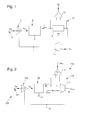
- Some devices such as radio tuners are only equipped with a receiver electronic circuit that is to say having a receiving loop as visible in the figure 1 .
- the receiving loop is also provided with a differential amplifier 11 whose negative input is connected at the output of the peak detector stage, the positive input allowing a reference signal to be compared to the output of the peak detector stage.
- This differential amplifier provides a signal connected to the first amplifier stage to act on it and change its gain.
- a disadvantage of this circuit is that the envelope detector stage, the peak detector stage and the connection track between the output of the differential amplifier and the first amplifier stage are equipped with capacitors of high value.
- these capacitors of high value have the first disadvantage of being expensive. Indeed, capacitors of high value, that is to say the capacitors whose value reaches or exceeds the microfarad are made in expensive technologies and their multiplication thus increases the cost of the circuit.
- these capacitors are generally larger in size, which results in a printed circuit board with a larger surface area and therefore a cost which also increases.
- this receiver circuit has the disadvantage of being complex because the combination of an envelope detector stage and a peak detector stage is not simple.
- the object of the invention is to overcome the drawbacks of the prior art by providing a cheaper receiver system with improved reliability and stability.
- a comparator circuit connected by a positive input to the output of the envelope detector stage and a negative input to the positive input of the second amplifier stage to compare the output of the envelope detector stage to the signal of the amplifier. reference and provide a demodulated output signal.
- An advantage of this receiver circuit is to limit the number of components since the use of a peak detector is not necessary. As a result, the high value capacitor associated with the peak detector circuit is also not used. This allows a saving of printed circuit surface but also a saving in terms of cost because these components represent significant expenses.
- capacitors of high value make it possible to have a better sensitivity of the receiver circuit. Indeed, capacitors of high value are known to cause the appearance of disturbances which deteriorates the sensitivity.
- the envelope detector stage further comprises a protective capacitance
- the comparator circuit comprises a comparator block making the difference between the output signal of the envelope detector stage and the output signal of the second amplifier stage, and a hysteresis block.
- the hysteresis block comprises two pairs of transistors of the same type each comprising a first transistor and a second transistor, the transistors of the same pair being connected to ground, the gate of the first transistor of the first pair and the gate of the second transistor of the second pair being connected together so as to form a first connection point while the gate of the second transistor of the first pair and the gate of the first transistor of the second pair are connected together so to form a second connection point, said hysteresis block being further arranged such that the drains of the first transistor of the first pair and the second transistor of the second pair are connected to the comparator block, the drains of the second transistor of the first pair and the first transistor of the second pair being respectively connected to the drain of the second transistor of the second pair and to the drain of the first transistor of the first pair.
- the hysteresis block further comprises a programmable part comprising two programming transistors each connected by its drain to the sources of the transistors of one of the two pairs of transistors of the hysteresis block, the sources of these transistors of programming are connected to ground and that the gate of each transistor form a connection point for a programming signal.
- the comparator block (BC) is connected to ground via a first control transistor traversed by a first control current, the hysteresis block being connected to ground via a second control transistor traversed by a second adjustment current, the width of the hysteresis being related to the ratio between the second adjustment current and the first adjustment current.
- the first control transistor and the second control transistor each consist of a plurality of parallel-connected transistor that can each be selectively activated or deactivated and that the ratio between the second control current and the first setting current is set by changing the number of transistors activated for the first control transistor and the second control transistor.
- the comparator block differentiates between the output signal of the envelope detector stage and the reference signal, this difference consisting in averaging the detected signal and comparing this average with the value of the reference signal.
- This receiver circuit 100 includes an input 104 through which a signal is received.
- This signal Vin is a signal containing information that can be both a high frequency signal and a low frequency signal.
- This signal Vin is in the form of an amplitude modulated signal.
- This input 104 is connected to a first input of a first amplifier stage 106.
- This first comparator stage 106 comprises a low noise amplifier 107.
- This low noise amplifier 107 is intended to amplify the received signal to provide a signal. Amplified input Vout.
- the output of the first amplifier stage 106 is connected to an envelope detector stage 108.
- This envelope detector stage 108 is used to demodulate the amplified input signal Vout which is the signal Vin amplified receipt that is to say provide a detected signal Vout1 matching the contours of the amplified input signal.
- This envelope detector stage 108 is also used to extract information on the amplitude of the amplified input signal Vout.
- This stage 108 further comprises a capacitor C1 of high capacity connecting said envelope detector stage to the ground. This capacitor C1 is used for envelope detection and filtering of high frequency signals.
- the output of this envelope detector stage 108 is connected to a second amplifier stage 110 which can also be called a second comparator stage.
- This second amplifier stage 110 comprises a transconductance operational amplifier 111.
- the detected signal Vout1 of the envelope detector stage 108 is connected to the negative input of said transconductance operational amplifier 111.
- the positive input of said transconductance operational amplifier 111 is used so that a reference signal Vswref can be connected to it.
- This reference signal Vswref is in the form of a continuous signal whose voltage value is predetermined.
- the transconductance operational amplifier 111 is used to output a control signal Vcom as a setpoint.
- This control signal Vcom is connected to a second input of the first amplifier stage 106, that is to say to a second input of the low noise amplifier 107.
- This control signal Vcom is intended to act on the low noise amplifier 107 to change its gain so that the demodulation is optimal.
- the transconductance operational amplifier 111 compares the signal Vout1 with a reference signal Vswref.
- the signal Vout1 is transformed by the transconductance operational amplifier 111.
- the transconductance operational amplifier 111 is configured to superimposing the detected signal Vout1 at the output of the envelope detector stage 108 and the reference signal Vswref and calculating the area of the signal Vout1 lying above Vswref and below Vswref. Once these areas are calculated by integration, they are compared with each other. In practice, this calculation consists in averaging the detected signal Vout1 and comparing this average with the value of the signal Vswref ideally, the average value of the detected signal Vout1 must be equal to the value of the signal Vswref.
- the command signal Vcom sent is intended to increase the gain of the first stage.
- the detected signal Vout1 output of the envelope detector stage 108 has a mean value greater than the average value of the reference signal Vswref, then the signal Vcom sent is intended to reduce the gain of said first amplifier stage 106.
- the detected signal Vout1 output of the envelope detector stage 108 has a mean value equal to the average value of the reference signal Vswref then the gain is not changed.
- the gain adjustment of the first amplifier stage 106 is done only with the envelope detector 108 and the operational amplifier with a transducer 111.
- the peak detector circuit which is no longer used is obtained. a more compact circuit, less expensive.
- one less capacitor is used which increases the stability of the system.
- the transconductance operational amplifier 111 further comprises a capacitance C2 of high value connected in parallel with the output of said transconductance operational amplifier 111.
- This capacitor is connected to ground and is used as an integrator to stabilize the capacitor. receiving loop.
- the error is stored at the capacitor C2 and the gain control loop makes a setting to the desired value only when the error is zero which implies that the capacitor C2 will not be loaded or discharged.
- the receiver circuit 100 further comprises a comparator stage 112.
- This comparator stage 112 visible at the figure 3 , provides the output signal of the Vdout system and comprises a slider comparator circuit 113 which comprises a comparator block BC and a hysteresis block BH and is powered by a voltage Vdd, the mass being called Vss.
- the comparator block BC is the block through which the input and the output of the comparator stage 112 are arranged.
- the input of said comparator stage 112 is formed by two input terminals Bin + and Bin- comprising a pair of N-type transistors called M1 and M2.
- the terminal Bin + is connected to the transistor M1 and the terminal Bin- is connected to the transistor M2.
- the terminal Bin + is connected to the output of the envelope detector circuit 108 while the terminal Bin- is connected to the positive input terminal of the transconductance operational amplifier 111, that is to say to the reference signal Swref.
- the gates of these transistors M1 and M2 form the input terminals of the comparator stage 112.
- the comparator block BC further comprises a pair of P type transistor called M5 and M6.
- the drain of the transistor M5 is connected to the drain of the transistor M1 while the drain of the transistor M6 is connected to the drain of the transistor M2.
- the source of the transistors M5 and M6 is connected to the voltage Vdd while the gates of these transistors M5 and M6 are connected together to form a connection point for applying a signal to activate the P-type transistors.
- connection points Bm + and Bm- are arranged between the drains of M1 and M5 and the drains of M2 and M6, two output connection points Bm + and Bm- are arranged. These connection points Bm + and Bm- enter a circuit A2 which amplifies the gain of the comparator stage 112 to obtain two output terminals Bout + and Bout- of the comparator stage 112. The output terminals Bout + and Bout- make it possible to output the output signal Vdout.
- the source of the transistor M1 and the source of the transistor M2 are connected together to the drain of a first N-type control transistor called M11, the latter having its source connected to the ground Vss, a first adjustment current Icmp passing through said transistor M11. .
- the hysteresis block BH comprises a first part composed of two pairs of transistors M7, M8 and M9, M10. Each pair of transistors comprises two N-type transistors. It will be understood that the transistors M7, M8 form a first pair while the transistors M9, M10 form a second pair. The transistors of each pair have their sources connected together and also connected to the drain of the transistor M12.
- This first part of the hysteresis block BH is furthermore arranged to be connected respectively to the connection point Bm- that is to say the connection between the drain of M1 and the drain and M5 and to the connection point Bm + it is ie the connection between the drain of M2 and the drain and M6.
- the drain of the transistor M7 and the drain of the transistor M10 are respectively connected respectively to the connection point Bm- and the connection point Bm +.
- the drains of transistors M8 and M9 are connected so that the drain of M8 is connected to the drain of M10 and the drain of M9 is connected to the drain of M7.
- the gates of the transistors are connected in pairs so that the gates of the transistors M7 and M10 are connected together and the gates of the transistors M8 and M9 are connected together. This arrangement makes it possible to form two connection points which are connected to the outputs Bout + and Bout- of the comparator stage 112.
- the configuration of the first part of the hysteresis block BH makes it possible to obtain a hysteresis function associated with the comparator block BC.
- a conventional comparator circuit provided with a hysteresis function.
- the operation of this circuit consists, in the comparator block BC, to compare the detected signal Vout1 and the reference signal Vswref.
- the hysteresis block BH is used to complete this comparison taking into account the output of said comparator stage 112 and the hysteresis signal.
- the hysteresis block comprises a second programmable part.
- This second part comprises a pair of N type transistor called M3 and M4 whose sources are connected together.
- the drains of transistors M3 and M4 are connected to a second part. Therefore, the source of the transistor M7 is connected to the source of the transistor M8 and the drain of the transistor M3 while the source of the transistor M9 is connected to the source of the transistor M10 and the drain of the transistor M4.
- the sources of the transistors M3 and M4 are connected to the drain of a second control transistor M12, the source of which is connected to the ground Vss, the gate of this transistor M12 being connected to the gate of the transistor M11, a second current of adjustment Ihyst traversing said M12 transistor.
- This configuration allows the transistors M11 and M12 to form a connection point making it possible to apply a signal to activate the N-type transistors.
- the gates of the transistors M3 and M4 each form a connection terminal, respectively Bref + and Brief-, used to modify the hysteresis.
- the width of the hysteresis of this circuit is dependent on the ratio between the current Ihyst linked to M12 and the current Icmp linked to M11.
- This width of the hysteresis can then be controlled by modifying this Ihyst / Icmp ratio.
- the transistors M11 and M12 are each constituted in fact of a multitude of transistors in parallel. This configuration allows the current to be distributed in the different transistors.
- the transistors M11 and M12 each consist of the same number of transistors in parallel.
- the ratio of the Ihyst current to the Icmp current varies.
- connection terminals Bre + and Bref- allow the Ihyst current to be modified and thus to modify the width of the hysteresis as visible in FIG. figure 3 . More precisely, by increasing the voltage applied to the connection point Bre +, the width of the hysteresis is increased, that is to say that the switching is delayed to go from a low level to a high level and the switching to go from a high level to a low level. Conversely, by decreasing the width of the hysteresis, the commutations are closer together. However, this hysteresis makes it possible to reduce the effects of noise on the signals. Consequently, this ability to program the width of the hysteresis makes it possible to adapt the noise reduction according to the signal received or the components used.
Landscapes
- Engineering & Computer Science (AREA)
- Computer Networks & Wireless Communication (AREA)
- Signal Processing (AREA)
- Physics & Mathematics (AREA)
- Nonlinear Science (AREA)
- Power Engineering (AREA)
- Manipulation Of Pulses (AREA)
- Circuits Of Receivers In General (AREA)
- Amplifiers (AREA)
Priority Applications (1)
| Application Number | Priority Date | Filing Date | Title |
|---|---|---|---|
| EP13189123.6A EP2725713B1 (de) | 2012-10-26 | 2013-10-17 | Verbessertes empfängersystem |
Applications Claiming Priority (2)
| Application Number | Priority Date | Filing Date | Title |
|---|---|---|---|
| EP12190222.5A EP2725712A1 (de) | 2012-10-26 | 2012-10-26 | Verbessertes Empfangssystem |
| EP13189123.6A EP2725713B1 (de) | 2012-10-26 | 2013-10-17 | Verbessertes empfängersystem |
Publications (3)
| Publication Number | Publication Date |
|---|---|
| EP2725713A2 true EP2725713A2 (de) | 2014-04-30 |
| EP2725713A3 EP2725713A3 (de) | 2016-10-12 |
| EP2725713B1 EP2725713B1 (de) | 2020-12-30 |
Family
ID=47080371
Family Applications (2)
| Application Number | Title | Priority Date | Filing Date |
|---|---|---|---|
| EP12190222.5A Withdrawn EP2725712A1 (de) | 2012-10-26 | 2012-10-26 | Verbessertes Empfangssystem |
| EP13189123.6A Active EP2725713B1 (de) | 2012-10-26 | 2013-10-17 | Verbessertes empfängersystem |
Family Applications Before (1)
| Application Number | Title | Priority Date | Filing Date |
|---|---|---|---|
| EP12190222.5A Withdrawn EP2725712A1 (de) | 2012-10-26 | 2012-10-26 | Verbessertes Empfangssystem |
Country Status (2)
| Country | Link |
|---|---|
| US (1) | US9325361B2 (de) |
| EP (2) | EP2725712A1 (de) |
Families Citing this family (19)
| Publication number | Priority date | Publication date | Assignee | Title |
|---|---|---|---|---|
| US9077386B1 (en) | 2010-05-20 | 2015-07-07 | Kandou Labs, S.A. | Methods and systems for selection of unions of vector signaling codes for power and pin efficient chip-to-chip communication |
| US9288082B1 (en) | 2010-05-20 | 2016-03-15 | Kandou Labs, S.A. | Circuits for efficient detection of vector signaling codes for chip-to-chip communication using sums of differences |
| TWI517577B (zh) * | 2014-01-28 | 2016-01-11 | 晨星半導體股份有限公司 | 適用於積體電路的輸出電路以及相關之控制方法 |
| US9557760B1 (en) * | 2015-10-28 | 2017-01-31 | Kandou Labs, S.A. | Enhanced phase interpolation circuit |
| WO2017132292A1 (en) | 2016-01-25 | 2017-08-03 | Kandou Labs, S.A. | Voltage sampler driver with enhanced high-frequency gain |
| WO2017185070A1 (en) | 2016-04-22 | 2017-10-26 | Kandou Labs, S.A. | Calibration apparatus and method for sampler with adjustable high frequency gain |
| US10003454B2 (en) | 2016-04-22 | 2018-06-19 | Kandou Labs, S.A. | Sampler with low input kickback |
| US10200218B2 (en) | 2016-10-24 | 2019-02-05 | Kandou Labs, S.A. | Multi-stage sampler with increased gain |
| US10742451B2 (en) | 2018-06-12 | 2020-08-11 | Kandou Labs, S.A. | Passive multi-input comparator for orthogonal codes on a multi-wire bus |
| US10931249B2 (en) | 2018-06-12 | 2021-02-23 | Kandou Labs, S.A. | Amplifier with adjustable high-frequency gain using varactor diodes |
| US11183983B2 (en) | 2018-09-10 | 2021-11-23 | Kandou Labs, S.A. | Programmable continuous time linear equalizer having stabilized high-frequency peaking for controlling operating current of a slicer |
| US10574487B1 (en) | 2019-04-08 | 2020-02-25 | Kandou Labs, S.A. | Sampler offset calibration during operation |
| US10608849B1 (en) | 2019-04-08 | 2020-03-31 | Kandou Labs, S.A. | Variable gain amplifier and sampler offset calibration without clock recovery |
| US10680634B1 (en) | 2019-04-08 | 2020-06-09 | Kandou Labs, S.A. | Dynamic integration time adjustment of a clocked data sampler using a static analog calibration circuit |
| US10721106B1 (en) | 2019-04-08 | 2020-07-21 | Kandou Labs, S.A. | Adaptive continuous time linear equalization and channel bandwidth control |
| US11303484B1 (en) | 2021-04-02 | 2022-04-12 | Kandou Labs SA | Continuous time linear equalization and bandwidth adaptation using asynchronous sampling |
| US11374800B1 (en) | 2021-04-14 | 2022-06-28 | Kandou Labs SA | Continuous time linear equalization and bandwidth adaptation using peak detector |
| US11456708B1 (en) | 2021-04-30 | 2022-09-27 | Kandou Labs SA | Reference generation circuit for maintaining temperature-tracked linearity in amplifier with adjustable high-frequency gain |
| US12355409B2 (en) | 2022-03-24 | 2025-07-08 | Kandou Labs SA | Variable gain amplifier with cross-coupled common mode reduction |
Family Cites Families (7)
| Publication number | Priority date | Publication date | Assignee | Title |
|---|---|---|---|---|
| US4782532A (en) * | 1987-04-15 | 1988-11-01 | Motorola, Inc. | Automatic IF tangent lock control circuit |
| FR2742564B1 (fr) * | 1995-12-18 | 1998-01-09 | Valeo Electronique | Circuit detecteur pour la remise en forme d'un signal numerique transmis par onde radiofrequence modulee en amplitude, ainsi qu'un recepteur et un systeme de telecommande l'incorporant, notamment pour vehicule |
| JP2001292183A (ja) * | 2000-04-06 | 2001-10-19 | Nippon Telegr & Teleph Corp <Ntt> | Ask復調回路 |
| JP4321959B2 (ja) | 2000-10-17 | 2009-08-26 | Okiセミコンダクタ株式会社 | 信号補償回路及び復調回路 |
| US7231152B2 (en) * | 2002-04-08 | 2007-06-12 | Silicon Communications Technology Co., Ltd. | Infrared remote control receiver (IRCR) having semiconductor signal processing device therein |
| US8000671B2 (en) * | 2008-04-01 | 2011-08-16 | Seiko Epson Corporation | Dual threshold demodulation in an amplitude modulation radio receiver |
| CN102185646B (zh) * | 2011-05-26 | 2014-09-10 | 泉芯电子技术(深圳)有限公司 | 红外接收器 |
-
2012
- 2012-10-26 EP EP12190222.5A patent/EP2725712A1/de not_active Withdrawn
-
2013
- 2013-10-17 EP EP13189123.6A patent/EP2725713B1/de active Active
- 2013-10-24 US US14/062,355 patent/US9325361B2/en active Active
Non-Patent Citations (1)
| Title |
|---|
| None |
Also Published As
| Publication number | Publication date |
|---|---|
| US9325361B2 (en) | 2016-04-26 |
| US20140119479A1 (en) | 2014-05-01 |
| EP2725713A3 (de) | 2016-10-12 |
| EP2725712A1 (de) | 2014-04-30 |
| EP2725713B1 (de) | 2020-12-30 |
Similar Documents
| Publication | Publication Date | Title |
|---|---|---|
| EP2725713B1 (de) | Verbessertes empfängersystem | |
| EP1424776B1 (de) | Spannungsgesteuerte Oszillatorschaltung für eine elektronische Vorrichtung mit niedriger Leistung | |
| CN113109619B (zh) | 一种接收机解调器、峰值检测器及信号解调方法 | |
| FR2819064A1 (fr) | Regulateur de tension a stabilite amelioree | |
| CA3013842C (fr) | Circuit de detection d'impulsions lumineuses | |
| FR2667744A1 (fr) | Amplificateur operationnel a entrees et sorties differentielles. | |
| EP0856942B1 (de) | Radioempfänger mit Detektor für Unterführungen | |
| EP1873905A1 (de) | Verstärker-Mischer und Empfänger mit einem solchen Verstärker-Mischer | |
| FR2651389A1 (fr) | Amplificateur differentiel a couplage capacitif. | |
| EP3082072A1 (de) | Empfangsblock eines rfid-tags | |
| FR2716052A1 (fr) | Dispositif d'ajustement d'une fréquence de coupure d'un filtre, et filtre comportant un tel dispositif. | |
| EP0271938B1 (de) | Automatische Verstärkungsregelung einer Verstärkerschaltung | |
| EP2725709A1 (de) | Elektronischer Schaltkreis für die automatische Steuerung der Doppelrampenverstärkung eines Verstärkers | |
| EP1916762A1 (de) | Quarzoszillator mit Amplitudenregelung und einem erweiterten Temperaturbereich | |
| FR2882873A1 (fr) | Amplificateur large bande a gain variable | |
| CH707127A2 (fr) | Système récepteur amélioré. | |
| FR3042876A1 (fr) | Detection de perturbations d'une alimentation | |
| EP2705605B1 (de) | Verstärkerschaltung und empfangskette | |
| EP1352302A1 (de) | Spannungsregler mit reduzierter statischen verstärkung in offenem regelkreis | |
| FR2500969A1 (fr) | Amplificateur lineaire et circuit amplificateur a commande de gain comportant au moins un tel amplificateur | |
| FR2785107A1 (fr) | Amplificateur de courant a faible impedance d'entree | |
| EP1246357A2 (de) | Verstärkervorrichtung mit geschalteter Verstärkung insbesondere für ein mobiles Zelltelephon | |
| WO2002007320A1 (fr) | Procede et dispositif de conversion analogique/numerique | |
| FR2892872A1 (fr) | Filtre passe-bande complexe | |
| FR2481541A1 (fr) | Amplificateur a gain regle et a contre-reaction d'emetteur variable |
Legal Events
| Date | Code | Title | Description |
|---|---|---|---|
| PUAI | Public reference made under article 153(3) epc to a published international application that has entered the european phase |
Free format text: ORIGINAL CODE: 0009012 |
|
| 17P | Request for examination filed |
Effective date: 20131017 |
|
| AK | Designated contracting states |
Kind code of ref document: A2 Designated state(s): AL AT BE BG CH CY CZ DE DK EE ES FI FR GB GR HR HU IE IS IT LI LT LU LV MC MK MT NL NO PL PT RO RS SE SI SK SM TR |
|
| AX | Request for extension of the european patent |
Extension state: BA ME |
|
| PUAL | Search report despatched |
Free format text: ORIGINAL CODE: 0009013 |
|
| RIC1 | Information provided on ipc code assigned before grant |
Ipc: H03D 1/10 20060101ALI20160901BHEP Ipc: H03K 5/007 20060101ALI20160901BHEP Ipc: H04L 27/08 20060101ALI20160901BHEP Ipc: H03G 3/30 20060101AFI20160901BHEP |
|
| AK | Designated contracting states |
Kind code of ref document: A3 Designated state(s): AL AT BE BG CH CY CZ DE DK EE ES FI FR GB GR HR HU IE IS IT LI LT LU LV MC MK MT NL NO PL PT RO RS SE SI SK SM TR |
|
| AX | Request for extension of the european patent |
Extension state: BA ME |
|
| STAA | Information on the status of an ep patent application or granted ep patent |
Free format text: STATUS: REQUEST FOR EXAMINATION WAS MADE |
|
| 17P | Request for examination filed |
Effective date: 20170412 |
|
| RBV | Designated contracting states (corrected) |
Designated state(s): AL AT BE BG CH CY CZ DE DK EE ES FI FR GB GR HR HU IE IS IT LI LT LU LV MC MK MT NL NO PL PT RO RS SE SI SK SM TR |
|
| STAA | Information on the status of an ep patent application or granted ep patent |
Free format text: STATUS: EXAMINATION IS IN PROGRESS |
|
| 17Q | First examination report despatched |
Effective date: 20190415 |
|
| GRAP | Despatch of communication of intention to grant a patent |
Free format text: ORIGINAL CODE: EPIDOSNIGR1 |
|
| STAA | Information on the status of an ep patent application or granted ep patent |
Free format text: STATUS: GRANT OF PATENT IS INTENDED |
|
| RIC1 | Information provided on ipc code assigned before grant |
Ipc: H03K 9/00 20060101ALI20200930BHEP Ipc: H03G 3/30 20060101AFI20200930BHEP Ipc: H03K 9/02 20060101ALI20200930BHEP Ipc: H04L 27/08 20060101ALI20200930BHEP Ipc: H03D 1/18 20060101ALI20200930BHEP Ipc: H03K 5/007 20060101ALI20200930BHEP Ipc: H03D 1/10 20060101ALI20200930BHEP |
|
| INTG | Intention to grant announced |
Effective date: 20201019 |
|
| GRAS | Grant fee paid |
Free format text: ORIGINAL CODE: EPIDOSNIGR3 |
|
| GRAA | (expected) grant |
Free format text: ORIGINAL CODE: 0009210 |
|
| STAA | Information on the status of an ep patent application or granted ep patent |
Free format text: STATUS: THE PATENT HAS BEEN GRANTED |
|
| AK | Designated contracting states |
Kind code of ref document: B1 Designated state(s): AL AT BE BG CH CY CZ DE DK EE ES FI FR GB GR HR HU IE IS IT LI LT LU LV MC MK MT NL NO PL PT RO RS SE SI SK SM TR |
|
| REG | Reference to a national code |
Ref country code: GB Ref legal event code: FG4D Free format text: NOT ENGLISH |
|
| REG | Reference to a national code |
Ref country code: DE Ref legal event code: R096 Ref document number: 602013074984 Country of ref document: DE |
|
| REG | Reference to a national code |
Ref country code: AT Ref legal event code: REF Ref document number: 1350934 Country of ref document: AT Kind code of ref document: T Effective date: 20210115 Ref country code: CH Ref legal event code: NV Representative=s name: ICB INGENIEURS CONSEILS EN BREVETS SA, CH |
|
| REG | Reference to a national code |
Ref country code: IE Ref legal event code: FG4D Free format text: LANGUAGE OF EP DOCUMENT: FRENCH |
|
| PG25 | Lapsed in a contracting state [announced via postgrant information from national office to epo] |
Ref country code: NO Free format text: LAPSE BECAUSE OF FAILURE TO SUBMIT A TRANSLATION OF THE DESCRIPTION OR TO PAY THE FEE WITHIN THE PRESCRIBED TIME-LIMIT Effective date: 20210330 Ref country code: RS Free format text: LAPSE BECAUSE OF FAILURE TO SUBMIT A TRANSLATION OF THE DESCRIPTION OR TO PAY THE FEE WITHIN THE PRESCRIBED TIME-LIMIT Effective date: 20201230 Ref country code: FI Free format text: LAPSE BECAUSE OF FAILURE TO SUBMIT A TRANSLATION OF THE DESCRIPTION OR TO PAY THE FEE WITHIN THE PRESCRIBED TIME-LIMIT Effective date: 20201230 Ref country code: GR Free format text: LAPSE BECAUSE OF FAILURE TO SUBMIT A TRANSLATION OF THE DESCRIPTION OR TO PAY THE FEE WITHIN THE PRESCRIBED TIME-LIMIT Effective date: 20210331 |
|
| REG | Reference to a national code |
Ref country code: AT Ref legal event code: MK05 Ref document number: 1350934 Country of ref document: AT Kind code of ref document: T Effective date: 20201230 |
|
| PG25 | Lapsed in a contracting state [announced via postgrant information from national office to epo] |
Ref country code: SE Free format text: LAPSE BECAUSE OF FAILURE TO SUBMIT A TRANSLATION OF THE DESCRIPTION OR TO PAY THE FEE WITHIN THE PRESCRIBED TIME-LIMIT Effective date: 20201230 Ref country code: LV Free format text: LAPSE BECAUSE OF FAILURE TO SUBMIT A TRANSLATION OF THE DESCRIPTION OR TO PAY THE FEE WITHIN THE PRESCRIBED TIME-LIMIT Effective date: 20201230 Ref country code: BG Free format text: LAPSE BECAUSE OF FAILURE TO SUBMIT A TRANSLATION OF THE DESCRIPTION OR TO PAY THE FEE WITHIN THE PRESCRIBED TIME-LIMIT Effective date: 20210330 |
|
| REG | Reference to a national code |
Ref country code: NL Ref legal event code: MP Effective date: 20201230 |
|
| PG25 | Lapsed in a contracting state [announced via postgrant information from national office to epo] |
Ref country code: HR Free format text: LAPSE BECAUSE OF FAILURE TO SUBMIT A TRANSLATION OF THE DESCRIPTION OR TO PAY THE FEE WITHIN THE PRESCRIBED TIME-LIMIT Effective date: 20201230 |
|
| REG | Reference to a national code |
Ref country code: LT Ref legal event code: MG9D |
|
| PG25 | Lapsed in a contracting state [announced via postgrant information from national office to epo] |
Ref country code: LT Free format text: LAPSE BECAUSE OF FAILURE TO SUBMIT A TRANSLATION OF THE DESCRIPTION OR TO PAY THE FEE WITHIN THE PRESCRIBED TIME-LIMIT Effective date: 20201230 Ref country code: SK Free format text: LAPSE BECAUSE OF FAILURE TO SUBMIT A TRANSLATION OF THE DESCRIPTION OR TO PAY THE FEE WITHIN THE PRESCRIBED TIME-LIMIT Effective date: 20201230 Ref country code: RO Free format text: LAPSE BECAUSE OF FAILURE TO SUBMIT A TRANSLATION OF THE DESCRIPTION OR TO PAY THE FEE WITHIN THE PRESCRIBED TIME-LIMIT Effective date: 20201230 Ref country code: PT Free format text: LAPSE BECAUSE OF FAILURE TO SUBMIT A TRANSLATION OF THE DESCRIPTION OR TO PAY THE FEE WITHIN THE PRESCRIBED TIME-LIMIT Effective date: 20210430 Ref country code: CZ Free format text: LAPSE BECAUSE OF FAILURE TO SUBMIT A TRANSLATION OF THE DESCRIPTION OR TO PAY THE FEE WITHIN THE PRESCRIBED TIME-LIMIT Effective date: 20201230 Ref country code: EE Free format text: LAPSE BECAUSE OF FAILURE TO SUBMIT A TRANSLATION OF THE DESCRIPTION OR TO PAY THE FEE WITHIN THE PRESCRIBED TIME-LIMIT Effective date: 20201230 Ref country code: NL Free format text: LAPSE BECAUSE OF FAILURE TO SUBMIT A TRANSLATION OF THE DESCRIPTION OR TO PAY THE FEE WITHIN THE PRESCRIBED TIME-LIMIT Effective date: 20201230 |
|
| PG25 | Lapsed in a contracting state [announced via postgrant information from national office to epo] |
Ref country code: AT Free format text: LAPSE BECAUSE OF FAILURE TO SUBMIT A TRANSLATION OF THE DESCRIPTION OR TO PAY THE FEE WITHIN THE PRESCRIBED TIME-LIMIT Effective date: 20201230 Ref country code: PL Free format text: LAPSE BECAUSE OF FAILURE TO SUBMIT A TRANSLATION OF THE DESCRIPTION OR TO PAY THE FEE WITHIN THE PRESCRIBED TIME-LIMIT Effective date: 20201230 |
|
| PG25 | Lapsed in a contracting state [announced via postgrant information from national office to epo] |
Ref country code: IS Free format text: LAPSE BECAUSE OF FAILURE TO SUBMIT A TRANSLATION OF THE DESCRIPTION OR TO PAY THE FEE WITHIN THE PRESCRIBED TIME-LIMIT Effective date: 20210430 |
|
| REG | Reference to a national code |
Ref country code: DE Ref legal event code: R097 Ref document number: 602013074984 Country of ref document: DE |
|
| PG25 | Lapsed in a contracting state [announced via postgrant information from national office to epo] |
Ref country code: IT Free format text: LAPSE BECAUSE OF FAILURE TO SUBMIT A TRANSLATION OF THE DESCRIPTION OR TO PAY THE FEE WITHIN THE PRESCRIBED TIME-LIMIT Effective date: 20201230 Ref country code: AL Free format text: LAPSE BECAUSE OF FAILURE TO SUBMIT A TRANSLATION OF THE DESCRIPTION OR TO PAY THE FEE WITHIN THE PRESCRIBED TIME-LIMIT Effective date: 20201230 |
|
| PLBE | No opposition filed within time limit |
Free format text: ORIGINAL CODE: 0009261 |
|
| STAA | Information on the status of an ep patent application or granted ep patent |
Free format text: STATUS: NO OPPOSITION FILED WITHIN TIME LIMIT |
|
| PG25 | Lapsed in a contracting state [announced via postgrant information from national office to epo] |
Ref country code: DK Free format text: LAPSE BECAUSE OF FAILURE TO SUBMIT A TRANSLATION OF THE DESCRIPTION OR TO PAY THE FEE WITHIN THE PRESCRIBED TIME-LIMIT Effective date: 20201230 Ref country code: ES Free format text: LAPSE BECAUSE OF FAILURE TO SUBMIT A TRANSLATION OF THE DESCRIPTION OR TO PAY THE FEE WITHIN THE PRESCRIBED TIME-LIMIT Effective date: 20201230 |
|
| 26N | No opposition filed |
Effective date: 20211001 |
|
| PG25 | Lapsed in a contracting state [announced via postgrant information from national office to epo] |
Ref country code: SI Free format text: LAPSE BECAUSE OF FAILURE TO SUBMIT A TRANSLATION OF THE DESCRIPTION OR TO PAY THE FEE WITHIN THE PRESCRIBED TIME-LIMIT Effective date: 20201230 |
|
| PG25 | Lapsed in a contracting state [announced via postgrant information from national office to epo] |
Ref country code: IS Free format text: LAPSE BECAUSE OF FAILURE TO SUBMIT A TRANSLATION OF THE DESCRIPTION OR TO PAY THE FEE WITHIN THE PRESCRIBED TIME-LIMIT Effective date: 20210430 |
|
| REG | Reference to a national code |
Ref country code: BE Ref legal event code: MM Effective date: 20211031 |
|
| GBPC | Gb: european patent ceased through non-payment of renewal fee |
Effective date: 20211017 |
|
| PG25 | Lapsed in a contracting state [announced via postgrant information from national office to epo] |
Ref country code: MC Free format text: LAPSE BECAUSE OF FAILURE TO SUBMIT A TRANSLATION OF THE DESCRIPTION OR TO PAY THE FEE WITHIN THE PRESCRIBED TIME-LIMIT Effective date: 20201230 |
|
| PG25 | Lapsed in a contracting state [announced via postgrant information from national office to epo] |
Ref country code: LU Free format text: LAPSE BECAUSE OF NON-PAYMENT OF DUE FEES Effective date: 20211017 Ref country code: GB Free format text: LAPSE BECAUSE OF NON-PAYMENT OF DUE FEES Effective date: 20211017 Ref country code: BE Free format text: LAPSE BECAUSE OF NON-PAYMENT OF DUE FEES Effective date: 20211031 |
|
| PG25 | Lapsed in a contracting state [announced via postgrant information from national office to epo] |
Ref country code: IE Free format text: LAPSE BECAUSE OF NON-PAYMENT OF DUE FEES Effective date: 20211017 |
|
| PG25 | Lapsed in a contracting state [announced via postgrant information from national office to epo] |
Ref country code: HU Free format text: LAPSE BECAUSE OF FAILURE TO SUBMIT A TRANSLATION OF THE DESCRIPTION OR TO PAY THE FEE WITHIN THE PRESCRIBED TIME-LIMIT; INVALID AB INITIO Effective date: 20131017 |
|
| PG25 | Lapsed in a contracting state [announced via postgrant information from national office to epo] |
Ref country code: CY Free format text: LAPSE BECAUSE OF FAILURE TO SUBMIT A TRANSLATION OF THE DESCRIPTION OR TO PAY THE FEE WITHIN THE PRESCRIBED TIME-LIMIT Effective date: 20201230 |
|
| P01 | Opt-out of the competence of the unified patent court (upc) registered |
Effective date: 20230611 |
|
| PG25 | Lapsed in a contracting state [announced via postgrant information from national office to epo] |
Ref country code: SM Free format text: LAPSE BECAUSE OF FAILURE TO SUBMIT A TRANSLATION OF THE DESCRIPTION OR TO PAY THE FEE WITHIN THE PRESCRIBED TIME-LIMIT Effective date: 20201230 |
|
| PG25 | Lapsed in a contracting state [announced via postgrant information from national office to epo] |
Ref country code: MK Free format text: LAPSE BECAUSE OF FAILURE TO SUBMIT A TRANSLATION OF THE DESCRIPTION OR TO PAY THE FEE WITHIN THE PRESCRIBED TIME-LIMIT Effective date: 20201230 |
|
| PG25 | Lapsed in a contracting state [announced via postgrant information from national office to epo] |
Ref country code: MT Free format text: LAPSE BECAUSE OF FAILURE TO SUBMIT A TRANSLATION OF THE DESCRIPTION OR TO PAY THE FEE WITHIN THE PRESCRIBED TIME-LIMIT Effective date: 20201230 |
|
| PGFP | Annual fee paid to national office [announced via postgrant information from national office to epo] |
Ref country code: FR Payment date: 20250924 Year of fee payment: 13 |
|
| REG | Reference to a national code |
Ref country code: CH Ref legal event code: U11 Free format text: ST27 STATUS EVENT CODE: U-0-0-U10-U11 (AS PROVIDED BY THE NATIONAL OFFICE) Effective date: 20251101 |
|
| PG25 | Lapsed in a contracting state [announced via postgrant information from national office to epo] |
Ref country code: TR Free format text: LAPSE BECAUSE OF FAILURE TO SUBMIT A TRANSLATION OF THE DESCRIPTION OR TO PAY THE FEE WITHIN THE PRESCRIBED TIME-LIMIT Effective date: 20201230 |
|
| PGFP | Annual fee paid to national office [announced via postgrant information from national office to epo] |
Ref country code: DE Payment date: 20250923 Year of fee payment: 13 |
|
| PGFP | Annual fee paid to national office [announced via postgrant information from national office to epo] |
Ref country code: CH Payment date: 20251101 Year of fee payment: 13 |