EP2713311B1 - Imaging apparatus and medical equipment - Google Patents
Imaging apparatus and medical equipment Download PDFInfo
- Publication number
- EP2713311B1 EP2713311B1 EP13186381.3A EP13186381A EP2713311B1 EP 2713311 B1 EP2713311 B1 EP 2713311B1 EP 13186381 A EP13186381 A EP 13186381A EP 2713311 B1 EP2713311 B1 EP 2713311B1
- Authority
- EP
- European Patent Office
- Prior art keywords
- layer
- light
- transmissive
- section
- reflection layer
- Prior art date
- Legal status (The legal status is an assumption and is not a legal conclusion. Google has not performed a legal analysis and makes no representation as to the accuracy of the status listed.)
- Not-in-force
Links
Images


Classifications
-
- G—PHYSICS
- G06—COMPUTING OR CALCULATING; COUNTING
- G06V—IMAGE OR VIDEO RECOGNITION OR UNDERSTANDING
- G06V40/00—Recognition of biometric, human-related or animal-related patterns in image or video data
- G06V40/10—Human or animal bodies, e.g. vehicle occupants or pedestrians; Body parts, e.g. hands
- G06V40/12—Fingerprints or palmprints
- G06V40/13—Sensors therefor
- G06V40/1318—Sensors therefor using electro-optical elements or layers, e.g. electroluminescent sensing
-
- A—HUMAN NECESSITIES
- A61—MEDICAL OR VETERINARY SCIENCE; HYGIENE
- A61B—DIAGNOSIS; SURGERY; IDENTIFICATION
- A61B5/00—Measuring for diagnostic purposes; Identification of persons
- A61B5/145—Measuring characteristics of blood in vivo, e.g. gas concentration or pH-value ; Measuring characteristics of body fluids or tissues, e.g. interstitial fluid or cerebral tissue
- A61B5/14532—Measuring characteristics of blood in vivo, e.g. gas concentration or pH-value ; Measuring characteristics of body fluids or tissues, e.g. interstitial fluid or cerebral tissue for measuring glucose, e.g. by tissue impedance measurement
-
- A—HUMAN NECESSITIES
- A61—MEDICAL OR VETERINARY SCIENCE; HYGIENE
- A61B—DIAGNOSIS; SURGERY; IDENTIFICATION
- A61B5/00—Measuring for diagnostic purposes; Identification of persons
- A61B5/145—Measuring characteristics of blood in vivo, e.g. gas concentration or pH-value ; Measuring characteristics of body fluids or tissues, e.g. interstitial fluid or cerebral tissue
- A61B5/1455—Measuring characteristics of blood in vivo, e.g. gas concentration or pH-value ; Measuring characteristics of body fluids or tissues, e.g. interstitial fluid or cerebral tissue using optical sensors, e.g. spectral photometrical oximeters
-
- G—PHYSICS
- G02—OPTICS
- G02B—OPTICAL ELEMENTS, SYSTEMS OR APPARATUS
- G02B1/00—Optical elements characterised by the material of which they are made; Optical coatings for optical elements
- G02B1/10—Optical coatings produced by application to, or surface treatment of, optical elements
- G02B1/11—Anti-reflection coatings
-
- G—PHYSICS
- G02—OPTICS
- G02B—OPTICAL ELEMENTS, SYSTEMS OR APPARATUS
- G02B27/00—Optical systems or apparatus not provided for by any of the groups G02B1/00 - G02B26/00, G02B30/00
- G02B27/10—Beam splitting or combining systems
- G02B27/14—Beam splitting or combining systems operating by reflection only
- G02B27/145—Beam splitting or combining systems operating by reflection only having sequential partially reflecting surfaces
-
- G—PHYSICS
- G06—COMPUTING OR CALCULATING; COUNTING
- G06V—IMAGE OR VIDEO RECOGNITION OR UNDERSTANDING
- G06V40/00—Recognition of biometric, human-related or animal-related patterns in image or video data
- G06V40/10—Human or animal bodies, e.g. vehicle occupants or pedestrians; Body parts, e.g. hands
-
- H—ELECTRICITY
- H10—SEMICONDUCTOR DEVICES; ELECTRIC SOLID-STATE DEVICES NOT OTHERWISE PROVIDED FOR
- H10F—INORGANIC SEMICONDUCTOR DEVICES SENSITIVE TO INFRARED RADIATION, LIGHT, ELECTROMAGNETIC RADIATION OF SHORTER WAVELENGTH OR CORPUSCULAR RADIATION
- H10F39/00—Integrated devices, or assemblies of multiple devices, comprising at least one element covered by group H10F30/00, e.g. radiation detectors comprising photodiode arrays
- H10F39/80—Constructional details of image sensors
- H10F39/806—Optical elements or arrangements associated with the image sensors
- H10F39/8067—Reflectors
-
- H—ELECTRICITY
- H10—SEMICONDUCTOR DEVICES; ELECTRIC SOLID-STATE DEVICES NOT OTHERWISE PROVIDED FOR
- H10F—INORGANIC SEMICONDUCTOR DEVICES SENSITIVE TO INFRARED RADIATION, LIGHT, ELECTROMAGNETIC RADIATION OF SHORTER WAVELENGTH OR CORPUSCULAR RADIATION
- H10F55/00—Radiation-sensitive semiconductor devices covered by groups H10F10/00, H10F19/00 or H10F30/00 being structurally associated with electric light sources and electrically or optically coupled thereto
- H10F55/20—Radiation-sensitive semiconductor devices covered by groups H10F10/00, H10F19/00 or H10F30/00 being structurally associated with electric light sources and electrically or optically coupled thereto wherein the electric light source controls the radiation-sensitive semiconductor devices, e.g. optocouplers
- H10F55/25—Radiation-sensitive semiconductor devices covered by groups H10F10/00, H10F19/00 or H10F30/00 being structurally associated with electric light sources and electrically or optically coupled thereto wherein the electric light source controls the radiation-sensitive semiconductor devices, e.g. optocouplers wherein the radiation-sensitive devices and the electric light source are all semiconductor devices
- H10F55/255—Radiation-sensitive semiconductor devices covered by groups H10F10/00, H10F19/00 or H10F30/00 being structurally associated with electric light sources and electrically or optically coupled thereto wherein the electric light source controls the radiation-sensitive semiconductor devices, e.g. optocouplers wherein the radiation-sensitive devices and the electric light source are all semiconductor devices formed in, or on, a common substrate
-
- A—HUMAN NECESSITIES
- A61—MEDICAL OR VETERINARY SCIENCE; HYGIENE
- A61B—DIAGNOSIS; SURGERY; IDENTIFICATION
- A61B10/00—Instruments for taking body samples for diagnostic purposes; Other methods or instruments for diagnosis, e.g. for vaccination diagnosis, sex determination or ovulation-period determination; Throat striking implements
- A61B2010/0009—Testing for drug or alcohol abuse
-
- G—PHYSICS
- G06—COMPUTING OR CALCULATING; COUNTING
- G06V—IMAGE OR VIDEO RECOGNITION OR UNDERSTANDING
- G06V40/00—Recognition of biometric, human-related or animal-related patterns in image or video data
- G06V40/10—Human or animal bodies, e.g. vehicle occupants or pedestrians; Body parts, e.g. hands
- G06V40/14—Vascular patterns
Definitions
- the present invention relates to an imaging apparatus which images a subject.
- Patent Document 1 discloses a finger authentication apparatus where a light source section and an imaging section are arranged so as to face each other interposing a subject (a finger of the person to be authenticated) and light which has been emitted from the light source section and passed through a subject is imaged by the imaging section.
- Patent Document 2 discloses an imaging apparatus with a structure where a light source layer and a detection layer are laminated on a surface of a substrate. Light which has been emitted from the light source layer and passed through a subject is detected by each light receiving element in the detection layer.
- Patent Document 1 Japanese Laid-open Patent Publication No. 2003-30632
- Patent Document 2 Japanese Laid-open Patent Publication No. 2009-3821
- JP H05 236200 A discloses a light source integral type image sensor
- US 2011/025899 A1 discloses an array of microlenses with integrated illumination
- US 7 102 282 B1 discloses a display device with a cavity structure for resonating light.
- the advantage of the invention is to take an image of a subject by suppressing glares or shadows.
- an imaging apparatus of the invention is provided with a light receiving section in which a plurality of light receiving elements is arranged, and a light source section arranged in a subject side of the light receiving section and including a light emitting section that emits light toward the subject and a plurality of transmissive sections where the incident light from the subject side is transmitted to each light receiving element side.
- the light emitting section includes a first translucent layer having light permeability, which includes a light emitting layer, a semi-transmissive reflection layer located in the subject side of the first translucent layer, and a reflection layer, which is opposed to the semi-transmissive reflection layer interposing the first translucent layer.
- a resonation structure is formed so that the light emitted from the light emitting layer is resonated between the semi-transmissive reflection layer and the reflection layer.
- the plurality of the transmissive sections respectively includes a second translucent layer having light permeability, and a first semi-transmissive reflection layer and a second semi-transmissive reflection layer that are opposed each other interposing the second translucent layer.
- a resonation structure is formed so that the irradiation light from the light emitting layer is resonated between the first semi-transmissive reflection layer and the second semi-transmissive reflection layer.
- a first resonant length (e.g., resonant length L1) between the reflection layer and the semi-transmissive reflection layer in the light emitting section is more than a second resonance length (e.g., resonant length L2) between the first semi-transmissive reflection layer and the second semi-transmissive reflection layer in the transmissive section.
- the first resonant length of the resonant structure of the light emitting section is more than the second resonant length of the resonant structure of the transmissive section so as to approach between a peak wavelength (e.g., peak wavelength ⁇ 1) of the irradiation intensity from the light emitting section in a direction inclined with respect to a reference direction, which is perpendicular to the reflection surface of the resonant structure, and a peak wavelength (e.g., peak wavelength ⁇ 2) of the irradiation intensity from the transmissive section with respect to the reference direction in comparison with the case that the first resonant length and the second resonant length are matched each other.
- a peak wavelength e.g., peak wavelength ⁇ 1
- peak wavelength ⁇ 2 peak wavelength
- an imaging light in a specific wavelength is emitted from the light emitting section in a direction inclined with respect to the reference direction and passes through the transmissive section in a direction parallel to the reference direction so that it progresses to the light receiving section side. Therefore, it is possible to take a fine and clear image of the subject by suppressing glares or shadows on the surface of the subject.
- the first resonant length and the second resonant length are set so as to match between the peak wavelength (e.g., peak wavelength ⁇ 1) of the irradiation intensity from the light emitting section in the direction inclined with respect to the reference direction and the peak wavelength (e.g., peak wavelength ⁇ 2) of the irradiation intensity from the transmissive section with respect to the reference direction.
- peak wavelength e.g., peak wavelength ⁇ 1
- peak wavelength ⁇ 2 peak wavelength of the irradiation intensity from the transmissive section with respect to the reference direction.
- the phrase "the peak wavelength of the irradiation intensity from the light emitting section and the peak wavelength of the irradiation intensity from the transmissive section are matched” means that in addition to the case that each peak wavelength is totally matched, it includes the case that each peak wavelength is substantively matched (for example, in a case that their difference is within a range of manufacturing error).
- the imaging apparatus is provided with a plurality of lenses which is arranged in the subject side of the light source section so that the incident light from the subject side is focused to each of the light receiving elements.
- the plurality of lenses s arranged so that the incident light from the subject side is focused to each of the light receiving elements.
- an angle in an irradiation direction with respect to a reference direction is more than or equal to 30° and less than or equal to 60° (for example, 45°). According to the configuration described above, it is possible to suppress glares or shadows while the use efficiency of the incident light from the light emitting section maintains in a high level.
- the reflection layer of the light emitting section includes a basic reflection layer having light reflectivity, and a dielectric multilayer film.
- the first semi-transmissive reflection layer of the transmissive section includes the dielectric multilayer film and it does not include the basic reflection layer.
- the dielectric multilayer film of the reflection layer of the light emitting section and the dielectric multilayer film of the first semi-transmissive reflection layer of the transmissive section are formed in the same layer so that it has an advantage that the manufacturing process is simplified in comparison with the case that the reflection layer of the light emitting section and the first semi-transmissive reflection layer of the transmissive section are formed independently of each other.
- the dielectric multilayer film includes a layer formed by amorphous silicon, visible light is blocked by the layer of the amorphous silicon so that it has an advantage that it is not necessary to independently provide an optical filter that blocks the visible light.
- the semi-transmissive reflection layer of the light emitting section and the second semi-transmissive reflection layer of the transmissive section are formed in the same process and are formed by a material having light reflectivity.
- the semi-transmissive reflection layer and the second semi-transmissive reflection layer of the transmissive section are formed in the same process so that it has an advantage that the manufacturing process is simplified in comparison with the case that the semi-transmissive reflection layer and the second transmissive reflection layer are formed independently of each other.
- a reflection conductive layer used as the semi-transmissive reflection layer and the second transmissive reflection layer is formed by the mixture of, for example, magnesium and silver. It is particularly preferable that the ratio of silver is more than the ratio of magnesium.
- the first translucent layer of the light emitting section includes a transparent electrode layer, which has light permeability, and light emitting layer.
- the second translucent layer of the transmissive section includes the light emitting layer and does not include the transparent electrode layer.
- the imaging apparatus is preferably used in various types of electronic equipment.
- the electronic equipment include a biometric authentication apparatus which executes biometric authentication using an image of veins which has been imaged by the imaging apparatus, and a medical equipment (a biometric information estimating apparatus such as a blood alcohol concentration estimating apparatus, a blood sugar level estimating apparatus, and the like) which estimates biometric information for blood alcohol concentration, blood sugar level, and the like from images which have been imaged by the imaging apparatus.
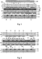
- Fig. 1 is a cross-sectional diagram of an imaging apparatus 100 according to one embodiment of the invention.
- Fig. 2 is an exploded cross-sectional diagram of the imaging apparatus 100.
- the imaging apparatus 100 of the present embodiment is a sensing apparatus which images a subject 200 in a state in which illumination light with a specific wavelength (referred to below as “imaging light”) is irradiated, and for example, is preferably used as a biometric authentication apparatus (vein sensor) which images an image of veins in a living body (typically, a human finger).
- the imaging light is a predetermined frequency of an optic element where the intensity becomes a peak near a specific wavelength ⁇ (hereinafter referred to as "imaging wavelength"). It gives an example that the imaging wavelength ⁇ is 850 nm of near-infrared light below, but the imaging wavelength can be appropriately changed in response to the optical properties (transmittance or reflectance), and the like.
- the imaging apparatus 100 of the invention is provided with a light receiving section 10, light focusing section 20, and a light emitting section 30.
- the light emitting section 30 is arranged in a subject 200 side of the light receiving section 10 (between the light receiving section 10 and the subject 200), and the light focusing section 20 is arranged in the subject 200 side of the light emitting section 30 (between the light emitting section 30 and the subject 200). That is, the light emitting section 30 is located between the light receiving section 10 and the light focusing section 20.
- the incident light from the subject 200 that was illuminated by imaging light emitted from the light emitting section 30 is focused in the light focusing section 20 and passes through the light emitting section 30 and reaches to the light receiving section 10.
- the light receiving section 10 is an element that images the subject 200 and is configured to include a substrate 12 and a plurality of light receiving elements 14.
- the substrate 12 is a member with a plate shape which is formed from, for example, a semiconductor material.
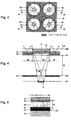
- the plurality of light receiving elements 14 are formed on a surface (acceptance surface) 121 on the subject 200 side of the substrate 12, and are ordered in a matrix formation in a planar view (that is, when viewed from a direction which is perpendicular to the surface 121) as shown in Fig. 3 .
- Each of the plurality of light receiving elements 14 generates a detection signal according to the amount of imaging light.
- An image of the subject 200 is generated by an image processing of the detection signal that was generated in each of the plurality of light receiving elements 14.
- CMOS Complementary Metal Oxide Semiconductor
- CCD Charge Coupled Device
- the light focusing section 20 in Fig. 1 is an element which focuses imaging light that arrives from the subject 200, and is configured to include a substrate 22 and a plurality of lenses (microlenses) 24.
- the substrate 22 is an optically transmissive (a property whereby it is possible for imaging light to pass through) member with a plate shape which includes a surface 221 which opposes the subject 200 and a surface 222 on the opposite side to the surface 221.
- a glass substrate or a quartz substrate is preferably adopted as the substrate 22.
- the plurality of lenses 24 are formed on the surface 222 of the substrate 22.
- Each of the lenses 24 is a convex lens which focuses imaging light which is incident from the subject 200 onto the surface 221 of the substrate 22 and passes through the substrate 22.
- Fig. 4 is a cross-sectional diagram of a part corresponding to one light receiving element 14 in the imaging elements.
- each lens 24 of the light focusing section 20 and each light receiving element 14 of the light receiving section 10 are one to one correspondence.
- a light axis L0 of each lens 24 passes through the light receiving element 14 (typically, a center of a light sensing area of the light receiving element 14) corresponding to the lens 24. Therefore, the plurality of lenses 24 is arranged in matrix formation in a planer view in a similar manner as each light receiving element 14 as shown in Fig. 3 .
- the light emitting section 30 in Fig. 1 has an element that imaging light is generated and the subject 200 is illuminated and the imaging light, which was focused in each lens 24, passes to each light receiving element 14 side, and is configured to include a substrate 32, a light blocking layer 33, a wiring layer 35, a light source section 36, and a protection layer 37.
- the substrate 32 is an optically transmissive member with a plate shape (for example, a glass substrate or a quartz substrate) which includes a surface 321 which opposes the light focusing section 20 (each of the lenses 24) and a surface 322 on the opposite side to the surface 321.
- the light blocking layer 33 is a film body having a light blocking effect (a property to absorb or reflect imaging light) and is formed on the surface 322 of the substrate 32.
- the light blocking layer 33 is formed by a resin material in which a black agent (black pigment) such as, for example, carbon black, and the like is dispersed, or a metal material such as chrome, and the like having the light blocking effect.
- a black agent black pigment
- a metal material such as chrome, and the like having the light blocking effect.
- a plurality of circular-shaped opening sections 34 is formed on the light blocking layer 33.
- Each of the opening sections 34 of the light blocking layer 33 and each of lenses 24 of the light focusing section 20 (or each of the light receiving elements 14 of the light receiving section 10) are one to one correspondence. Specifically, as shown in Fig.
- each of the opening sections 34 is arranged in a matrix formation in a planar view in a similar manner as each of the lenses 24 or each of the light receiving elements 14.
- the wiring layer 35 is formed on the surface 321 of the substrate 32, and is configured to include a wire for supplying electric current to the light source section 36.
- the light source section 36 is formed on the surface of the wiring layer 35, and illuminates the subject 200.
- the imaging light from the subject 200 side passes to each light receiving element 14 side.
- the light source section 36 is separated into a light emitting section 50 and a plurality of transmissive sections 60 in a planer view (that is, it is in a state of viewing in a direction perpendicular to the surface 321 of the substrate 32).
- the light emitting section 50 generates and emits imaging light to illuminate the subject 200.
- the plurality of transmissive sections 60 respectively transmits the incident light from the subject 200 side to each of the light receiving elements 14 side.
- each of the transmissive sections 60 is formed in a circular shape in a planer view.
- Each of the transmissive sections 60 of the light source section 36 and each of the lenses 24 of the light focusing section 20 (or each of the light receiving elements 14 of the light receiving section 10) are one to one correspondence.
- the light axis L0 of each of the lenses 24 passes through the transmissive sections 60 (typically, it passes through a center of the transmissive section 60) corresponding to the lens 24. Therefore, as shown in Fig.
- each of the transmissive sections 60 is arranged in a matrix formation in a planer view in a similar manner as each of the lenses 24 or the light receiving elements 14.
- Each of wirings in the wiring layer 35 is formed in a region overlapping with the light emitting section 50 in a planer view, and it does not overlap with each of the transmissive sections 60.
- the protection layer 37 in Fig. 1 has an element (sealing layer) to protect from external air or fluid by sealing the light source section 36, and it is formed by an insulating material having light permeability (e.g., resin material).
- the light receiving section 10 and the light emitting section 30 are mutually fixed with a space by, for example, an adhesive agent 18 having light permeability. Also, the respective peripheries of the light focusing section 20 and the light emitting section 30 are mutually fixed.
- Fig. 1 and Fig. 4 a configuration that the light focusing section 20 and the light emitting section 30 are connected to contact the surface of each of the lenses 24 of the light focusing section 20 and the surface of the protection section 30 of the light emitting section 30 is exemplified.
- the imaging light which is output from the light emitting section 50 in the light source section 36 passes through the light focusing section 20 (the substrate 22 and each of the lenses 24) and irradiates the subject 200, passes through or is reflected by veins inside the subject 200 and is incident on the light focusing section 20, and passes through the transmissive sections 60 of the light source section 36 and the opening sections 34 in the substrate 32 and the light blocking layer 33 after having been focused by each of the lenses 24 and reaches the light receiving element 14. Accordingly, an image of veins in the subject 200 is imaged.
- the light source section 36 is arranged between each of the light receiving elements 14 in the light receiving section 10 and the subject 200, it is easy to reduce the size of the apparatus in comparison to the technique in Patent Document 1 where a light source section and an imaging section are arranged so as to oppose each other interposing the subject.
- the light emitting section 50 which irradiates imaging light onto the subject 200 is distributed in a planar form, it is possible to reduce uneven distribution of the amount of irradiating light with regard to the subject 200 (to uniformly illuminate the subject 200) in comparison to a case where a point light source such as a Light Emitting Diode (LED), and the like being used to illuminate the subject 200.
- LED Light Emitting Diode
- the imaging light from the subject 200 which is illuminated by the light source section 36 reaches the light receiving element 14 after having been focused by each of the lenses 24 in the light focusing section 20, there is an advantage in that it is possible to secure a sufficient amount of light which reaches from the subject 200 to each of the light receiving elements 14 in comparison to the technique in Patent Document 2 where there is no element which focuses the imaging light.
- Fig. 5 is a cross-sectional diagram that a light emitting section 50 in a light source section 36 is enlarged.
- the light emitting section 50 is configured to include a reflection layer 52, a first translucent layer 54, and a semi-transmissive reflection layer 56.
- the reflection layer 52 is formed on the surface (on the light receiving section 10 side viewed from the first translucent layer 54) of the wiring layer 35
- the first translucent layer 54 is formed on the surface of the reflection layer 52
- the semi-transmissive reflection layer 56 is formed on the surface (on the subject 200 side viewed from the first translucent layer 54) of the first translucent layer 54. That is, the reflection layer 52 and the semi-transmissive reflection layer 56 are opposed each other interposing the first translucent layer 54.
- the first translucent layer 54 is a thin film having light permeability that includes the light emitting layer which generates imaging light.
- the reflection layer 52 is a thin film having light reflectivity so as to reflect the imaging light, which is emitted from the light emitting layer and progresses to the light receiving section 10, to the subject 200 side.
- the semi-transmissive reflection layer 56 is a thin film (half mirror) having semi-transmissive reflectivity so as to transmit a part of the imaging light, which arrives from the first translucent layer 54, (imaging light that the light emitting layer generates and progresses to the subject 200 side, or imaging light reflected in the reflection layer 52) and to reflect the remaining.
- the reflection layer 52 and the semi-transmissive reflection layer 56 are opposed each other interposing the first translucent layer 54 so that the resonation structure (microcavity) that resonates the imaging light, which is emitted from the light emitting layer of the first translucent layer 54, between the reflection layer 52 and the semi-transmissive reflection layer 56. That is, the light emitted from the light emitting layer is reciprocated between the reflection layer 52 and the semi-transmissive reflection layer 56, and passes through the semi-transmissive reflection layer 56 and is emitted to the subject 200 after a resonance component of a wavelength in response to an optical distance L1 (hereinafter referred to as "resonance length") between the reflection layer 52 and the semi-transmissive reflection layer 56 was alternatively amplified.
- resonance length optical distance
- the light emitting section 50 functions as a bandpass filter that alternatively emphasizes a wavelength component in response to the resonance length L1 in the imaging light that the light emitting layer generates.
- the resonance length L1 corresponds to a film thickness of the first translucent layer 54.
- Fig. 6 is a cross-sectional diagram that the transmissive section 60 in the light source section 36 is enlarged.
- the transmissive section 60 is configured to include a first semi-transmissive reflection layer 62, a second translucent layer 64, and a second semi-transmissive reflection layer 66.
- the first semi-transmissive reflection layer 62 is formed on the surface (on the light receiving section 10 side viewed from the second translucent layer 64) of the wiring layer 35
- the second translucent layer 64 is formed on the surface of the first semi-transmissive reflection layer 62
- the second semi-transmissive reflection layer is formed on the surface (on the subject 200 side viewed from the second translucent layer 64) of the second translucent layer 64. That is, the first semi-transmissive reflection layer 62 and the second semi-transmissive reflection layer 66 are opposed each other interposing the second translucent layer 64.
- the second translucent layer 64 is a thin film having light permeability.
- the first semi-transmissive reflection layer 62 is a thin film (half mirror) having semi-transmissive reflectivity so as to pass through a part of the imaging light, which progresses the inside of the second translucent layer 64 to the light receiving section 10 side, to the light receiving section side 10 and reflect the remaining to the subject 200 side (the second semi-transmissive reflection layer 66 side).
- the second semi-transmissive reflection layer 66 is a thin film (half mirror) having semi-transmissive reflectivity so as to transmit a part of the imaging light, which was focused in each of the lenses 24 of the light focusing section 20 and from the subject 200 side, and take it inside of the second translucent layer 64, and reflect a part of the imaging light, which is reflected in the first semi-transmissive reflection layer 62 and progresses to the subject 200 side, to the subject 200 side.
- the first semi-transmissive reflection layer 62 and the second semi-transmissive reflection layer 66 are opposed each other interposing the second translucent layer 64 so as to form a resonant structure that resonates imaging light, which was focused in each of lenses 24 of the light focusing section 20 and from the subject 200, between the first semi-transmissive reflection layer 62 and the second semi-transmissive reflection layer 66.
- the imaging light which arrives from the subject 200 side and transmits through the second semi-transmissive reflection layer 66, is reciprocated between the first semi-transmissive reflection layer 62 and the second semi-transmissive reflection layer 66, and a resonance component of a wavelength in response to a resonance length (optical distance) L2 between the first semi-transmissive reflection layer 62 and the second semi-transmissive reflection layer 66 is alternatively amplified and passes through the first semi-transmissive reflection layer 62 and emits to the light receiving section 10 side.
- the transmissive section 60 functions as a bandpass filter that alternatively emphasizes a wavelength component in response to the resonance length L2.
- the resonance length L2 corresponds to the film thickness of the second translucent layer 64.
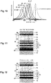
- a relationship between the wavelength and the strength of the irradiation light from the resonance structure depends on an irradiation angle ⁇ of irradiation light.
- the irradiation angle ⁇ means an angle with respect to a reference direction DO perpendicular to the reflection surface of the resonance structure.
- the reference direction D0 is a direction (a direction parallel to a light axis L0 of each of lenses 24 of the light focusing section 20) perpendicular to the surface 121 of the substrate 12.
- ⁇ 0, 15, 30, 45, 60 [°]
- the spectral characteristics of internal luminescence of the light emitting layer are described in a broken line.
- peak wavelength the wavelengths in which the irradiation strength becomes a peak
- the resonance length L1 of the resonance structure of the light emitting section 50 reduces, a peak wavelength of the emitted light tends to be shifted to a short wavelength side.
- the resonance length L1 of the resonance structure of the light emitting section 50 is selected so that a peak wavelength ⁇ 1 of the irradiation strength from the light emitting section 50 in the illumination direction of the target angle ⁇ x matches with (or comes close to) a desired imaging wavelength ⁇ (850 nm). That is, the imaging light of the imaging wavelength ⁇ in the light emitted from the light emitting layer is emitted in the illumination direction that inclines in the target angle ⁇ x with respect to the reference direction D0.
- a case that the target angle ⁇ x was set to 45 ° is exemplified.
- the vertical axis of Fig. 10 can be seen as same as the transmittance of the transmissive section 60.
- Fig. 10 shows a characteristic in the case that the resonance length L2 of the resonance structure of the transmissive section 60 is less than the resonance length L1 of the resonance structure of the light emitting section 50 in a solid line.
- a characteristic for the irradiation angle ⁇ which is 0°, based on a configuration (hereinafter referred to as "comparison example") presuming that the resonance length L1 and the resonance length L2 are matched each other is shown in a broken line.
- Fig. 10 in the similar manner as Fig. 8 , as the irradiation angle ⁇ of the irradiation light from the resonance structure increases, it tends to reduce the peak wavelength of the irradiation light. Also, as is understood from the comparison example of Fig.
- the resonance length L2 of the resonance structure of the transmissive section 60 reduces in comparison to the comparison example (resonance length LI)
- the peak wavelengths of the light emitted from the resonance structure tend to be shifted to the short wavelength side in comparison to the comparison example as shown in Fig. 10 .
- the peak wavelength ⁇ 2 of the irradiation strength (transmittance of the transmissive section 60) from the transmissive section 60 with respect to the reference direction DO (direction of light axis L0 of lenses 24) matches with the imaging wavelength ⁇ .
- the resonance length L2 is selected to be less than the resonance length L1 (L2 ⁇ L1).
- the resonance length L1 and the resonance length L2 are selected to be that the resonance length L1 is 10% (preferably 8%) more than the resonance length L2.
- the resonance length L2 is selected to become approximately one half of the imaging wavelength ⁇ (0.5 wavelength).
- the resonance length L1 and the resonance length L2 are selected as to approach between the peak wavelength ⁇ 1 and the peak wavelength ⁇ 2 in comparison with the comparison example (ideally, both the peak wavelength ⁇ 1 and the peak wavelength ⁇ 2 are matched).
- the imaging light of the desired imaging wavelength ⁇ is emitted from the light emitting section 50 in an illumination direction that inclines the target angle ⁇ x with respect to the reference direction D0, and it passes through the transmissive section 60 in the reference direction DO and progresses to the light receiving section 10 side. Therefore, in the present embodiment, it is possible to take a fine and clear image of the subject 200 while the glares or the shadows of the surface of the subject 200 are suppressed.
- Fig. 11 is a cross-sectional diagram showing a specific configuration of the light emitting section in the light source section 36.
- Fig. 12 is a cross-sectional diagram showing a specific configuration of the transmissive section 60 in the light source section 36.
- the reflection layer 52 of the light emitting section 50 is configured to include a basic reflection layer 71 and a dielectric multilayer film 72 as shown in Fig. 11
- the first semi-transmissive reflection layer 62 of the transmissive section 60 is configured to include the dielectric multilayer film 72 as shown in Fig. 12 .
- the dielectric multilayer film 72 of the light emitting section 50 and the dielectric multilayer film 72 of the transmissive section 60 are formed in the same layer, and the first semi-transmissive reflection layer 62 does not include the basic reflection layer 71. That is, the first semi-transmissive reflection layer 62 of the transmissive section 60 has a relationship that the layers from the reflection layer 52 of the light emitting section 50 to the basic reflection layer 71 are omitted.
- the basic reflection layer 71 in Fig. 11 is a thin film having light permeability, and is formed on the surface (on the surface 321 of the substrate 32) of the wiring layer 35 by a metal material which is, for example, silver, aluminum, or the like. Specifically, the basic reflection layer 71 is formed by alternatively removing the circular area corresponding to each of the transmissive sections 60 in the thin film having light permeability that was formed in the entire area of the substrate 32.
- the dielectric multilayer film 72 in both of the light emitting section 50 and the transmissive section 60 is a dielectric mirror in which a plurality of high refractive index layers 721 and a plurality of low refractive index layers 722 are alternatively laminated.
- the high refractive index layer 721 and the low refractive index layer 722 are a thin film (dielectric layer) having light permeability, and the refraction index of the high refractive index layer 721 is more than the low refractive index layer 722.
- Each of the high refractive index layers is formed by, for example, amorphous silicon (a-Si), and each of the low refractive index layers is formed by, for example, silicone nitride (SiNx) or silicon oxide (SiOx).
- the film thickness of each of the high refractive index layers and each of the low refractive index layers is set to be that the respective optical distances (length of light path) becomes one-quarter of the imaging length ⁇ .
- the reflection layer 52 of the light emitting section 50 was formed by laminating the basic reflection layer 71 and the dielectric multilayer film 72 as exemplified above, it is possible to improve the reflectance (approximately 95%) in comparison with the case that the reflection layer 52 is formed by a single basic reflection layer 71. Also, there is an advantage that the optical loss can be reduced enough by using the dielectric multilayer film 72. By the way, there is a characteristic to absorb visible light in amorphous silicon which is the material of the high refractive index layer 721 so that according to the configuration that the dielectric multilayer film 72 includes the high refractive index layer 721 of amorphous, there is an advantage that it is not necessary to provide an optical filter independently to block the visible light.
- the first translucent layer 54 of the light emitting section 50 is configured to include a protection layer 73, a transparent electrode layer 74, and a light emitting layer 75 as shown in Fig. 11
- the second translucent layer 64 of the transmissive section 60 is configured to include the protection layer 73 and the light emitting layer 75 as shown in Fig. 12 .
- the protection layer 73 of the first translucent layer 54 and the protection layer 73 of the second translucent layer 64 are formed in the same layer, and the light emitting layer 75 of the first translucent layer 54 and the light emitting layer 75 of the second translucent layer 64 are formed in the same layer.
- the second translucent layer 64 does not include the transparent electrode layer 74. That is, the second translucent layer 64 of the transmissive section 60 has a relationship that the layers from the first translucent layer 64 to the transparent electrode layer 74 are omitted.
- the protection layer 73 in both of the light emitting section 50 and the transmissive section 60 is a thin film having light permeability, and for example, silicone nitride (SiNx) or silicon oxide (SiOx) are formed on the surface of the dielectric multilayer film 72 in the similar manner as the low refractive layer 722 of the dielectric multilayer film 72.
- the transparent electrode layer 74 is a conducting layer having light permeability that functions as an electrode (anelectrode) to supply electric current to the light emitting layer 75 in the light emitting section 50.
- the transparent electrode layer 74 is formed by alternatively removing the circular area corresponding to each of the transmissive sections 60 in the conducting film having light permeability that was formed in the entire of the surface of the protection layer 73.
- the transparent electrode layer 74 is electrically connected to the wiring (not shown) of the wiring layer 35 through a conduction hole (not shown) that penetrates through the protection layer 73.
- the light emitting layer 75 in both of the light emitting section 50 and the light transmissive section 60 are an electrooptic layer that generates imaging light by supplying the electric current, and is formed by, for example, an Electroluminescence material (organic EL).
- an Electroluminescence material organic EL
- the light emitting layer 75 is illustrated as a single layer in Fig. 11 and Fig. 12 for descriptive purposes, but it is possible to form a charge injection layer (hole injection layer, electron injection layer) or a charge transport layer (hole transport layer, electron transport layer) to improve luminance efficiency of the light emitting layer 75.
- the semi-transmissive reflection layer 56 of the light emitting section 50 and the second semi-transmissive reflection layer 66 of the transmissive section 60 are formed in the same layer (reflection conductive layer 76).
- the reflection conductive layer 76 of the light emitting section 50 functions as electrode (negative electrode) to supply electric current to the light emitting layer 75. That is, in the light emitting section 50, the transparent electrode layer 74 and the reflection conductive layer 76 are opposed each other interposing the light emitting layer 75 so as to form a light emitting element (top mission type organic EL element).
- the light emitting layer 75 is existed in the transmissive section 60, but the transparent electrode layer 74 is omitted in the transmissive section 60 so that the light emitting element is not formed.
- the reflection conductive layer 76 is formed by an alloy (MgAg) that mixes magnesium (Mg) and silver (Ag). Specifically, from the viewpoint to realize good semi-transmissive reflectivity, the alloy in which the ratio of silver (% by weight) is more than the ratio of magnesium is preferred as a material of the conducting layer.
- the reflection conductive layer 76 is formed in the film thickness from approximately 20 nm to 30 nm with an alloy in which the ratio of the magnesium is less than 10% and the ratio of silver is more than 90%.
- the protection layer 37 is formed on the surface of the reflection conductive layer 76 in both of the light emitting section 50 and the transmissive section 60.
- the resonance length L1 of the resonance structure of the light emitting section 50 corresponds to the distance between the front surface of the dielectric multilayer film 72 (most top layer of the high refractive index layer 721) of the reflection layer 52 and the back surface of the semi-transmissive reflection layer (reflection conductive layer 76). That is, the resonance length L1 of the light emitting section 50 is total value of the film thicknesses of the protection layer 73, the transparent electrode layer 74, and the light emitting layer 75.
- Fig. 11 the resonance length L1 of the resonance structure of the light emitting section 50 corresponds to the distance between the front surface of the dielectric multilayer film 72 (most top layer of the high refractive index layer 721) of the reflection layer 52 and the back surface of the semi-transmissive reflection layer (reflection conductive layer 76). That is, the resonance length L1 of the light emitting section 50 is total value of the film thicknesses of the protection layer 73, the transparent electrode layer 74, and the light emitting layer 75.
- the resonance length L2 of the resonance structure of the transmissive section 60 corresponds to the distance between the front surface of the dielectric multilayer film 72 of the first semi-transmissive reflection layer 62 and the back surface of the second semi-transmissive reflection layer 66. That is, the resonance length L2 of the transmissive section 60 is a total value of the film thicknesses of the protection layer 73 and the light emitting layer 75. As is understood from the description above, the resonance length L2 is less than the resonance length L1 by the film thickness of the transparent electrode layer 74.
- the resonance length L1 of the light emitting section 50 and the resonance length L2 of the transmissive section 60 are differentiated in response to existence or non-existence of a part of layers of configuration (transparent electrode layer 74 in the above example) in the respective resonance structures of the light emitting section 50 and the transmissive section 60 as described above, it is possible to differentiate the resonance length L1 and the resonance length L2 with a simple process in comparison with a configuration that the film thickness of the configured layer itself of the resonance structure in the light emitting section 50 and the transmissive section 60 is differentiated.
Landscapes
- Physics & Mathematics (AREA)
- Engineering & Computer Science (AREA)
- Health & Medical Sciences (AREA)
- Life Sciences & Earth Sciences (AREA)
- General Physics & Mathematics (AREA)
- Optics & Photonics (AREA)
- Human Computer Interaction (AREA)
- Multimedia (AREA)
- Theoretical Computer Science (AREA)
- Biophysics (AREA)
- Veterinary Medicine (AREA)
- Pathology (AREA)
- Biomedical Technology (AREA)
- Heart & Thoracic Surgery (AREA)
- Medical Informatics (AREA)
- Molecular Biology (AREA)
- Surgery (AREA)
- Animal Behavior & Ethology (AREA)
- General Health & Medical Sciences (AREA)
- Public Health (AREA)
- Spectroscopy & Molecular Physics (AREA)
- Emergency Medicine (AREA)
- Measurement Of The Respiration, Hearing Ability, Form, And Blood Characteristics Of Living Organisms (AREA)
- Image Input (AREA)
- Studio Devices (AREA)
- Electroluminescent Light Sources (AREA)
- Transforming Light Signals Into Electric Signals (AREA)
- Stroboscope Apparatuses (AREA)
- Magnetic Resonance Imaging Apparatus (AREA)
Applications Claiming Priority (1)
| Application Number | Priority Date | Filing Date | Title |
|---|---|---|---|
| JP2012219278A JP6044239B2 (ja) | 2012-10-01 | 2012-10-01 | 撮像装置および医療機器 |
Publications (3)
| Publication Number | Publication Date |
|---|---|
| EP2713311A2 EP2713311A2 (en) | 2014-04-02 |
| EP2713311A3 EP2713311A3 (en) | 2016-11-23 |
| EP2713311B1 true EP2713311B1 (en) | 2018-09-05 |
Family
ID=49385102
Family Applications (1)
| Application Number | Title | Priority Date | Filing Date |
|---|---|---|---|
| EP13186381.3A Not-in-force EP2713311B1 (en) | 2012-10-01 | 2013-09-27 | Imaging apparatus and medical equipment |
Country Status (4)
| Country | Link |
|---|---|
| US (3) | US9064768B2 (enExample) |
| EP (1) | EP2713311B1 (enExample) |
| JP (1) | JP6044239B2 (enExample) |
| CN (1) | CN103713448B (enExample) |
Families Citing this family (26)
| Publication number | Priority date | Publication date | Assignee | Title |
|---|---|---|---|---|
| JP6044239B2 (ja) * | 2012-10-01 | 2016-12-14 | セイコーエプソン株式会社 | 撮像装置および医療機器 |
| US10460188B2 (en) * | 2014-08-26 | 2019-10-29 | Gingy Technology Inc. | Bio-sensing apparatus |
| JP2016115862A (ja) * | 2014-12-17 | 2016-06-23 | セイコーエプソン株式会社 | 画像取得装置、生体情報取得装置、電子機器 |
| JP6507670B2 (ja) * | 2015-01-27 | 2019-05-08 | セイコーエプソン株式会社 | 情報取得機器 |
| JP2016225814A (ja) * | 2015-05-29 | 2016-12-28 | セイコーエプソン株式会社 | 撮像装置、撮像装置の制御方法 |
| CN106407881B (zh) * | 2015-07-29 | 2020-07-31 | 财团法人工业技术研究院 | 生物辨识装置及方法与穿戴式载体 |
| US10679081B2 (en) * | 2015-07-29 | 2020-06-09 | Industrial Technology Research Institute | Biometric device and wearable carrier |
| US10853465B2 (en) * | 2015-12-08 | 2020-12-01 | Merck Patent Gmbh | Optical fingerprint authentication device |
| CN107451518A (zh) * | 2016-05-30 | 2017-12-08 | 深圳印象认知技术有限公司 | 一种显示屏 |
| CN206541281U (zh) * | 2016-10-12 | 2017-10-03 | 肖特玻璃科技(苏州)有限公司 | 一种电子器件结构及其使用的超薄玻璃板 |
| CN110192430B (zh) * | 2017-01-18 | 2021-10-01 | 日本先锋公司 | 光装置 |
| WO2018173825A1 (ja) * | 2017-03-21 | 2018-09-27 | パイオニア株式会社 | 光装置 |
| CN109411504B (zh) * | 2017-08-16 | 2021-07-13 | 固安翌光科技有限公司 | 用作指纹识别装置光源的oled屏体及光学指纹识别装置 |
| CN107644202B (zh) * | 2017-09-08 | 2021-01-08 | 维沃移动通信有限公司 | 一种光学指纹模组及移动终端 |
| CN110097821A (zh) * | 2018-01-30 | 2019-08-06 | 华为技术有限公司 | 屏幕模组和配置屏幕模组的电子设备 |
| CN108647598B (zh) * | 2018-04-27 | 2021-06-01 | 上海天马有机发光显示技术有限公司 | 一种显示面板和显示装置 |
| US11215335B2 (en) * | 2018-06-21 | 2022-01-04 | Ichikoh Industries, Ltd. | Light source unit of vehicle lighting system and vehicle lighting system |
| JP7151615B2 (ja) * | 2019-05-09 | 2022-10-12 | セイコーエプソン株式会社 | 有機el表示装置、および電子機器 |
| CN110192843B (zh) * | 2019-05-31 | 2022-04-15 | Oppo广东移动通信有限公司 | 信息推送方法及相关产品 |
| CN110441944B (zh) * | 2019-07-31 | 2022-02-08 | 上海天马微电子有限公司 | 显示面板及显示装置 |
| KR20220098373A (ko) * | 2019-11-08 | 2022-07-12 | 비아비 솔루션즈 아이엔씨. | 광학 코팅 및 광학 코팅을 포함하는 장치 |
| EP4111234A4 (en) | 2020-02-27 | 2023-11-15 | Shenzhen Xpectvision Technology Co., Ltd. | GLYCEMIA RATE DETECTION DEVICE |
| JP7176552B2 (ja) * | 2020-08-31 | 2022-11-22 | セイコーエプソン株式会社 | 電気光学装置および電子機器 |
| CN114005145B (zh) * | 2021-10-27 | 2025-08-15 | 合肥维信诺科技有限公司 | 一种显示面板及显示装置 |
| CN119498830A (zh) * | 2023-08-24 | 2025-02-25 | 广东小天才科技有限公司 | 检测装置及血糖仪 |
| WO2025187520A1 (ja) * | 2024-03-06 | 2025-09-12 | ソニーセミコンダクタソリューションズ株式会社 | 表示装置、表示装置の製造方法および発光素子 |
Family Cites Families (26)
| Publication number | Priority date | Publication date | Assignee | Title |
|---|---|---|---|---|
| JPH05236200A (ja) * | 1992-02-21 | 1993-09-10 | Fuji Xerox Co Ltd | 光源一体型イメ−ジセンサ |
| JP3541416B2 (ja) * | 1994-03-08 | 2004-07-14 | ソニー株式会社 | 光学装置 |
| JP3008859B2 (ja) * | 1996-09-18 | 2000-02-14 | 日本電気株式会社 | 薄型光源を用いたイメージセンサ装置 |
| JP4381517B2 (ja) | 1999-08-11 | 2009-12-09 | セイコーインスツル株式会社 | 指紋読み取り装置及び方法 |
| WO2001039554A1 (fr) * | 1999-11-22 | 2001-05-31 | Sony Corporation | Dispositif d'affichage |
| JP3617476B2 (ja) | 2001-07-19 | 2005-02-02 | 株式会社日立製作所 | 指認証装置 |
| JP4671672B2 (ja) * | 2004-12-01 | 2011-04-20 | 株式会社リコー | 受発光装置、光送受信モジュール、光送信モジュールおよび光通信システム |
| JP4462155B2 (ja) * | 2005-09-27 | 2010-05-12 | セイコーエプソン株式会社 | 発光装置、発光装置の製造方法および電子機器 |
| US7728902B2 (en) | 2006-08-04 | 2010-06-01 | Hitachi Maxell, Ltd. | Imaging device and biometrics authentication apparatus |
| JP5007082B2 (ja) | 2006-08-04 | 2012-08-22 | 日立マクセル株式会社 | 撮像装置および生体認証装置 |
| JP4864632B2 (ja) * | 2006-10-12 | 2012-02-01 | 株式会社リコー | 画像入力装置、画像入力方法、個人認証装置及び電子機器 |
| JP4844481B2 (ja) | 2007-06-25 | 2011-12-28 | 株式会社日立製作所 | 撮像装置及びこれを搭載した装置 |
| KR101434361B1 (ko) * | 2007-10-16 | 2014-08-26 | 삼성디스플레이 주식회사 | 백색 유기 전계 발광소자 및 이를 이용한 컬러 디스플레이장치 |
| DE102007050167A1 (de) * | 2007-10-19 | 2009-04-23 | Fraunhofer-Gesellschaft zur Förderung der angewandten Forschung e.V. | Mikrolinsen-Array mit integrierter Beleuchtung |
| JP5144217B2 (ja) | 2007-10-31 | 2013-02-13 | 株式会社日立製作所 | 撮像装置、撮像装置の製造方法及び撮像装置を搭載した装置 |
| JP2009172263A (ja) | 2008-01-28 | 2009-08-06 | Hitachi Maxell Ltd | 生体情報取得装置及び撮像装置 |
| WO2011114424A1 (ja) * | 2010-03-15 | 2011-09-22 | パイオニア株式会社 | 有機elパネル及びその製造方法 |
| CN102418851B (zh) * | 2010-09-27 | 2014-07-30 | 北京京东方光电科技有限公司 | 发光二极管光源及其制造方法、具有其的背光源 |
| JP5742348B2 (ja) * | 2011-03-23 | 2015-07-01 | セイコーエプソン株式会社 | 撮像装置 |
| JP5712746B2 (ja) | 2011-04-06 | 2015-05-07 | セイコーエプソン株式会社 | センシング装置および電子機器 |
| JP2012222483A (ja) | 2011-04-06 | 2012-11-12 | Seiko Epson Corp | センシング装置および電子機器 |
| JP2012221082A (ja) | 2011-04-06 | 2012-11-12 | Seiko Epson Corp | センシング装置および電子機器 |
| JP2012222484A (ja) | 2011-04-06 | 2012-11-12 | Seiko Epson Corp | センシング装置および電子機器 |
| JP5828371B2 (ja) * | 2011-04-07 | 2015-12-02 | セイコーエプソン株式会社 | 画像取得装置、生体認証装置、電子機器 |
| JP6069822B2 (ja) | 2011-10-12 | 2017-02-01 | セイコーエプソン株式会社 | 撮像方法、生体認証方法、撮像装置および生体認証装置 |
| JP6044239B2 (ja) * | 2012-10-01 | 2016-12-14 | セイコーエプソン株式会社 | 撮像装置および医療機器 |
-
2012
- 2012-10-01 JP JP2012219278A patent/JP6044239B2/ja not_active Expired - Fee Related
-
2013
- 2013-09-27 EP EP13186381.3A patent/EP2713311B1/en not_active Not-in-force
- 2013-09-29 CN CN201310456344.9A patent/CN103713448B/zh not_active Expired - Fee Related
- 2013-09-30 US US14/041,400 patent/US9064768B2/en active Active
-
2015
- 2015-06-15 US US14/739,408 patent/US9405954B2/en active Active
-
2016
- 2016-06-27 US US15/193,563 patent/US20160307058A1/en not_active Abandoned
Non-Patent Citations (1)
| Title |
|---|
| None * |
Also Published As
| Publication number | Publication date |
|---|---|
| US20150310249A1 (en) | 2015-10-29 |
| EP2713311A3 (en) | 2016-11-23 |
| US20140091328A1 (en) | 2014-04-03 |
| US9405954B2 (en) | 2016-08-02 |
| JP2014071800A (ja) | 2014-04-21 |
| US20160307058A1 (en) | 2016-10-20 |
| CN103713448A (zh) | 2014-04-09 |
| CN103713448B (zh) | 2017-11-24 |
| EP2713311A2 (en) | 2014-04-02 |
| US9064768B2 (en) | 2015-06-23 |
| JP6044239B2 (ja) | 2016-12-14 |
Similar Documents
| Publication | Publication Date | Title |
|---|---|---|
| EP2713311B1 (en) | Imaging apparatus and medical equipment | |
| US11048903B2 (en) | Under-LCD screen optical sensor module for on-screen fingerprint sensing | |
| KR102098657B1 (ko) | 디스플레이 일체형 지문센서를 갖는 전자기기, 그것의 사용자 인증 방법, 및 그것의 사용자 지문 등록 방법 | |
| US9543344B2 (en) | Imaging apparatus | |
| JP4844481B2 (ja) | 撮像装置及びこれを搭載した装置 | |
| KR102115546B1 (ko) | 전자기기, 그것의 사용자 인증 방법, 및 그것의 사용자 생체정보 등록 방법 | |
| US11922715B2 (en) | Imaging device | |
| WO2018049944A1 (en) | Under-screen optical sensor module for on-screen fingerprint sensing | |
| US9379157B2 (en) | Image acquisition device, biometric authentication device, and electronic apparatus | |
| EP3461292A1 (en) | Anti-spoofing sensing for rejecting fake fingerprint patterns in under-screen optical sensor module for on-screen fingerprint sensing | |
| KR102762169B1 (ko) | 발광장치, 표시장치, 촬상장치 및 전자기기, 및 발광장치의 제조방법 | |
| CN114730501A (zh) | 包括微透镜的用于红外成像的生物计量成像装置 | |
| WO2020109032A1 (en) | System for optical imaging comprising matched spectral filters | |
| CN105816185B (zh) | 信息取得设备 | |
| CN111902822B (zh) | 利用外部光源的屏下照明 | |
| US20180325427A1 (en) | Imaging device, biometric authentication device, and semiconductor laser | |
| CN112154443B (zh) | 光路折叠的光学指纹感应器 | |
| KR20200054936A (ko) | 전자기기, 그것의 사용자 인증 방법, 및 그것의 사용자 생체정보 등록 방법 | |
| CN213519962U (zh) | 显示装置、检测模组、图像模组和电子设备 | |
| CN213519959U (zh) | 显示装置、检测模组、图像模组和电子设备 | |
| TW201935313A (zh) | 辨識裝置 | |
| JP2014086567A (ja) | 撮像装置 |
Legal Events
| Date | Code | Title | Description |
|---|---|---|---|
| PUAI | Public reference made under article 153(3) epc to a published international application that has entered the european phase |
Free format text: ORIGINAL CODE: 0009012 |
|
| AK | Designated contracting states |
Kind code of ref document: A2 Designated state(s): AL AT BE BG CH CY CZ DE DK EE ES FI FR GB GR HR HU IE IS IT LI LT LU LV MC MK MT NL NO PL PT RO RS SE SI SK SM TR |
|
| AX | Request for extension of the european patent |
Extension state: BA ME |
|
| PUAL | Search report despatched |
Free format text: ORIGINAL CODE: 0009013 |
|
| AK | Designated contracting states |
Kind code of ref document: A3 Designated state(s): AL AT BE BG CH CY CZ DE DK EE ES FI FR GB GR HR HU IE IS IT LI LT LU LV MC MK MT NL NO PL PT RO RS SE SI SK SM TR |
|
| AX | Request for extension of the european patent |
Extension state: BA ME |
|
| RIC1 | Information provided on ipc code assigned before grant |
Ipc: G02B 26/00 20060101ALI20161020BHEP Ipc: G06K 9/20 20060101ALI20161020BHEP Ipc: G02B 5/28 20060101ALI20161020BHEP Ipc: G06K 9/00 20060101AFI20161020BHEP |
|
| 17P | Request for examination filed |
Effective date: 20170424 |
|
| RBV | Designated contracting states (corrected) |
Designated state(s): AL AT BE BG CH CY CZ DE DK EE ES FI FR GB GR HR HU IE IS IT LI LT LU LV MC MK MT NL NO PL PT RO RS SE SI SK SM TR |
|
| GRAP | Despatch of communication of intention to grant a patent |
Free format text: ORIGINAL CODE: EPIDOSNIGR1 |
|
| INTG | Intention to grant announced |
Effective date: 20180509 |
|
| GRAS | Grant fee paid |
Free format text: ORIGINAL CODE: EPIDOSNIGR3 |
|
| GRAA | (expected) grant |
Free format text: ORIGINAL CODE: 0009210 |
|
| AK | Designated contracting states |
Kind code of ref document: B1 Designated state(s): AL AT BE BG CH CY CZ DE DK EE ES FI FR GB GR HR HU IE IS IT LI LT LU LV MC MK MT NL NO PL PT RO RS SE SI SK SM TR |
|
| REG | Reference to a national code |
Ref country code: GB Ref legal event code: FG4D |
|
| REG | Reference to a national code |
Ref country code: CH Ref legal event code: EP |
|
| REG | Reference to a national code |
Ref country code: AT Ref legal event code: REF Ref document number: 1038683 Country of ref document: AT Kind code of ref document: T Effective date: 20180915 |
|
| REG | Reference to a national code |
Ref country code: FR Ref legal event code: PLFP Year of fee payment: 6 |
|
| REG | Reference to a national code |
Ref country code: IE Ref legal event code: FG4D |
|
| REG | Reference to a national code |
Ref country code: DE Ref legal event code: R096 Ref document number: 602013043034 Country of ref document: DE |
|
| REG | Reference to a national code |
Ref country code: NL Ref legal event code: MP Effective date: 20180905 |
|
| REG | Reference to a national code |
Ref country code: LT Ref legal event code: MG4D |
|
| PG25 | Lapsed in a contracting state [announced via postgrant information from national office to epo] |
Ref country code: BG Free format text: LAPSE BECAUSE OF FAILURE TO SUBMIT A TRANSLATION OF THE DESCRIPTION OR TO PAY THE FEE WITHIN THE PRESCRIBED TIME-LIMIT Effective date: 20181205 Ref country code: GR Free format text: LAPSE BECAUSE OF FAILURE TO SUBMIT A TRANSLATION OF THE DESCRIPTION OR TO PAY THE FEE WITHIN THE PRESCRIBED TIME-LIMIT Effective date: 20181206 Ref country code: NO Free format text: LAPSE BECAUSE OF FAILURE TO SUBMIT A TRANSLATION OF THE DESCRIPTION OR TO PAY THE FEE WITHIN THE PRESCRIBED TIME-LIMIT Effective date: 20181205 Ref country code: SE Free format text: LAPSE BECAUSE OF FAILURE TO SUBMIT A TRANSLATION OF THE DESCRIPTION OR TO PAY THE FEE WITHIN THE PRESCRIBED TIME-LIMIT Effective date: 20180905 Ref country code: LT Free format text: LAPSE BECAUSE OF FAILURE TO SUBMIT A TRANSLATION OF THE DESCRIPTION OR TO PAY THE FEE WITHIN THE PRESCRIBED TIME-LIMIT Effective date: 20180905 Ref country code: RS Free format text: LAPSE BECAUSE OF FAILURE TO SUBMIT A TRANSLATION OF THE DESCRIPTION OR TO PAY THE FEE WITHIN THE PRESCRIBED TIME-LIMIT Effective date: 20180905 Ref country code: FI Free format text: LAPSE BECAUSE OF FAILURE TO SUBMIT A TRANSLATION OF THE DESCRIPTION OR TO PAY THE FEE WITHIN THE PRESCRIBED TIME-LIMIT Effective date: 20180905 |
|
| REG | Reference to a national code |
Ref country code: AT Ref legal event code: MK05 Ref document number: 1038683 Country of ref document: AT Kind code of ref document: T Effective date: 20180905 |
|
| PG25 | Lapsed in a contracting state [announced via postgrant information from national office to epo] |
Ref country code: HR Free format text: LAPSE BECAUSE OF FAILURE TO SUBMIT A TRANSLATION OF THE DESCRIPTION OR TO PAY THE FEE WITHIN THE PRESCRIBED TIME-LIMIT Effective date: 20180905 Ref country code: AL Free format text: LAPSE BECAUSE OF FAILURE TO SUBMIT A TRANSLATION OF THE DESCRIPTION OR TO PAY THE FEE WITHIN THE PRESCRIBED TIME-LIMIT Effective date: 20180905 Ref country code: LV Free format text: LAPSE BECAUSE OF FAILURE TO SUBMIT A TRANSLATION OF THE DESCRIPTION OR TO PAY THE FEE WITHIN THE PRESCRIBED TIME-LIMIT Effective date: 20180905 |
|
| PG25 | Lapsed in a contracting state [announced via postgrant information from national office to epo] |
Ref country code: RO Free format text: LAPSE BECAUSE OF FAILURE TO SUBMIT A TRANSLATION OF THE DESCRIPTION OR TO PAY THE FEE WITHIN THE PRESCRIBED TIME-LIMIT Effective date: 20180905 Ref country code: AT Free format text: LAPSE BECAUSE OF FAILURE TO SUBMIT A TRANSLATION OF THE DESCRIPTION OR TO PAY THE FEE WITHIN THE PRESCRIBED TIME-LIMIT Effective date: 20180905 Ref country code: EE Free format text: LAPSE BECAUSE OF FAILURE TO SUBMIT A TRANSLATION OF THE DESCRIPTION OR TO PAY THE FEE WITHIN THE PRESCRIBED TIME-LIMIT Effective date: 20180905 Ref country code: IT Free format text: LAPSE BECAUSE OF FAILURE TO SUBMIT A TRANSLATION OF THE DESCRIPTION OR TO PAY THE FEE WITHIN THE PRESCRIBED TIME-LIMIT Effective date: 20180905 Ref country code: ES Free format text: LAPSE BECAUSE OF FAILURE TO SUBMIT A TRANSLATION OF THE DESCRIPTION OR TO PAY THE FEE WITHIN THE PRESCRIBED TIME-LIMIT Effective date: 20180905 Ref country code: IS Free format text: LAPSE BECAUSE OF FAILURE TO SUBMIT A TRANSLATION OF THE DESCRIPTION OR TO PAY THE FEE WITHIN THE PRESCRIBED TIME-LIMIT Effective date: 20190105 Ref country code: PL Free format text: LAPSE BECAUSE OF FAILURE TO SUBMIT A TRANSLATION OF THE DESCRIPTION OR TO PAY THE FEE WITHIN THE PRESCRIBED TIME-LIMIT Effective date: 20180905 Ref country code: CZ Free format text: LAPSE BECAUSE OF FAILURE TO SUBMIT A TRANSLATION OF THE DESCRIPTION OR TO PAY THE FEE WITHIN THE PRESCRIBED TIME-LIMIT Effective date: 20180905 Ref country code: NL Free format text: LAPSE BECAUSE OF FAILURE TO SUBMIT A TRANSLATION OF THE DESCRIPTION OR TO PAY THE FEE WITHIN THE PRESCRIBED TIME-LIMIT Effective date: 20180905 |
|
| REG | Reference to a national code |
Ref country code: CH Ref legal event code: PL |
|
| PG25 | Lapsed in a contracting state [announced via postgrant information from national office to epo] |
Ref country code: SK Free format text: LAPSE BECAUSE OF FAILURE TO SUBMIT A TRANSLATION OF THE DESCRIPTION OR TO PAY THE FEE WITHIN THE PRESCRIBED TIME-LIMIT Effective date: 20180905 Ref country code: PT Free format text: LAPSE BECAUSE OF FAILURE TO SUBMIT A TRANSLATION OF THE DESCRIPTION OR TO PAY THE FEE WITHIN THE PRESCRIBED TIME-LIMIT Effective date: 20190105 Ref country code: SM Free format text: LAPSE BECAUSE OF FAILURE TO SUBMIT A TRANSLATION OF THE DESCRIPTION OR TO PAY THE FEE WITHIN THE PRESCRIBED TIME-LIMIT Effective date: 20180905 |
|
| REG | Reference to a national code |
Ref country code: DE Ref legal event code: R097 Ref document number: 602013043034 Country of ref document: DE |
|
| REG | Reference to a national code |
Ref country code: BE Ref legal event code: MM Effective date: 20180930 |
|
| REG | Reference to a national code |
Ref country code: IE Ref legal event code: MM4A |
|
| PG25 | Lapsed in a contracting state [announced via postgrant information from national office to epo] |
Ref country code: LU Free format text: LAPSE BECAUSE OF NON-PAYMENT OF DUE FEES Effective date: 20180927 |
|
| PLBE | No opposition filed within time limit |
Free format text: ORIGINAL CODE: 0009261 |
|
| STAA | Information on the status of an ep patent application or granted ep patent |
Free format text: STATUS: NO OPPOSITION FILED WITHIN TIME LIMIT |
|
| PG25 | Lapsed in a contracting state [announced via postgrant information from national office to epo] |
Ref country code: IE Free format text: LAPSE BECAUSE OF NON-PAYMENT OF DUE FEES Effective date: 20180927 Ref country code: MC Free format text: LAPSE BECAUSE OF FAILURE TO SUBMIT A TRANSLATION OF THE DESCRIPTION OR TO PAY THE FEE WITHIN THE PRESCRIBED TIME-LIMIT Effective date: 20180905 Ref country code: DK Free format text: LAPSE BECAUSE OF FAILURE TO SUBMIT A TRANSLATION OF THE DESCRIPTION OR TO PAY THE FEE WITHIN THE PRESCRIBED TIME-LIMIT Effective date: 20180905 |
|
| 26N | No opposition filed |
Effective date: 20190606 |
|
| PG25 | Lapsed in a contracting state [announced via postgrant information from national office to epo] |
Ref country code: BE Free format text: LAPSE BECAUSE OF NON-PAYMENT OF DUE FEES Effective date: 20180930 Ref country code: CH Free format text: LAPSE BECAUSE OF NON-PAYMENT OF DUE FEES Effective date: 20180930 Ref country code: SI Free format text: LAPSE BECAUSE OF FAILURE TO SUBMIT A TRANSLATION OF THE DESCRIPTION OR TO PAY THE FEE WITHIN THE PRESCRIBED TIME-LIMIT Effective date: 20180905 Ref country code: LI Free format text: LAPSE BECAUSE OF NON-PAYMENT OF DUE FEES Effective date: 20180930 |
|
| PG25 | Lapsed in a contracting state [announced via postgrant information from national office to epo] |
Ref country code: MT Free format text: LAPSE BECAUSE OF NON-PAYMENT OF DUE FEES Effective date: 20180927 |
|
| PG25 | Lapsed in a contracting state [announced via postgrant information from national office to epo] |
Ref country code: TR Free format text: LAPSE BECAUSE OF FAILURE TO SUBMIT A TRANSLATION OF THE DESCRIPTION OR TO PAY THE FEE WITHIN THE PRESCRIBED TIME-LIMIT Effective date: 20180905 |
|
| PG25 | Lapsed in a contracting state [announced via postgrant information from national office to epo] |
Ref country code: HU Free format text: LAPSE BECAUSE OF FAILURE TO SUBMIT A TRANSLATION OF THE DESCRIPTION OR TO PAY THE FEE WITHIN THE PRESCRIBED TIME-LIMIT; INVALID AB INITIO Effective date: 20130927 |
|
| PG25 | Lapsed in a contracting state [announced via postgrant information from national office to epo] |
Ref country code: CY Free format text: LAPSE BECAUSE OF FAILURE TO SUBMIT A TRANSLATION OF THE DESCRIPTION OR TO PAY THE FEE WITHIN THE PRESCRIBED TIME-LIMIT Effective date: 20180905 Ref country code: MK Free format text: LAPSE BECAUSE OF NON-PAYMENT OF DUE FEES Effective date: 20180905 |
|
| REG | Reference to a national code |
Ref country code: DE Ref legal event code: R079 Ref document number: 602013043034 Country of ref document: DE Free format text: PREVIOUS MAIN CLASS: G06K0009000000 Ipc: G06V0010000000 |
|
| PGFP | Annual fee paid to national office [announced via postgrant information from national office to epo] |
Ref country code: GB Payment date: 20230803 Year of fee payment: 11 |
|
| PGFP | Annual fee paid to national office [announced via postgrant information from national office to epo] |
Ref country code: FR Payment date: 20230808 Year of fee payment: 11 Ref country code: DE Payment date: 20230802 Year of fee payment: 11 |
|
| REG | Reference to a national code |
Ref country code: DE Ref legal event code: R119 Ref document number: 602013043034 Country of ref document: DE |
|
| GBPC | Gb: european patent ceased through non-payment of renewal fee |
Effective date: 20240927 |
|
| PG25 | Lapsed in a contracting state [announced via postgrant information from national office to epo] |
Ref country code: DE Free format text: LAPSE BECAUSE OF NON-PAYMENT OF DUE FEES Effective date: 20250401 |
|
| PG25 | Lapsed in a contracting state [announced via postgrant information from national office to epo] |
Ref country code: GB Free format text: LAPSE BECAUSE OF NON-PAYMENT OF DUE FEES Effective date: 20240927 |
|
| PG25 | Lapsed in a contracting state [announced via postgrant information from national office to epo] |
Ref country code: FR Free format text: LAPSE BECAUSE OF NON-PAYMENT OF DUE FEES Effective date: 20240930 |