EP2711746A1 - Diffraction grating manufacturing method, spectrophotometer, and semiconductor device manufacturing method - Google Patents
Diffraction grating manufacturing method, spectrophotometer, and semiconductor device manufacturing method Download PDFInfo
- Publication number
- EP2711746A1 EP2711746A1 EP12785149.1A EP12785149A EP2711746A1 EP 2711746 A1 EP2711746 A1 EP 2711746A1 EP 12785149 A EP12785149 A EP 12785149A EP 2711746 A1 EP2711746 A1 EP 2711746A1
- Authority
- EP
- European Patent Office
- Prior art keywords
- diffraction grating
- mask
- manufacturing
- substrate
- blazed
- Prior art date
- Legal status (The legal status is an assumption and is not a legal conclusion. Google has not performed a legal analysis and makes no representation as to the accuracy of the status listed.)
- Withdrawn
Links
Images







Classifications
-
- G—PHYSICS
- G02—OPTICS
- G02B—OPTICAL ELEMENTS, SYSTEMS OR APPARATUS
- G02B5/00—Optical elements other than lenses
- G02B5/18—Diffraction gratings
- G02B5/1847—Manufacturing methods
- G02B5/1857—Manufacturing methods using exposure or etching means, e.g. holography, photolithography, exposure to electron or ion beams
-
- G—PHYSICS
- G01—MEASURING; TESTING
- G01J—MEASUREMENT OF INTENSITY, VELOCITY, SPECTRAL CONTENT, POLARISATION, PHASE OR PULSE CHARACTERISTICS OF INFRARED, VISIBLE OR ULTRAVIOLET LIGHT; COLORIMETRY; RADIATION PYROMETRY
- G01J3/00—Spectrometry; Spectrophotometry; Monochromators; Measuring colours
- G01J3/02—Details
- G01J3/0262—Constructional arrangements for removing stray light
-
- G—PHYSICS
- G01—MEASURING; TESTING
- G01J—MEASUREMENT OF INTENSITY, VELOCITY, SPECTRAL CONTENT, POLARISATION, PHASE OR PULSE CHARACTERISTICS OF INFRARED, VISIBLE OR ULTRAVIOLET LIGHT; COLORIMETRY; RADIATION PYROMETRY
- G01J3/00—Spectrometry; Spectrophotometry; Monochromators; Measuring colours
- G01J3/12—Generating the spectrum; Monochromators
- G01J3/18—Generating the spectrum; Monochromators using diffraction elements, e.g. grating
-
- G—PHYSICS
- G01—MEASURING; TESTING
- G01J—MEASUREMENT OF INTENSITY, VELOCITY, SPECTRAL CONTENT, POLARISATION, PHASE OR PULSE CHARACTERISTICS OF INFRARED, VISIBLE OR ULTRAVIOLET LIGHT; COLORIMETRY; RADIATION PYROMETRY
- G01J3/00—Spectrometry; Spectrophotometry; Monochromators; Measuring colours
- G01J3/28—Investigating the spectrum
- G01J3/42—Absorption spectrometry; Double beam spectrometry; Flicker spectrometry; Reflection spectrometry
-
- G—PHYSICS
- G02—OPTICS
- G02B—OPTICAL ELEMENTS, SYSTEMS OR APPARATUS
- G02B5/00—Optical elements other than lenses
- G02B5/18—Diffraction gratings
-
- G—PHYSICS
- G02—OPTICS
- G02B—OPTICAL ELEMENTS, SYSTEMS OR APPARATUS
- G02B5/00—Optical elements other than lenses
- G02B5/18—Diffraction gratings
- G02B5/1814—Diffraction gratings structurally combined with one or more further optical elements, e.g. lenses, mirrors, prisms or other diffraction gratings
-
- G—PHYSICS
- G02—OPTICS
- G02B—OPTICAL ELEMENTS, SYSTEMS OR APPARATUS
- G02B5/00—Optical elements other than lenses
- G02B5/18—Diffraction gratings
- G02B5/1861—Reflection gratings characterised by their structure, e.g. step profile, contours of substrate or grooves, pitch variations, materials
-
- G—PHYSICS
- G03—PHOTOGRAPHY; CINEMATOGRAPHY; ANALOGOUS TECHNIQUES USING WAVES OTHER THAN OPTICAL WAVES; ELECTROGRAPHY; HOLOGRAPHY
- G03F—PHOTOMECHANICAL PRODUCTION OF TEXTURED OR PATTERNED SURFACES, e.g. FOR PRINTING, FOR PROCESSING OF SEMICONDUCTOR DEVICES; MATERIALS THEREFOR; ORIGINALS THEREFOR; APPARATUS SPECIALLY ADAPTED THEREFOR
- G03F1/00—Originals for photomechanical production of textured or patterned surfaces, e.g., masks, photo-masks, reticles; Mask blanks or pellicles therefor; Containers specially adapted therefor; Preparation thereof
- G03F1/50—Mask blanks not covered by G03F1/20 - G03F1/34; Preparation thereof
-
- G—PHYSICS
- G03—PHOTOGRAPHY; CINEMATOGRAPHY; ANALOGOUS TECHNIQUES USING WAVES OTHER THAN OPTICAL WAVES; ELECTROGRAPHY; HOLOGRAPHY
- G03F—PHOTOMECHANICAL PRODUCTION OF TEXTURED OR PATTERNED SURFACES, e.g. FOR PRINTING, FOR PROCESSING OF SEMICONDUCTOR DEVICES; MATERIALS THEREFOR; ORIGINALS THEREFOR; APPARATUS SPECIALLY ADAPTED THEREFOR
- G03F1/00—Originals for photomechanical production of textured or patterned surfaces, e.g., masks, photo-masks, reticles; Mask blanks or pellicles therefor; Containers specially adapted therefor; Preparation thereof
- G03F1/54—Absorbers, e.g. of opaque materials
-
- H—ELECTRICITY
- H10—SEMICONDUCTOR DEVICES; ELECTRIC SOLID-STATE DEVICES NOT OTHERWISE PROVIDED FOR
- H10P—GENERIC PROCESSES OR APPARATUS FOR THE MANUFACTURE OR TREATMENT OF DEVICES COVERED BY CLASS H10
- H10P34/00—Irradiation with electromagnetic or particle radiation of wafers, substrates or parts of devices
-
- G—PHYSICS
- G03—PHOTOGRAPHY; CINEMATOGRAPHY; ANALOGOUS TECHNIQUES USING WAVES OTHER THAN OPTICAL WAVES; ELECTROGRAPHY; HOLOGRAPHY
- G03F—PHOTOMECHANICAL PRODUCTION OF TEXTURED OR PATTERNED SURFACES, e.g. FOR PRINTING, FOR PROCESSING OF SEMICONDUCTOR DEVICES; MATERIALS THEREFOR; ORIGINALS THEREFOR; APPARATUS SPECIALLY ADAPTED THEREFOR
- G03F7/00—Photomechanical, e.g. photolithographic, production of textured or patterned surfaces, e.g. printing surfaces; Materials therefor, e.g. comprising photoresists; Apparatus specially adapted therefor
- G03F7/0005—Production of optical devices or components in so far as characterised by the lithographic processes or materials used therefor
Definitions
- the present invention relates to a diffraction grating manufacturing method for dispersing incident light to respective wavelengths.
- the present invention relates to a manufacturing method of a reflection-type one-dimensional blazed diffraction grating suitable for use in a spectrophotometer, which can take out diffracted light with a particular order of diffraction efficiently.
- the present invention relates to a diffraction grating manufacturing method, and in particular to a technique suitably applied to a manufacturing method of a brazed diffraction grating having a blazed-shaped (saw-tooth wave-shaped) sectional configuration.
- the present invention relates to a technique suitably applied to a semiconductor device manufacturing method including an asymmetric shape.
- a wavelength-dispersive spectrophotometer measures the transmittance or the reflectance of the sample by dispersing light emitted from a light source and taking out only a light component having a desired wavelength to irradiate a sample with the light component or by taking out only a light component having a desired wavelength after guiding light emitted from a light source to a sample.
- diffraction gratings with grooves arranged periodically in one-dimensional direction are widely used.
- a reflection-type blazed diffraction grating which can take out only diffracted light with a particular order of diffraction efficiently is preferred in use as the kind of the diffraction grating.
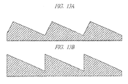
- a sectional shape of grooves of the reflection-type blazed diffraction grating suitable for the spectrophotometer is not a saw-tooth shape, as shown in FIG. 13B , but it is an asymmetric triangular waveform having a convex portion with an apex angle of about 90°.
- the angle p is 1/2 of an angle formed by an entrance slit center, a diffraction grating and an exit slit center in the spectrophotometer.
- a short side is required to be kept vertical to a surface of the diffraction grating regardless of an inclined angle of the long side, but in the diffraction grating shown in FIG. 13A , when the inclined angle of the long side is changed in response to a wavelength, diffraction efficiency of which should be maximized according to the Equation 1, it is also needed to change an inclined angle of the short side to the surface of the diffraction grating.
- the diffraction grating for a spectrophotometer is conventionally manufactured by a machine ruling system mainly using a ruling engine or a holographic exposure system based upon a two-beam interference using laser.
- the groove shape shown in FIG. 13A can be produced by the ruling engine using a diamond blade edge having an apex angle of about 90° in a tool.
- a technique of forming a periodic pattern on a photoresist film by holographic exposure, performing oblique ion beam etching using the photoresist film as a mask, thereby manufacturing a blazed diffraction grating is also disclosed.
- advance in technique is significant in a semiconductor manufacturing field, and as described in Patent Literature 2 or 3, a technique of manufacturing a blazed diffraction grating using the photolithography technique is disclosed.
- a forming technique of a diffraction grating using a ruling engine there are (1) a forming technique of a diffraction grating using a ruling engine and (2) a forming technique of a diffraction grating using the holographic exposure.
- Non-Patent Literature 1 Keiei KUDO, July, 1985, "BASE AND METHOD of SPECTRUM", Ohmsha Ltd .
- the diffraction efficiency of the blazed diffraction grating is determined according to the inclined angle and the flatness of a reflection surface, corresponding to the long side in the above-described sectional view and mainly contributing to diffracted light, of two reflection surfaces forming an asymmetric triangular-waveform section in FIG. 13A , and the squareness of the angle formed by the two faces.
- the disturbance of a groove period, roughness of the reflection surface corresponding to the long side, non-uniformity of a shape near an apex formed by intersection of two faces forming the saw-tooth waveform, and the like are known.
- holographic exposure system is advantageous for securing the flatness or the roughness of a face constituting grooves, or the like as compared with the ruling engine, but the holographic exposure system cannot satisfy the demand for forming grooves at optional unequal intervals.
- a sectional shape of grooves of a diffraction grating manufactured by the technique described in the above-described Patent Literature 2 or 3 is a saw-tooth shape such as that shown in FIG.
- Patent Literatures 2 and 3 describe a technique of making a rising angle of the short side vertical to the diffraction grating surface but they does not include a technique for making the short side orthogonal to the long side which is needed to be changed variously, and it is impossible to ensure the asymmetric triangular-waveform sectional shape as that shown in FIG. 13A .
- the present invention has been made in view of the foregoing, and an obj ect thereof is to provide a manufacturing technique capable of manufacturing a diffraction grating suitable for use in a spectrophotometer and capable of satisfying a high diffraction efficiency and a low stray light amount in a state where an apex angle of a convex portion is about 90°.
- the present invention has been made in view of the problems in (1) the forming technique of a diffraction grating utilizing the ruling engine and (2) the forming technique of a diffraction grating utilizing the holographic exposure, and a representative preferred aim thereof is to provide a manufacturing technique of a diffraction grating capable of achieving accuracy improvement of a product and reduction of a manufacturing time of the product.
- a representative preferred aim thereof is to provide a manufacturing technique of a diffraction grating capable of achieving accuracy improvement of a product and reduction of a manufacturing time of the product.
- a manufacturing method solving the above problem is as follows:
- a summary of a typical invention is that method of manufacturing a diffraction grating having a blazed sectional shape, including: shaping light emitted from a light source to an illumination shape being asymmetric with respect to an optical axis and causing the light to pass through a mask provided with predetermined periodic patterns; causing zero-order light and first-order light generated by causing the light to pass through the mask to interfere with each other on a surface of the substrate and expose a photosensitive material on the surface of the substrate; and forming a diffraction grating having the blazed sectional shape on the substrate.
- the method when exposing a photosensitive material on a surface of the substrate, includes: causing light emitted from the light source to pass through the mask via the aperture, causing zero-order light and first-order light generated by causing the light to pass through the mask to interfere with each other on a surface of the substrate to expose the photosensitive material on a defocus side of a focal range where a constant imaging performance can be maintained, and forming a diffraction grating having the blazed sectional shape on the substrate.
- a diffraction grating with a convex portion having an apex angle of about 90° capable of satisfying a high diffraction efficiency and a low stray light amount can be manufactured.
- a diffraction grating with a convex portion having an apex angle of about 90° can be manufactured without performing etching to a pattern formed by exposure.
- a typical effect can provide a manufacturing technique of a diffraction grating capable of achieving accuracy improvement of a product and reduction of a manufacturing time.
- the diffraction grating 100 shown in FIG. 2 is a reflection-type blazed diffraction grating with a groove period of 1.6 ⁇ m suitable for use in a spectrophotometer, which is configured such that when a monochromator of Czerny-Turner type mount where ⁇ in Equation 1 is 12° is used, the highest diffraction efficiency is obtained at a wavelength of 546 nm.
- the inclined angle of the long side becomes about 10.05° and the depth of the groove becomes about 0.275 ⁇ m.
- each of these numerical values is only one example, and the effect of the present invention is not limited to these numerical values or a combination(s) thereof.
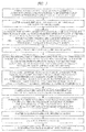
- FIG. 3 shows a procedure of manufacturing the diffraction grating 100 on a Si wafer.
- the term "gray-scale mask” indicates a photo mask configured so as to be capable of substantially changing the transmittance for each place on the photo mask such that exposure can be performed while the exposure amount is changed in a plural step fashion for each place within a shot region on a substrate of a Si wafer or the like simultaneously exposed by a reduction projection exposure apparatus.
- a diffraction grating with a convex portion having an apex angle of about 90° capable of achieving high diffraction efficiency and a low stray light amount can be manufactured.
- a diffraction grating with a convex portion having an apex angle of about 90° can be manufactured.
- Step 1 to Step 6 shown in FIG. 3 shows a result obtained by actually manufacturing a gray-scale mask and using a Si wafer to perform exposure test, but instead, the optimal exposure condition of an exposure apparatus can also be determined by a computer simulation.
- a computer simulation means (hereinafter, called “exposure simulator”) can obtain, as numerical data, a solid geometry of a three-dimensional photoresist pattern which will be formed as the result obtained by performing the procedure from Step 1 to Step 4 in FIG. 3 according to computer simulation by inputting the transmittance distribution data of the gray-scale mask, the exposure characteristic of the reduction projection exposure apparatus, characteristics such as the sensitivity of the photoresist, and actual numerical values of other required parameters into the computer simulation means, and the optimal exposure conditions can be determined using this exposure simulator.
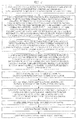
- FIG. 4 A diffraction grating manufacturing procedure when an exposure simulator is used is shown in FIG. 4 .
- Step of manufacturing an actual gray-scale mask (Step 5 shown in FIG. 4 ) has been inserted before Step 7 shown in FIG. 3 .
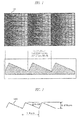
- FIG. 1 The structure of the gray-scale mask 10 used in the procedure shown in FIG. 3 or FIG. 4 is shown in FIG. 1 .
- the gray-scale mask 10 shown in FIG. 1 is a binary mask composed of one of an opening portion which allows exposure beam to pass through at an substantially-constant high transmittance and a light-shielding portion which almost blocks exposure beam and does not allow the exposure beam to pass through for each location, where lengths of a long side and a short side of a small opening represented by one rectangle in FIG. 1 are set equal to or less than a resolution limit of a reduction projection exposure apparatus used in the procedure. Therefore, in a light amount distribution of the light projected onto the Si wafer through the reduction projection exposure apparatus, small openings in FIG. 1 are not resolved at all, and the gray-scale mask 10 functions as a gray-scale mask whose transmittance virtually continuously changes in proportion to an aperture ratio of the small opening at the location for each location.
- the small openings having the same width are arranged in a direction orthogonal to a longitudinal direction of a groove of the diffraction grating 100, but if the aperture ratio distributions for respective locations are set equal to one another, the small openings having the same width may be arranged in a direction parallel to the longitudinal direction of the groove of the diffraction grating 100, as shown in FIG. 7 . Further, if the aperture ratio distributions for respective locations are set equal to one another, the shape of the small openings may be changed to the rectangles having different widths to circles having different diameters, or such an arrangement that a distribution density of circles having a constant diameter varies may be adopted.
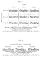
- FIG. 5 Examples of a sectional shape of a three-dimensional photoresist pattern formed when exposure is performed by using the gray-scale mask 10 shown in FIG. 1 and changing the exposure amount and the focus value at Step 2 in FIG. 3 are shown in FIG. 5 . It is understood that a sectional shape obtained when a combination of the focus value of -0.4 ⁇ m and the exposure amount of 180 mJ/cm 2 is adopted is proximate to the sectional shape shown in FIG. 2 .
- FIG. 6 examples of a sectional shape of a three-dimensional photoresist pattern formed when, in addition to setting the focus value and the exposure amount to the above-described combination, the numerical aperture (NA) of the exposure lens is fixed to 0.6, and exposure is performed while the sigma ( ⁇ ) value of illumination is changed are shown in FIG. 6 . It is understood that the sectional shape obtained when the ⁇ value is 0. 6 is approximate to the sectional shape shown in FIG. 2 . In this case, the ⁇ value of illumination is determined as 0.6.
- Step 6 in FIG. 3 or Step 4 in FIG. 4 when it is necessary to further modify the sectional shape of the gray-scale mask 10, a difference between the sectional shape of the formed three-dimensional photoresist pattern and the sectional shape of a diffraction grating to be manufactured may be added to sectional shape data of Step 1 in FIG. 3 or FIG. 4 as a correction term.
- the correction term is a spatial frequency component at a higher order than the cyclic period of the grooves in the diffraction grating.
- a term obtained by multiplying the Sine waveform which is a harmonic of the cyclic period of the grooves in the diffraction grating by a proper coefficient may be added as the correction term in correction of the sectional shape of the gray-scale mask 10.
- the transmittance distribution corresponding to the arrangement of the grooves may be set at unequal intervals on the gray-scale mask 10.
- an ultraviolet part for example, a wavelength such as 365nm, 248nm, 193nm or the like is used, but another wavelength may be used.
- the photoresist is directly applied to the Si wafer, but when a standing wave in the photoresist film results in adverse effect, an antireflection film may be applied on the Si wafer before application of the photoresist.
- the Al film is directly formed on the three-dimensional photoresist pattern having been formed, but a dielectric film may be formed on the three-dimensional photoresist pattern as a protective coating before formation of the Al film.
- the member obtained by forming the Al film on the three-dimensional photoresist pattern formed on the Si wafer is used as the diffraction grating as it is, but a member obtained by etching the Si wafer using the three-dimensional photoresist pattern as an etching mask and transferring the sectional shape of the three-dimensional photoresist pattern to the Si wafer itself may be used as the diffraction grating; or another substrate, such as, for example, a glass substrate which has been applied with resin for pattern transfer, to which a surface shape of the three-dimensional photoresist pattern is transferred by pressing (crimping) or the like may be used as the diffraction grating.
- photoresist such a low-gamma photoresist that a difference in photoresist-remaining film between an exposed portion and an unexposed portion is substantially proportional to the exposure amount of the exposed portion may be used.
- FIG. 9 shows a procedure for manufacturing a diffraction grating 100 on a Si wafer.
- the diffraction grating manufacturing procedure is as that shown in FIG. 10 .
- the structure of the binary mask 20 used in the procedure shown in FIG. 9 or FIG. 10 is shown in FIG. 8 .
- the binary mask shown in FIG. 8 is composed of periodic repetition of straight slit-shaped opening portions allowing pass of exposure beam with an substantially high transmittance and shielding portions existing between the opening portions and almost blocking exposure beam to prevent passing through thereof.
- the cyclic period corresponds to a groove period P of a diffraction grating to be manufactured.
- N the smoother the flatness of the reflection face of a three-dimensional photoresist pattern to be formed becomes, as described later; but the number of repetitions of exposure increases and a time required for exposure increases correspondingly, so that the magnitude (the value) of N should be determined based upon the tradeoff between the flatness and the time.
- the optimal overlap amount is determined.
- FIG. 12 shows the configuration of a spectrophotometer equipped with the diffraction grating 100 manufactured by the method of manufacturing a diffraction grating shown in the aspect of the example 1 or the aspect of the example 2.
- White light emitted from a light source 201 is incident on a monochromator 202.
- the monochromator 202 houses the diffraction grating 100 driven by a wavelength driving system 209 therein, and a monochromic light with a desired measurement wavelength is taken out according to a command from a CPU 207.
- the sample side beam 203 passes through a sample 205 to be affected by spectral absorption characteristic of the sample.
- the concentration of the sample is high, the sample side beam is strongly subjected to absorption, so that the simple side beam 203 after passing through the sample 205 develops weak intensity.
- a measurement value includes an error corresponding to the intensity of the stray light.
- the sample side beam 203 and the reference side beam 204 are incident on light detectors 206, respectively.
- Output signals of the light detectors 206 are taken in the CPU 207, where the absorbance of the sample 205 at the desired wavelength is computed from an intensity ratio of both the output signals and the absorbance is converted to the concentration of the sample 205.
- a diffraction grating having a high diffraction efficiency and reduced stray light can be manufactured, when a spectrophotometer equipped with the diffraction grating is configured, a light amount of weak light to be measured can be measured with an excellent S/N ratio and a concentration value of the sample can be measured accurately with excellent linearity even regarding a sample having a high concentration and a large light absorption amount.
- the number of the elements when referring to the number of elements (including number of pieces, values, amount, range, and the like), the number of the elements is not limited to a specific number unless otherwise stated or except the case where the number is apparently limited to a specific number in principle. The number larger or smaller than the specified number is also applicable.
- the components are not always indispensable unless otherwise stated or except the case where the components are apparently indispensable in principle.
- the shape of the components, positional relation thereof, and the like are mentioned, the substantially approximate and similar shapes and the like are included therein unless otherwise stated or except the case where it is conceivable that they are apparently excluded in principle. The same goes for the numerical value and the range described above.
- a method of manufacturing a diffraction grating which is an embodiment of the present invention is applied to a manufacturing method of a diffraction grating having a blazed sectional shape, a feature thereof is that light emitted from a light source (an illumination light source 10) is shaped to an illumination shape asymmetric with respect to an optical axis (using an aperture 20), it is caused to pass through a mask with a predetermined periodic pattern (mask 40), zero-order light and first-order light generated by causing the light to pass through the mask are caused to interfere with each other on a surface of a substrate (Si wafer 60) to expose a photosensitive material (photoresist 70) on the surface of the substrate so that a diffraction grating having a blazed sectional shape on the substrate is formed (as one example, components corresponding to FIG. 14 are quoted in parentheses).
- a first embodiment of the present invention will be described with reference to FIG. 14A to FIG. 20D .
- a diffraction grating of the first embodiment when an illumination shape asymmetric with respect to an optical axis is formed, an aperture having an opening portion being asymmetric with respect to the optical axis is used. Further, as the mask, a mask on which patterns are disposed corresponding to blazed pitches (equal intervals, unequal intervals) of a diffraction grating is used.
- FIGS. 14A to 14E are schematic diagrams showing one example of the exposure apparatus.
- FIG. 14A represents a schematic configuration of the exposure apparatus
- FIG. 14B represents a shape of an aperture
- FIG. 14C represents a shape of a mask
- FIG. 14D represents details around DOF for exposing a photoresist on a Si wafer
- FIG. 14E represents optical images and resist shapes at positions of + defocus and - defocus.
- the exposure apparatus is composed of an illumination light source 10, an aperture 20, a condensing lens 30, a mask 40, a projection lens 50, and the like.
- the exposure apparatus is an apparatus which utilizes a three-dimensional resist pattern forming technique using a deformed illumination method to expose a photoresist 70 applied to a surface of a Si wafer 60.
- the illumination light source 10 is a light source for performing exposure.
- the aperture 20 is provided with an opening portion 21 being asymmetric with respect to an optical axis of the illumination light source 10, and it is for shaping light emitted from the illumination light source 10 to an illumination shape asymmetric with respect to the optical axis.
- the opening portion 21 is a portion allowing passing of light and the other portion thereof is a light-shielding portion 22 blocking light.
- a circular opening portion 21 (white representation) is provided on the right side of the optical axis (intersection between X axis and Y axis).
- the condensing lens 30 is a lens for condensing light which has passed through the opening portion 21 of the aperture 20 on the mask 40.
- the mask 40 is provided with predetermined periodic patterns, and the patterns are disposed corresponding to blazed pitches of the mask 40.
- the patterns of the mask 40 are composed of repetition of lines 41 which are light-shielding portions for blocking light and spaces 42 which are transmissive portions allowing transmission of light.
- lines 41 black line representation
- spaces 42 white line representation
- the projection lens 50 is a lens for projecting the repetitive pattern of the lines 41 and the spaces 42 on the mask 40 on a photoresist 70 of the Si wafer 60.
- a reduction projection exposure apparatus which reduces a pattern of the mask 40 to project the same will be described.
- a deformed illumination method is used.
- the deformed illumination method is an illumination method that inserts an aperture provided with an opening portion 21 which is not positioned on an optical axis of an optical system to cause exposure beam to obliquely enter the mask 40.
- the resolution and the DOF depth of focus
- the DOF means a focal range where constant focusing perfarmance can be maintained.
- the photoresist 70 on the Si wafer 60 is exposed at a defocus position on the - (negative) side (a side near the illumination light source 10) (- defocus) and a defocus potion on the + (positive) side (a side far from the illumination light source 10) (+ defocus) relative to a just focus position of the DOF.
- This embodiment has a feature such that, when the photoresist 70 on the surface of the Si wafer 60 is exposed by the exposure apparatus using the described-above deformed illumination method, light emitted from the illumination light source 10 is caused to pass through the mask 40 via the aperture 20, and the zero-order light and the first-order light generated by causing the light to pass through the mask 40 are caused to interfere with each other on the surface of the Si wafer 60 to expose the photoresist 70 at the + defocus position or the - defocus position of the DOF, so that a diffraction grating which has been formed with the photoresist 70 having the blazed sectional shape on the Si wafer 60 is formed.
- FIG. 15 is a schematic diagram showing one example of an aperture used in the exposure apparatus.
- FIG. 16A to FIG. 16C are schematic diagrams showing one example of a mask and a resist shape used in the exposure apparatus.
- FIG. 16A shows a summary of the mask
- FIG. 16B shows a sectional shape of a photoresist corresponding to the mask shown in FIG. 16A
- FIG. 16C shows a sectional shape of a photoresist corresponding to the mask shown in FIG. 16A according to simulation.
- the example of the sectional shapes of the photoresist shown in FIG. 16B and 16C corresponds to the case where exposure has been performed at the + defocus position. Incidentally, in the case where exposure has been performed at the - defocus position, the shapes are inverted.
- FIGS. 17A to 17E the modified examples of the aperture shown in FIG. 15 will be described.
- FIG. 17A to 17E show sectional shapes of photoresists which have been obtained by simulation together with shapes of apertures, respectively. Further, for easy understanding of differences from the shapes of the modified examples, the example of the circular opening portion shown in FIG. 15 is illustrated in FIG. 17A .
- diffraction gratings can be formed similarly by adopting apertures providing with an opening portion asymmetric with respect to an optical axis, such as shown in FIGS. 17B to 17E.
- FIG. 17B shows an example of an aperture 20a provided with a semi-circular opening portion 21a (white representation)
- FIG. 17C shows an example of an aperture 20b provided with two circular opening portions 21b (white representation)
- FIG. 17D shows an example of an aperture 20c provided with a semi-ring-shaped opening portion 21c (white representation)
- FIG. 17E shows an example of an aperture 20d provided with a 1/6 ring-shaped opening portion 21d (white representation).
- a diffraction grating in which an equally-spaced blazed photoresist 70 has been formed on the Si wafer 60 and the Al film has been formed on the photoresist 70 can be manufactured.
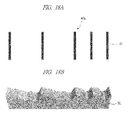
- FIGS. 18A and 18B are schematic diagrams showing a mask and a first modified example having a resist shape.
- FIG. 18A shows a summary of the mask
- FIG. 18B shows a sectional shape of a photoresist corresponding to the mask shown FIG. 18A obtained by simulation.
- a diffraction grating can be similarly formed to a mask 40a having an unequally-spaced layout pattern, such as that shown in FIG. 18A .
- five lines 41 black line representation
- a diffraction grating where a unequally-spaced blazed photoresist 70 has been formed on a Si wafer 60 and an Al film has been formed on the photoresist 70 can be manufactured.
- such an unequally-spaced diffraction grating for example, it can be used in (1) a situation that aberration of a concave diffraction grating is reduced and resolution is improved, (2) a situation that an imaging surface of a concave diffraction grating is a curved face, but the imaging face is made flat so that a diode array detector or a CCD (Charge Coupled Device) can be used, (3) a situation that an imaging performance is brought to a flat diffraction grating, and the like.
- CCD Charge Coupled Device
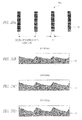
- FIGS. 19A and 19E are schematic diagrams showing a mask and a second modified example having a resist shape.
- FIG. 19A shows a summary of a mask having auxiliary patterns (Y direction)
- FIG. 19B shows a summary of a mask having auxiliary patterns (X direction)
- FIG. 19C shows a sectional shape of a photoresist corresponding to a mask having no auxiliary patterns according to simulation
- FIG. 19D shows a sectional shape of a photoresist corresponding to the mask of FIG. 19A having auxiliary patterns (Y direction) according to simulation
- FIG. 19E shows a sectional shape of a photoresist corresponding to the mask of FIG. 19B having auxiliary patterns (X direction).
- the aperture 20 (20a to 20d) provided with an opening portion asymmetric with respect to an optical axis, such as that described above, is used, and a mask 40b having lines 43a (black line representation) of an auxiliary pattern arranged in the Y direction in addition to the lines 41a (black line representation) of the main pattern, as shown in FIG. 19A , or a mask 40c having lines 43b (black line representation) of the auxiliary pattern arranged in the X direction in addition to lines 41b (black line representation) of the main pattern, as shown in FIG. 19B , is used.
- angles (depths) of the blazed diffraction grating by adjusting the size of the auxiliary pattern (a line width of a line, the number of lines, or the like).
- the angle of the blazed diffraction grating is also called "blazed angle", and it is shown as ⁇ in FIG. 19C . Further, the depth of the blazed diffraction grating is shown as d in FIG. 19C .
- the blazed angle can be made smaller than that in the sectional shape of the photoresist 70 shown in FIG. 19C corresponding to the mask having no auxiliary pattern (corresponding to the mask 40 shown in FIG. 16A ). In other words, the depth can be made shallow.
- the blazed angle can be made small (the depth can be made shallow) .
- Such a diffraction grating whose angles (depths) can be changed can be used, in a case that angles in one diffraction grating (the same pitch) are equal, a case that angles in one diffraction grating are different, or the like. Further, even when angles in one diffraction grating (the same pitch) are equal, there are such a diffraction grating in which each angle is large (the depth is deep), such as that shown in FIG. 19C , a diffraction grating in which each angle is small (the depth is shallow), such as that shown in FIGS. 19D and 19E , and the like.
- angles in one diffraction grating are different is used, for example, in a case that a diffraction grating is divided into four pieces such that each angle in a first piece are small (the depth is shallow), each angle in a second piece is large (the depth is deep), each angle in a third piece is small, and each angle in a fourth piece is large, and the diffraction efficiency is increased in a wide wavelength range.
- FIGS. 20A to 20D are schematic diagrams showing the third modified example of a mask and a resist shape.
- FIG. 20A shows summary of a line-and-space mask arranged to have a resolution equal to or less than a resolution limit
- FIG. 20B shows a sectional shape of a photoresist corresponding to a mask in which a length of the lines and spaces in FIG. 20A is 100 nm according to simulation
- FIG. 20C shows a sectional shape of a photoresist corresponding to a mask in which a length of the lines and spaces in FIG. 20A is 150 nm according to simulation
- FIG. 20D shows a sectional shape of a photoresist corresponding to a mask in which a length of the lines and spaces in FIG. 20A is 200 nm according to simulation.
- a mask 40d where fine lines and spaces 44 (a line portion is represented by a black line) having pitches equal to or less than the resolution limit, shown in FIG. 20A are arranged at a pitch of a desired diffraction grating is used.
- the blazed angle can be made large (the depth can be made deeper) according to changes of the length X of the lines and spaces 44 to 100 nm ⁇ 150 nm ⁇ 200 nm.
- Such a diffraction grating where the angles (the depths) can be changed is used in an application similar to that of a diffraction grating such as that shown in FIGS. 19A to 19E .
- the following advantageous effects can be obtained by using the aperture 20 (20a to 20d) provided with an opening portion 21 (21a to 21d) being asymmetric with respect to an optical axis and using the mask 40 (40a to 40d) in which patterns are arranged corresponding to blazed pitches in the diffraction grating, causing light emitted from the illumination light source 10 to pass through the mask 40 (40a to 40d) via the aperture 20 (20a to 20d), causing zero-order light and first-order light, which are generated by causing the light to pass through the mask 40 (40a to 40d), to interfere with each other on the surface of the Si wafer 60 to expose the photoresist 70 on the surface of the Si wafer 60 on the + defocus side or the - defocus side of the DOF, and manufacturing a diffraction grating in which the photoresist 70 having the equally-spaced or unequally-spaced blazed sectional shape with equal angles (depths) or different angles (depths)
- FIGS. 21A to 21C A second embodiment of the present invention will be described with reference to FIGS. 21A to 21C .
- a first aperture provided with an opening portion being asymmetric with respect to the optical axis and a second aperture provided with an opening portion being asymmetric with respect to the first aperture and inverted therefrom are used.
- a mask in which patterns are arranged corresponding to brazed pitches (equal intervals, unequal intervals) of a diffraction grating is used.
- FIGS. 21A to 21C are schematic diagrams showing one example of an aperture and a resist shape used in the exposure apparatus
- FIG. 21A shows a sectional shape of a photoresist according to simulation when the DOF has been applied to only the deformed illumination method on the right side using the first aperture
- FIG. 21B shows a sectional shape of a photoresist according to simulation when the DOF has been applied to only the deformed illumination method on the left side using the second aperture
- FIG. 21C shows a sectional shape of a photoresist according to simulation when a double exposure DOF of the deformed illumination method has been applied using the first aperture and the second aperture.
- the aperture 20 shown in FIG. 21A is the same as the aperture shown in FIG. 15 , and it has a circular opening portion 21 (white representation) allowing transmission of light provided on the right side of the optical axis.
- the result of simulation using the aperture 20 has shown that the sectional shape of the photoresist is x (bad) at the - defocus position of -1.5 ⁇ m, it is ⁇ (slightly good) at the - defocus position of -1.3 ⁇ m, it is O (good) at the - defocus positions of -1.1 ⁇ m, -0.9 ⁇ m, and 0.7 ⁇ m, it is ⁇ at the - defocus position of -0.5 ⁇ m, and it is x at the - defocus positions of -0.3 ⁇ m and -0.1 ⁇ m.
- an aperture 80 shown in FIG. 21B is provided with an opening portion 21 inverted regarding the aperture 20 shown in FIG. 21A , where a circular opening portion 21 allowing transmission of light (white representation) is provided on the left side of the optical axis.
- the result of simulation using the aperture 80 has shown that the sectional shape of a photoresist is x at the - defocus position of -0.1 ⁇ m, it is ⁇ at the + defocus position of +0.1 ⁇ m, it is O at the + defocus positions of +1.3 ⁇ m, +0.5 ⁇ m, and +0.7 ⁇ m, it is ⁇ at the + defocus position of +0.9 ⁇ m, and it is x at the + defocus positions of +1.1 ⁇ m and +1.3 ⁇ m.
- the aperture 20 shown in FIG. 21A and the aperture 80 shown in FIG. 21B are used, the first exposure is performed using the aperture 20 shown in FIG. 21A , and the second exposure is performed using the aperture 80 shown in FIG. 21B .
- the result of simulation using the two apertures 20 and 80 has shown that the sectional shapes of the photoresist is O at the respective defocus positions of a combination of -1.5 ⁇ m and -0.1 ⁇ m, a combination of -1.3 ⁇ m and +0.1 ⁇ m, a combination of -1.1 ⁇ m and +0.3 ⁇ m, a combination of -0.9 ⁇ m and +0.5 ⁇ m, a combination of -0.7 ⁇ m and +0.7 ⁇ m, a combination of -0. 5 ⁇ m and +0. 9 ⁇ m, a combination of -0.3 ⁇ m and +1.1 ⁇ m, and a combination of -0.1 ⁇ m and +1.3 ⁇ m.
- a diffraction grating with improved focus margin can be formed.
- the method of manufacturing a diffraction grating (double exposure) will be described.
- the aperture can be modified in the same manner as the first embodiment, where if there are each of the apertures 20a to 20d shown in FIGS. 17B to 17E and an aperture whose shape has been mirror-inverted regarding each of the apertures 20a to 20d, as apertures other than the apertures 20 and 80 shown in FIGS. 21A and 21B , a diffraction grating can be formed similarly.
- the mask can be modified in the same manner as the first embodiment, where regarding not only the equally-spaced mask 40 shown in FIG. 16A but also the unequally-spaced mask 40a shown in FIG. 18A , the angle (depth) -changeable masks 40b and 40c, shown in FIGS. 19A and 19B , where the auxiliary patterns have been arranged in addition to the main patterns, and the angle (depth) -changeable mask 40d, shown in FIG. 20A , where the lines and spaces has been arranged to have a resolution equal to or less than a resolution limit, a diffraction grating can be similarly formed.
- advantageous effects similar to those of the first embodiment can be obtained by using the aperture 20 (20a to 20d) provided with an opening portion asymmetric with respect to an optical axis and the aperture 80 provided with an inverted opening portion asymmetric with respect to the aperture 20 and using the mask 40 (40a to 40d) where patterns are arranged corresponding to blazed pitches in the diffraction grating, causing light emitted from the illumination light source to pass through the mask 40 (40a to 40d) via the aperture 20 (20a to 20d) and the aperture 80, causing zero-order light and first-order light generated by causing the light to pass through the mask 40 (40a to 40d) to interfere with each other on the surface of the Si wafer to expose the photoresist on the + defocus side and/or the - defocus side of the DOF, and manufacturing a diffraction grating where the photoresist having the equally-spaced or unequally-space blazed sectional shape with equal angles (depths) or different angles
- FIGS. 22A and 22B and FIGS. 23A and 23B A third embodiment of the present invention will be described with reference to FIGS. 22A and 22B and FIGS. 23A and 23B .
- a diffraction grating when an illumination shape asymmetric with respect to an optical axis is formed, an aperture provided with an opening portion being symmetric with respect to an optical axis is used in an inclined fashion with respect to the optical axis.
- a mask in which patterns are arranged corresponding to blazed pitches (equally spaced, or unequally spaced) of a diffraction grating is used.
- FIGS. 22A and 22B are schematic diagrams showing one example of an exposure apparatus and an aperture used therein
- FIG. 22A shows summary of a tilted illumination method used in the exposure apparatus
- FIG. 22B shows a shape of an aperture
- FIGS. 23A and 23B are schematic diagrams showing one example of a mask used in the exposure apparatus shown in FIG. 22A and a resist shape
- FIG. 23A shows a summary of the mask
- FIG. 23B shows a sectional shape of a photoresist corresponding to the mask shown in FIG. 23A according to simulation.
- the third embodiment is configured to obtain an effect similar to a deformed illumination in a pseudo manner by tilting an aperture 90 as shown in FIG. 22A without making the illumination shape asymmetric like the first and second embodiments. That is, as the aperture 90, one provided with an opening portion 23 symmetrical with respect to an optical axis, as shown by a broken line in FIG. 22B is used. When a photoresist on a surface of a Si wafer is exposed, the aperture 90 is tilted to X axis passing through the optical axis by a tilt angle (for example, 20°). Thereby, an illumination shape provided with an opening portion 24 (white representation) asymmetric with respect to the optical axis in a pseudo manner can be formed, as shown in FIG. 22B .
- a tilt angle for example, 20°
- a diffraction grating with a photoresist 70 having a blazed sectional shape can be formed.
- the aperture can be modified in the same manner as the first embodiment such that, when an aperture with an opening portion symmetrical with respect to the optical axis obtained by changing each of the apertures 20a to 20d shown in FIGS. 17B to 17E is used as an aperture other than the aperture 90 shown in FIGS. 22A and 22B , a diffraction grating can be formed by performing exposure in an tilted state similarly.
- a diffraction grating can be formed by performing exposure in an tilted state similarly.
- an aperture with a circular opening portion can be obtained by modifying the opening portion shown in FIG. 17B
- an aperture with four circular opening portions can be obtained by modifying the opening portions shown in FIG. 17C
- an aperture with a ring-shaped opening portion can be obtained by modifying the opening portion shown in FIG. 17D
- an aperture with two 1/6 ring-shaped opening portion can be obtained by modifying the opening portion shown in FIG. 17E .
- the mask can be modified in the same manner as the first embodiment, where regarding not only the equally-spaced mask 40 shown in FIG. 23A but also the unequally-spaced mask 40a shown in FIG. 18A , the angle (depth) -changeable masks 40b and 40c, shown in FIGS. 19A and 19B , where the auxiliary patterns have been arranged in addition to the main patterns, and the angle (depth) -changeable mask 40d, shown in FIG. 20A , where the lines and spaces has been arranged to have a resolution less than or equal to a resolution limit, a diffraction grating can be similarly formed.
- advantageous effects similar to those of the first embodiment can be obtained by using the aperture 90 provided with an opening portion symmetrical with respect to an optical axis in a titling fashion to the optical axis and using the mask 40 (40a to 40d) where patterns are arranged corresponding to blazed pitches in the diffraction grating, causing light emitted from the illumination light source to pass through the mask 40 (40a to 40d) via the aperture 90, causing zero-order light and first-order light generated by causing the light to pass through the mask 40 (40a to 40d) to interfere with each other on the surface of the Si wafer to expose the photoresist on the + defocus side or the - defocus side of the DOF, and manufacturing a diffraction grating where the photoresist having the equally-spaced or unequally-spaced blazed sectional shape with equally-angled (depth) or unequally-angled (depth) has been formed on the Si wafer.
- the illumination shape asymmetric with respect to an optical axis is achieved by using an aperture, but the present invention is not limited to such a method, and such an apparatus that an illumination light source itself emits light having an illumination shape asymmetric with respect to an optical axis can be used.
- the aperture to be used is not limited to each of the apertures provided with the opening portions having the shapes shown in FIGS. 17A to 17E , and the shape of the opening portion may be modified variously.
- blazed angle (depth) is changed regarding the mask, a mask having auxiliary patterns different from auxiliary patterns such as shown in FIGS. 19A or 19B or a mask having lines and spaces different from lines and spaces such as those shown in FIG. 20A can be used.
- the present invention is not limited to the method of manufacturing a diffraction grating, and it can be applied to a semiconductor device manufacturing method including an asymmetric shape.
- an asymmetric shape can be formed on a semiconductor substrate by applying one of the first to third embodiments to a portion of MEMS (Micro Electro Mechanical Systems).
- MEMS Micro Electro Mechanical Systems
- the asymmetric sectional shape is not limited to the photosensitive material and a sectional shape of a photosensitive material is transferred to a semiconductor substrate by applying a known semiconductor etching process, so that an asymmetric sectional shape can be formed on the semiconductor substrate.
- the method of manufacturing a diffraction grating of the present invention can be particularly applied to a method for manufacturing a diffraction grating having a blazed sectional shape by applying a three-dimensional resist pattern forming technique using a deformed illumination method.
Landscapes
- Physics & Mathematics (AREA)
- General Physics & Mathematics (AREA)
- Spectroscopy & Molecular Physics (AREA)
- Optics & Photonics (AREA)
- Engineering & Computer Science (AREA)
- Manufacturing & Machinery (AREA)
- Diffracting Gratings Or Hologram Optical Elements (AREA)
- Spectrometry And Color Measurement (AREA)
- Health & Medical Sciences (AREA)
- High Energy & Nuclear Physics (AREA)
- Toxicology (AREA)
Abstract
Description
- The present invention relates to a diffraction grating manufacturing method for dispersing incident light to respective wavelengths. In particular, the present invention relates to a manufacturing method of a reflection-type one-dimensional blazed diffraction grating suitable for use in a spectrophotometer, which can take out diffracted light with a particular order of diffraction efficiently.
- The present invention relates to a diffraction grating manufacturing method, and in particular to a technique suitably applied to a manufacturing method of a brazed diffraction grating having a blazed-shaped (saw-tooth wave-shaped) sectional configuration. The present invention relates to a technique suitably applied to a semiconductor device manufacturing method including an asymmetric shape.
- As described on pages 435 to 442 in
Non-Patent Literature 1, a wavelength-dispersive spectrophotometer measures the transmittance or the reflectance of the sample by dispersing light emitted from a light source and taking out only a light component having a desired wavelength to irradiate a sample with the light component or by taking out only a light component having a desired wavelength after guiding light emitted from a light source to a sample. In the wavelength-dispersive spectrophotometer, diffraction gratings with grooves arranged periodically in one-dimensional direction are widely used. - In the spectrophotometer, since it is required to utilize energy of the light source effectively to perform measurement at a high S/N ratio, a reflection-type blazed diffraction grating which can take out only diffracted light with a particular order of diffraction efficiently is preferred in use as the kind of the diffraction grating.
- Further, since the spectrophotometer is generally frequently used over a wide wavelength range, it is desired to obtain significant diffraction efficiency in a wide incident angle range. Therefore, a sectional shape of grooves of the reflection-type blazed diffraction grating suitable for the spectrophotometer is not a saw-tooth shape, as shown in
FIG. 13B , but it is an asymmetric triangular waveform having a convex portion with an apex angle of about 90°. - In the blazed diffraction grating, an inclined long side mainly contributes to reflection of diffracted light, but when incident light is vertically incident on the long side, the diffraction efficiency reaches the maximum, and a relationship of

- In a diffraction grating shown in
FIG. 13B , a short side is required to be kept vertical to a surface of the diffraction grating regardless of an inclined angle of the long side, but in the diffraction grating shown inFIG. 13A , when the inclined angle of the long side is changed in response to a wavelength, diffraction efficiency of which should be maximized according to theEquation 1, it is also needed to change an inclined angle of the short side to the surface of the diffraction grating. - As described on pages 364 to 382 in
Non-Patent Literature 1, the diffraction grating for a spectrophotometer is conventionally manufactured by a machine ruling system mainly using a ruling engine or a holographic exposure system based upon a two-beam interference using laser. - The groove shape shown in
FIG. 13A can be produced by the ruling engine using a diamond blade edge having an apex angle of about 90° in a tool. On the other hand, in the holographic exposure system, only a diffraction grating having a groove having a sectional shape of Sin waveform (sine waveform, sinusoidal waveform) or a shape close to that could be manufactured. In recent years, however, for example, as described inPatent Literature 1, a technique of forming a periodic pattern on a photoresist film by holographic exposure, performing oblique ion beam etching using the photoresist film as a mask, thereby manufacturing a blazed diffraction grating is also disclosed. Further, recently, advance in technique is significant in a semiconductor manufacturing field, and as described inPatent Literature - As the method of manufacturing a diffraction grating, for example, there are (1) a forming technique of a diffraction grating using a ruling engine and (2) a forming technique of a diffraction grating using the holographic exposure.
- (1) The forming technique of a diffraction grating using a ruling engine is a technique of forming a blazed diffraction grating by machining utilizing the ruling engine using a diamond tool.
- (2) The forming technique of a diffraction grating using the holographic exposure is a technique of forming a blazed diffraction grating by performing oblique etching to a resist pattern which has been subj ected to holographic exposure. For example, as a technique regarding the holographic exposure, there are techniques described in Japanese Patent Application Laid-Open Publication No.
2005-11478 2006-259325 -
- Patent Literature 1: Japanese Patent Application Laid-Open Publication No.
H11-305023 - Patent Literature 2: Japanese Patent Application Laid-Open Publication No.
2007-155927 - Patent Literature 3: Japanese Patent Application Laid-Open Publication No.
2002-189112 - Patent Literature 4: Japanese Patent Application Laid-Open Publication No.
2005-11478 - Patent Literature 5: Japanese Patent Application Laid-Open Publication No.
2006-259325 - Non-Patent Literature 1: Keiei KUDO, July, 1985, "BASE AND METHOD of SPECTRUM", Ohmsha Ltd.
- When the transmittance or the reflectance of a sample in a desired wavelength is measured by the wavelength-dispersive spectrophotometer, an efficiency of taking out a light component having the desired wavelength depends on the diffraction efficiency of the diffraction grating. On the other hand, mixing of a light component having a wavelength other than the desired wavelength into the light component having the desired wavelength during the measurement must be avoided since it causes error in measurement of the transmittance or the reflectance. Such a light component is called "stray light".
- In the diffraction grating used in the spectrophotometer, it is needless to say that it is required to ensure high diffraction efficiency and a low stray light amount. It is known that the diffraction efficiency of the blazed diffraction grating is determined according to the inclined angle and the flatness of a reflection surface, corresponding to the long side in the above-described sectional view and mainly contributing to diffracted light, of two reflection surfaces forming an asymmetric triangular-waveform section in
FIG. 13A , and the squareness of the angle formed by the two faces. As the causes of the stray light, the disturbance of a groove period, roughness of the reflection surface corresponding to the long side, non-uniformity of a shape near an apex formed by intersection of two faces forming the saw-tooth waveform, and the like are known. - From these facts, in manufacture of a blazed diffraction grating, it is required to ensure the inclined angle, the squareness of the angle formed by two faces, the groove periods, and the uniformity of a shape near an apex formed by intersection of two faces with a high degree of accuracy to realize an excellent flatness and a low roughness on the reflection surface. In the manufacturing method using the conventional ruling engine, however, since the accuracy of a face to be machined is determined depending on a shape accuracy or a face accuracy of a tool to be used (generally, a tool having a diamond blade edge is used) itself, it is difficult to improve the accuracy up to a certain level or more.
- As another request, there is such a request that periods of grooves should be set at unequal intervals for reduction of aberration generated at a spectroscopy time, a light condensing action or an imaging action simultaneously with a spectroscopy action, or the like. The holographic exposure system is advantageous for securing the flatness or the roughness of a face constituting grooves, or the like as compared with the ruling engine, but the holographic exposure system cannot satisfy the demand for forming grooves at optional unequal intervals.
- As compared with these techniques, it can be easily anticipated that the technique of utilizing a recent semiconductor manufacturing technique which has been advanced as described above is advantageous for both forming grooves at optionally unequal intervals and improving face accuracy of a main reflection face. However, a sectional shape of grooves of a diffraction grating manufactured by the technique described in the above-described
Patent Literature FIG. 13B , and thePatent Literatures FIG. 13A . - The present invention has been made in view of the foregoing, and an obj ect thereof is to provide a manufacturing technique capable of manufacturing a diffraction grating suitable for use in a spectrophotometer and capable of satisfying a high diffraction efficiency and a low stray light amount in a state where an apex angle of a convex portion is about 90°.
- Now, regarding a forming technique of a diffraction grating such as described above, as the present inventor's result of study, the following matters have been clarified.
- (1) Since the forming technique of a diffraction grating utilizing the ruling engine is machining, it has a limitation in accuracy improvement. Further, the forming technique is a dedicated technique for a diffraction grating and thus lacks expansivity. That is, the forming technique can only form parallel lines. In addition, the forming technique takes time for manufacturing a diffraction grating.
- (2) Since the forming technique (including the above-described
Patent Literatures 4 and 5) of a diffraction grating utilizing the holographic exposure requires an additional step, factors of variation in manufacture increase. That is, the diffraction grating only forms a sine curve, so that further exposure or machining is required in order to obtain an excellent diffraction grating. Further, a manufacturing apparatus for the additional step is required. Moreover, it is difficult to form non-periodic structure, unequal intervals or the like. - Therefore, the present invention has been made in view of the problems in (1) the forming technique of a diffraction grating utilizing the ruling engine and (2) the forming technique of a diffraction grating utilizing the holographic exposure, and a representative preferred aim thereof is to provide a manufacturing technique of a diffraction grating capable of achieving accuracy improvement of a product and reduction of a manufacturing time of the product.
025 The above and other preferred aims and novel characteristics of the present invention will be apparent from the description of the present specification and the accompanying drawings. - A manufacturing method solving the above problem is as follows:
- A method of manufacturing a diffraction grating, including: setting an exposure condition such that, with respect to an opening portion shape of a mask having an opening portion with a periodic structure, a sectional shape of a convex portion of a resist on a substrate, the convex having been formed by exposure, is an asymmetric triangle and an angle formed by a long side and a short side of the triangle is about 90°; and performing exposure.
- The typical ones of the inventions disclosed in the present application will be briefly described as follows.
- That is, a summary of a typical invention is that method of manufacturing a diffraction grating having a blazed sectional shape, including: shaping light emitted from a light source to an illumination shape being asymmetric with respect to an optical axis and causing the light to pass through a mask provided with predetermined periodic patterns; causing zero-order light and first-order light generated by causing the light to pass through the mask to interfere with each other on a surface of the substrate and expose a photosensitive material on the surface of the substrate; and forming a diffraction grating having the blazed sectional shape on the substrate.
- More preferably, when exposing a photosensitive material on a surface of the substrate, the method includes: causing light emitted from the light source to pass through the mask via the aperture, causing zero-order light and first-order light generated by causing the light to pass through the mask to interfere with each other on a surface of the substrate to expose the photosensitive material on a defocus side of a focal range where a constant imaging performance can be maintained, and forming a diffraction grating having the blazed sectional shape on the substrate.
- According to the present invention, a diffraction grating with a convex portion having an apex angle of about 90° capable of satisfying a high diffraction efficiency and a low stray light amount can be manufactured. In particular, a diffraction grating with a convex portion having an apex angle of about 90° can be manufactured without performing etching to a pattern formed by exposure.
- That is, a typical effect can provide a manufacturing technique of a diffraction grating capable of achieving accuracy improvement of a product and reduction of a manufacturing time.
-
-
FIG. 1 is a diagram showing a structure of a gray-scale mask used in a method of manufacturing a diffraction grating according to a first example of the present invention [First Technique]; -
FIG. 2 is a diagram showing a section of a diffraction grating manufactured by the method of manufacturing a diffraction grating according to the first example of the present invention [First Technique]; -
FIG. 3 is a diagram showing a procedure of the method of manufacturing a diffraction grating according to the first example of the present invention [First Technique]; -
FIG. 4 is a diagram showing another procedure of the method of manufacturing a diffraction grating according to the first example of the present invention [First Technique]; -
FIG. 5 is a diagram showing an effect obtained when a focus value and an exposure amount are changed in the method of manufacturing a diffraction grating according to the first example of the present invention [First Technique]; -
FIG. 6 is a diagram showing an effect obtained when σ value of illumination is changed in the method of manufacturing a diffraction grating according to the first example of the present invention [First Technique]; -
FIG. 7 is a diagram showing another structure of the gray-scale mask used in the method of manufacturing a diffraction grating according to the first example of the present invention [First Technique]; -
FIG. 8 is a diagram showing a structure of a binary mask used in a method of manufacturing a diffraction grating according to a second example of the present invention [First Technique]; -
FIG. 9 is a diagram showing a procedure of the method of manufacturing a diffraction grating according to the second example of the present invention [First Technique]; -
FIG. 10 is a diagram showing another procedure of the method of manufacturing a diffraction grating according to the second example of the present invention [First Technique]; -
FIG. 11 is a diagram showing an effect obtained when an overlap amount is changed in the method of manufacturing a diffraction grating according to the second example of the present invention [First Technique]; -
FIG. 12 is a diagram showing a configuration of a spectrophotometer using a diffraction grating manufactured by a method of manufacturing a diffraction grating according to a third example of the present invention [First Technique]; -
FIGS. 13A and 13B are diagrams for explaining kinds of a sectional shape of a blazed diffraction grating [First Technique] ; -
FIGS. 14A to 14E are diagrams showing one example of an exposure apparatus realizing a method of manufacturing a diffraction grating of the first embodiment of the present invention [Second Technique] ; -
FIG. 15 is a schematic diagram showing one example of an aperture used in the exposure apparatus shown inFIGS. 14A to 14E [Second Technique]; -
FIGS. 16A to 16C are schematic diagrams showing one example of a mask and a resist shape used in the exposure apparatus shown inFIGS. 14A to 14E [Second Technique]; -
FIGS. 17A to 17E are schematic diagrams showing a modified example of the aperture shown inFIG. 15 and the resist shape [Second Technique]; -
FIGS. 18A and 18B are schematic diagrams showing a first modified example of the mask and the resist shape shown inFIGS. 16A to 16C [Second Technique]; -
FIGS. 19A to 19E are schematic diagrams showing a second modified example of the mask and the resist shape shown inFIGS. 16A to 16C [Second Technique]; -
FIGS. 20A to 20D are schematic diagrams showing a third modified example of the mask and the resist shape shown inFIGS. 16A to 16C [Second Technique]; -
FIGS. 21A to 21C are schematic diagrams showing one example of apertures and resist shapes used in the exposure apparatus shown inFIGS. 14A to 14E of a second embodiment of the present invention [Second Technique] ; -
FIGS. 22A and 22B are schematic diagrams showing one example of an exposure apparatus for achieving a method of manufacturing a diffraction grating of a third embodiment of the present invention and an aperture used in the exposure apparatus [Second Technique] ; and -
FIGS. 23A and 23B are schematic diagrams showing one example of a mask and a resist shape used in the exposure apparatus shown inFIGS. 22A and 22B . - Hereinafter, embodiment of the present invention will be described with reference to the drawings.
- Here, as an example of a sectional shape of a diffraction grating to be manufactured, explanation will be made with reference to a
diffraction grating 100 shown inFIG. 2 . - The
diffraction grating 100 shown inFIG. 2 is a reflection-type blazed diffraction grating with a groove period of 1.6 µm suitable for use in a spectrophotometer, which is configured such that when a monochromator of Czerny-Turner type mount where σ inEquation 1 is 12° is used, the highest diffraction efficiency is obtained at a wavelength of 546 nm. Here, the inclined angle of the long side becomes about 10.05° and the depth of the groove becomes about 0.275 µm. - Incidentally, each of these numerical values is only one example, and the effect of the present invention is not limited to these numerical values or a combination(s) thereof.
-
FIG. 3 shows a procedure of manufacturing thediffraction grating 100 on a Si wafer. Here, the term "gray-scale mask" indicates a photo mask configured so as to be capable of substantially changing the transmittance for each place on the photo mask such that exposure can be performed while the exposure amount is changed in a plural step fashion for each place within a shot region on a substrate of a Si wafer or the like simultaneously exposed by a reduction projection exposure apparatus. - Step 1: A gray-
scale mask 10 having a transmission distribution substantially proportional to a depth distribution of a groove in a section of a diffraction grating to be manufactured is manufactured. - Step 2: After a photoresist is applied to a Si wafer for test exposure by a spin coater, the Si wafer is pre-baked.
- Step 3 : The transmittance distribution on the gray-
scale mask 10 is transferred to the Si wafer obtained atStep 2 by using the gray-scale mask 10 in a reduction projection exposure apparatus. Here, while a region is changed on the Si wafer, the transfer is repeated by a plurality of shots by changing each of the focus value, the exposure amount, the numerical aperture of an exposure lens, and the σ value of illumination (the σ value is a ratio of the numerical aperture of a light source to the numerical aperture of the projection lens) of the exposure apparatus in a plural step fashion. - Step 4: After the Si wafer at
Step 3 is developed, it is post-baked. - Step 5: A sectional shape of a three-dimensional photoresist pattern formed on the Si wafer of
Step 4 is measured. A shot where the sectional shape optimally coincides with a sectional shape (for example,FIG. 3 in this example) of a diffraction grating to be manufactured is selected and the focus value and the exposure amount thereof are recorded as an optimal exposure condition. - Step 6: If excellent match with a sectional shape of a diffraction grating to be manufactured cannot be found in any of the shots, the transmittance distribution of the gray-
scale mask 10 manufactured atStep 1 is changed, a new gray-scale mask is manufactured, and the procedure fromStep 2 toStep 5 is repeated again. When any shot where a sectional shape excellently matching with the sectional shape of a diffraction grating to be manufactured exists, the control proceeds to a procedure atStep 7. - Step 7: After a photoresist is applied on a Si wafer for diffraction grating manufacture by a spin coater, the Si wafer is pre-baked.
- Step 8: The transmittance distribution on the
gray mask 10 is transferred to the Si wafer obtained atStep 7 using the gray-scale mask 10 in a reduction projection exposure apparatus. At this time, the focus value and the exposure amount recorded atStep 5 are set in the exposure apparatus. - Step 9: After the Si wafer obtained at
Step 8 is developed, it is post-baked. - Step 10: An Al film is formed on the Si wafer obtained at
Step 9. - Step 11: A diffraction grating formed at
Step 10 is diced to a proper size. - According to the above-described Steps, a diffraction grating with a convex portion having an apex angle of about 90° capable of achieving high diffraction efficiency and a low stray light amount can be manufactured. In particular, even if etching is not performed to a pattern which has been formed by exposure, a diffraction grating with a convex portion having an apex angle of about 90° can be manufactured.
- The procedure from
Step 1 to Step 6 shown inFIG. 3 shows a result obtained by actually manufacturing a gray-scale mask and using a Si wafer to perform exposure test, but instead, the optimal exposure condition of an exposure apparatus can also be determined by a computer simulation. - A computer simulation means (hereinafter, called "exposure simulator") can obtain, as numerical data, a solid geometry of a three-dimensional photoresist pattern which will be formed as the result obtained by performing the procedure from
Step 1 toStep 4 inFIG. 3 according to computer simulation by inputting the transmittance distribution data of the gray-scale mask, the exposure characteristic of the reduction projection exposure apparatus, characteristics such as the sensitivity of the photoresist, and actual numerical values of other required parameters into the computer simulation means, and the optimal exposure conditions can be determined using this exposure simulator. - A diffraction grating manufacturing procedure when an exposure simulator is used is shown in
FIG. 4 . In this procedure, Step of manufacturing an actual gray-scale mask (Step 5 shown inFIG. 4 ) has been inserted beforeStep 7 shown inFIG. 3 . - The structure of the gray-
scale mask 10 used in the procedure shown inFIG. 3 orFIG. 4 is shown inFIG. 1 . - The gray-
scale mask 10 shown inFIG. 1 is a binary mask composed of one of an opening portion which allows exposure beam to pass through at an substantially-constant high transmittance and a light-shielding portion which almost blocks exposure beam and does not allow the exposure beam to pass through for each location, where lengths of a long side and a short side of a small opening represented by one rectangle inFIG. 1 are set equal to or less than a resolution limit of a reduction projection exposure apparatus used in the procedure. Therefore, in a light amount distribution of the light projected onto the Si wafer through the reduction projection exposure apparatus, small openings inFIG. 1 are not resolved at all, and the gray-scale mask 10 functions as a gray-scale mask whose transmittance virtually continuously changes in proportion to an aperture ratio of the small opening at the location for each location. - In
FIG. 1 , the small openings having the same width are arranged in a direction orthogonal to a longitudinal direction of a groove of thediffraction grating 100, but if the aperture ratio distributions for respective locations are set equal to one another, the small openings having the same width may be arranged in a direction parallel to the longitudinal direction of the groove of thediffraction grating 100, as shown inFIG. 7 . Further, if the aperture ratio distributions for respective locations are set equal to one another, the shape of the small openings may be changed to the rectangles having different widths to circles having different diameters, or such an arrangement that a distribution density of circles having a constant diameter varies may be adopted. - Examples of a sectional shape of a three-dimensional photoresist pattern formed when exposure is performed by using the gray-
scale mask 10 shown inFIG. 1 and changing the exposure amount and the focus value atStep 2 inFIG. 3 are shown inFIG. 5 . It is understood that a sectional shape obtained when a combination of the focus value of -0.4 µm and the exposure amount of 180 mJ/cm2 is adopted is proximate to the sectional shape shown inFIG. 2 . - Next, examples of a sectional shape of a three-dimensional photoresist pattern formed when, in addition to setting the focus value and the exposure amount to the above-described combination, the numerical aperture (NA) of the exposure lens is fixed to 0.6, and exposure is performed while the sigma (σ) value of illumination is changed are shown in
FIG. 6 . It is understood that the sectional shape obtained when the σ value is 0. 6 is approximate to the sectional shape shown inFIG. 2 . In this case, the σ value of illumination is determined as 0.6. - Also, at
Step 6 inFIG. 3 orStep 4 inFIG. 4 , when it is necessary to further modify the sectional shape of the gray-scale mask 10, a difference between the sectional shape of the formed three-dimensional photoresist pattern and the sectional shape of a diffraction grating to be manufactured may be added to sectional shape data ofStep 1 inFIG. 3 orFIG. 4 as a correction term. - As a cause for occurrence of the difference between the sectional shape of the formed three-dimensional photoresist pattern and the sectional shape of a diffraction grating to be manufactured, there is generally lack in resolution of the reduction projection exposure apparatus or lack in number of gradations of change of the aperture ratio distribution in the gray-
scale mask 10, so that the correction term is a spatial frequency component at a higher order than the cyclic period of the grooves in the diffraction grating. Therefore, instead of addition of the difference between the sectional shape of the formed three-dimensional photoresist pattern and the sectional shape of a diffraction grating to be manufactured as the correction term, a term obtained by multiplying the Sine waveform which is a harmonic of the cyclic period of the grooves in the diffraction grating by a proper coefficient may be added as the correction term in correction of the sectional shape of the gray-scale mask 10. - In the gray-
scale mask 10 inFIG. 1 , the case where intervals of grooves in the diffraction grating are constant is described, but since the periods of the grooves should be made unequal for reducing the aberration generated when the diffraction grating is used in the spectrophotometer, so as to cause the gray-scale mask to have a light condensing action or an imaging action simultaneously with a spectroscopy action, or the like, the transmittance distribution corresponding to the arrangement of the grooves may be set at unequal intervals on the gray-scale mask 10. - In this embodiment as configured as described above, since such a configuration as to control at least one of the focus, the exposure amount, the numerical aperture of the exposing lens, the σ value of illumination, and the transmittance distribution on the gray-scale mask of the reduction projection exposure apparatus is adopted in order to perform reduction projection exposure using the gray-scale mask and to cause the sectional shape of the three-dimensional photoresist pattern formed at the time of the reduction projection exposure to coincide with the sectional shape of a diffraction grating to be manufactured, a blazed diffraction grating which is suitably used in a spectrophotometer and has a sectional shape with a high precision where an apex angle of a convex portion is about 90° can be manufactured.
- In this example, as the exposure wavelength of the reduction projection exposure apparatus, an ultraviolet part, for example, a wavelength such as 365nm, 248nm, 193nm or the like is used, but another wavelength may be used.
- In this example, the photoresist is directly applied to the Si wafer, but when a standing wave in the photoresist film results in adverse effect, an antireflection film may be applied on the Si wafer before application of the photoresist.
- In this embodiment, the Al film is directly formed on the three-dimensional photoresist pattern having been formed, but a dielectric film may be formed on the three-dimensional photoresist pattern as a protective coating before formation of the Al film.
- In this example, the member obtained by forming the Al film on the three-dimensional photoresist pattern formed on the Si wafer is used as the diffraction grating as it is, but a member obtained by etching the Si wafer using the three-dimensional photoresist pattern as an etching mask and transferring the sectional shape of the three-dimensional photoresist pattern to the Si wafer itself may be used as the diffraction grating; or another substrate, such as, for example, a glass substrate which has been applied with resin for pattern transfer, to which a surface shape of the three-dimensional photoresist pattern is transferred by pressing (crimping) or the like may be used as the diffraction grating.
- Further, as the photoresist, such a low-gamma photoresist that a difference in photoresist-remaining film between an exposed portion and an unexposed portion is substantially proportional to the exposure amount of the exposed portion may be used.
- These modified example may be applied to Example 2.
- A second example of the present invention will be described with reference to each of
FIG. 8 to FIG. 11 . -
FIG. 9 shows a procedure for manufacturing adiffraction grating 100 on a Si wafer. - Step 1: A
binary mask 20 in which a plurality of straight slit-shaped openings, which have a width equal to substantially one-Nth of the groove period obtained by dividing the groove period of a diffraction grating to be manufactured, are arranged in a plurality of rows in parallel corresponding to the groove periods is manufactured. - Step 2: After a photoresist is applied to a Si wafer for test exposure by a spin coater, the Si wafer is pre-baked.
- Step 3: While the
binary mask 20 is discretely shifted to the Si wafer ofStep 2 in the arrangement direction of the grooves in the diffraction grating in a reduction projection exposure apparatus, exposure is performed while the exposure amount is changed for each shift. At this time, while a region is changed on the Si wafer, the transfer is repeated by a plurality of shots by changing each of the focus value, the exposure amount, the numerical aperture of an exposure lens, and the σ value of illumination of the exposure apparatus in a plural-step fashion. - Step 4: After the Si wafer of
Step 3 is developed, it is post-baked. - Step 5: A sectional shape of a three-dimensional photoresist pattern formed on the Si wafer of
Step 4 is measured. A shot in which the sectional shape is the best match with a sectional shape (for example,FIG. 13A ) of a diffraction grating to be manufactured is selected, and the focus value and the exposure level for each shift are recorded as optimal exposure conditions. - Step 6: If excellent match with a sectional shape of a diffraction grating to be manufactured cannot be found in any of the shots, the opening width of the
binary mask 20 manufactured atStep 1 is changed, a new binary mask is manufactured, and the procedure fromStep 2 toStep 5 is repeated again. When any shot where a sectional shape excellently matches with the sectional shape of a diffraction grating to be manufactured exists, the control proceeds to a procedure atStep 7. - Step 7: After a photoresist is applied on a Si wafer for diffraction grating manufacture by a spin coater, the Si wafer is pre-baked.
- Step 8: While the
binary mask 20 is discretely shifted to the Si wafer ofStep 7 in the arrangement direction of the grooves in the diffraction grating in the reduction projection exposure apparatus, exposure is performed with an exposure amount determined for each shift. At this time, the focus value and the exposure level for each shift which have been recorded atStep 5 are set in the exposure apparatus. - Step 9: After the Si wafer of
Step 8 is developed, it is post-baked. - Step 10: An Al film is formed on the Si wafer of
Step 9. - Step 11: A diffraction grating formed at
Step 10 is diced to a proper size. - Regarding the procedure from
Step 1 toStep 6 inFIG. 9 , when the optimal exposure condition is determined using the exposure simulator like the first example, the diffraction grating manufacturing procedure is as that shown inFIG. 10 . - The structure of the
binary mask 20 used in the procedure shown inFIG. 9 orFIG. 10 is shown inFIG. 8 . The binary mask shown inFIG. 8 is composed of periodic repetition of straight slit-shaped opening portions allowing pass of exposure beam with an substantially high transmittance and shielding portions existing between the opening portions and almost blocking exposure beam to prevent passing through thereof. The cyclic period corresponds to a groove period P of a diffraction grating to be manufactured. - The width W of the opening in a short side direction (however, showing a size of the opening projected on the Si wafer) is set to a width equal to each width of about N pieces obtained by division of the groove period of the diffraction grating to be manufactured (W > P/N), where a numerical value of N = about 4 to 8 is adopted as N. The larger N, the smoother the flatness of the reflection face of a three-dimensional photoresist pattern to be formed becomes, as described later; but the number of repetitions of exposure increases and a time required for exposure increases correspondingly, so that the magnitude (the value) of N should be determined based upon the tradeoff between the flatness and the time.
- While the binary mask having the opening portions having the width W is shifted by a pitch S in a direction orthogonal to the groove direction of the diffraction grating to be manufactured, exposure is performed N times. Setting is performed such that S < W and a relationship of S x N = P are satisfied. At this time, in exposure in each stage, overlap with the previous exposure region by W - S occurs, but even if S is constant, an overlap amount can be changed by changing W. When the overlap amount is changed, the sectional shape of a three-dimensional photoresist pattern formed by exposure is changed like
FIG. 11 , for example. In the example shown inFIG. 11 , it is understood that the sectional shape becomes proximate to the sectional shape shown inFIG. 2 in the case of the overlap amount = 200 nm. Thus, the optimal overlap amount is determined. In addition, the course of changing the focus, the exposure amount, the numerical aperture of the exposure lens, and the σ value of illumination of the reduction projection exposure apparatus such that the sectional shape of the three-dimensional photoresist pattern to be formed becomes proximate to the sectional shape of the diffraction grating to be manufactured, and the configuration required therefor are similar to those in the first Example. - A third example of the present invention will be described with reference to
FIG. 12. FIG. 12 shows the configuration of a spectrophotometer equipped with thediffraction grating 100 manufactured by the method of manufacturing a diffraction grating shown in the aspect of the example 1 or the aspect of the example 2. - White light emitted from a
light source 201 is incident on amonochromator 202. Themonochromator 202 houses thediffraction grating 100 driven by awavelength driving system 209 therein, and a monochromic light with a desired measurement wavelength is taken out according to a command from aCPU 207. After the monochromic light is divided into asample side beam 203 and areference side beam 204, thesample side beam 203 passes through asample 205 to be affected by spectral absorption characteristic of the sample. Here, when the concentration of the sample is high, the sample side beam is strongly subjected to absorption, so that thesimple side beam 203 after passing through thesample 205 develops weak intensity. At this time, if the diffraction efficiency of thediffraction grating 100 is low, the light amount of thelight source 201 cannot be utilized sufficiently, so that a high S/N cannot be obtained. Further, when a component other than a desired wavelength, which is not absorbed by thesample 205, so-called "stray light" is included in the sample beam, a measurement value includes an error corresponding to the intensity of the stray light. - After passing through the
sample 205, thesample side beam 203 and thereference side beam 204 are incident on light detectors 206, respectively. Output signals of the light detectors 206 are taken in theCPU 207, where the absorbance of thesample 205 at the desired wavelength is computed from an intensity ratio of both the output signals and the absorbance is converted to the concentration of thesample 205. According to the method of manufacturing a diffraction grating shown in the first example or the second example of the present invention, since a diffraction grating having a high diffraction efficiency and reduced stray light can be manufactured, when a spectrophotometer equipped with the diffraction grating is configured, a light amount of weak light to be measured can be measured with an excellent S/N ratio and a concentration value of the sample can be measured accurately with excellent linearity even regarding a sample having a high concentration and a large light absorption amount. - The following embodiment will be described being divided into a plurality of embodiments or sections for convenience sake if necessary, but unless expressly stated otherwise, these embodiments or sections are not independent from one another, where one thereof is in a relationship with a modified example, details, a supplementary explanation, or the like of a portion or entirety of the other. However, these sections or embodiments are not irrelevant to each other unless otherwise stated, and the one relates to the entire or a part of the other as a modification example, details, or a supplementary explanation thereof. Also, in the embodiments described below, when referring to the number of elements (including number of pieces, values, amount, range, and the like), the number of the elements is not limited to a specific number unless otherwise stated or except the case where the number is apparently limited to a specific number in principle. The number larger or smaller than the specified number is also applicable.
- Further, in the embodiments described below, it goes without saying that the components (including element steps) are not always indispensable unless otherwise stated or except the case where the components are apparently indispensable in principle. Similarly, in the embodiments described below, when the shape of the components, positional relation thereof, and the like are mentioned, the substantially approximate and similar shapes and the like are included therein unless otherwise stated or except the case where it is conceivable that they are apparently excluded in principle. The same goes for the numerical value and the range described above.
- Hereinafter, embodiments of the present invention will be described in detail with reference to the accompanying drawings. Note that components having the same function are denoted by the same reference symbols throughout the drawings for describing the embodiment, and the repetitive description thereof will be omitted.
- A method of manufacturing a diffraction grating which is an embodiment of the present invention is applied to a manufacturing method of a diffraction grating having a blazed sectional shape, a feature thereof is that light emitted from a light source (an illumination light source 10) is shaped to an illumination shape asymmetric with respect to an optical axis (using an aperture 20), it is caused to pass through a mask with a predetermined periodic pattern (mask 40), zero-order light and first-order light generated by causing the light to pass through the mask are caused to interfere with each other on a surface of a substrate (Si wafer 60) to expose a photosensitive material (photoresist 70) on the surface of the substrate so that a diffraction grating having a blazed sectional shape on the substrate is formed (as one example, components corresponding to
FIG. 14 are quoted in parentheses). - Respective embodiments based upon the summary of the embodiment of the present invention which has been described above are specifically described below. The embodiments described below are examples using the present invention and the present invention is not limited by the following embodiments.
- A first embodiment of the present invention will be described with reference to
FIG. 14A to FIG. 20D . - In a method of manufacturing a diffraction grating of the first embodiment, when an illumination shape asymmetric with respect to an optical axis is formed, an aperture having an opening portion being asymmetric with respect to the optical axis is used. Further, as the mask, a mask on which patterns are disposed corresponding to blazed pitches (equal intervals, unequal intervals) of a diffraction grating is used. When a photoresist on a surface of a Si wafer is exposed, light emitted from a light source is caused to pass through the mask via the aperture, zero-order light and first-order light generated by causing the light to pass through the mask are caused to interfere with each other on a surface of the Si wafer, and a photoresist is exposed on a defocus side (+ defocus side, - defocus side) of a focal range where a constant imaging performance can be maintained, a diffraction grating having a blazed sectional shape is formed on the Si wafer. In the following, the first embodiment will be described specifically with reference to
FIG. 14A to FIG. 20D . - Referring to
FIGS. 14A to 14E , an exposure apparatus realizing a method of manufacturing a diffraction grating according to the first embodiment will be described.FIGS. 14A to 14E are schematic diagrams showing one example of the exposure apparatus.FIG. 14A represents a schematic configuration of the exposure apparatus,FIG. 14B represents a shape of an aperture,FIG. 14C represents a shape of a mask,FIG. 14D represents details around DOF for exposing a photoresist on a Si wafer, andFIG. 14E represents optical images and resist shapes at positions of + defocus and - defocus. - As shown in
FIG. 14A , the exposure apparatus according to the first embodiment is composed of anillumination light source 10, anaperture 20, a condensinglens 30, amask 40, aprojection lens 50, and the like. The exposure apparatus is an apparatus which utilizes a three-dimensional resist pattern forming technique using a deformed illumination method to expose aphotoresist 70 applied to a surface of aSi wafer 60. - The
illumination light source 10 is a light source for performing exposure. As theillumination light source 10, for example, g-line or i-line, an excimer laser of KrF, ArF, or the like, is used. - As shown in
FIG. 14B (details are illustrated inFIG. 15 ), theaperture 20 is provided with an openingportion 21 being asymmetric with respect to an optical axis of theillumination light source 10, and it is for shaping light emitted from theillumination light source 10 to an illumination shape asymmetric with respect to the optical axis. In theaperture 20, the openingportion 21 is a portion allowing passing of light and the other portion thereof is a light-shieldingportion 22 blocking light. In the example of theaperture 20 shown inFIG. 14B , a circular opening portion 21 (white representation) is provided on the right side of the optical axis (intersection between X axis and Y axis). - The condensing
lens 30 is a lens for condensing light which has passed through the openingportion 21 of theaperture 20 on themask 40. - As shown in
FIG. 14C (details are illustrated inFIG. 16A ), themask 40 is provided with predetermined periodic patterns, and the patterns are disposed corresponding to blazed pitches of themask 40. The patterns of themask 40 are composed of repetition oflines 41 which are light-shielding portions for blocking light andspaces 42 which are transmissive portions allowing transmission of light. In the example shown inFIG. 14C , four lines 41 (black line representation) arranged at equal intervals are provided and spaces 42 (white line representation) are disposed amongrespective lines 41. - The
projection lens 50 is a lens for projecting the repetitive pattern of thelines 41 and thespaces 42 on themask 40 on aphotoresist 70 of theSi wafer 60. Incidentally, in a method of manufacturing a diffraction grating described later, a reduction projection exposure apparatus which reduces a pattern of themask 40 to project the same will be described. - In the exposure apparatus configured as described above, a deformed illumination method is used. The deformed illumination method is an illumination method that inserts an aperture provided with an opening
portion 21 which is not positioned on an optical axis of an optical system to cause exposure beam to obliquely enter themask 40. According to the deformed illumination method, the resolution and the DOF (depth of focus) can be improved by performing exposure using only zero-order light and first-order light diffracted by themask 40. The DOF means a focal range where constant focusing perfarmance can be maintained. - In this embodiment, as shown in
FIG. 14D , thephotoresist 70 on theSi wafer 60 is exposed at a defocus position on the - (negative) side (a side near the illumination light source 10) (- defocus) and a defocus potion on the + (positive) side (a side far from the illumination light source 10) (+ defocus) relative to a just focus position of the DOF. - As a result of simulation of exposure of the
photoresist 70 on theSi wafer 60 which has been performed at the + defocus position and the - defocus position, optical images (light intensity distributions) and resist shapes such as those shown inFIG. 14E have been obtained. That is, it has been found that the resist shapes can be formed to have a blazed sectional shapes and the shapes at the + defocus position and the - defocus position are inversed to each other. That is, at the - defocus position, such saw teeth are obtained that they have a steep inclination from each top of the saw teeth toward a V-shaped groove on the left side and a gentle inclination from each top of the saw teeth toward a V-shaped groove on the right side. On the other hand, at the + defocus position, such saw teeth are obtained that they have a gentle inclination from each top of the saw teeth toward a V-shaped groove on the left side and a steep inclination therefrom toward a V-shaped groove on the right side. - This embodiment has a feature such that, when the
photoresist 70 on the surface of theSi wafer 60 is exposed by the exposure apparatus using the described-above deformed illumination method, light emitted from theillumination light source 10 is caused to pass through themask 40 via theaperture 20, and the zero-order light and the first-order light generated by causing the light to pass through themask 40 are caused to interfere with each other on the surface of theSi wafer 60 to expose thephotoresist 70 at the + defocus position or the - defocus position of the DOF, so that a diffraction grating which has been formed with thephotoresist 70 having the blazed sectional shape on theSi wafer 60 is formed. <Manufacturing Method of Diffraction Grating> - With reference to
FIG. 15 and FIGS. 16A to 16C , a method of manufacturing a diffraction grating using the exposure apparatus shown inFIG. 14A will be described.FIG. 15 is a schematic diagram showing one example of an aperture used in the exposure apparatus.FIG. 16A to FIG. 16C are schematic diagrams showing one example of a mask and a resist shape used in the exposure apparatus.FIG. 16A shows a summary of the mask,FIG. 16B shows a sectional shape of a photoresist corresponding to the mask shown inFIG. 16A, and FIG. 16C shows a sectional shape of a photoresist corresponding to the mask shown inFIG. 16A according to simulation. The example of the sectional shapes of the photoresist shown inFIG. 16B and 16C corresponds to the case where exposure has been performed at the + defocus position. Incidentally, in the case where exposure has been performed at the - defocus position, the shapes are inverted. - (1) An
aperture 20 provided with an openingportion 21 asymmetric with respect to an optical axis is prepared. In theaperture 20, the circular opening portion 21 (white representation) which allows passing through of light is provided on the right side of the optical axis, for example, as shown inFIG. 15 . - (2) A
mask 40 having line patterns arranged at pitches of a diffraction grating to be manufactured is prepared. In thismask 40, four lines 41 (black line representation) arranged at equal intervals and shielding light andspaces 42 provided among therespective lines 41 and allowing transmission of light are provided, for example, as shown inFIG. 16A . - (3) After a photoresist is applied to a Si wafer for test exposure by a spin coater, the Si wafer is pre-baked.
- (4) Patterns are transferred on the Si wafer at the above-described (3) using the
mask 40 in a reduction projection exposure apparatus. At this time, exposure is performed at the + defocus side or the - defocus side of the DOF, and while a region is changed on the Si wafer, the transfer is repeated by a plurality of shots by changing each of the focus value, the exposure amount, the numerical aperture of an exposure lens, of the exposure apparatus in a plural-step fashion. - (5) After the Si wafer at the above-described (4) is developed, it is post-baked if necessary.
- (6) A sectional shape of a three-dimensional photoresist pattern formed on the Si wafer of the above (5) is measured. A shot where the sectional shape optimally matches with a sectional shape (for example,
FIGS. 16B and 16C in this embodiment) of a diffraction grating to be manufactured is selected and the focus value and the exposure amount of the shot are recorded as optimal exposure conditions. - (7) If excellent match with a sectional shape of a diffraction grating to be manufactured cannot be found in any of the shots, the opening area, the opening position, and the opening shape of the
aperture 20 at the above-described (1) are changed, anew aperture 20 is used, and the procedure from the above-described (3) to (6) is repeated again. When any shot where a sectional shape excellently matches with the sectional shape of a diffraction grating to be manufactured exists, the control proceeds to a procedure performed at the following (8) in order to manufacture a diffraction grating of a product. - (8) After a
photoresist 70 is applied on aSi wafer 60 for diffraction grating manufacture by a spin coater, the Si wafer is pre-baked. - (9) The
mask 40 is transferred to theSi wafer 60 of the above-described (8) using theaperture 20 provided with an openingportion 21 asymmetric with respect to an optical axis in a reduction projection exposure apparatus. At this time, exposure is performed at the + defocus side or the - defocus side of the DOF, and the focus value and the exposure amount of the optimal exposure condition recorded at the above-described (6) are set in the exposure apparatus. - (10) After the
Si wafer 60 of the above-described (9) has been developed, it is subjected to post-baking, if necessary. At this time, a structure in which thephotoresist 70 having an equally-spaced blazed sectional shape has been formed on theSi wafer 60, for example, such as that shown inFIG. 16C , can be obtained. - (11) An Al film is formed on the
photoresist 70 on theSi wafer 60 of the above-described (10). - (12) A diffraction grating formed at the above-described (11) is diced to a proper size. Thereby, a product of a diffraction grating where an equally-spaced blazed
photoresist 70 has been formed on theSi wafer 60, and the Al film has been further formed on thephotoresists 70 is completed. - Referring to
FIGS. 17A to 17E , the modified examples of the aperture shown inFIG. 15 will be described.FIG. 17A to 17E show sectional shapes of photoresists which have been obtained by simulation together with shapes of apertures, respectively. Further, for easy understanding of differences from the shapes of the modified examples, the example of the circular opening portion shown inFIG. 15 is illustrated inFIG. 17A . - In addition to the
aperture 20 shown inFIG. 17A , diffraction gratings can be formed similarly by adopting apertures providing with an opening portion asymmetric with respect to an optical axis, such as shown inFIGS. 17B to 17E. FIG. 17B shows an example of anaperture 20a provided with asemi-circular opening portion 21a (white representation),FIG. 17C shows an example of anaperture 20b provided with two circular opening portions 21b (white representation),FIG. 17D shows an example of anaperture 20c provided with a semi-ring-shapedopening portion 21c (white representation), andFIG. 17E shows an example of anaperture 20d provided with a 1/6 ring-shapedopening portion 21d (white representation). Even in such modified examples, a diffraction grating in which an equally-spaced blazedphotoresist 70 has been formed on theSi wafer 60 and the Al film has been formed on thephotoresist 70 can be manufactured. - With reference to
FIGS. 18A and 18B , a first modified example of the mask shown inFIG. 16A will be described.FIGS. 18A and 18B are schematic diagrams showing a mask and a first modified example having a resist shape.FIG. 18A shows a summary of the mask, andFIG. 18B shows a sectional shape of a photoresist corresponding to the mask shownFIG. 18A obtained by simulation. - In addition to the
mask 40 having an equally-spaced layout pattern shown inFIG. 16A , a diffraction grating can be similarly formed to amask 40a having an unequally-spaced layout pattern, such as that shown inFIG. 18A . In the example of themask 40a shown inFIG. 18A , five lines 41 (black line representation) are provided at different pitches, respectively. In this modified example, as shown inFIG. 18B , a diffraction grating where a unequally-spaced blazedphotoresist 70 has been formed on aSi wafer 60 and an Al film has been formed on thephotoresist 70 can be manufactured. - As usages of such an unequally-spaced diffraction grating, for example, it can be used in (1) a situation that aberration of a concave diffraction grating is reduced and resolution is improved, (2) a situation that an imaging surface of a concave diffraction grating is a curved face, but the imaging face is made flat so that a diode array detector or a CCD (Charge Coupled Device) can be used, (3) a situation that an imaging performance is brought to a flat diffraction grating, and the like.
- With reference to
FIGS. 19A to 19E , a second modified example of the mask shown inFIG. 16A will be described.FIGS. 19A and 19E are schematic diagrams showing a mask and a second modified example having a resist shape.FIG. 19A shows a summary of a mask having auxiliary patterns (Y direction),FIG. 19B shows a summary of a mask having auxiliary patterns (X direction),FIG. 19C shows a sectional shape of a photoresist corresponding to a mask having no auxiliary patterns according to simulation,FIG. 19D shows a sectional shape of a photoresist corresponding to the mask ofFIG. 19A having auxiliary patterns (Y direction) according to simulation, andFIG. 19E shows a sectional shape of a photoresist corresponding to the mask ofFIG. 19B having auxiliary patterns (X direction). - The aperture 20 (20a to 20d) provided with an opening portion asymmetric with respect to an optical axis, such as that described above, is used, and a
mask 40b having lines 43a (black line representation) of an auxiliary pattern arranged in the Y direction in addition to thelines 41a (black line representation) of the main pattern, as shown inFIG. 19A , or amask 40c having lines 43b (black line representation) of the auxiliary pattern arranged in the X direction in addition tolines 41b (black line representation) of the main pattern, as shown inFIG. 19B , is used. In themask 40b and themask 40c, such as those described above, it is made possible to change angles (depths) of the blazed diffraction grating by adjusting the size of the auxiliary pattern (a line width of a line, the number of lines, or the like). The angle of the blazed diffraction grating is also called "blazed angle", and it is shown as θ inFIG. 19C . Further, the depth of the blazed diffraction grating is shown as d inFIG. 19C . - In the sectional shape of the
photoresist 70 shown inFIG. 19D corresponding to themask 40b with the auxiliary pattern (Y direction) shown inFIG. 19A , the blazed angle can be made smaller than that in the sectional shape of thephotoresist 70 shown inFIG. 19C corresponding to the mask having no auxiliary pattern (corresponding to themask 40 shown inFIG. 16A ). In other words, the depth can be made shallow. Similarly, even in the sectional shape of thephotoresist 70 shown inFIG. 19E corresponding to themask 40c with the auxiliary pattern (X direction) shown inFIG. 19B , the blazed angle can be made small (the depth can be made shallow) . - Such a diffraction grating whose angles (depths) can be changed can be used, in a case that angles in one diffraction grating (the same pitch) are equal, a case that angles in one diffraction grating are different, or the like. Further, even when angles in one diffraction grating (the same pitch) are equal, there are such a diffraction grating in which each angle is large (the depth is deep), such as that shown in
FIG. 19C , a diffraction grating in which each angle is small (the depth is shallow), such as that shown inFIGS. 19D and 19E , and the like. Further, the case that angles in one diffraction grating are different is used, for example, in a case that a diffraction grating is divided into four pieces such that each angle in a first piece are small (the depth is shallow), each angle in a second piece is large (the depth is deep), each angle in a third piece is small, and each angle in a fourth piece is large, and the diffraction efficiency is increased in a wide wavelength range. - A third modified example of the mask shown in
FIGS. 16A to 16C will be described with reference toFIGS. 20A to 20D. FIGS. 20A to 20D are schematic diagrams showing the third modified example of a mask and a resist shape.FIG. 20A shows summary of a line-and-space mask arranged to have a resolution equal to or less than a resolution limit,FIG. 20B shows a sectional shape of a photoresist corresponding to a mask in which a length of the lines and spaces inFIG. 20A is 100 nm according to simulation,FIG. 20C shows a sectional shape of a photoresist corresponding to a mask in which a length of the lines and spaces inFIG. 20A is 150 nm according to simulation, andFIG. 20D shows a sectional shape of a photoresist corresponding to a mask in which a length of the lines and spaces inFIG. 20A is 200 nm according to simulation. - The aperture 20 (20a to 20d) provided with an opening portion asymmetric with respect to an optical axis, such as that described above, is used, and a
mask 40d where fine lines and spaces 44 (a line portion is represented by a black line) having pitches equal to or less than the resolution limit, shown inFIG. 20A are arranged at a pitch of a desired diffraction grating is used. In themask 40d, it is made possible to change angles (depths) in the diffraction grating by changing the length X of the lines andspaces 44. - As shown in
FIGS. 20B, 20C and 20D , the blazed angle can be made large (the depth can be made deeper) according to changes of the length X of the lines andspaces 44 to 100 nm → 150 nm → 200 nm. Such a diffraction grating where the angles (the depths) can be changed is used in an application similar to that of a diffraction grating such as that shown inFIGS. 19A to 19E . - According to the first embodiment described above, the following advantageous effects can be obtained by using the aperture 20 (20a to 20d) provided with an opening portion 21 (21a to 21d) being asymmetric with respect to an optical axis and using the mask 40 (40a to 40d) in which patterns are arranged corresponding to blazed pitches in the diffraction grating, causing light emitted from the
illumination light source 10 to pass through the mask 40 (40a to 40d) via the aperture 20 (20a to 20d), causing zero-order light and first-order light, which are generated by causing the light to pass through the mask 40 (40a to 40d), to interfere with each other on the surface of theSi wafer 60 to expose thephotoresist 70 on the surface of theSi wafer 60 on the + defocus side or the - defocus side of the DOF, and manufacturing a diffraction grating in which thephotoresist 70 having the equally-spaced or unequally-spaced blazed sectional shape with equal angles (depths) or different angles (depths) has been formed on theSi wafer 60. - (1) As compared with the ruling engine, reduction in manufacturing time (for example, master manufacture: one month per one sheet → one day per one sheet) and accuracy improvement can be made possible, and formation of lines other than parallel lines can be made possible.
- (2) As compared with the holographic exposure, since an additional step such as an oblique etching is not required, reduction in manufacturing time and accuracy improvement of a product can be made possible. Further, a diffraction grating and another diffraction grating having unequal spaces or blazed angles/depths changed from that of the former diffraction grating can be formed simultaneously.
- (3) As an effect from the point of view of the entire product of the diffraction grating, the embodiment can contribute performance improvement of a diffraction grating such as diffraction efficiency improvement due to reduction in manufacturing variations or reduction in stray light.
- (4) As an effect from the point of view of the entire product of the diffraction grating, the embodiment can provide a manufacturing technique of a diffraction grating which can achieve accuracy improvement and reduction in manufacturing time of a product.
- The reasons why advantageous effects such as those of the above-described (1) to (4) are obtained are as follows:
- (11) Since the photolithography technique is a manufacturing method with a high throughput for responding to mass production of semiconductor products, it is possible to reduce a manufacturing time.
- (12) Since the photolithography technique is a technique of forming a pattern by utilizing a short-wavelength light source for responding to miniaturization and high precision of semiconductor products, it is possible to achieve high precision as compared with the ruling engine which performs ruling with a diamond tool having the same size as a diffraction grating to be manufactured.
- (13) Since this embodiment makes it possible to cause an optical image to have inclination by one-time exposure, an additional step is not required. Therefore, it is made possible to reduce manufacturing variations and improve machining precision as compared with the holographic exposure requiring an additional step.
- (14) Since the lithographic technique is a technique for transferring an arbitrary mask layout pattern on a photoresist applied to a Si wafer, unequally-spaced patterns can be formed. Further, since there is also an applied technology where a blazed angles can be changed by arranging auxiliary patterns, a diffraction grating and another diffraction grating having blazed angles/depths changed from that of the former diffraction grating can be formed simultaneously.
- A second embodiment of the present invention will be described with reference to
FIGS. 21A to 21C . - In a method of manufacturing a diffraction grating of the second embodiment, when an illumination shape being asymmetric with respect to an optical axis is formed, a first aperture provided with an opening portion being asymmetric with respect to the optical axis and a second aperture provided with an opening portion being asymmetric with respect to the first aperture and inverted therefrom are used. Further, as the mask, a mask in which patterns are arranged corresponding to brazed pitches (equal intervals, unequal intervals) of a diffraction grating is used. When a photoresist is exposed on a surface of a Si wafer, light emitted from a light source is caused to pass through the mask via the first aperture and the second aperture, zero-order light and first-order light generated by causing the light to pass through the mask are caused to interfere with each other on the surface of the Si wafer to expose the photoresist on defocus sides (a combination of + defocus sides, a combination of - defocus sides, or a combination of the + defocus side and the - defocus side) within a focal range in which a constant imaging performance can be maintained, thereby forming a diffraction grating with a blazed sectional shape on the Si wafer. In the following, portions different from the first embodiment will be mainly described specifically with reference to
FIGS. 21A to 21C . - A method of manufacturing a diffraction grating using the exposure apparatus shown in
FIG. 14A according to the second embodiment will be described with reference toFIGS. 21A to 21C. FIGS. 21A to 21C are schematic diagrams showing one example of an aperture and a resist shape used in the exposure apparatus,FIG. 21A shows a sectional shape of a photoresist according to simulation when the DOF has been applied to only the deformed illumination method on the right side using the first aperture,FIG. 21B shows a sectional shape of a photoresist according to simulation when the DOF has been applied to only the deformed illumination method on the left side using the second aperture, andFIG. 21C shows a sectional shape of a photoresist according to simulation when a double exposure DOF of the deformed illumination method has been applied using the first aperture and the second aperture. - The
aperture 20 shown inFIG. 21A is the same as the aperture shown inFIG. 15 , and it has a circular opening portion 21 (white representation) allowing transmission of light provided on the right side of the optical axis. The result of simulation using theaperture 20 has shown that the sectional shape of the photoresist is x (bad) at the - defocus position of -1.5 µm, it is Δ (slightly good) at the - defocus position of -1.3 µm, it is O (good) at the - defocus positions of -1.1 µm, -0.9 µm, and 0.7µm, it is Δ at the - defocus position of -0.5 µm, and it is x at the - defocus positions of -0.3 µm and -0.1 µm. - On the other hand, an
aperture 80 shown inFIG. 21B is provided with an openingportion 21 inverted regarding theaperture 20 shown inFIG. 21A , where acircular opening portion 21 allowing transmission of light (white representation) is provided on the left side of the optical axis. The result of simulation using theaperture 80 has shown that the sectional shape of a photoresist is x at the - defocus position of -0.1 µm, it is Δ at the + defocus position of +0.1 µm, it is O at the + defocus positions of +1.3 µm, +0.5 µm, and +0.7µm, it is Δ at the + defocus position of +0.9 µm, and it is x at the + defocus positions of +1.1 µm and +1.3 µm. - In view of these results, in the method of manufacturing a diffraction grating according to the present embodiment, as shown in
FIG. 21C , theaperture 20 shown inFIG. 21A and theaperture 80 shown inFIG. 21B are used, the first exposure is performed using theaperture 20 shown inFIG. 21A , and the second exposure is performed using theaperture 80 shown inFIG. 21B . The result of simulation using the twoapertures - By performing double exposure using a combination of - defocus positions or a combination of - defocus position and + defocus position, as shown in
FIG. 21C , or a combination of + defocus positions which is not shown in this example, a diffraction grating with improved focus margin can be formed. In the following, the method of manufacturing a diffraction grating (double exposure) will be described. - (1) Two apertures having illumination shapes asymmetric with respect to an optical axis and mirror-inversed are prepared. That is, an
aperture 20 having an openingportion 21 provided on the right side of the optical axis as shown inFIG. 21A , and anaperture 80 having an openingportion 21 provided on the left side of the optical axis as shown inFIG. 21B , are prepared. - (2) A
mask 40 where line patterns have been arranged at pitches of a diffraction grating to be manufactured (for example, the mask shown inFIG. 16A in the first embodiment) is prepared. - (3) After a photoresist has been applied to two Si wafers for test exposure by a spin coater, pre-baking is performed.
- (4) A pattern is transferred to one of the Si wafers obtained at the above-described (3) using the
aperture 20 and themask 40 in a reduction projection exposure apparatus. Here, exposure is performed on the + defocus side and/or the - defocus side of the DOF, and while a region is changed on the Si wafer, the transfer is repeated by plural shots by changing each of the focus value, the exposure amount, the numerical aperture of an exposure lens of the exposure apparatus in a plural-step fashion. Next, similar exposure is performed to the other Si wafer obtained at the above (3) using theaperture 80 and themask 40. - (5) After the two Si wafers obtained at the above (4) have been developed, post-baking is performed, if necessary.
- (6) The sectional shapes of the three-dimensional photoresist patterns formed on the Si wafers obtained at the above (5) are measured, and a shot where the sectional shape optimally coincides with a sectional shape of a diffraction grating to be manufactured is selected and the focus value and the exposure level of the shot are recorded as optimal exposure conditions.
- (7) If excellent match with the sectional shape of the diffraction grating to be manufactured cannot be found in any of the shots, the opening areas, the opening positions, and the opening shapes of the
apertures new apertures - (8) After a photoresist is applied on a Si wafer for diffraction grating manufacture by a spin coater, pre-baking is applied to the Si wafer.
- (9) The
mask 40 is twice transferred to the Si wafer of the above-described (8) utilizing an illumination shape asymmetric with respect to an optical axis and using theapertures - (10) After the Si wafer of the above-described (9) is developed, it is post-baked, if necessary. Here, a structure where the photoresist having an equally-spaced blazed sectional shape has been formed on the Si wafer can be obtained.
- (11) An Al film is formed on the photoresist on the Si wafer of the above-described (10).
- (12) A diffraction grating formed at the above-described (11) is diced to a proper size. Thereby, a product of a diffraction grating where the blazed photoresist is formed on the Si wafer, and the Al film is further formed on the photoresist is completed.
- The aperture can be modified in the same manner as the first embodiment, where if there are each of the
apertures 20a to 20d shown inFIGS. 17B to 17E and an aperture whose shape has been mirror-inverted regarding each of theapertures 20a to 20d, as apertures other than theapertures FIGS. 21A and 21B , a diffraction grating can be formed similarly. - The mask can be modified in the same manner as the first embodiment, where regarding not only the equally-spaced
mask 40 shown inFIG. 16A but also the unequally-spacedmask 40a shown inFIG. 18A , the angle (depth) -changeable masks FIGS. 19A and 19B , where the auxiliary patterns have been arranged in addition to the main patterns, and the angle (depth) -changeable mask 40d, shown inFIG. 20A , where the lines and spaces has been arranged to have a resolution equal to or less than a resolution limit, a diffraction grating can be similarly formed. - According to the second embodiment described above, advantageous effects similar to those of the first embodiment can be obtained by using the aperture 20 (20a to 20d) provided with an opening portion asymmetric with respect to an optical axis and the
aperture 80 provided with an inverted opening portion asymmetric with respect to theaperture 20 and using the mask 40 (40a to 40d) where patterns are arranged corresponding to blazed pitches in the diffraction grating, causing light emitted from the illumination light source to pass through the mask 40 (40a to 40d) via the aperture 20 (20a to 20d) and theaperture 80, causing zero-order light and first-order light generated by causing the light to pass through the mask 40 (40a to 40d) to interfere with each other on the surface of the Si wafer to expose the photoresist on the + defocus side and/or the - defocus side of the DOF, and manufacturing a diffraction grating where the photoresist having the equally-spaced or unequally-space blazed sectional shape with equal angles (depths) or different angles (depths) has been formed on the Si wafer. - A third embodiment of the present invention will be described with reference to
FIGS. 22A and 22B and FIGS. 23A and 23B . - In a method of manufacturing a diffraction grating according to the third embodiment, when an illumination shape asymmetric with respect to an optical axis is formed, an aperture provided with an opening portion being symmetric with respect to an optical axis is used in an inclined fashion with respect to the optical axis. Further, as the mask, a mask in which patterns are arranged corresponding to blazed pitches (equally spaced, or unequally spaced) of a diffraction grating is used. When a photoresist on a surface of a Si wafer is exposed, light emitted from a light source is caused to pass through the mask via the aperture, zero-order light and first-order light generated by causing the light to pass through the mask are caused to interfere with each other on a surface of the Si wafer, and a photoresist is exposed on a defocus side (+ defocus side, - defocus side) of a focal range where a constant imaging performance can be maintained, a diffraction grating having a blazed sectional shape is formed on the Si wafer. In the following, portions of the third embodiment different from the first and second embodiments will be mainly described specifically with reference to
FIGS. 22A and 22B and FIGS. 23A and 23B . - An exposure apparatus realizing a method of manufacturing a diffraction grating according to the third embodiment will be described with reference to
FIGS. 22A and 22B and FIGS. 23A and 23B. FIGS. 22A and 22B are schematic diagrams showing one example of an exposure apparatus and an aperture used therein,FIG. 22A shows summary of a tilted illumination method used in the exposure apparatus, andFIG. 22B shows a shape of an aperture.FIGS. 23A and 23B are schematic diagrams showing one example of a mask used in the exposure apparatus shown inFIG. 22A and a resist shape,FIG. 23A shows a summary of the mask, andFIG. 23B shows a sectional shape of a photoresist corresponding to the mask shown inFIG. 23A according to simulation. - The third embodiment is configured to obtain an effect similar to a deformed illumination in a pseudo manner by tilting an
aperture 90 as shown inFIG. 22A without making the illumination shape asymmetric like the first and second embodiments. That is, as theaperture 90, one provided with an openingportion 23 symmetrical with respect to an optical axis, as shown by a broken line inFIG. 22B is used. When a photoresist on a surface of a Si wafer is exposed, theaperture 90 is tilted to X axis passing through the optical axis by a tilt angle (for example, 20°). Thereby, an illumination shape provided with an opening portion 24 (white representation) asymmetric with respect to the optical axis in a pseudo manner can be formed, as shown inFIG. 22B . - Further, by using an equally-spaced mask 40 (the same as that in
FIG. 16A ), such as shown inFIG. 23A , as the mask used in the third embodiment, a diffraction grating with aphotoresist 70 having a blazed sectional shape, such as shown inFIG. 23B , can be formed. - The aperture can be modified in the same manner as the first embodiment such that, when an aperture with an opening portion symmetrical with respect to the optical axis obtained by changing each of the
apertures 20a to 20d shown inFIGS. 17B to 17E is used as an aperture other than theaperture 90 shown inFIGS. 22A and 22B , a diffraction grating can be formed by performing exposure in an tilted state similarly. For example, an aperture with a circular opening portion can be obtained by modifying the opening portion shown inFIG. 17B , an aperture with four circular opening portions can be obtained by modifying the opening portions shown inFIG. 17C , an aperture with a ring-shaped opening portion can be obtained by modifying the opening portion shown inFIG. 17D , and an aperture with two 1/6 ring-shaped opening portion can be obtained by modifying the opening portion shown inFIG. 17E . - The mask can be modified in the same manner as the first embodiment, where regarding not only the equally-spaced
mask 40 shown inFIG. 23A but also the unequally-spacedmask 40a shown inFIG. 18A , the angle (depth) -changeable masks FIGS. 19A and 19B , where the auxiliary patterns have been arranged in addition to the main patterns, and the angle (depth) -changeable mask 40d, shown inFIG. 20A , where the lines and spaces has been arranged to have a resolution less than or equal to a resolution limit, a diffraction grating can be similarly formed. - According to the third embodiment described above, advantageous effects similar to those of the first embodiment can be obtained by using the
aperture 90 provided with an opening portion symmetrical with respect to an optical axis in a titling fashion to the optical axis and using the mask 40 (40a to 40d) where patterns are arranged corresponding to blazed pitches in the diffraction grating, causing light emitted from the illumination light source to pass through the mask 40 (40a to 40d) via theaperture 90, causing zero-order light and first-order light generated by causing the light to pass through the mask 40 (40a to 40d) to interfere with each other on the surface of the Si wafer to expose the photoresist on the + defocus side or the - defocus side of the DOF, and manufacturing a diffraction grating where the photoresist having the equally-spaced or unequally-spaced blazed sectional shape with equally-angled (depth) or unequally-angled (depth) has been formed on the Si wafer. - Although the invention which has been made by the present inventors has been specifically described above based upon the embodiments, it is not limited to the embodiments, and it can be modified variously without deviating from the gist of the present invention.
- For example, in each embodiment, when an illumination shape asymmetric with respect to an optical axis is formed, the illumination shape asymmetric with respect to an optical axis is achieved by using an aperture, but the present invention is not limited to such a method, and such an apparatus that an illumination light source itself emits light having an illumination shape asymmetric with respect to an optical axis can be used.
- Further, even when an aperture is used, the aperture to be used is not limited to each of the apertures provided with the opening portions having the shapes shown in
FIGS. 17A to 17E , and the shape of the opening portion may be modified variously. Further, when blazed angle (depth) is changed regarding the mask, a mask having auxiliary patterns different from auxiliary patterns such as shown inFIGS. 19A or 19B or a mask having lines and spaces different from lines and spaces such as those shown inFIG. 20A can be used. - Though the method of manufacturing a diffraction grating according to the present invention has been described above, the present invention is not limited to the method of manufacturing a diffraction grating, and it can be applied to a semiconductor device manufacturing method including an asymmetric shape. For example, when an asymmetric shape is required as a sectional shape, an asymmetric sectional shape can be formed on a semiconductor substrate by applying one of the first to third embodiments to a portion of MEMS (Micro Electro Mechanical Systems). Further, the asymmetric sectional shape is not limited to the photosensitive material and a sectional shape of a photosensitive material is transferred to a semiconductor substrate by applying a known semiconductor etching process, so that an asymmetric sectional shape can be formed on the semiconductor substrate.
- The method of manufacturing a diffraction grating of the present invention can be particularly applied to a method for manufacturing a diffraction grating having a blazed sectional shape by applying a three-dimensional resist pattern forming technique using a deformed illumination method.
-
- 10, 10'
- gray-scale mask
- 20
- binary mask
- 100
- diffraction grating
- 200
- spectrophotometer
- 201
- light source
- 202
- monochromater
- 203
- sample side beam
- 204
- reference side beam
- 205
- sample
- 206
- light detector
- 207
- CPU
- 208
- display/recording section
- 209
- wavelength driving system
-
- 10
- illumination light source
- 20, 20a, 20b, 20c, 20d
- aperture
- 21, 21a, 21b, 21c, 21d
- opening portion
- 22
- shielding portion
- 23
- opening portion
- 24
- opening portion
- 30
- condensing lens
- 40, 40a, 40b, 40c, 40d
- mask
- 41, 41a, 41b
- line
- 42
- space
- 43a, 43b
- line
- 44
- lines and spaces
- 50
- projection lens
- 60
- Si wafer
- 70
- photoresist
- 80
- aperture
- 90
- aperture
Claims (30)
- A method of manufacturing a diffraction grating, comprising: setting an exposure condition such that, with respect to an opening portion shape of a mask having an opening portion with a periodic structure, a sectional shape of a convex portion of a resist on a substrate, the convex having been formed by exposure, is an asymmetric triangle and an angle formed by a long side and a short side of the triangle is about 90°; and performing exposure.
- The method of manufacturing a diffraction grating according to claim 1, wherein at least one of the opening portion shape of the mask, an exposure focus, an exposure amount, a numerical aperture of an exposure lens, and a σ value of illumination is changed and comparison of sectional shapes of the convex portions of the resists on the substrate formed by exposure is performed.
- The method of manufacturing a diffraction grating according to claim 1, wherein the mask has a periodic structure in a perpendicular direction or a parallel direction to with respect to a direction of grooves of the diffraction grating.
- The method of manufacturing a diffraction grating according to claim 1, wherein the mask is such a mask that is provided with openings formed at a finer resolution than a resolution upon exposure and that the exposure amount continuously changes on the substrate in a pseudo manner according to location.
- The method of manufacturing a diffraction grating according to claim 1, wherein a transmittance distribution according to location on the mask is substantially similar to one obtained by adding a correction term to a sectional shape of grooves of a diffraction grating to be manufactured.
- The method of manufacturing a diffraction grating according to claim 1, wherein an antireflection film is provided on the substrate.
- The method of manufacturing a diffraction grating according to claim 1, wherein a dielectric film is formed at an upper layer of the resist formed on the substrate.
- The method of manufacturing a diffraction grating according to claim 1, wherein a metal film is formed at an upper layer of the resist formed on the substrate.
- A method of manufacturing a diffraction grating, comprising: performing exposure to an opening portion shape of a mask having an opening portion with a periodic structure in accordance with each shift of the mask by a predetermined distance in a predetermined direction with respect to a substrate; setting an exposure condition such that a sectional shape of a convex portion of a resist on the substrate, the convex portion having been formed by the exposure, is an asymmetric triangle and an angle formed by a long side and a short side of the triangle is about 90°; and performing exposure.
- The method of manufacturing a diffraction grating according to claim 9, wherein the mask has openings in a direction parallel to a direction of grooves of the diffraction grating, and the mask is shifted in a direction perpendicular to the direction of the grooves of the diffraction grating.
- The method of manufacturing a diffraction grating according to claim 9, wherein at least one of a shift distance of the mask, a focus of the exposure, an exposure amount, a numerical aperture of an exposure lens, and σ value of illumination is changed and comparison of the sectional shapes of the convex portions of the resists on the substrate formed by the exposures is performed.
- A spectrophotometer mounted with a diffraction grating, wherein
the diffraction grating is a diffraction grating which is manufactured by performing exposure to an opening portion shape of a mask having an opening portion with a periodic structure while shifting the mask in a predetermined direction with respect to a substrate, setting an exposure condition such that a sectional shape of a convex portion of a resist on the substrate, the convex portion having been formed by the exposure, is an asymmetric triangle and an angle formed by a long side and a short side of the triangle is about 90°, and performing exposure. - A method of manufacturing a diffraction grating having a blazed sectional shape, comprising:shaping light emitted from a light source to an illumination shape being asymmetric with respect to an optical axis and causing the light to pass through a mask provided with predetermined periodic patterns;causing zero-order light and first-order light generated by causing the light to pass through the mask to interfere with each other on a surface of the substrate and expose a photosensitive material on the surface of the substrate; andforming a diffraction grating having the blazed sectional shape on the substrate.
- The method of manufacturing a diffraction grating according to claim 13, further comprising:using an aperture provided with an opening portion being asymmetric with respect to the optical axis when shaping the illumination shape being asymmetric with respect to the optical axis;using, as the mask, a mask in which patterns are arranged corresponding to blazed pitches of the diffraction grating;when exposing a photosensitive material on a surface of the substrate,causing light emitted from the light source to pass through the mask via the aperture;causing zero-order light and first-order light generated by causing the light to pass through the mask to interfere with each other on a surface of the substrate to expose the photosensitive material on a defocus side of a focal range where a constant imaging performance can be maintained; andforming a diffraction grating having the blazed sectional shape on the substrate.
- The method of manufacturing a diffraction grating according to claim 14, further comprising:using, as the mask, a mask in which main patterns are arranged corresponding to blazed pitches of the diffraction grating and auxiliary patterns are disposed between the main patterns;when exposing a photosensitive material on a surface of the substrate,causing light emitted from the light source to pass through the mask via the aperture;causing zero-order light and first-order light generated by causing the light to pass through the mask to interfere with each other on a surface of the substrate to expose the photosensitive material on a defocus side of a focal range where a constant imaging performance can be maintained; andadjusting the sizes of the auxiliary patterns to change the angle of the blazed shape of the diffraction grating.
- The method of manufacturing a diffraction grating according to claim 14, further comprising:using, as the mask, a mask in which line-and-space patterns arranged so as to be equal to or less than a resolution limit are arranged corresponding to blazed-shaped pitches of the diffraction grating;when exposing a photosensitive material on the surface of the substrate;causing light emitted from the light source to pass through the mask via the aperture;causing zero-order light and first-order light generated by causing the light to pass through the mask to interfere with each other on a surface of the substrate to expose the photosensitive material on a defocus side of a focal range where a constant imaging performance can be maintained; andchanging the lengths of the line-and-space patterns to change the angle of the blazed shape of the diffraction grating.
- The method of manufacturing a diffraction grating according to claim 14, wherein
the blazed-shaped pitches of the diffraction grating are equally spaced or unequally spaced in one diffraction grating. - The method of manufacturing a diffraction grating according to claim 14, wherein
blazed angles of the diffraction grating are equal to one another or different from one another in one diffraction grating. - The method of manufacturing a diffraction grating according to claim 13, further comprising:when forming an illumination shape asymmetric with respect to the optical axis, using a first aperture provided with an opening portion being asymmetric with respect to the optical axis and a second aperture provided with an opening portion asymmetric with respect to the first aperture and reverted to the first aperture;using, as the mask, a mask in which patterns are arranged corresponding to blazed pitches of the diffraction grating;when exposing a photosensitive material on a surface of the substrate,causing light emitted from the light source to pass through the mask via the first aperture and the second aperture;causing zero-order light and first-order light generated by causing the light to pass through the mask to interfere with each other on a surface of the substrate to expose the photosensitive material on a defocus side of a focal range where a constant imaging performance can be maintained; andforming a diffraction grating having the blazed sectional shape on the substrate.
- The method of manufacturing a diffraction grating according to claim 19, further comprising:using, as the mask, a mask in which main patterns are arranged corresponding to blazed pitches of the diffraction grating and auxiliary patterns are arranged among the main patterns;when exposing a photosensitive material on a surface of the substrate,causing light emitted from the light source to pass through the mask via the first aperture and the second aperture;causing zero-order light and first-order light generated by causing the light to pass through the mask to interfere with each other on a surface of the substrate to expose the photosensitive material on a defocus side of a focal range where a constant imaging performance can be maintained; andadjusting the sizes of the auxiliary patterns to change blazed angles of the diffraction grating.
- The method of manufacturing a diffraction grating according to claim 19, further comprising:using, as the mask, a mask in which line-and-space patterns arranged so as to be equal to or less than a resolution limit are arranged corresponding to blazed pitches of the diffraction grating;when exposing a photosensitive material on the surface of the substrate,causing light emitted from the light source to pass through the mask via the first aperture and the second aperture;causing zero-order light and first-order light generated by causing the light to pass through the mask to interfere with each other on a surface of the substrate to expose the photosensitive material on a defocus side of a focal range where a constant imaging performance can be maintained; andchanging the lengths of the line-and-space patterns to change the blazed angles of the diffraction grating.
- The method of manufacturing a diffraction grating according to claim 19, wherein
the blazed pitches of the diffraction grating are equally spaced or unequally spaced in one diffraction grating. - The method of manufacturing a diffraction grating according to claim 19, wherein
blazed angles of the diffraction grating are equal to one another or different from one another in one diffraction grating. - The method of manufacturing a diffraction grating according to claim 13, further comprising:when forming an illumination shape asymmetric with respect to the optical axis, using an aperture provided with an opening portion symmetrical with respect to the optical axis in an tilted fashion to the optical axis;using, as the mask, a mask in which patterns are arranged corresponding to blazed pitches of the diffraction grating;when exposing a photosensitive material on a surface of the substrate,causing light emitted from the light source to pass through the mask via the aperture;causing zero-order light and first-order light generated by causing the light to pass through the mask to interfere with each other on a surface of the substrate to expose the photosensitive material on a defocus side of a focal range where a constant imaging performance can be maintained; andforming a diffraction grating having a blazed sectional shape on the substrate.
- The method of manufacturing a diffraction grating according to claim 24, further comprising:using, as the mask, a mask in which main patterns are arranged corresponding to blazed pitches of the diffraction grating and auxiliary patterns are arranged between the main patterns;when exposing a photosensitive material on a surface of the substrate,causing light emitted from the light source to pass through the mask via the aperture;causing zero-order light and first-order light generated by causing the light to pass through the mask to interfere with each other on a surface of the substrate to expose the photosensitive material on a defocus side of a focal range where a constant imaging performance can be maintained; andadjusting the sizes of the auxiliary patterns to change blazed angles of the diffraction grating.
- The method of manufacturing a diffraction grating according to claim 24, further comprising:using, as the mask, a mask in which line-and-space patterns arranged so as to be equal to or less than a resolution limit are arranged corresponding to blazed pitches of the diffraction grating;when exposing a photosensitive material on the surface of the substrate,causing light emitted from the light source to pass through the mask via the aperture;causing zero-order light and first-order light generated by causing the light to pass through the mask to interfere with each other on a surface of the substrate to expose the photosensitive material on a defocus side of a focal range where a constant imaging performance can be maintained; andchanging the lengths of the line-and-space patterns to change the blazed angles of the diffraction grating.
- The method of manufacturing a diffraction grating according to claim 24, wherein
the blazed pitches of the diffraction grating are equally spaced or unequally spaced in one diffraction grating. - The method of manufacturing a diffraction grating according to claim 24, wherein
blazed angles of the diffraction grating are equal to one another or different from one another in one diffraction grating. - A semiconductor device manufacturing method having an asymmetric sectional shape, comprising:shaping light emitted from a light source in an illumination shape asymmetric with respect to an optical axis to cause the light to pass through a mask provided with predetermined periodic patterns;causing zero-order light and first-order light generated by causing the light to pass through the mask to interfere with each other on a surface of a semiconductor substrate and expose a photosensitive material on a surface of the semiconductor substrate; andforming the asymmetric sectional shape on the semiconductor substrate.
- The semiconductor device manufacturing method according to claim 29, further comprising:transferring the sectional shape of the photosensitive material on the semiconductor substrate to form an asymmetric sectional shape on the semiconductor substrate.
Applications Claiming Priority (3)
| Application Number | Priority Date | Filing Date | Title |
|---|---|---|---|
| JP2011111987 | 2011-05-19 | ||
| JP2011126877 | 2011-06-07 | ||
| PCT/JP2012/062622 WO2012157697A1 (en) | 2011-05-19 | 2012-05-17 | Diffraction grating manufacturing method, spectrophotometer, and semiconductor device manufacturing method |
Publications (2)
| Publication Number | Publication Date |
|---|---|
| EP2711746A1 true EP2711746A1 (en) | 2014-03-26 |
| EP2711746A4 EP2711746A4 (en) | 2015-04-01 |
Family
ID=47177014
Family Applications (1)
| Application Number | Title | Priority Date | Filing Date |
|---|---|---|---|
| EP12785149.1A Withdrawn EP2711746A4 (en) | 2011-05-19 | 2012-05-17 | METHOD FOR MANUFACTURING DIFFRACTION NETWORK, SPECTROPHOTOMETER, AND METHOD FOR MANUFACTURING SEMICONDUCTOR DEVICE |
Country Status (5)
| Country | Link |
|---|---|
| US (1) | US20140092384A1 (en) |
| EP (1) | EP2711746A4 (en) |
| JP (1) | JPWO2012157697A1 (en) |
| CN (1) | CN103688198A (en) |
| WO (1) | WO2012157697A1 (en) |
Cited By (1)
| Publication number | Priority date | Publication date | Assignee | Title |
|---|---|---|---|---|
| CN105242398A (en) * | 2015-10-08 | 2016-01-13 | 鲁东大学 | Hexagon Talbot array illuminator and manufacturing method thereof |
Families Citing this family (16)
| Publication number | Priority date | Publication date | Assignee | Title |
|---|---|---|---|---|
| US10393584B2 (en) * | 2008-03-11 | 2019-08-27 | Oto Photonics Inc. | Spectrometer, monochromator, diffraction grating and methods of manufacturing grating and mold |
| CN106482832B (en) * | 2015-08-24 | 2021-05-25 | 台湾超微光学股份有限公司 | Spectrometer, single light meter, diffraction grating, and manufacturing method thereof and master mold manufacturing method |
| DE102016203749B4 (en) * | 2016-03-08 | 2020-02-20 | Carl Zeiss Smt Gmbh | Optical system, especially for microscopy |
| WO2018063780A1 (en) * | 2016-09-09 | 2018-04-05 | Ntt Docomo, Inc. | A manufacturing method of diffractive optical elements |
| US10209627B2 (en) * | 2017-01-06 | 2019-02-19 | Kla-Tencor Corporation | Systems and methods for focus-sensitive metrology targets |
| US10589980B2 (en) * | 2017-04-07 | 2020-03-17 | Texas Instruments Incorporated | Isolated protrusion/recession features in a micro electro mechanical system |
| US10712481B1 (en) * | 2017-08-04 | 2020-07-14 | Facebook Technologies, Llc | Fabricating of diffraction grating by ion beam etching |
| JP7360799B2 (en) * | 2018-08-20 | 2023-10-13 | 東京エレクトロン株式会社 | A method for simulating a resist pattern, a method for optimizing the composition of a resist material, and a method for optimizing radiation irradiation conditions or a target pattern. |
| EP4024094A4 (en) * | 2019-08-29 | 2023-10-11 | Hitachi High-Tech Corporation | Diffraction grating, manufacturing method for diffraction grating, and photomask |
| WO2021066391A1 (en) * | 2019-09-30 | 2021-04-08 | 주식회사 엘지화학 | Holographic optical device and manufacturing method therefor |
| FI131825B1 (en) * | 2020-06-17 | 2025-12-18 | Dispelix Oy | Manufacturing method of optical element, optical element and apparatus for manufacturing optical element |
| CN114326313B (en) * | 2020-09-29 | 2024-01-23 | 长鑫存储技术有限公司 | A way to monitor multiple lighting conditions simultaneously |
| CN112505811A (en) * | 2020-10-10 | 2021-03-16 | 上海宏盾防伪材料有限公司 | Method for manufacturing asymmetric grating structure pattern |
| CN113031141A (en) * | 2021-04-02 | 2021-06-25 | 中国科学院光电技术研究所 | Method for processing blazed grating based on gravity field |
| US12123776B2 (en) * | 2022-05-25 | 2024-10-22 | Visera Technologies Company Ltd. | Spectrometer |
| CN116500711B (en) * | 2023-04-14 | 2024-04-26 | 同济大学 | A two-dimensional grating standard material with self-traceability angle and preparation method thereof |
Family Cites Families (34)
| Publication number | Priority date | Publication date | Assignee | Title |
|---|---|---|---|---|
| FR1599313A (en) * | 1968-01-20 | 1970-07-15 | ||
| US3615449A (en) * | 1969-09-25 | 1971-10-26 | Rca Corp | Method of generating high area-density periodic arrays by diffraction imaging |
| JPS59172723A (en) * | 1983-03-22 | 1984-09-29 | Nec Corp | Pattern formation |
| JPS60103310A (en) * | 1983-11-11 | 1985-06-07 | Pioneer Electronic Corp | Manufacture of micro fresnel lens |
| US5340637A (en) * | 1986-09-16 | 1994-08-23 | Hitachi, Ltd. | Optical device diffraction gratings and a photomask for use in the same |
| EP0338110B1 (en) * | 1988-04-21 | 1993-03-17 | International Business Machines Corporation | Method for forming a photoresist pattern and apparatus applicable with said method |
| JPH02151862A (en) * | 1988-12-05 | 1990-06-11 | Omron Tateisi Electron Co | Mask for photolithography and production thereof |
| JPH05224398A (en) * | 1992-02-12 | 1993-09-03 | Kuraray Co Ltd | Transmittance modulation type photomask and method of manufacturing optical component using the same |
| JPH05343806A (en) * | 1992-06-05 | 1993-12-24 | Sumitomo Electric Ind Ltd | Manufacture of phase-shifting diffraction |
| JP3339894B2 (en) * | 1992-12-18 | 2002-10-28 | オリンパス光学工業株式会社 | How to make a fine pattern |
| JPH0798404A (en) * | 1993-08-02 | 1995-04-11 | Matsushita Electric Ind Co Ltd | Method of manufacturing diffraction grating |
| JP3551979B2 (en) * | 1994-01-11 | 2004-08-11 | リコー光学株式会社 | Micro corner cube / micro corner cube array manufacturing method and display device using micro corner cube array |
| JP3670783B2 (en) * | 1996-07-04 | 2005-07-13 | 三洋電機株式会社 | Color liquid crystal display device |
| JPH10113780A (en) * | 1996-10-14 | 1998-05-06 | Nikon Corp | Laser processing apparatus, laser processing method, and diffraction grating |
| US20020019305A1 (en) * | 1996-10-31 | 2002-02-14 | Che-Kuang Wu | Gray scale all-glass photomasks |
| AU5913698A (en) * | 1997-01-17 | 1998-08-07 | Cymer, Inc. | Reflective overcoat for replicated diffraction gratings |
| US5998066A (en) * | 1997-05-16 | 1999-12-07 | Aerial Imaging Corporation | Gray scale mask and depth pattern transfer technique using inorganic chalcogenide glass |
| US5982545A (en) * | 1997-10-17 | 1999-11-09 | Industrial Technology Research Institute | Structure and method for manufacturing surface relief diffractive optical elements |
| DE19810055A1 (en) * | 1998-03-09 | 1999-09-23 | Suess Kg Karl | Method for exposing an object, e.g. a photoresist layer to a substantially parallel light |
| JPH11305023A (en) | 1998-04-24 | 1999-11-05 | Shimadzu Corp | Manufacturing method of silicon diffraction grating |
| JP2000181086A (en) * | 1998-12-11 | 2000-06-30 | Asahi Optical Co Ltd | Pattern forming method, optical element manufacturing method |
| GB2349237A (en) * | 1999-04-24 | 2000-10-25 | Sharp Kk | An optical element, method of manufacture thereof and a display device incorporating said element. |
| JP2002189112A (en) | 2000-12-22 | 2002-07-05 | Canon Inc | A method for manufacturing a diffractive optical element, a mold for manufacturing a diffractive optical element, a diffractive optical element, and an optical system, an optical apparatus, an exposure apparatus, and a device having the diffractive optical element, which are manufactured by the method for manufacturing a diffractive optical element. Manufacturing method, device |
| JP2002258490A (en) * | 2001-02-27 | 2002-09-11 | Optonix Seimitsu:Kk | Manufacturing method of fine precision parts or optical parts using X-rays or ultraviolet rays and products thereof |
| WO2004025335A1 (en) * | 2002-08-24 | 2004-03-25 | Carl Zeiss Smt Ag | Binary blazed diffractive optical element |
| JP2004086073A (en) * | 2002-08-29 | 2004-03-18 | Hitachi Maxell Ltd | Diffraction grating and method for manufacturing the same |
| JP2005011478A (en) | 2003-04-24 | 2005-01-13 | Ricoh Co Ltd | Diffraction grating, manufacturing method and replication method thereof, and optical head device and optical disc drive apparatus using the diffraction grating |
| JP2005121938A (en) * | 2003-10-17 | 2005-05-12 | Nippon Sheet Glass Co Ltd | Diffraction grating with polarization control film, and diffraction optical device using same |
| JP4349104B2 (en) * | 2003-11-27 | 2009-10-21 | 株式会社島津製作所 | Blazed holographic grating, manufacturing method thereof, and replica grating |
| WO2006045439A2 (en) * | 2004-10-22 | 2006-05-04 | Paul Scherrer Institut | A system and a method for generating periodic and/or quasi-periodic pattern on a sample |
| JP4507928B2 (en) | 2005-03-17 | 2010-07-21 | 株式会社島津製作所 | Holographic grating manufacturing method |
| JP2007147926A (en) * | 2005-11-25 | 2007-06-14 | Lasertec Corp | Light source device, inspection apparatus using the same, inspection method, and pattern substrate manufacturing method |
| JP4743413B2 (en) | 2005-12-01 | 2011-08-10 | 大日本印刷株式会社 | Method for producing diffractive optical element |
| KR100787941B1 (en) * | 2006-07-13 | 2007-12-24 | 삼성전자주식회사 | Manufacturing Method of Photomask and Semiconductor Device Having Overlap Mark |
-
2012
- 2012-05-17 EP EP12785149.1A patent/EP2711746A4/en not_active Withdrawn
- 2012-05-17 CN CN201280024203.3A patent/CN103688198A/en active Pending
- 2012-05-17 US US14/118,375 patent/US20140092384A1/en not_active Abandoned
- 2012-05-17 JP JP2013515188A patent/JPWO2012157697A1/en active Pending
- 2012-05-17 WO PCT/JP2012/062622 patent/WO2012157697A1/en not_active Ceased
Cited By (1)
| Publication number | Priority date | Publication date | Assignee | Title |
|---|---|---|---|---|
| CN105242398A (en) * | 2015-10-08 | 2016-01-13 | 鲁东大学 | Hexagon Talbot array illuminator and manufacturing method thereof |
Also Published As
| Publication number | Publication date |
|---|---|
| US20140092384A1 (en) | 2014-04-03 |
| WO2012157697A1 (en) | 2012-11-22 |
| CN103688198A (en) | 2014-03-26 |
| JPWO2012157697A1 (en) | 2014-07-31 |
| EP2711746A4 (en) | 2015-04-01 |
Similar Documents
| Publication | Publication Date | Title |
|---|---|---|
| US20140092384A1 (en) | Diffraction grating manufacturing method, spectrophotometer, and semiconductor device manufacturing method | |
| US8169703B1 (en) | Monolithic arrays of diffraction gratings | |
| KR100871505B1 (en) | Exposure apparatus and method | |
| CN112485971B (en) | Metrology target design for tilting device design | |
| JP3287236B2 (en) | Manufacturing method of diffractive optical element | |
| EP2499539B1 (en) | Optimized mask design for fabricating periodic and quasi-periodic patterns | |
| KR20040050884A (en) | Exposure apparatus and method | |
| US20090170038A1 (en) | Method for producing fine structure | |
| JP4750525B2 (en) | Exposure method and device manufacturing method | |
| JP5841797B2 (en) | Manufacturing method of diffraction grating | |
| KR102467826B1 (en) | Method and system for printing large periodic patterns by overlapping exposure fields | |
| JP2008089923A (en) | Method of manufacturing optical element | |
| KR102130481B1 (en) | Exposure apparatus, exposure method, and method of manufacturing article | |
| JP7499260B2 (en) | Diffraction grating, method for manufacturing the diffraction grating, and photomask | |
| US20090086183A1 (en) | Exposure apparatus and device manufacturing method | |
| TWI847583B (en) | Exposure device and method for manufacturing article | |
| JP5012266B2 (en) | Interference fringe pattern forming method and interference fringe pattern forming apparatus | |
| KR100877321B1 (en) | Differential critical dimension and overlay metrology apparatus and measurement method | |
| JP2006138946A (en) | Diffractive variable attenuator | |
| JP2007142130A (en) | Exposure device and exposure method | |
| JP2005140893A (en) | Diffractive optical element and manufacturing method thereof | |
| CN120883097A (en) | Irradiation module for measuring equipment | |
| JP2005258306A (en) | mask | |
| KR20020014299A (en) | Reticle having blazed grating for correcting source shift | |
| KR20050014418A (en) | A exposure machine |
Legal Events
| Date | Code | Title | Description |
|---|---|---|---|
| PUAI | Public reference made under article 153(3) epc to a published international application that has entered the european phase |
Free format text: ORIGINAL CODE: 0009012 |
|
| 17P | Request for examination filed |
Effective date: 20131121 |
|
| AK | Designated contracting states |
Kind code of ref document: A1 Designated state(s): AL AT BE BG CH CY CZ DE DK EE ES FI FR GB GR HR HU IE IS IT LI LT LU LV MC MK MT NL NO PL PT RO RS SE SI SK SM TR |
|
| RAP1 | Party data changed (applicant data changed or rights of an application transferred) |
Owner name: HITACHI HIGH-TECHNOLOGIES CORPORATION |
|
| DAX | Request for extension of the european patent (deleted) | ||
| RIC1 | Information provided on ipc code assigned before grant |
Ipc: G02B 5/18 20060101AFI20141106BHEP Ipc: G03F 7/20 20060101ALI20141106BHEP Ipc: H01L 21/26 20060101ALI20141106BHEP Ipc: H01L 21/027 20060101ALI20141106BHEP Ipc: G01J 3/42 20060101ALI20141106BHEP Ipc: G03F 1/54 20120101ALI20141106BHEP Ipc: G01J 3/18 20060101ALI20141106BHEP |
|
| A4 | Supplementary search report drawn up and despatched |
Effective date: 20150302 |
|
| RIC1 | Information provided on ipc code assigned before grant |
Ipc: H01L 21/027 20060101ALI20150224BHEP Ipc: G03F 1/54 20120101ALI20150224BHEP Ipc: G01J 3/18 20060101ALI20150224BHEP Ipc: H01L 21/26 20060101ALI20150224BHEP Ipc: G03F 7/20 20060101ALI20150224BHEP Ipc: G01J 3/42 20060101ALI20150224BHEP Ipc: G02B 5/18 20060101AFI20150224BHEP |
|
| STAA | Information on the status of an ep patent application or granted ep patent |
Free format text: STATUS: THE APPLICATION HAS BEEN WITHDRAWN |
|
| 18W | Application withdrawn |
Effective date: 20150903 |