US12123776B2 - Spectrometer - Google Patents
Spectrometer Download PDFInfo
- Publication number
- US12123776B2 US12123776B2 US17/824,635 US202217824635A US12123776B2 US 12123776 B2 US12123776 B2 US 12123776B2 US 202217824635 A US202217824635 A US 202217824635A US 12123776 B2 US12123776 B2 US 12123776B2
- Authority
- US
- United States
- Prior art keywords
- layer
- grating
- spectrometer
- light
- vertical sidewall
- Prior art date
- Legal status (The legal status is an assumption and is not a legal conclusion. Google has not performed a legal analysis and makes no representation as to the accuracy of the status listed.)
- Active, expires
Links
- 238000001228 spectrum Methods 0.000 claims abstract description 8
- 239000000758 substrate Substances 0.000 claims description 26
- 238000010521 absorption reaction Methods 0.000 claims description 18
- 238000005253 cladding Methods 0.000 claims description 18
- 230000003287 optical effect Effects 0.000 claims description 16
- 230000008878 coupling Effects 0.000 claims description 9
- 238000010168 coupling process Methods 0.000 claims description 9
- 238000005859 coupling reaction Methods 0.000 claims description 9
- 239000011248 coating agent Substances 0.000 claims description 7
- 238000000576 coating method Methods 0.000 claims description 7
- 239000000463 material Substances 0.000 description 10
- 238000000034 method Methods 0.000 description 7
- 230000008569 process Effects 0.000 description 7
- 230000003595 spectral effect Effects 0.000 description 7
- 230000008901 benefit Effects 0.000 description 4
- 238000004519 manufacturing process Methods 0.000 description 3
- VYPSYNLAJGMNEJ-UHFFFAOYSA-N Silicium dioxide Chemical compound O=[Si]=O VYPSYNLAJGMNEJ-UHFFFAOYSA-N 0.000 description 2
- 238000004458 analytical method Methods 0.000 description 2
- 230000000295 complement effect Effects 0.000 description 2
- 238000000151 deposition Methods 0.000 description 2
- 238000009413 insulation Methods 0.000 description 2
- 238000005240 physical vapour deposition Methods 0.000 description 2
- 229920000642 polymer Polymers 0.000 description 2
- 230000001902 propagating effect Effects 0.000 description 2
- 239000004065 semiconductor Substances 0.000 description 2
- 238000002834 transmittance Methods 0.000 description 2
- -1 NbOx Inorganic materials 0.000 description 1
- 229910004469 SiHx Inorganic materials 0.000 description 1
- 229910004205 SiNX Inorganic materials 0.000 description 1
- 229910003070 TaOx Inorganic materials 0.000 description 1
- 229910003087 TiOx Inorganic materials 0.000 description 1
- 230000004075 alteration Effects 0.000 description 1
- 230000015572 biosynthetic process Effects 0.000 description 1
- 238000004364 calculation method Methods 0.000 description 1
- 229910052681 coesite Inorganic materials 0.000 description 1
- 238000010276 construction Methods 0.000 description 1
- 229910052906 cristobalite Inorganic materials 0.000 description 1
- 239000006185 dispersion Substances 0.000 description 1
- 238000005530 etching Methods 0.000 description 1
- 229910010272 inorganic material Inorganic materials 0.000 description 1
- 239000011147 inorganic material Substances 0.000 description 1
- 239000002184 metal Substances 0.000 description 1
- 239000011368 organic material Substances 0.000 description 1
- 230000035945 sensitivity Effects 0.000 description 1
- 239000000377 silicon dioxide Substances 0.000 description 1
- 238000010183 spectrum analysis Methods 0.000 description 1
- 238000003892 spreading Methods 0.000 description 1
- 230000007480 spreading Effects 0.000 description 1
- 229910052682 stishovite Inorganic materials 0.000 description 1
- 238000006467 substitution reaction Methods 0.000 description 1
- HLLICFJUWSZHRJ-UHFFFAOYSA-N tioxidazole Chemical compound CCCOC1=CC=C2N=C(NC(=O)OC)SC2=C1 HLLICFJUWSZHRJ-UHFFFAOYSA-N 0.000 description 1
- 229910052905 tridymite Inorganic materials 0.000 description 1
Images


Classifications
-
- G—PHYSICS
- G01—MEASURING; TESTING
- G01J—MEASUREMENT OF INTENSITY, VELOCITY, SPECTRAL CONTENT, POLARISATION, PHASE OR PULSE CHARACTERISTICS OF INFRARED, VISIBLE OR ULTRAVIOLET LIGHT; COLORIMETRY; RADIATION PYROMETRY
- G01J3/00—Spectrometry; Spectrophotometry; Monochromators; Measuring colours
- G01J3/02—Details
- G01J3/0205—Optical elements not provided otherwise, e.g. optical manifolds, diffusers, windows
- G01J3/0208—Optical elements not provided otherwise, e.g. optical manifolds, diffusers, windows using focussing or collimating elements, e.g. lenses or mirrors; performing aberration correction
-
- G—PHYSICS
- G01—MEASURING; TESTING
- G01J—MEASUREMENT OF INTENSITY, VELOCITY, SPECTRAL CONTENT, POLARISATION, PHASE OR PULSE CHARACTERISTICS OF INFRARED, VISIBLE OR ULTRAVIOLET LIGHT; COLORIMETRY; RADIATION PYROMETRY
- G01J3/00—Spectrometry; Spectrophotometry; Monochromators; Measuring colours
- G01J3/02—Details
- G01J3/0205—Optical elements not provided otherwise, e.g. optical manifolds, diffusers, windows
- G01J3/0216—Optical elements not provided otherwise, e.g. optical manifolds, diffusers, windows using light concentrators or collectors or condensers
-
- G—PHYSICS
- G01—MEASURING; TESTING
- G01J—MEASUREMENT OF INTENSITY, VELOCITY, SPECTRAL CONTENT, POLARISATION, PHASE OR PULSE CHARACTERISTICS OF INFRARED, VISIBLE OR ULTRAVIOLET LIGHT; COLORIMETRY; RADIATION PYROMETRY
- G01J3/00—Spectrometry; Spectrophotometry; Monochromators; Measuring colours
- G01J3/02—Details
- G01J3/0256—Compact construction
- G01J3/0259—Monolithic
-
- G—PHYSICS
- G01—MEASURING; TESTING
- G01J—MEASUREMENT OF INTENSITY, VELOCITY, SPECTRAL CONTENT, POLARISATION, PHASE OR PULSE CHARACTERISTICS OF INFRARED, VISIBLE OR ULTRAVIOLET LIGHT; COLORIMETRY; RADIATION PYROMETRY
- G01J3/00—Spectrometry; Spectrophotometry; Monochromators; Measuring colours
- G01J3/02—Details
- G01J3/0291—Housings; Spectrometer accessories; Spatial arrangement of elements, e.g. folded path arrangements
-
- G—PHYSICS
- G01—MEASURING; TESTING
- G01J—MEASUREMENT OF INTENSITY, VELOCITY, SPECTRAL CONTENT, POLARISATION, PHASE OR PULSE CHARACTERISTICS OF INFRARED, VISIBLE OR ULTRAVIOLET LIGHT; COLORIMETRY; RADIATION PYROMETRY
- G01J3/00—Spectrometry; Spectrophotometry; Monochromators; Measuring colours
- G01J3/12—Generating the spectrum; Monochromators
- G01J3/18—Generating the spectrum; Monochromators using diffraction elements, e.g. grating
-
- G—PHYSICS
- G01—MEASURING; TESTING
- G01J—MEASUREMENT OF INTENSITY, VELOCITY, SPECTRAL CONTENT, POLARISATION, PHASE OR PULSE CHARACTERISTICS OF INFRARED, VISIBLE OR ULTRAVIOLET LIGHT; COLORIMETRY; RADIATION PYROMETRY
- G01J3/00—Spectrometry; Spectrophotometry; Monochromators; Measuring colours
- G01J3/28—Investigating the spectrum
- G01J3/2803—Investigating the spectrum using photoelectric array detector
-
- G—PHYSICS
- G02—OPTICS
- G02B—OPTICAL ELEMENTS, SYSTEMS OR APPARATUS
- G02B1/00—Optical elements characterised by the material of which they are made; Optical coatings for optical elements
- G02B1/10—Optical coatings produced by application to, or surface treatment of, optical elements
- G02B1/11—Anti-reflection coatings
-
- G—PHYSICS
- G02—OPTICS
- G02B—OPTICAL ELEMENTS, SYSTEMS OR APPARATUS
- G02B5/00—Optical elements other than lenses
- G02B5/18—Diffraction gratings
- G02B5/1866—Transmission gratings characterised by their structure, e.g. step profile, contours of substrate or grooves, pitch variations, materials
Definitions
- the present disclosure relates to a spectrometer with high resolution. More particularly, the present disclosure relates to a spectrometer with high resolution having a distant layer.
- a light spectrum could be analyzed by a variety of analytical instruments, such as a spectrometer or an interferometer.
- analytical instruments such as a spectrometer or an interferometer.
- An interferometer such as Fabry-Perot interferometer, selectively transmits light with specific wavelengths, such that spectrum analysis could be achieved with a single filter.
- a cavity in the interferometer limits the spectral range, and so it may not be suitable in a broadband spectrum.
- a waveguide grating device also could be used for analyzing a spectrum of light, but it is limited by specific incident angles and specific light wavelength, so the coupling efficiency of light on the waveguide grating may be poor. Therefore, there is a need to solve the above problems.
- the spectrometer includes a plurality of photodetectors, an anti-reflection layer, a grating layer, a distant layer, and a collimator.
- the anti-reflection layer is disposed on the plurality of photodetectors.
- the grating layer is disposed above the anti-reflection layer and includes a plurality of grating structures to spread a light into a spectrum to the plurality of photodetectors through the distant layer.
- the distant layer continuously extends from the grating layer to the anti-reflection layer, the distant layer has a thickness in a range from 400 ⁇ m to 2000 ⁇ m, and a refractive index of the grating layer is greater than a refractive index of the distant layer.
- the collimator is disposed above the grating layer, in which the collimator is configured to confine an incident angle of the light from a first micro-lens and increase a coupling efficiency of the light from the grating layer to the plurality of photodetectors.
- the collimator includes a pin hole aligned with the plurality of grating structures of the grating layer.
- the pin hole has a width in a range from 0.1 ⁇ m to 10 ⁇ m.
- the spectrometer further includes a second micro-lens aligned with the pin hole of the collimator, in which a second light-receiving surface of the second micro-lens is a concave surface.
- a projection of the plurality of grating structures on the anti-reflection layer overlaps a portion of the anti-reflection layer and a portion of the plurality of photodetectors.
- the spectrometer further includes an absorption layer disposed in the anti-reflection layer, in which the absorption layer is disposed below the grating structures and aside the plurality of photodetectors.
- the light has a critical angle between the grating layer and the distant layer, and the critical angle is in a range from 22 to 50 degrees.
- the light includes a second order diffraction light after the light propagates from the collimator and couples in the grating layer, and an incident angle of the second order diffraction light is greater than the critical angle.
- the light includes a zero order diffraction light and a first order diffraction light after the light couples out from the grating layer and couples in the distant layer, the absorption layer is configured to receive the zero order diffraction light, and the plurality of photodetectors are configured to receive the first order diffraction light.
- the anti-reflection layer is a conformal coating on the absorption layer and the plurality of photodetectors.
- calculating an optical resolution of the light is based on the following equation:
- ⁇ is a wavelength range of the light
- ⁇ L is a length difference between L 1 and L 2
- L 1 equals T ⁇ tan( ⁇ 1 )
- L 2 equals T ⁇ tan( ⁇ 2 )
- T is the thickness of the distant layer
- ⁇ 1 and ⁇ 2 respectively are minimum and maximum emergent angles of the light.
- ⁇ is in a range from 300 nm to 600 nm, and ⁇ 1 and ⁇ 2 ranges from 22.62° to 50.29°.
- ⁇ is in a range from 500 nm to 900 nm, and ⁇ 1 and ⁇ 2 ranges from 22.62° to 43.81°.
- ⁇ is in a range from 800 nm to 1200 nm, and ⁇ 1 and ⁇ 2 ranges from 23.58° to 36.87°.
- each of the plurality of grating structures include a binary grating structure, a step grating structure, a blazed grating structure, or a slanted grating structure.
- the binary grating structure includes a first vertical sidewall, a second vertical sidewall, and a first top surface.
- the first vertical sidewall is parallel to the second vertical sidewall, the first vertical sidewall adjoins and is perpendicular to the first top surface, and the second vertical sidewall adjoins and is perpendicular to the first top surface.
- a height of the binary grating structure is in a range from 0.25 ⁇ m to 0.4 ⁇ m.
- the step grating structure includes a first vertical sidewall, a second vertical sidewall, a third vertical sidewall, a fourth vertical sidewall, a first top surface, a second top surface, and a third top surface.
- the first vertical sidewall, the second vertical sidewall, the third vertical sidewall, and the fourth vertical sidewall are parallel to each other.
- the first top surface, the second top surface, and the third top surface adjoin and are perpendicular to the first vertical sidewall, the second vertical sidewall, the third vertical sidewall, and the fourth vertical sidewall.
- the blazed grating structure includes an oblique sidewall extending from a top of the blazed grating structure to a bottom of the blazed grating structure, and a width of the blazed grating structure gradually increases from the top of the blazed grating structure to the bottom of the blazed grating structure.
- the slanted grating structure includes a first oblique sidewall, a second oblique sidewall, and a top surface adjoining the first oblique sidewall and the second oblique sidewall.
- the grating layer further includes a grating substrate between the plurality of grating structures and the distant layer, and the plurality of grating structures protruding from the grating substrate.
- the first micro-lens is disposed above the collimator, and a first light-receiving surface of the first micro-lens is a convex surface.
- the spectrometer further includes a buffer layer disposed between the first micro-lens and the collimator, and a refractive index of the buffer layer is in a range from 1.5 to 2.2.
- the spectrometer further includes a cladding layer disposed between the grating layer and the collimator, wherein the refractive index of the grating layer is greater than a refractive index of the cladding layer, the refractive index of the cladding layer is in a range from 1.5 to 2.2, and the refractive index of the distant layer is in a range from 1.5 to 2.2.
- FIG. 1 is a cross-sectional view of a spectrometer in accordance with some embodiments of the present disclosure.
- FIG. 2 A is a top view of the collimator of the spectrometer in FIG. 1 .
- FIG. 2 B is a top view of the plurality of grating structures of the spectrometer in FIG. 1 .
- FIG. 3 is a partial view of the grating layer, the distant layer, the collimator, and the cladding layer of the spectrometer in FIG. 1 .
- FIG. 4 is a partial view of the distant layer of the spectrometer in FIG. 1 after the light transmits from the grating layer into the distant layer.
- FIG. 5 A to FIG. 5 D are enlargement views of various grating structures of the grating layer of the spectrometer in FIG. 1 .
- FIG. 6 is an enlargement view of the slanted grating structure of the grating layer of the spectrometer in FIG. 1 .
- FIG. 7 is a cross-sectional view of a spectrometer in accordance with other embodiments of the present disclosure.
- FIG. 8 A to FIG. 8 E are cross-sectional views of various stages of manufacturing a spectrometer in accordance with some embodiments of the present disclosure.
- FIG. 9 A and FIG. 9 B are cross-sectional views of other examples of spectrometers in accordance with some embodiments of the present disclosure.
- first and second features are formed in direct contact
- additional features may be formed between the first and second features, such that the first and second features may not be in direct contact
- present disclosure may repeat reference numerals and/or letters in the various examples. This repetition is for the purpose of simplicity and clarity and does not in itself dictate a relationship between the various embodiments and/or configurations discussed. It should be understood that the number of any elements/components is merely for illustration, and it does not intend to limit the present disclosure.
- spatially relative terms such as “beneath,” “below,” “lower,” “above,” “upper” and the like, may be used herein for ease of description to describe one element or feature's relationship to another element(s) or feature(s) as illustrated in the figures.
- the spatially relative terms are intended to encompass different orientations of the device in use or operation in addition to the orientation depicted in the figures.
- the apparatus may be otherwise oriented (rotated 90 degrees or at other orientations) and the spatially relative descriptors used herein may likewise be interpreted accordingly.
- the traditional grating spectrometer may have the disadvantage of having a large size, the interferometer may be limited by the spectral range of light, and the waveguide grating device has the problem of low coupling efficiency of light.
- the present disclosure provides a spectrometer having miniaturization of a high-resolution grating spectrometer on a chip to solve the above problems.
- the spectrometer of the present disclosure includes a distant layer having a thickness at least 400 ⁇ m, and the spectrometer has the advantages of a miniaturized size, high resolution of the analysis results, readily integrated with complementary metal-oxide-semiconductor (CMOS) electronics, capable of covering a wide spectral range.
- CMOS complementary metal-oxide-semiconductor
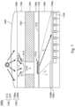
- FIG. 1 is a cross-sectional view of a spectrometer 1000 in accordance with some embodiments of the present disclosure.
- the spectrometer 1000 includes a plurality of photodetectors 1100 , an anti-reflection layer 1200 , a grating layer 1300 , a distant layer 1400 , and a collimator 1500 .
- the photodetector 1100 may be a Si photodetector, a Ge photodetector, or an organic photodetector.
- the plurality of photodetectors 1100 could be isolated by a plurality of deep trench insulation (DPI), as shown in FIG. 1 .
- DPI deep trench insulation
- the anti-reflection layer 1200 is disposed on the plurality of photodetectors 1100 .
- the anti-reflection layer 1200 is an anti-reflection coating (ARC) film.
- the anti-reflection layer 1200 is configured to increase the transmittance of the light L from the distant layer 1400 to the plurality of photodetectors 1100 .
- a refractivity of the anti-reflection layer is less than 15%.
- the material of the anti-reflection layer 1200 may include organic multi-film material or inorganic multi-film material, such as SiO 2 , SiH, or other suitable material.
- the grating layer 1300 is disposed above the anti-reflection layer 1200 and includes a plurality of grating structures 1310 to spread a light L into a spectrum to the plurality of photodetectors 1100 through a distant layer 1400 .
- the distant layer 1400 in FIG. 1 continuously extends from the grating layer 1300 (including the plurality of the grating structures 1310 and the grating substrate 1320 ) to the anti-reflection layer 1200 .
- the distant layer 1400 has a thickness T in a range from 400 ⁇ m to 2000 ⁇ m, such as 600, 800, 1000, 1200, 1400, 1600, or 1800 ⁇ m. If the thickness T of the distant layer 1400 is less than 400 ⁇ m, it may not provide a high resolution of the spectrometer 1000 . If the thickness T of the distant layer 1400 is greater than 2000 ⁇ m, it may not have the advantage of miniaturization of a high-resolution grating spectrometer on a chip.
- the distant layer 1400 having a thickness T at least 400 ⁇ m leads to the high-resolution spectrometer 1000 of the present disclosure.
- a refractive index of the distant layer 1400 is in a range from 1.5 to 2.2, such as 1.6, 1.8, or 2.0.
- the distant layer 1400 may be made from a low n polymer.
- a refractive index of the grating layer 1300 is greater than a refractive index of the distant layer 1400 .
- the collimator 1500 is disposed above the grating layer 1300 .
- the collimator 1500 is configured to confine an incident angle of the light L from a first micro-lens 1600 assuring the incident angle is around zero and increase a coupling efficiency of the light L from the grating layer 1300 to the plurality of photodetectors 1100 . In other words, the collimator 1500 could revise the light L to increase the coupling efficiency of image pixels.
- the pin hole 1510 of the collimator 1500 has a width W in a range from 0.1 to 10 ⁇ m, such as 0.5, 1, 2, 4, 6, or 8 ⁇ m. If the width W is smaller than 0.1 ⁇ m, it may not have sufficient amount of light transmitted into the grating layer 1300 below. If the width W is greater than 10 ⁇ m, the incident angle of the light L may be beyond a tolerance value, which leads to unexpected results of the optical resolution of the light L.
- the collimator 1500 illustrated in FIG. 2 A has three pin holes 1510 , the number of the pin hole 1510 is not limited in the present disclosure.
- the refractive index of the grating structures 1310 and a refractive index of the grating substrate 1320 may be the same or different.
- the refractive index of the grating structures 1310 and the refractive index of the grating substrate 1320 are in a range from 1.5 to 3.5, such as 1.8, 2.0, 2.2, 2.5, 2.8, 3.0, or 3.2.
- the grating structures 1310 and the grating substrate 1320 may be made from a high n polymer, such as SiNx, NbOx, TaOx, TiOx, SiHx.
- the material of the grating structures 1310 and the grating substrate 1320 may be the same (please refer to FIG. 8 E ) or different (please refer to FIG. 1 and FIG. 9 B ).
- the various grating structures 1310 of the grating layer 1300 will be described in detail in FIG. 5 A to FIG. 5 D below.
- FIG. 2 B is a top view of the plurality of grating structures 1310 of the spectrometer 1000 in FIG. 1 .
- the pin holes 1510 of the collimator 1500 are aligned with the grating structures 1310 of the grating layer 1300 .
- the vertical layout of the pin holes 1510 of the collimator 1500 could prevent T ⁇ 1 diffraction light and/or high order diffraction light from propagating into the grating layer 1300 below the collimator 1500 .
- the vertical layout of the grating structures 1310 could prevent T ⁇ 1 diffraction light and/or high order diffraction light from propagating into the distant layer 1400 below the grating structures 1310 .
- the spectrometer 1000 further includes a buffer layer 1700 , a cladding layer 1800 , and an absorption layer 1900 .
- the buffer layer 1700 is disposed between the first micro-lens 1600 and the collimator 1500 .
- a refractive index of the buffer layer 1700 is in a range from 1.5 to 2.2, such as 1.6, 1.8, or 2.0.
- the material of the buffer layer 1700 may be an organic material or inorganic material.
- the light transmittance of the buffer layer 1700 is greater than 80%.
- the cladding layer 1800 is disposed between the collimator 1500 and the grating layer 1300 . Specifically, the cladding layer 1800 is disposed on the grating layer 1300 .
- the refractive index of the grating layer 1300 is greater than a refractive index of the cladding layer 1800 .
- the refractive index of the grating structures 1310 of the grating layer 1300 is greater than the refractive index of the cladding layer 1800 .
- the refractive index of the cladding layer 1800 is in a range from 1.5 to 2.2, such as 1.6, 1.8, or 2.0.
- the absorption layer 1900 in FIG. 1 is disposed in the anti-reflection layer 1200 and is disposed under the grating structures 1310 .
- the absorption layer 1900 is disposed aside the plurality of photodetectors 1100 .
- the absorption layer 1900 is configured to absorb a zero order (T 0 ) diffraction light, thereby avoiding T 0 diffraction light passing to the plurality of photodetectors 1100 .
- the T 0 diffraction light herein is optical noise.
- the absorption coefficient K of the absorption layer 1900 is greater than 0.1.
- the anti-reflection layer 1200 is a conformal coating on the absorption layer 1900 and the plurality of photodetectors 1100 , and so a thickness of a first portion 1200 a of the anti-reflection layer 1200 over the plurality of photodetectors 1100 is substantially the same as a thickness of a second portion 1200 b of the anti-reflection layer 1200 over the absorption layer 1900 .
- the absorption layer 1900 may be made from metal or other absorption material.
- FIG. 3 is a partial view of the grating layer 1300 , the distant layer 1400 , the collimator 1500 , and the cladding layer 1800 of the spectrometer 1000 in FIG. 1 .
- the light L passes through the pin hole 1510 of the collimator 1500 , the light L passes through the cladding layer 1800 and propagates from the grating structures 1310 and the grating substrate 1320 of the grating layer 1300 into the distant layer 1400 .
- the light L has a critical angle ⁇ c between the grating substrate 1320 and the distant layer 1400 .
- an incident angle ⁇ T2 of a second order (T 2 ) diffraction light is greater than the critical angle ⁇ c , so that the T 2 diffraction light will occur TIR to filter out the T 2 diffraction light.
- the critical angle ⁇ c is in a range from 22 to 50 degrees, for example, 22.62 to 50 degrees.
- the refractive index of the grating structures 1310 is greater than the refractive index of the distant layer 1400 . The more the difference between the refractive index of the grating structures 1310 and the refractive index of the distant layer 1400 , the coupling efficiency of the grating structures 1310 to the distant layer 1400 would be better.
- ⁇ is a wavelength range of the light L
- ⁇ L is a length difference between a length L 1 and a length L 2 .
- the length L 1 equals T ⁇ tan( ⁇ 1 )
- the length L 2 equals T ⁇ tan( ⁇ 2 )
- the thickness T is a thickness of the distant layer 1400
- a emergent angle (diffraction angle) ⁇ 1 and a emergent angle (diffraction angle) ⁇ 2 respectively are minimum and maximum emergent angles of the light L. More specifically, a range that the length difference between the length L 1 and the length L 2 could be received by the light L spreading into a spectrum to the plurality of photodetectors 1100 .
- the optical resolution would be about
- Table 1 shows examples of the optical resolutions of the light L in various wavelength ranges and various thicknesses T of the distant layer 1400 .
- the thickness T of the distant layer 1400 in a range from 400 ⁇ m to 2000 ⁇ m.
- ⁇ is in a range from 300 nm to 600 nm
- ⁇ 1 and ⁇ 2 ranges from 22.62° to 50.29°
- the resulted optical resolution of the light L is in a range from 0.317 nm/ ⁇ m to 0.97 nm/ ⁇ m.
- ⁇ is in a range from 500 nm to 900 nm, ⁇ 1 and ⁇ 2 ranges from 22.62° to 43.81°, and the resulted optical resolution of the light L is in a range from 0.61 nm/ ⁇ m to 1.83 nm/ ⁇ m. In some embodiments, ⁇ is in a range from 800 nm to 1200 nm, ⁇ 1 and ⁇ 2 ranges from 23.58° to 36.87°, and the resulted optical resolution of the light L is in a range from 1.06 nm/ ⁇ m to 3.2 nm/ ⁇ m.
- FIG. 5 A to FIG. 5 D are enlargement views of various grating structures 1310 of the grating layer 1300 of the spectrometer 1000 in FIG. 1 .
- the binary grating structure 1310 a includes a first vertical sidewall SW 1 , a second vertical sidewall SW 2 , and a first top surface S 1 .
- the first vertical sidewall SW 1 is substantially parallel to the second vertical sidewall SW 2
- the first vertical sidewall SW 1 is substantially perpendicular to the first top surface S 1
- the second vertical sidewall SW 2 is substantially perpendicular to the first top surface S 1 .
- the binary grating structure 1310 a has a width W, a height H, and a period P, in which the period P is defined by a distance between two binary grating structures 1310 a .
- the period P is in a range from 0.25 to 0.4 ⁇ m, such as 0.3, or 0.35 ⁇ m.
- the height H is in a range from 0.25 to 0.4 ⁇ m, such as 0.3 ⁇ m.
- the binary grating structures 1310 a include different periods P, but have the same height H.
- the step grating structure 1310 b includes a third vertical sidewall SW 3 , a fourth vertical sidewall SW 4 , a fifth vertical sidewall SW 5 , a sixth vertical sidewall SW 6 , a second top surface S 2 , a third top surface S 3 , and a fourth top surface S 4 .
- the third vertical sidewall SW 3 , the fourth vertical sidewall SW 4 , the fifth vertical sidewall SW 5 , and the sixth vertical sidewall SW 6 are substantially parallel to each other.
- the second top surface S 2 , the third top surface S 3 , and the fourth top surface S 4 are substantially perpendicular to the fourth vertical sidewall SW 4 , the fifth vertical sidewall SW 5 , and the sixth vertical sidewall SW 6 .
- a step number of the step grating structures 1310 b is greater than 3.
- the step grating structures 1310 b include different periods P, but have the same height H.
- the blazed grating structure 1310 c includes a seventh vertical sidewall SW 7 and an eighth sidewall SW 8 .
- the eighth sidewall SW 8 is an inclined sidewall.
- the seventh vertical sidewall SW 7 and the eighth sidewall SW 8 form an angle.
- the blazed grating structures 1310 c include different periods P, but have the same height H.
- the slanted grating structure 1310 d includes a ninth sidewall SW 9 , a tenth sidewall SW 10 , and a fifth top surface S 5 .
- the ninth sidewall SW 9 and the tenth sidewall SW 10 are inclined sidewalls.
- the slanted grating structure 1310 d has a height H. In some embodiments, the height H is 0.5 ⁇ m.
- the fifth top surface S 5 connects to the ninth sidewall SW 9 and the tenth sidewall SW 10 .
- FIG. 6 is an enlargement view of the slanted grating structure 1310 d of the spectrometer 1000 in FIG. 1 .
- the slanted grating structure 1310 d is defined by the ninth sidewall SW 9 , the tenth sidewall SW 10 , and the fifth top surface S 5 .
- the ninth sidewall SW 9 , the tenth sidewall SW 10 , and the fifth top surface S 5 are defined by a bottom left point BL, a bottom right point BR, an upper left point UL, and an upper right point UR.
- the ninth sidewall SW 9 and a surface 1322 of the slanted grating structure 1310 d forms a bottom angle BA, and the tenth sidewall SW 10 and the surface 1322 of the slanted grating structure 1310 d forms a front angle FA.
- the coupling efficiency of the slanted grating structure 1310 d is between 60% and 90% in the T 1 diffraction light and a spectral range of 300 ⁇ 600 nm with the optical resolution of
- the slanted grating structures 1310 d include different periods P, but have the same slanted angles (such as the bottom angle BA and front angle FA).
- Each of the grating structures 1310 includes the binary grating structure 1310 a , the step grating structure 1310 b , the blazed grating structure 1310 c , or the slanted grating structure 1310 d .
- the grating structures 1310 illustrated in FIG. 1 could be substituted by the grating structures 1310 a - 1310 d illustrated in FIG. 5 A to FIG. 5 D . It is understood that the higher the order of the diffraction light, the greater the diffraction angle.
- the high order of the diffraction light (such as T 2 diffraction light, T 3 diffraction light, and so on) would be filtered by changing the width W, the height H, and/or the period P of the grating structures 1310 .
- the light L having a wavelength in a range from 300 nm to 600 nm diffracts into the distant layer 1400 when the grating structures 1310 have a period around 0.4 ⁇ m ⁇ 0.01 ⁇ m.
- the light L having a wavelength in a range from 500 nm to 900 nm diffracts into the distant layer 1400 when the grating structures 1310 have a period around 0.65 ⁇ m ⁇ 0.01 ⁇ m.
- the light L having a wavelength in a range from 800 nm to 1200 nm diffracts into the distant layer 1400 when the grating structures 1310 have a period around 0.9 ⁇ m ⁇ 0.01 ⁇ m.
- the thickness T of the distant layer 1400 could be adjusted by the incident angle ⁇ T1 of T 1 diffraction light transmitted out from the grating substrate 1320 .
- each of the grating structures 1310 a - 1310 d illustrated in FIG. 5 A to FIG. 5 D has three grating structures 1310 a - 1310 d
- the number of the grating structures 1310 a - 1310 d is not limited in the present disclosure.
- the grating structures 1310 a - 1310 d could be mirror structures in a lateral symmetry of FIG. 5 A to FIG. 5 D .
- the grating structures 1310 (including the binary grating structure 1310 a , the step grating structure 1310 b , the blazed grating structure 1310 c , or the slanted grating structure 1310 d ) could include multiple periods for multiple wavelength regions.
- the wavelength regions may cover 300 nm to 1200 nm. Therefore, the spectrometer 1000 of the present disclosure could cover a wide spectral range.
- FIG. 7 is a cross-sectional view of a spectrometer 1000 a in accordance with other embodiments of the present disclosure.
- the spectrometer 1000 in FIG. 1 further includes a second micro-lens 1610 to form the spectrometer 1000 a in FIG. 7 .
- the second micro-lens 1610 is configured to confine the incident angle of the light L and increase the light L entering into the grating structures 1310 .
- the incident angle of the light L is in a range between 0 and ⁇ 3 degrees, such as 0.5, 1, 1.5, 2, or 2.5 degrees.
- the incident angle of the light L is 0 degree.
- the second micro-lens 1610 is aligned with the pin hole 1510 of the collimator 1500 , and a second light-receiving surface 1612 of the second micro-lens 1610 is a concave surface.
- a second light-receiving surface 1612 of the second micro-lens 1610 is a concave surface.
- FIG. 8 A to FIG. 8 E are cross-sectional views of various stages of manufacturing a spectrometer in accordance with some embodiments of the present disclosure. It is understood that additional operations can be provided before, during, and after processes shown by FIG. 8 A to FIG. 8 E , and some of the operations described below can be replaced or eliminated, for additional embodiments of the process. The order of the operations/processes may be interchangeable.
- a substrate 2000 is provided, and the anti-reflection layer 1200 is deposited on the substrate 2000 .
- the substrate 2000 could include the plurality of photodetectors 1100 and the plurality of deep trench insulation (DPI) between the photodetectors 1100 .
- the anti-reflection layer 1200 could be formed by depositing multiple films of anti-reflection material, and the deposition method could be physical vapor deposition (PVD).
- the distant layer 1400 is taped on the anti-reflection layer 1200 .
- the grating layer 1300 (including the grating structures 1310 and the grating substrate 1320 ) is disposed on the distant layer 1400 .
- the grating layer 1300 in FIG. 8 C has undergone coating, exposure, development, and etching processes.
- the cladding layer 1800 is disposed on the grating layer 1300 .
- the cladding layer 1800 in FIG. 8 D has undergone coating and backing processes.
- the collimator 1500 with the pin hole 1510 aligned with the grating structures 1310 is disposed on the cladding layer 1800 .
- the collimator 1500 in FIG. 8 E has undergone coating, exposure, and development processes. It is noticed that the grating structures 1310 and the grating substrate 1320 of the grating layer 1300 in FIG. 8 E are formed by the same material.
- FIG. 9 A and FIG. 9 B are cross-sectional views of other examples of spectrometers in accordance with some embodiments of the present disclosure. Specifically, in FIG. 9 A , the grating substrate 1320 has been completely removed, thereby remaining the grating structures 1310 on the distant layer 1400 . In FIG. 9 B , the grating structures 1310 and the grating substrate 1320 of the grating layer 1300 are formed by different material.
- the spectrometer of the present disclosure includes a distant layer having a thickness at least 400 ⁇ m, and the spectrometer has the advantages of a miniaturized size, high resolution of the analysis results, readily integrated with complementary metal-oxide-semiconductor (CMOS) electronics, capable of covering a wide spectral range.
- CMOS complementary metal-oxide-semiconductor
Landscapes
- Physics & Mathematics (AREA)
- Spectroscopy & Molecular Physics (AREA)
- General Physics & Mathematics (AREA)
- Optics & Photonics (AREA)
- Spectrometry And Color Measurement (AREA)
- Other Investigation Or Analysis Of Materials By Electrical Means (AREA)
- Analysing Materials By The Use Of Radiation (AREA)
Abstract
Description
where Δλ is a wavelength range of the light, ΔL is a length difference between L1 and L2, where L1 equals T×tan(θ1), L2 equals T×tan(θ2), T is the thickness of the distant layer, and θ1 and θ2 respectively are minimum and maximum emergent angles of the light.
where Δλ is a wavelength range of the light L, ΔL is a length difference between a length L1 and a length L2. The length L1 equals T×tan(θ1), the length L2 equals T×tan(θ2), the thickness T is a thickness of the
of the
With the similar calculation method mentioned above, the light L having a wavelength in a range from 500 nm to 900 nm and the thickness T of the
The light L having a wavelength in a range from 800 nm to 1200 nm, the optical resolution would be about
| TABLE 1 | |||
| wavelength | 300 nm~600 nm | 500 nm~900 nm | 800 nm~1200 nm |
| diffraction | 300 nm | 500 nm | 800 nm |
| angle | @θ1 = 22.62°, | @θ1 = 22.62°, | @θ1 = 23.58° |
| 600 nm | 900 |
1200 nm | |
| @θ2 = 50.29° | @θ2 = 43.81° | @θ2 = 36.87° | |
| distant layer | 0.97 nm/μm | 1.83 nm/μm | 3.2 nm/μm |
| T = 400 μm | |||
| distant layer | 0.63 nm/μm | 1.22 nm/μm | 2.12 nm/μm |
| T = 600 μm | |||
| distant layer | 0.47 nm/μm | 0.92 nm/μm | 1.59 nm/μm |
| T = 800 μm | |||
| distant layer | 0.317 nm/μm | 0.61 nm/μm | 1.06 nm/μm |
| T = 1200 μm | |||
for the
Claims (20)
Priority Applications (2)
| Application Number | Priority Date | Filing Date | Title |
|---|---|---|---|
| US17/824,635 US12123776B2 (en) | 2022-05-25 | 2022-05-25 | Spectrometer |
| TW111136668A TWI808014B (en) | 2022-05-25 | 2022-09-28 | Miniaturization of spectrometer on chip |
Applications Claiming Priority (1)
| Application Number | Priority Date | Filing Date | Title |
|---|---|---|---|
| US17/824,635 US12123776B2 (en) | 2022-05-25 | 2022-05-25 | Spectrometer |
Publications (2)
| Publication Number | Publication Date |
|---|---|
| US20230408335A1 US20230408335A1 (en) | 2023-12-21 |
| US12123776B2 true US12123776B2 (en) | 2024-10-22 |
Family
ID=88149182
Family Applications (1)
| Application Number | Title | Priority Date | Filing Date |
|---|---|---|---|
| US17/824,635 Active 2043-02-28 US12123776B2 (en) | 2022-05-25 | 2022-05-25 | Spectrometer |
Country Status (2)
| Country | Link |
|---|---|
| US (1) | US12123776B2 (en) |
| TW (1) | TWI808014B (en) |
Citations (13)
| Publication number | Priority date | Publication date | Assignee | Title |
|---|---|---|---|---|
| US20010015850A1 (en) * | 1998-12-18 | 2001-08-23 | Marek W. Kowarz | Multilevel mechanical grating device |
| TW200602674A (en) | 2004-07-09 | 2006-01-16 | Hon Hai Prec Ind Co Ltd | Grating spectrograph |
| US20070070347A1 (en) | 2005-06-08 | 2007-03-29 | Axel Scherer | Method and apparatus for CMOS imagers and spectroscopy |
| CN103698010A (en) | 2013-12-31 | 2014-04-02 | 中国科学院光电研究院 | Miniaturized linear variable filter type imaging spectrometer |
| US20140092384A1 (en) * | 2011-05-19 | 2014-04-03 | Hitachi High-Technologies Corporation | Diffraction grating manufacturing method, spectrophotometer, and semiconductor device manufacturing method |
| TW201414992A (en) | 2012-07-17 | 2014-04-16 | Heptagon Micro Optics Pte Ltd | Compact spectrometer module and manufacturing method thereof |
| US20200064195A1 (en) * | 2018-08-27 | 2020-02-27 | Csem Centre Suisse D'electronique Et De Microtechnique Sa - Recherche Et Developpement | Optical filter, optical filter system, spectrometer and method of fabrication thereof |
| US20200363323A1 (en) * | 2017-11-21 | 2020-11-19 | CSEM Centre Suisse d'Electronique et de Microtechnique SA - Recherche et Développement | Spectrometer |
| WO2021058259A1 (en) | 2019-09-26 | 2021-04-01 | Robert Bosch Gmbh | Miniaturised spectrometer device and method for producing a miniaturised spectrometer device |
| WO2021070305A1 (en) * | 2019-10-09 | 2021-04-15 | 日本電信電話株式会社 | Spectral element array, imaging element, and imaging device |
| US20210311226A1 (en) * | 2018-08-02 | 2021-10-07 | Rensselaer Polytechnic Institute | Zero-index photonic crystals for visible and near infrared applications |
| US20220019015A1 (en) * | 2020-07-14 | 2022-01-20 | Facebook Technologies, Llc | Inorganic matrix nanoimprint lithographs and methods of making thereof |
| US11333811B1 (en) * | 2020-12-23 | 2022-05-17 | Viavi Solutions Inc. | Optical device |
-
2022
- 2022-05-25 US US17/824,635 patent/US12123776B2/en active Active
- 2022-09-28 TW TW111136668A patent/TWI808014B/en active
Patent Citations (14)
| Publication number | Priority date | Publication date | Assignee | Title |
|---|---|---|---|---|
| US20010015850A1 (en) * | 1998-12-18 | 2001-08-23 | Marek W. Kowarz | Multilevel mechanical grating device |
| TW200602674A (en) | 2004-07-09 | 2006-01-16 | Hon Hai Prec Ind Co Ltd | Grating spectrograph |
| US20070070347A1 (en) | 2005-06-08 | 2007-03-29 | Axel Scherer | Method and apparatus for CMOS imagers and spectroscopy |
| US20140092384A1 (en) * | 2011-05-19 | 2014-04-03 | Hitachi High-Technologies Corporation | Diffraction grating manufacturing method, spectrophotometer, and semiconductor device manufacturing method |
| TW201414992A (en) | 2012-07-17 | 2014-04-16 | Heptagon Micro Optics Pte Ltd | Compact spectrometer module and manufacturing method thereof |
| CN103698010A (en) | 2013-12-31 | 2014-04-02 | 中国科学院光电研究院 | Miniaturized linear variable filter type imaging spectrometer |
| US20200363323A1 (en) * | 2017-11-21 | 2020-11-19 | CSEM Centre Suisse d'Electronique et de Microtechnique SA - Recherche et Développement | Spectrometer |
| US20210311226A1 (en) * | 2018-08-02 | 2021-10-07 | Rensselaer Polytechnic Institute | Zero-index photonic crystals for visible and near infrared applications |
| US20200064195A1 (en) * | 2018-08-27 | 2020-02-27 | Csem Centre Suisse D'electronique Et De Microtechnique Sa - Recherche Et Developpement | Optical filter, optical filter system, spectrometer and method of fabrication thereof |
| CN110865431A (en) | 2018-08-27 | 2020-03-06 | 瑞士Csem电子显微技术研发中心 | Optical filter, optical filter system, spectrometer and manufacturing method thereof |
| WO2021058259A1 (en) | 2019-09-26 | 2021-04-01 | Robert Bosch Gmbh | Miniaturised spectrometer device and method for producing a miniaturised spectrometer device |
| WO2021070305A1 (en) * | 2019-10-09 | 2021-04-15 | 日本電信電話株式会社 | Spectral element array, imaging element, and imaging device |
| US20220019015A1 (en) * | 2020-07-14 | 2022-01-20 | Facebook Technologies, Llc | Inorganic matrix nanoimprint lithographs and methods of making thereof |
| US11333811B1 (en) * | 2020-12-23 | 2022-05-17 | Viavi Solutions Inc. | Optical device |
Non-Patent Citations (1)
| Title |
|---|
| English Translation of Miyata et al WO2021070305A1 Description (Year: 2021). * |
Also Published As
| Publication number | Publication date |
|---|---|
| TWI808014B (en) | 2023-07-01 |
| US20230408335A1 (en) | 2023-12-21 |
| TW202346788A (en) | 2023-12-01 |
Similar Documents
| Publication | Publication Date | Title |
|---|---|---|
| US9683894B2 (en) | Spectroscopic sensor and electronic apparatus | |
| KR102716652B1 (en) | Optical device | |
| US20240304645A1 (en) | Spectrum chip and manufacturing method therefor, and spectrum analysis device | |
| US20140092385A1 (en) | Dispersed fourier transform spectrometer, methods and systems | |
| KR102832511B1 (en) | Spectrophotometer array, imaging device and imaging device | |
| US8570510B2 (en) | Optical unit | |
| US10566377B2 (en) | Self-aligned optical grid on image sensor | |
| KR20210020469A (en) | Spectral camera | |
| KR20190058131A (en) | Fourier-transform interferometer using metasurface | |
| JPH06229829A (en) | Photoreceptor element array | |
| US12123776B2 (en) | Spectrometer | |
| US20260016336A1 (en) | Integrated chirped-grating spectrometer-on-a-chip | |
| US10451821B2 (en) | Photonic circuit light coupler | |
| US20170146707A1 (en) | Spectral device and image-pickup device | |
| TWI759153B (en) | Fingerprint sensing module | |
| CN114420714A (en) | On-chip integrated spectrometer, manufacturing method thereof and electronic equipment | |
| US9429471B2 (en) | Photodiode array for spectrometric measurements and spectrometric measurement system | |
| US11841270B1 (en) | Spectrometer | |
| EP2331920B1 (en) | Integrated circuit with grating and manufacturing method therefor | |
| CN115719753A (en) | Spectrum chip, preparation method thereof and spectrum analysis device | |
| TW201416648A (en) | Spectrometer and optical module thereof | |
| US12364042B2 (en) | Optical element having both color filter function and lens function, image sensor thereof and imaging device | |
| TW201350813A (en) | Diffraction grating devices, spectroscopes, and spectroscopy systems |
Legal Events
| Date | Code | Title | Description |
|---|---|---|---|
| AS | Assignment |
Owner name: VISERA TECHNOLOGIES COMPANY LTD., TAIWAN Free format text: ASSIGNMENT OF ASSIGNORS INTEREST;ASSIGNORS:SHIH, WEN-YU;HSIEH, HSIN-YI;LAI, LAI-HUNG;AND OTHERS;SIGNING DATES FROM 20220422 TO 20220426;REEL/FRAME:060018/0235 |
|
| FEPP | Fee payment procedure |
Free format text: ENTITY STATUS SET TO UNDISCOUNTED (ORIGINAL EVENT CODE: BIG.); ENTITY STATUS OF PATENT OWNER: LARGE ENTITY |
|
| STPP | Information on status: patent application and granting procedure in general |
Free format text: DOCKETED NEW CASE - READY FOR EXAMINATION |
|
| STPP | Information on status: patent application and granting procedure in general |
Free format text: NON FINAL ACTION MAILED |
|
| STPP | Information on status: patent application and granting procedure in general |
Free format text: RESPONSE TO NON-FINAL OFFICE ACTION ENTERED AND FORWARDED TO EXAMINER |
|
| STPP | Information on status: patent application and granting procedure in general |
Free format text: NOTICE OF ALLOWANCE MAILED -- APPLICATION RECEIVED IN OFFICE OF PUBLICATIONS |
|
| STPP | Information on status: patent application and granting procedure in general |
Free format text: PUBLICATIONS -- ISSUE FEE PAYMENT VERIFIED |
|
| STCF | Information on status: patent grant |
Free format text: PATENTED CASE |