EP2705570B1 - Vorrichtung zum empfangen und/oder senden einer welle, system mit dieser vorrichtung und verwendung dieser vorrichtung - Google Patents
Vorrichtung zum empfangen und/oder senden einer welle, system mit dieser vorrichtung und verwendung dieser vorrichtung Download PDFInfo
- Publication number
- EP2705570B1 EP2705570B1 EP11779214.3A EP11779214A EP2705570B1 EP 2705570 B1 EP2705570 B1 EP 2705570B1 EP 11779214 A EP11779214 A EP 11779214A EP 2705570 B1 EP2705570 B1 EP 2705570B1
- Authority
- EP
- European Patent Office
- Prior art keywords
- resonant elements
- passive
- active
- elements
- band
- Prior art date
- Legal status (The legal status is an assumption and is not a legal conclusion. Google has not performed a legal analysis and makes no representation as to the accuracy of the status listed.)
- Active
Links
Images


Classifications
-
- H—ELECTRICITY
- H01—ELECTRIC ELEMENTS
- H01Q—ANTENNAS, i.e. RADIO AERIALS
- H01Q15/00—Devices for reflection, refraction, diffraction or polarisation of waves radiated from an antenna, e.g. quasi-optical devices
- H01Q15/0006—Devices acting selectively as reflecting surface, as diffracting or as refracting device, e.g. frequency filtering or angular spatial filtering devices
- H01Q15/006—Selective devices having photonic band gap materials or materials of which the material properties are frequency dependent, e.g. perforated substrates, high-impedance surfaces
-
- H—ELECTRICITY
- H01—ELECTRIC ELEMENTS
- H01Q—ANTENNAS, i.e. RADIO AERIALS
- H01Q1/00—Details of, or arrangements associated with, antennas
- H01Q1/40—Radiating elements coated with or embedded in protective material
-
- H—ELECTRICITY
- H01—ELECTRIC ELEMENTS
- H01Q—ANTENNAS, i.e. RADIO AERIALS
- H01Q3/00—Arrangements for changing or varying the orientation or the shape of the directional pattern of the waves radiated from an antenna or antenna system
- H01Q3/44—Arrangements for changing or varying the orientation or the shape of the directional pattern of the waves radiated from an antenna or antenna system varying the electric or magnetic characteristics of reflecting, refracting, or diffracting devices associated with the radiating element
- H01Q3/446—Arrangements for changing or varying the orientation or the shape of the directional pattern of the waves radiated from an antenna or antenna system varying the electric or magnetic characteristics of reflecting, refracting, or diffracting devices associated with the radiating element the radiating element being at the centre of one or more rings of auxiliary elements
Definitions
- the present invention concerns a device for receiving and/or emitting an electromagnetic wave, a system comprising said device, and a use of such device.
- a device for receiving and/or emitting an electromagnetic wave comprising a plurality of passive reflective elements.
- the passive reflective elements are periodically spaced inside the device, and said device uses specific Bragg law electromagnetic properties.
- the passive reflective elements are spaced from each other of a distance that is a multiple of the wavelength ⁇ .
- the distance is about ⁇ /2 or greater and such device has a large size.
- Such device does not have a preferred direction for the electromagnetic wave.
- One object of the present invention is to provide an improved device for receiving and/or emitting an electromagnetic wave.
- the present invention proposes a device receiving and/or emitting an electromagnetic wave having a free space wavelength ⁇ 0 comprised between 1 mm and 10 m, comprising:
- the device for receiving and/or emitting an electromagnetic wave is small compared to the equivalent known devices of the prior art.
- the passive resonant elements are coupled to each others, and the device does not use the Bragg law: the passive resonant elements can be periodic or non periodic inside the medium.
- the device uses a band-gap that is known as an hybridization band-gap.
- a first region of the device comprising the passive resonant elements is preventing a propagation of electromagnetic waves at the second resonance frequency from the active resonant element through said first region.
- the device comprises a directivity diagram that is determined by the shape of said first region.
- the device is able to emit and/or receive an electromagnetic wave according to one or a plurality of predetermined directions.
- the electromagnetic energy at the second resonance frequency is concentrated inside a second region around the active resonant element.
- the device is able to emit and/or receive an electromagnetic wave at a greater distance from itself.
- the device has a greater sensitivity and is more efficient.
- one and/or other of the following features may optionally be incorporated.
- the second shape is identical to said first shape, and at least one of the second physical parameters of the second structure is different to a corresponding first physical parameter of the first structure.
- the first and second physical parameters comprise sizes and materials of the first and second structure, respectively.
- the first distance and the second distance are lower than ⁇ /10.
- the passive resonant elements are not periodically disposed inside the medium.
- the active resonant element is in proximity of a lateral surface of the medium.
- the active resonant element is at a third distance from the lateral surface, said third distance being lower than the wavelength ⁇ .
- the device further comprises at least two active resonant elements, said two active resonant elements being separated from each other of a forth distance, and wherein said two active resonant elements have different second resonance frequencies, each of them being comprised inside said band-gap.
- the two active resonant elements can therefore emit independent and uncorrelated electromagnetic waves.
- the forth distance is lower than the wavelength ⁇ , and preferably lower than ⁇ /4.
- the forth distance is adapted so that at least one passive resonant element is substantially between said two active resonant elements.
- the two active resonant elements are positioned symmetrically in comparison to a geometrical centre of said device.
- the device further comprises:
- the two active resonant elements can therefore emit independent and uncorrelated electromagnetic waves.
- the device further comprises:
- the two active resonant elements can therefore emit independent and uncorrelated electromagnetic waves.
- the first and second shapes are wires of electrical conductors, the first resonance frequency depending on a length of said first shape, and the second resonance frequency depending on a length of said second shape.
- the first and second shapes are split rings of electrical conductors, the first resonance frequency depending on an electric capacitor and an electric inductance of said first shape, and the second resonance frequency depending on an electric capacitor and an electric inductance of said second shape.
- the first and second shapes are slots on an electrical conductor plate, the first resonance frequency depending on a perimeter length of the slot of said first shape, and the second resonance frequency depending on a length of the slot of said second shape.
- Another object of the present invention is to provide a system comprising a device for receiving and/or emitting an electromagnetic wave, wherein the active resonant element is connected to an electronic device for receiving and/or emitting a signal representative to said electromagnetic wave, said electric signal having at least a frequency component substantially equal to the second frequency.
- Another object of the present invention is to use a device for receiving and/or emitting an electromagnetic wave having a free space wavelength ⁇ comprised between 1 mm and 1 m, and preferably between 10 cm and 40 cm.
- the direction Z is a vertical direction.
- a direction X or Y is a horizontal or lateral direction.
- Figure 1 shows a first embodiment of a device 10 for receiving or emitting an electromagnetic wave W in a space and having a free space wavelength ⁇ 0 comprised between 1 mm and 10 m, and preferably between 10 cm and 40 cm.
- This device comprises:
- the medium 11 has a refractive index n d .
- the space may be air. In that case, its refractive index is equal to one.
- the medium 11 is for example a parallelepiped, comprising a first surface S1 and a second surface S2, the second surface S2 being opposite to said first surface along the vertical direction Z.
- the first and second surfaces S1, S2 are substantially parallel planes.
- a direction D is substantially a straight line perpendicular to said surfaces and parallel to the vertical direction Z.
- the first and second surfaces S1, S2 are distant of a height value H.
- the medium 11 has an electric permeability of ⁇ d .
- the passive resonant elements 12 have a first structure comprising at least a first shape and first physical parameters.
- the length Lw1 of each passive resonant element is for example equal to the height value H of the medium 11.
- each passive resonant element 12 of the first embodiment are electrical conductive wires having a diameter a and extending along the direction D according to a length Lw1 between a first end 12a above the first surface S1 and a second end 12b above second surface S2.
- the passive resonant elements 12 form on the first surface S1 or any plane XY perpendicular to said vertical direction Z a regularly spaced square grid.
- the passive resonant elements 12 are parallel to each other along the vertical direction Z.
- the passive resonant elements 12 have at least one resonance frequency f 1 , a first resonance frequency.
- the passive resonant elements 12 are spaced from each other along the direction X or Y of a first distance d1 lower than ⁇ /4, and preferably lower than ⁇ /10.
- This sub-wavelength first distance d1 is the step of said grid.
- the passive resonant elements 12 are therefore electromagnetically coupled to each other.
- a hybridization band-gap is created around the first resonance frequency f 1 .
- the band-gap will be above the resonance frequency of a single wire.
- the passive resonant elements 12 form on figure 1 a regular lattice of wires (periodically spaced). But, such device can be operational if the passive resonant elements 12 are not regularly and periodically spaced.
- Figures 5a to 5d represents a plurality of variants for the first shape of the passive resonant elements 12.
- the passive resonant elements 12 are composed of a single wire.
- the first resonance frequency f 1 depends on the length L w1 that is a curvilinear length between the first end 12a and the second end 12b.
- the length L w1 generates a plurality of first resonance frequencies f 1 , each of them being multiple of the first one. But, the present description will only refer to the first one of them for simplicity.
- the passive resonant elements 12 are composed of a main wire extending between the first end 12a and the second end 12b, connected to additional wires, for example one additional wire extending between an end 12d and an end 12c, the end 12d also belonging to the main wire and/or being connected to said main wire at an intermediate position between the main wire ends 12a, 12b.
- Such passive resonant element comprises a plurality of geometrical lengths:
- Each of these geometrical lengths L wi , i being an index representing a wire portion of the passive resonant element 12, is related to an electrical length L wi *, to a first resonance wavelength ⁇ 1i , and to a first resonance frequency f 1i .
- the passive resonant element 12 has a plurality of resonance frequencies f 1i that can be represented, for the plurality of all of them, in a wavenumber-frequency diagram as shown on figure 4 .
- a particular first frequency f 11 is given for a wavenumber k 1 .
- All the pairs (f 1i , k i ) that are available for the plurality of passive resonant elements 12 are represented on this diagram by a plurality of curves 21, 22.
- the scattering phenomenon forms asymptotes in this diagram and creates a frequency band-gap ⁇ f wherein the plurality of passive resonant elements 12 does not have any possibility for the propagation of an electromagnetic wave having a frequency f belonging to said band-gap ⁇ f, that is to say belonging to a frequency interval [f ⁇ 1 ,f ⁇ 2 ].
- the passive resonant elements 12 can be incorporated inside the medium 11 according to a periodic pattern.
- the device has a simple geometry, and the device electromagnetic properties (sensitivity, directivity, performance or efficiency) can be more easily computed and predicted before fabrication.
- the passive resonant elements 12 can be incorporated inside the medium 11 according to a non periodic pattern.
- the device is less sensitive to fabrication uncertainties concerning the positions of the passive resonant elements 12 inside the medium 11. Such problem is well known for Bragg band-gap materials or metamaterials.
- One or several active resonant elements 13 are also incorporated inside the medium 11 between the passive resonant elements 12.
- the active resonant elements 13 are coupled or connected to an electronic device 14 for receiving or emitting a signal.
- the active resonant elements 13 can be fed with a single electric signal S to emit or receive a single electromagnetic wave W, or they may be fed with a plurality of electric signals (one different signal for each active element) to emit or receive simultaneously the plurality of signals through a plurality of independent electromagnetic waves.
- the active resonant elements 13 are close to the passive resonant elements 12.
- the active resonant element 13 is spaced apart from a passive resonant element 12 belonging to the plurality of resonant passive elements of a second distance d2 that is lower than ⁇ /2, and eventually lower than ⁇ /10.
- the active resonant element 13 is preferably positioned inside the medium 11, in proximity of a periphery of said medium that is to say in proximity of lateral surface LS.
- the distance between the active resonant element 13 and the proximal lateral surface from said active resonant element is lower than a third distance d3.
- a third distance d3 Between said active resonant element 13 and said proximal lateral surface there is no or only one passive resonant element 12.
- the active resonant element 13 is therefore able to emit an electromagnetic wave W laterally from said lateral surface LS ( figures 1 and 2 ), said wave W propagating in space mainly according to plane XY.
- the third distance d3 is lower than the wavelength ⁇ , and preferably lower than ⁇ /4.
- the active resonant element 13 is near the proximal lateral surface LS.
- the active resonant element 13 is preferably at the periphery.
- the device has a small size.
- the active resonant element 13 has a second structure comprising a second shape and second physical parameters.
- the second shape of the active resonant element is identical to the first shape of the passive resonant element.
- the active resonant element 13 differs from the passive resonant element 12 only by the length L w2 that is shorter than the length L w1 .
- the passive and active resonant elements 12, 13 only differ by their physical parameters.
- the second structure of the active resonant element is therefore different to the first structure of the passive resonant element.
- the active resonant element 13 has a resonance frequency, named a second resonance frequency f 2 .
- the second resonance frequency f 2 is comprised between f ⁇ 1 and f ⁇ 2 , i.e. inside the band-gap ⁇ f of the plurality of passive resonant elements 12.
- the electrical length of the wire of the active resonant element 13 is for example reduced compared to the electrical length of the wire of the passive resonant element 12:
- the second resonance frequency f 2 of the active resonant element 13 is higher than the first frequency f1 of the passive resonant elements 12, and said second resonance frequency f 2 can fall inside the band-gap ⁇ f.
- the plurality of passive resonant elements 12 does not propagate waves belonging to said band-gap ⁇ f.
- An emitted wave W emitted form the active resonant element 13 is attenuated in the direction of the plurality of passive resonant elements 12.
- the device behaves such as having a first region R1 comprising most of the passive resonant elements 12, and a second region R2 comprising the active resonant elements 13, the first and second region R1, R2 excluding each other and being separated by a boundary 19 ( figure 2 ).
- the second region R2 around the active resonant elements 13 concentrates the electromagnetic energy coming from the active resonant element 13 and the first region R1 prevents the propagation of said energy through it.
- the device is therefore able to emit or to receive an electromagnetic wave W according to a predetermined direction or several predetermined directions, said predetermined directions being defined by the shapes of the first and second regions R1, R2.
- Figure 3 is an example of directivity diagram corresponding to one active resonant element 13 of the device shown on figure 2 . Such device has a clear directivity curve 30 oriented to the direction of 180°.
- the device can emit a different signal from each active resonant element 13 for a multi-input multi-output (MIMO) application.
- MIMO multi-input multi-output
- a signal having a frequency component substantially equal to the second frequency f 2 can be efficiently emitted or received.
- the device can emit or receive an electromagnetic wave in the far field, with an improved sensitivity compared with a device wherein the second frequency f 2 of the active resonant element 13 is not inside the band-gap ⁇ f of the plurality of passive resonant elements 12.
- the shapes of the active resonant elements 13 are preferably identical to the shape of the passive resonant element 12. At least one of the physical parameters of the active resonant elements 13 is different than physical parameters of the passive resonant elements 12.
- the active resonant element 13 can have a second resonance frequency f 2 inside the band-gap ⁇ f of the plurality of passive resonant elements 12.
- the device of figure 2 comprises four active resonant elements 13 1 , 13 2 , 13 3 , 13 4 , each of them emitting or receiving an electromagnetic wave W according to a different direction, for example according to a direction of each quadrant in the plane XY.
- the electric signals of the plurality of active resonant elements 13 can be different from each other. In case of reception, the electric signals of the plurality of active resonant elements 13 can be different and uncorrelated to each other.
- These active resonant elements 13 may be used independently from each other and may be used in a MIMO configuration of the device.
- This device comprising a plurality of active resonant elements 13 is an extremely compact array of antenna.
- two active resonant elements (13 1 , 13 2 ) are separated from each other of a forth distance d4.
- the forth distance d4 between two active resonant elements 13 is preferably higher than the second distance d2 between an active resonant element 13 and a neighbour passive resonant element 12. At least one passive resonant element 12 is for example between two active resonant elements 13. The active resonant elements 13 belonging to the plurality are not coupled to each other.
- the forth distance d4 is for example lower than the wavelength in the medium 11, and preferably lower than ⁇ /4.
- the device comprising a plurality of active resonant elements 13 is small.
- the electric signals of the plurality of active resonant elements 13 are therefore more uncorrelated to each other, so that they can be used independently.
- the two active resonant elements may also have different second physical parameters, so that the first active resonant element 13 1 has a second resonant frequency f 21 that is different than the second resonant frequency f 22 of the second active resonant element 13 2 .
- the two active resonant elements (13 1 , 13 2 ) are then not coupled to each other, and the signals of the active resonant elements 13 are again more uncorrelated.
- Figure 6 represents a variant of the first embodiment of the invention, wherein the shapes of passive and active resonant elements 12, 13 are folded wires.
- the passive resonant elements 12 are conductive wires of approximately 30 mm length, with first half portion in direction Z and second half portion in direction Y.
- the first resonance frequency f 1 corresponds to the above lengths of the passive resonant elements 12 conductive wires. In that case, the first resonance frequency f1 is approximately of 2.2 GHz.
- the active resonant element 13 is a conductive wire of approximately 25 mm length, with first portion in direction Z and second portion in direction Y above the second half portions of the passive resonant elements 12.
- the second resonance frequency f 2 corresponds to the above length of the active resonant element 13 conductive wire. In that case, the second resonance frequency f 2 is approximately of 2.45 GHz.
- the different portions of wires that are parallel to each other are distant of 2 mm.
- the device can then emit and receive wave at a central frequency of approximately 2.45 GHz corresponding to the second resonance frequency f 2 , and with a frequency bandwidth of approximately 100 MHz, said frequency bandwidth being comprised inside the frequency band-gap ( ⁇ f) of the passive resonant elements.
- the central frequency corresponds to a free space wavelength ⁇ 0 between 20 cm and 12 cm.
- the fist and second distances (d1, d3) are lower than ⁇ /10.
- the size of the device in the Y and Z directions of this variant is therefore smaller than in the device of figure 1 .
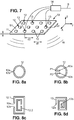
- Figure 7 shows a second embodiment of a device 10 for receiving or emitting an electromagnetic wave W comprising a plurality of passive resonant elements 12 and at least one active resonant element 13. These passive and active resonant elements have a different shape compared with those of the first embodiment.
- passive and active resonant elements 12, 13 are in the form of a split ring element extending in a plane XY above the first surface S1. Their structure also uses electrical conductive elements.
- Such second embodiment of the invention is smaller in the direction Z compared to the first embodiment of the invention.
- the first shape and the second shape are small loops having at least one opening, like a C letter.
- the loop behaves like an electric inductance L.
- the opening behaves like an electric capacitor C.
- the passive or active resonant element 12, 13 behaves like a small electric circuit having a resonance frequency f c that is substantially equal to 1 2 ⁇ LC .
- the passive resonant element 12 has a first resonance frequency f 1 depending on an electric capacitor C 1 and an electric inductance L 1 .
- the active resonant element 13 has a second resonance frequency f 2 depending on an electric capacitor C 2 and an electric inductance L 2 .
- the plurality of passive resonant elements 12 has a band-gap ⁇ f.
- the active resonant element 13 is designed to have a second resonance frequency inside the band-gap.
- Such device is small and efficient to emit or receive an electromagnetic wave W from or to far field.
- Figure 8a to 8d shows four variants of shapes for the passive or active elements 12, 13.
- the variants of figures 7c provide two different second resonance frequencies (f 21 , f 22 ).
- the two second resonance frequencies can be positioned inside the frequencies band-gap ⁇ f of the passive resonant elements 12.
- Figure 9 shows a third embodiment of a device 10 for receiving or emitting an electromagnetic wave W comprising a plurality of passive resonant elements 12 and at least one active resonant element 13.
- passive and active resonant elements have a different shape compared with those of the first embodiment: they are slots on an electrical conductor plate extending along a plane XY.
- the device of this third embodiment is smaller than the first and second ones.
- a first resonance frequency (f 1 ) depends on a perimeter length of the slot, and not a length of it. The perimeter is approximately twice longer than the length.
- the passive resonant elements 12 are slots in an electric conductive plate of 24 mm length and 0.5 mm width.
- the first resonance frequency f 1 corresponds to the above length and width (perimeter) of the passive resonant elements 12 slots. In that case, the first resonance frequency f1 is approximately of 2.2 GHz.
- the active resonant element 13 is a slot of 19 mm length and 0.5 mm width.
- the second resonance frequency f 2 corresponds to the above length and width of the active resonant element 13 slot. In that case, the second resonance frequency f 2 is approximately of 2.45 GHz.
- the slots are distant from each other of 2 mm.
- the device can then emit and receive wave at a central frequency of approximately 2.45 GHz corresponding to the second resonance frequency f 2 , and with a frequency bandwidth of approximately 100 MHz, said frequency bandwidth being comprised inside the frequency band-gap ( ⁇ f) of the passive resonant elements.
- the fist and second distances (d1, d3) are also lower than ⁇ /10.
- This device in Y direction is twice lower than the size of figure 6 . Such device is smaller.
- the device for receiving and/or emitting an electromagnetic wave is small compared to the equivalent known devices of the prior art.
- Such device has a high efficiency to emit or receive an electromagnetic wave, so that data can be transmitted to a great distance from the device.
- the device can be designed to provide a predetermined directivity diagram that is determined by the first and second region shapes (region with passive resonant elements and region with active resonant element).
- the device can comprise a plurality of active resonant elements that are isolated from each other by the passive resonant elements 12 band-gap.
- the device can be used for MIMO application with very low correlation between the channels.
Landscapes
- Physics & Mathematics (AREA)
- Optics & Photonics (AREA)
- Aerials With Secondary Devices (AREA)
- Details Of Aerials (AREA)
- Waveguide Connection Structure (AREA)
- Variable-Direction Aerials And Aerial Arrays (AREA)
Claims (17)
- Vorrichtung (10), die dafür konfiguriert ist, eine elektromagnetische Welle zu empfangen und/oder zu senden, die eine Freiraumwellenlänge λ0 im Bereich zwischen 1 mm und 10 m aufweist, umfassend:- eine elektronische Vorrichtung (14), die dafür konfiguriert ist, ein Signal (S) zu empfangen oder zu senden,- ein Medium (11) aus dielektrischem Material, wobei die Freiraumwellenlänge λ0 einer Wellenlänge A innerhalb des Mediums (11) entspricht,- eine Vielzahl von passiven Resonanzelementen (12), die in dem Medium beinhaltet sind, wobei jedes passive Resonanzelement (12) eine erste Struktur aufweist, die mindestens eine erste Form und erste physikalische Parameter umfasst, wobei die erste Struktur bei allen den passiven Resonanzelementen, die zu der Vielzahl von passiven Resonanzelementen (12) gehören, die gleiche ist, wobei jedes passive Resonanzelement (12) mindestens eine erste Resonanzfrequenz (f1) aufweist, wobei die Vielzahl von passiven Resonanzelementen (12) eine Frequenzbandlücke (Δf) umfassen, wobei zwei benachbarte passive Resonanzelemente, die zu der Vielzahl gehören, um einen ersten Abstand (d1) voneinander beabstandet sind, der kleiner ist als λ/4,- mindestens ein aktives Resonanzelement (13), das in der Vielzahl von passiven Resonanzelementen (12) beinhaltet ist, wobei das aktive Resonanzelement (13) eine zweite Struktur aufweist, die mindestens eine zweite Form und zweite physikalische Parameter umfasst, wobei sich die zweite Struktur so von der ersten Struktur unterscheidet, dass das aktive Resonanzelement (13) mindestens eine zweite Resonanzfrequenz (f2) aufweist, die in der Frequenzbandlücke (Δf) der Vielzahl von passiven Elementen (12) umfasst ist, wobei das aktive Resonanzelement (13) mit der elektronischen Vorrichtung (14) verbunden ist, um ein Signal (S) zu empfangen oder zu senden, das mindestens eine Frequenzkomponente aufweist, die im Wesentlichen mit der zweiten Frequenz (f2) gleich ist,dadurch gekennzeichnet, dass das aktive Resonanzelement (13) von einem benachbarten passiven Resonanzelement um einen zweiten Abstand (d2) beabstandet ist, der kleiner ist als λ/4.
- Vorrichtung nach Anspruch 1, wobei die zweite Form mit der ersten Form identisch ist, und sich mindestens einer der zweiten physikalischen Parameter der zweiten Struktur von einem entsprechenden ersten physikalischen Parameter der ersten Struktur unterscheidet.
- Vorrichtung nach Anspruch 1 oder Anspruch 2, wobei die ersten und zweiten physikalischen Parameter jeweils Größen und Materialien der ersten und zweiten Struktur umfassen.
- Vorrichtung nach einem der vorstehenden Ansprüche, wobei der erste Abstand und der zweite Abstand kleiner sind als λ/10.
- Vorrichtung nach einem der vorstehenden Ansprüche, wobei die passiven Resonanzelemente (12) im Medium (11) nicht periodisch angeordnet sind.
- Vorrichtung nach einem der vorstehenden Ansprüche, wobei das Medium so geformt ist, dass es eine Seitenfläche (LS) aufweist, und sich das aktive Resonanzelement (13) in einem dritten Abstand (d3) von der Seitenfläche (LS) des Mediums (11) befindet, wobei der dritte Abstand (d3) kleiner ist als die Wellenlänge λ.
- Vorrichtung nach einem der vorstehenden Ansprüche, die mindestens zwei aktive Resonanzelemente (131, 132) umfasst, wobei die zwei aktiven Resonanzelemente (131, 132) um einen vierten Abstand (d4) voneinander getrennt sind, und wobei die zwei aktiven Resonanzelemente (131, 132) unterschiedliche zweite Resonanzfrequenzen (f21, f22) aufweisen, wobei jede davon in der Bandlücke (Δf) umfasst ist.
- Vorrichtung nach Anspruch 7, wobei der vierte Abstand (d4) kleiner ist als die Wellenlänge λ, und vorzugsweise kleiner als λ/4.
- Vorrichtung nach Anspruch 7 oder Anspruch 8, wobei der vierte Abstand (d4) so angepasst ist, dass sich mindestens ein passives Resonanzelement (12) im Wesentlichen zwischen den zwei aktiven Resonanzelementen befindet.
- Vorrichtung nach einem der Ansprüche 7 bis 9, wobei die zwei aktiven Resonanzelemente (13i, 132) in Vergleich zu einem geometrischen Mittelpunkt der Vorrichtung symmetrisch positioniert sind.
- Vorrichtung nach einem der Ansprüche 1 bis 6, umfassend:- eine Vielzahl von passiven Resonanzelementen (12), die die gleichen ersten Formen und gleichen ersten physikalischen Parameter aufweisen, wobei jedes passive Resonanzelement eine Vielzahl von ersten Resonanzfrequenzen (f1) aufweist, und wobei die Vielzahl von passiven Resonanzelementen mindestens eine erste Bandlücke (Δf1) und eine zweite Bandlücke (Δf2) umfassen, und- mindestens zwei aktive Resonanzelemente (131, 132), wobei die zwei aktiven Resonanzelemente (132, 132) um einen vierten Abstand (d4) voneinander getrennt sind, undwobei die zwei aktiven Resonanzelemente (132, 132) jeweils unterschiedliche zweite Resonanzfrequenzen (f21, f22) aufweisen, wobei die erste zweite Resonanz (f21) in einer ersten Bandlücke (Δf1) der Vielzahl von passiven Resonanzelementen (12) umfasst ist, und wobei die zweite zweite Resonanz (f22) in einer zweiten Bandlücke (Δf2) der Vielzahl von passiven Resonanzelementen (12) umfasst ist.
- Vorrichtung nach einem der Ansprüche 1 bis 6, umfassend:- mindestens zwei Sätze passiver Resonanzelemente (121, 122), wobei die Sätze die gleichen ersten Formen und unterschiedliche erste physikalische Parameter aufweisen, sodass ein erster Satz eine erste Bandlücke (Δf1) umfasst, und ein zweiter Satz eine zweite Bandlücke (Δf2) umfasst, und
mindestens zwei aktive Resonanzelemente (131, 132), wobei die zwei aktiven Resonanzelemente (131, 132) um einen vierten Abstand (d4) voneinander getrennt sind, und
wobei die zwei aktiven Resonanzelemente (131, 132) jeweils unterschiedliche zweite Resonanzfrequenzen (f21, f22) aufweisen, wobei die erste zweite Resonanz (f2) in der ersten Bandlücke (Δf1) umfasst ist, und wobei die zweite zweite Resonanz (f22) in der zweiten Bandlücke (Δf2) umfasst ist. - Vorrichtung nach einem der vorstehenden Ansprüche, wobei die ersten und zweiten Formen Drähte aus elektrischen Leitern sind, wobei die erste Resonanzfrequenz (f1) von einer Länge der ersten Form abhängt, und wobei die zweite Resonanzfrequenz (f2) von einer Länge der zweiten Form abhängt.
- Vorrichtung nach einem der Ansprüche 1 bis 12, wobei die ersten und zweiten Formen Spaltringe aus elektrischen Leitern sind, wobei die erste Resonanzfrequenz (f1) von einem elektrischen Kondensator (C1) und einer elektrischen Induktivität (L1) der ersten Form abhängt, und wobei die zweite Resonanzfrequenz (f2) von einem elektrischen Kondensator (C2) und einer elektrischen Induktivität (L2) der zweiten Form abhängt.
- Vorrichtung nach einem der Ansprüche 1 bis 12, wobei es sich bei den ersten und zweiten Formen um Schlitze an einer elektrischen Leiterplatte handelt, wobei die erste Resonanzfrequenz (f1) von einer Umfangslänge des Schlitzes der ersten Form abhängt, und wobei die zweite Resonanzfrequenz (f2) von einer Länge des Schlitzes der zweiten Form abhängt.
- System, das eine Vorrichtung (10) zum Empfangen und/oder Senden einer elektromagnetischen Welle nach einem der vorstehenden Ansprüche umfasst, wobei das aktive Resonanzelement (13) mit einer elektronischen Vorrichtung (14) zum Empfangen und/oder Senden eines Signals verbunden ist, das für die elektromagnetische Welle repräsentativ ist, wobei das elektrische Signal mindestens eine Frequenzkomponente aufweist, die im Wesentlichen mit der zweiten Frequenz (f2) gleich ist.
- Verwendung einer Vorrichtung (10) nach den Ansprüchen 1 bis 15, um eine elektromagnetische Welle zu empfangen und/oder zu senden, die eine Freiraumwellenlänge λ0 im Bereich zwischen 1 mm und 10 m, vorzugsweise zwischen 10 cm und 40 cm aufweist.
Applications Claiming Priority (1)
| Application Number | Priority Date | Filing Date | Title |
|---|---|---|---|
| PCT/IB2011/002453 WO2012153164A1 (en) | 2011-05-06 | 2011-05-06 | A device for receiving and/or emitting a wave, a system comprising the device, and use of such device |
Publications (2)
| Publication Number | Publication Date |
|---|---|
| EP2705570A1 EP2705570A1 (de) | 2014-03-12 |
| EP2705570B1 true EP2705570B1 (de) | 2020-07-08 |
Family
ID=44907911
Family Applications (1)
| Application Number | Title | Priority Date | Filing Date |
|---|---|---|---|
| EP11779214.3A Active EP2705570B1 (de) | 2011-05-06 | 2011-05-06 | Vorrichtung zum empfangen und/oder senden einer welle, system mit dieser vorrichtung und verwendung dieser vorrichtung |
Country Status (5)
| Country | Link |
|---|---|
| US (1) | US9614288B2 (de) |
| EP (1) | EP2705570B1 (de) |
| JP (1) | JP5833743B2 (de) |
| CN (1) | CN103636063B (de) |
| WO (1) | WO2012153164A1 (de) |
Families Citing this family (3)
| Publication number | Priority date | Publication date | Assignee | Title |
|---|---|---|---|---|
| JP6169536B2 (ja) * | 2014-06-06 | 2017-07-26 | 日本電信電話株式会社 | メタマテリアル能動素子 |
| CN112888281B (zh) * | 2019-11-29 | 2025-05-30 | 广州方邦电子股份有限公司 | 电磁膜 |
| US20230109939A1 (en) * | 2020-03-25 | 2023-04-13 | Ecole Polytechnique Federale De Lausanne (Epfl) | Microwave or millimeter wave passive components or devices |
Family Cites Families (12)
| Publication number | Priority date | Publication date | Assignee | Title |
|---|---|---|---|---|
| FR2801428B1 (fr) | 1999-11-18 | 2004-10-15 | Centre Nat Rech Scient | Antenne pourvue d'un assemblage de materiaux filtrant |
| WO2001071774A2 (en) * | 2000-03-17 | 2001-09-27 | The Regents Of The University Of California | Left handed composite media |
| FR2830131B1 (fr) | 2001-09-24 | 2005-06-24 | Centre Nat Rech Scient | Antenne a large bande ou multi-bandes |
| WO2004040696A1 (fr) | 2002-10-24 | 2004-05-13 | Centre National De La Recherche Scientifique (C.N.R.S.) | Antenne a materiau bip multi-faisceaux |
| FR2854735B1 (fr) | 2003-07-31 | 2006-07-21 | Centre Nat Rech Scient | Antenne a materiau bip multi-faisceaux |
| FR2854738B1 (fr) | 2003-07-31 | 2005-08-26 | Centre Nat Rech Scient | Antenne a materiau bip multi-bandes de frequences |
| AU2003285444A1 (en) | 2002-10-24 | 2004-05-25 | Centre National D'etudes Spatiales | Multiple-beam antenna with photonic bandgap material |
| JP4174507B2 (ja) | 2002-10-24 | 2008-11-05 | サントル ナシオナル ドゥ ラ ルシェルシェサイアンティフィク(セエヌエールエス) | フォトニックバンドギャップ材料による周波数マルチバンドアンテナ |
| FR2863109B1 (fr) * | 2003-11-27 | 2006-05-19 | Centre Nat Rech Scient | Antenne a diagramme de rayonnement d'emission/reception configurable et orientable, station de base correspondante |
| GB2439974B (en) * | 2006-07-07 | 2011-03-23 | Iti Scotland Ltd | Antenna arrangement |
| FR2903827B1 (fr) | 2006-07-11 | 2009-01-23 | Centre Nat Rech Scient | Procede et dispositif de transmission d'ondes. |
| US7522105B1 (en) | 2006-07-17 | 2009-04-21 | The United States Of America As Represented By The Secretary Of The Navy | Antenna using a photonic bandgap structure |
-
2011
- 2011-05-06 WO PCT/IB2011/002453 patent/WO2012153164A1/en not_active Ceased
- 2011-05-06 EP EP11779214.3A patent/EP2705570B1/de active Active
- 2011-05-06 JP JP2014508878A patent/JP5833743B2/ja not_active Expired - Fee Related
- 2011-05-06 CN CN201180070768.0A patent/CN103636063B/zh not_active Expired - Fee Related
- 2011-05-06 US US14/114,977 patent/US9614288B2/en active Active
Non-Patent Citations (1)
| Title |
|---|
| None * |
Also Published As
| Publication number | Publication date |
|---|---|
| JP2014520420A (ja) | 2014-08-21 |
| CN103636063B (zh) | 2016-10-12 |
| US9614288B2 (en) | 2017-04-04 |
| US20140062821A1 (en) | 2014-03-06 |
| JP5833743B2 (ja) | 2015-12-16 |
| EP2705570A1 (de) | 2014-03-12 |
| CN103636063A (zh) | 2014-03-12 |
| WO2012153164A1 (en) | 2012-11-15 |
Similar Documents
| Publication | Publication Date | Title |
|---|---|---|
| EP2499701B1 (de) | Vorrichtung zum senden und/oder empfangen von elektromagnetischen wellen | |
| US20090160718A1 (en) | Plane focus antenna | |
| CN102754274A (zh) | 结构体、印刷电路板、天线、传输线波导转换器、阵列天线和电子装置 | |
| GB2346486A (en) | Antenna with fine wire dielectric | |
| JP2015231182A (ja) | メタマテリアル受動素子 | |
| EP2705570B1 (de) | Vorrichtung zum empfangen und/oder senden einer welle, system mit dieser vorrichtung und verwendung dieser vorrichtung | |
| JP2015095813A5 (de) | ||
| US20140091970A1 (en) | Antenna with frequency selective structure | |
| US20250392042A1 (en) | Beamformer | |
| Biswas et al. | A polarization insensitive frequency selective surface with bandpass and bandstop response | |
| KR102273378B1 (ko) | 전자기 밴드갭 구조물 | |
| JP2017163375A (ja) | アンテナ装置 | |
| JP5543795B2 (ja) | アンテナ装置及びそれを備えたrfidタグ | |
| US10158160B2 (en) | Devices and method for metamaterials | |
| Delustrac et al. | The use of controllable photonic band gap (CPBG) materials: An antenna application | |
| JP2008182338A (ja) | アンテナ装置 | |
| US20140290713A1 (en) | Sunlight receiving device and sunlight receiving system | |
| JP2008523676A (ja) | フォトニックバンドギャップアンテナの最適化 |
Legal Events
| Date | Code | Title | Description |
|---|---|---|---|
| PUAI | Public reference made under article 153(3) epc to a published international application that has entered the european phase |
Free format text: ORIGINAL CODE: 0009012 |
|
| 17P | Request for examination filed |
Effective date: 20131024 |
|
| AK | Designated contracting states |
Kind code of ref document: A1 Designated state(s): AL AT BE BG CH CY CZ DE DK EE ES FI FR GB GR HR HU IE IS IT LI LT LU LV MC MK MT NL NO PL PT RO RS SE SI SK SM TR |
|
| DAX | Request for extension of the european patent (deleted) | ||
| RIN1 | Information on inventor provided before grant (corrected) |
Inventor name: TOURIN, ARNAUD Inventor name: LEROSEY, GEOFFROY Inventor name: LEMOULT, FABRICE Inventor name: DE ROSNY, JULIEN Inventor name: LERAY, CHRISTIAN Inventor name: FINK, MATHIAS |
|
| STAA | Information on the status of an ep patent application or granted ep patent |
Free format text: STATUS: EXAMINATION IS IN PROGRESS |
|
| 17Q | First examination report despatched |
Effective date: 20190529 |
|
| GRAP | Despatch of communication of intention to grant a patent |
Free format text: ORIGINAL CODE: EPIDOSNIGR1 |
|
| STAA | Information on the status of an ep patent application or granted ep patent |
Free format text: STATUS: GRANT OF PATENT IS INTENDED |
|
| INTG | Intention to grant announced |
Effective date: 20200109 |
|
| GRAS | Grant fee paid |
Free format text: ORIGINAL CODE: EPIDOSNIGR3 |
|
| GRAA | (expected) grant |
Free format text: ORIGINAL CODE: 0009210 |
|
| STAA | Information on the status of an ep patent application or granted ep patent |
Free format text: STATUS: THE PATENT HAS BEEN GRANTED |
|
| RAP1 | Party data changed (applicant data changed or rights of an application transferred) |
Owner name: AVANTIX Owner name: CENTRE NATIONAL DE LA RECHERCHE SCIENTIFIQUE (C.N.R.S.) |
|
| AK | Designated contracting states |
Kind code of ref document: B1 Designated state(s): AL AT BE BG CH CY CZ DE DK EE ES FI FR GB GR HR HU IE IS IT LI LT LU LV MC MK MT NL NO PL PT RO RS SE SI SK SM TR |
|
| REG | Reference to a national code |
Ref country code: GB Ref legal event code: FG4D |
|
| REG | Reference to a national code |
Ref country code: CH Ref legal event code: EP Ref country code: AT Ref legal event code: REF Ref document number: 1289453 Country of ref document: AT Kind code of ref document: T Effective date: 20200715 |
|
| REG | Reference to a national code |
Ref country code: DE Ref legal event code: R096 Ref document number: 602011067668 Country of ref document: DE |
|
| REG | Reference to a national code |
Ref country code: IE Ref legal event code: FG4D |
|
| REG | Reference to a national code |
Ref country code: LT Ref legal event code: MG4D |
|
| REG | Reference to a national code |
Ref country code: AT Ref legal event code: MK05 Ref document number: 1289453 Country of ref document: AT Kind code of ref document: T Effective date: 20200708 |
|
| REG | Reference to a national code |
Ref country code: NL Ref legal event code: MP Effective date: 20200708 |
|
| PG25 | Lapsed in a contracting state [announced via postgrant information from national office to epo] |
Ref country code: FI Free format text: LAPSE BECAUSE OF FAILURE TO SUBMIT A TRANSLATION OF THE DESCRIPTION OR TO PAY THE FEE WITHIN THE PRESCRIBED TIME-LIMIT Effective date: 20200708 Ref country code: NO Free format text: LAPSE BECAUSE OF FAILURE TO SUBMIT A TRANSLATION OF THE DESCRIPTION OR TO PAY THE FEE WITHIN THE PRESCRIBED TIME-LIMIT Effective date: 20201008 Ref country code: GR Free format text: LAPSE BECAUSE OF FAILURE TO SUBMIT A TRANSLATION OF THE DESCRIPTION OR TO PAY THE FEE WITHIN THE PRESCRIBED TIME-LIMIT Effective date: 20201009 Ref country code: PT Free format text: LAPSE BECAUSE OF FAILURE TO SUBMIT A TRANSLATION OF THE DESCRIPTION OR TO PAY THE FEE WITHIN THE PRESCRIBED TIME-LIMIT Effective date: 20201109 Ref country code: HR Free format text: LAPSE BECAUSE OF FAILURE TO SUBMIT A TRANSLATION OF THE DESCRIPTION OR TO PAY THE FEE WITHIN THE PRESCRIBED TIME-LIMIT Effective date: 20200708 Ref country code: AT Free format text: LAPSE BECAUSE OF FAILURE TO SUBMIT A TRANSLATION OF THE DESCRIPTION OR TO PAY THE FEE WITHIN THE PRESCRIBED TIME-LIMIT Effective date: 20200708 Ref country code: BG Free format text: LAPSE BECAUSE OF FAILURE TO SUBMIT A TRANSLATION OF THE DESCRIPTION OR TO PAY THE FEE WITHIN THE PRESCRIBED TIME-LIMIT Effective date: 20201008 Ref country code: SE Free format text: LAPSE BECAUSE OF FAILURE TO SUBMIT A TRANSLATION OF THE DESCRIPTION OR TO PAY THE FEE WITHIN THE PRESCRIBED TIME-LIMIT Effective date: 20200708 Ref country code: ES Free format text: LAPSE BECAUSE OF FAILURE TO SUBMIT A TRANSLATION OF THE DESCRIPTION OR TO PAY THE FEE WITHIN THE PRESCRIBED TIME-LIMIT Effective date: 20200708 Ref country code: LT Free format text: LAPSE BECAUSE OF FAILURE TO SUBMIT A TRANSLATION OF THE DESCRIPTION OR TO PAY THE FEE WITHIN THE PRESCRIBED TIME-LIMIT Effective date: 20200708 |
|
| PG25 | Lapsed in a contracting state [announced via postgrant information from national office to epo] |
Ref country code: PL Free format text: LAPSE BECAUSE OF FAILURE TO SUBMIT A TRANSLATION OF THE DESCRIPTION OR TO PAY THE FEE WITHIN THE PRESCRIBED TIME-LIMIT Effective date: 20200708 Ref country code: LV Free format text: LAPSE BECAUSE OF FAILURE TO SUBMIT A TRANSLATION OF THE DESCRIPTION OR TO PAY THE FEE WITHIN THE PRESCRIBED TIME-LIMIT Effective date: 20200708 Ref country code: RS Free format text: LAPSE BECAUSE OF FAILURE TO SUBMIT A TRANSLATION OF THE DESCRIPTION OR TO PAY THE FEE WITHIN THE PRESCRIBED TIME-LIMIT Effective date: 20200708 Ref country code: IS Free format text: LAPSE BECAUSE OF FAILURE TO SUBMIT A TRANSLATION OF THE DESCRIPTION OR TO PAY THE FEE WITHIN THE PRESCRIBED TIME-LIMIT Effective date: 20201108 |
|
| PG25 | Lapsed in a contracting state [announced via postgrant information from national office to epo] |
Ref country code: NL Free format text: LAPSE BECAUSE OF FAILURE TO SUBMIT A TRANSLATION OF THE DESCRIPTION OR TO PAY THE FEE WITHIN THE PRESCRIBED TIME-LIMIT Effective date: 20200708 |
|
| REG | Reference to a national code |
Ref country code: DE Ref legal event code: R097 Ref document number: 602011067668 Country of ref document: DE |
|
| PG25 | Lapsed in a contracting state [announced via postgrant information from national office to epo] |
Ref country code: SM Free format text: LAPSE BECAUSE OF FAILURE TO SUBMIT A TRANSLATION OF THE DESCRIPTION OR TO PAY THE FEE WITHIN THE PRESCRIBED TIME-LIMIT Effective date: 20200708 Ref country code: RO Free format text: LAPSE BECAUSE OF FAILURE TO SUBMIT A TRANSLATION OF THE DESCRIPTION OR TO PAY THE FEE WITHIN THE PRESCRIBED TIME-LIMIT Effective date: 20200708 Ref country code: IT Free format text: LAPSE BECAUSE OF FAILURE TO SUBMIT A TRANSLATION OF THE DESCRIPTION OR TO PAY THE FEE WITHIN THE PRESCRIBED TIME-LIMIT Effective date: 20200708 Ref country code: DK Free format text: LAPSE BECAUSE OF FAILURE TO SUBMIT A TRANSLATION OF THE DESCRIPTION OR TO PAY THE FEE WITHIN THE PRESCRIBED TIME-LIMIT Effective date: 20200708 Ref country code: CZ Free format text: LAPSE BECAUSE OF FAILURE TO SUBMIT A TRANSLATION OF THE DESCRIPTION OR TO PAY THE FEE WITHIN THE PRESCRIBED TIME-LIMIT Effective date: 20200708 Ref country code: EE Free format text: LAPSE BECAUSE OF FAILURE TO SUBMIT A TRANSLATION OF THE DESCRIPTION OR TO PAY THE FEE WITHIN THE PRESCRIBED TIME-LIMIT Effective date: 20200708 |
|
| PLBE | No opposition filed within time limit |
Free format text: ORIGINAL CODE: 0009261 |
|
| STAA | Information on the status of an ep patent application or granted ep patent |
Free format text: STATUS: NO OPPOSITION FILED WITHIN TIME LIMIT |
|
| PG25 | Lapsed in a contracting state [announced via postgrant information from national office to epo] |
Ref country code: AL Free format text: LAPSE BECAUSE OF FAILURE TO SUBMIT A TRANSLATION OF THE DESCRIPTION OR TO PAY THE FEE WITHIN THE PRESCRIBED TIME-LIMIT Effective date: 20200708 |
|
| 26N | No opposition filed |
Effective date: 20210409 |
|
| PG25 | Lapsed in a contracting state [announced via postgrant information from national office to epo] |
Ref country code: SK Free format text: LAPSE BECAUSE OF FAILURE TO SUBMIT A TRANSLATION OF THE DESCRIPTION OR TO PAY THE FEE WITHIN THE PRESCRIBED TIME-LIMIT Effective date: 20200708 |
|
| PG25 | Lapsed in a contracting state [announced via postgrant information from national office to epo] |
Ref country code: SI Free format text: LAPSE BECAUSE OF FAILURE TO SUBMIT A TRANSLATION OF THE DESCRIPTION OR TO PAY THE FEE WITHIN THE PRESCRIBED TIME-LIMIT Effective date: 20200708 |
|
| REG | Reference to a national code |
Ref country code: CH Ref legal event code: PL |
|
| PG25 | Lapsed in a contracting state [announced via postgrant information from national office to epo] |
Ref country code: LU Free format text: LAPSE BECAUSE OF NON-PAYMENT OF DUE FEES Effective date: 20210506 Ref country code: LI Free format text: LAPSE BECAUSE OF NON-PAYMENT OF DUE FEES Effective date: 20210531 Ref country code: MC Free format text: LAPSE BECAUSE OF FAILURE TO SUBMIT A TRANSLATION OF THE DESCRIPTION OR TO PAY THE FEE WITHIN THE PRESCRIBED TIME-LIMIT Effective date: 20200708 Ref country code: CH Free format text: LAPSE BECAUSE OF NON-PAYMENT OF DUE FEES Effective date: 20210531 |
|
| REG | Reference to a national code |
Ref country code: BE Ref legal event code: MM Effective date: 20210531 |
|
| PG25 | Lapsed in a contracting state [announced via postgrant information from national office to epo] |
Ref country code: IE Free format text: LAPSE BECAUSE OF NON-PAYMENT OF DUE FEES Effective date: 20210506 |
|
| PG25 | Lapsed in a contracting state [announced via postgrant information from national office to epo] |
Ref country code: BE Free format text: LAPSE BECAUSE OF NON-PAYMENT OF DUE FEES Effective date: 20210531 |
|
| PG25 | Lapsed in a contracting state [announced via postgrant information from national office to epo] |
Ref country code: HU Free format text: LAPSE BECAUSE OF FAILURE TO SUBMIT A TRANSLATION OF THE DESCRIPTION OR TO PAY THE FEE WITHIN THE PRESCRIBED TIME-LIMIT; INVALID AB INITIO Effective date: 20110506 Ref country code: CY Free format text: LAPSE BECAUSE OF FAILURE TO SUBMIT A TRANSLATION OF THE DESCRIPTION OR TO PAY THE FEE WITHIN THE PRESCRIBED TIME-LIMIT Effective date: 20200708 |
|
| PG25 | Lapsed in a contracting state [announced via postgrant information from national office to epo] |
Ref country code: MK Free format text: LAPSE BECAUSE OF FAILURE TO SUBMIT A TRANSLATION OF THE DESCRIPTION OR TO PAY THE FEE WITHIN THE PRESCRIBED TIME-LIMIT Effective date: 20200708 |
|
| PG25 | Lapsed in a contracting state [announced via postgrant information from national office to epo] |
Ref country code: MT Free format text: LAPSE BECAUSE OF FAILURE TO SUBMIT A TRANSLATION OF THE DESCRIPTION OR TO PAY THE FEE WITHIN THE PRESCRIBED TIME-LIMIT Effective date: 20200708 |
|
| PGFP | Annual fee paid to national office [announced via postgrant information from national office to epo] |
Ref country code: DE Payment date: 20250519 Year of fee payment: 15 |
|
| PGFP | Annual fee paid to national office [announced via postgrant information from national office to epo] |
Ref country code: FR Payment date: 20250523 Year of fee payment: 15 |
|
| PG25 | Lapsed in a contracting state [announced via postgrant information from national office to epo] |
Ref country code: TR Free format text: LAPSE BECAUSE OF FAILURE TO SUBMIT A TRANSLATION OF THE DESCRIPTION OR TO PAY THE FEE WITHIN THE PRESCRIBED TIME-LIMIT Effective date: 20200708 |
|
| PGFP | Annual fee paid to national office [announced via postgrant information from national office to epo] |
Ref country code: GB Payment date: 20260324 Year of fee payment: 16 |