EP2701309A1 - Système pour produire une horloge de système et système de détection de gradient de température - Google Patents
Système pour produire une horloge de système et système de détection de gradient de température Download PDFInfo
- Publication number
- EP2701309A1 EP2701309A1 EP12306012.1A EP12306012A EP2701309A1 EP 2701309 A1 EP2701309 A1 EP 2701309A1 EP 12306012 A EP12306012 A EP 12306012A EP 2701309 A1 EP2701309 A1 EP 2701309A1
- Authority
- EP
- European Patent Office
- Prior art keywords
- clock signal
- temperature
- oscillator
- generate
- clock
- Prior art date
- Legal status (The legal status is an assumption and is not a legal conclusion. Google has not performed a legal analysis and makes no representation as to the accuracy of the status listed.)
- Withdrawn
Links
- 238000001514 detection method Methods 0.000 title description 4
- 239000013078 crystal Substances 0.000 claims description 18
- 230000001419 dependent effect Effects 0.000 claims description 5
- 238000012937 correction Methods 0.000 claims description 4
- 238000012545 processing Methods 0.000 description 9
- 238000004891 communication Methods 0.000 description 4
- 238000000034 method Methods 0.000 description 3
- 238000012935 Averaging Methods 0.000 description 2
- 238000010586 diagram Methods 0.000 description 2
- 238000012544 monitoring process Methods 0.000 description 2
- 230000007704 transition Effects 0.000 description 2
- XUIMIQQOPSSXEZ-UHFFFAOYSA-N Silicon Chemical compound [Si] XUIMIQQOPSSXEZ-UHFFFAOYSA-N 0.000 description 1
- 238000004140 cleaning Methods 0.000 description 1
- 238000001816 cooling Methods 0.000 description 1
- 230000010259 detection of temperature stimulus Effects 0.000 description 1
- 230000007613 environmental effect Effects 0.000 description 1
- 238000012423 maintenance Methods 0.000 description 1
- 238000013021 overheating Methods 0.000 description 1
- 230000003449 preventive effect Effects 0.000 description 1
- 230000001105 regulatory effect Effects 0.000 description 1
- 229910052701 rubidium Inorganic materials 0.000 description 1
- IGLNJRXAVVLDKE-UHFFFAOYSA-N rubidium atom Chemical compound [Rb] IGLNJRXAVVLDKE-UHFFFAOYSA-N 0.000 description 1
- 230000035945 sensitivity Effects 0.000 description 1
- 230000011664 signaling Effects 0.000 description 1
- 229910052710 silicon Inorganic materials 0.000 description 1
- 239000010703 silicon Substances 0.000 description 1
- 230000002277 temperature effect Effects 0.000 description 1
Images

Classifications
-
- H—ELECTRICITY
- H03—ELECTRONIC CIRCUITRY
- H03B—GENERATION OF OSCILLATIONS, DIRECTLY OR BY FREQUENCY-CHANGING, BY CIRCUITS EMPLOYING ACTIVE ELEMENTS WHICH OPERATE IN A NON-SWITCHING MANNER; GENERATION OF NOISE BY SUCH CIRCUITS
- H03B5/00—Generation of oscillations using amplifier with regenerative feedback from output to input
- H03B5/02—Details
- H03B5/04—Modifications of generator to compensate for variations in physical values, e.g. power supply, load, temperature
-
- H—ELECTRICITY
- H03—ELECTRONIC CIRCUITRY
- H03L—AUTOMATIC CONTROL, STARTING, SYNCHRONISATION OR STABILISATION OF GENERATORS OF ELECTRONIC OSCILLATIONS OR PULSES
- H03L1/00—Stabilisation of generator output against variations of physical values, e.g. power supply
- H03L1/02—Stabilisation of generator output against variations of physical values, e.g. power supply against variations of temperature only
- H03L1/022—Stabilisation of generator output against variations of physical values, e.g. power supply against variations of temperature only by indirect stabilisation, i.e. by generating an electrical correction signal which is a function of the temperature
-
- G—PHYSICS
- G01—MEASURING; TESTING
- G01K—MEASURING TEMPERATURE; MEASURING QUANTITY OF HEAT; THERMALLY-SENSITIVE ELEMENTS NOT OTHERWISE PROVIDED FOR
- G01K7/00—Measuring temperature based on the use of electric or magnetic elements directly sensitive to heat ; Power supply therefor, e.g. using thermoelectric elements
-
- H—ELECTRICITY
- H03—ELECTRONIC CIRCUITRY
- H03B—GENERATION OF OSCILLATIONS, DIRECTLY OR BY FREQUENCY-CHANGING, BY CIRCUITS EMPLOYING ACTIVE ELEMENTS WHICH OPERATE IN A NON-SWITCHING MANNER; GENERATION OF NOISE BY SUCH CIRCUITS
- H03B5/00—Generation of oscillations using amplifier with regenerative feedback from output to input
- H03B5/30—Generation of oscillations using amplifier with regenerative feedback from output to input with frequency-determining element being electromechanical resonator
-
- H—ELECTRICITY
- H03—ELECTRONIC CIRCUITRY
- H03L—AUTOMATIC CONTROL, STARTING, SYNCHRONISATION OR STABILISATION OF GENERATORS OF ELECTRONIC OSCILLATIONS OR PULSES
- H03L7/00—Automatic control of frequency or phase; Synchronisation
- H03L7/06—Automatic control of frequency or phase; Synchronisation using a reference signal applied to a frequency- or phase-locked loop
- H03L7/08—Details of the phase-locked loop
- H03L7/099—Details of the phase-locked loop concerning mainly the controlled oscillator of the loop
Definitions
- Embodiments of the invention relate to the field of systems and methods for producing a system clock. Further embodiments of the invention relate to the field of temperature gradient detection systems and methods.
- Time synchronization or clock distribution in a timing dependent system or network is usually subject to very strict specifications for frequency stability, e.g. as specified in ITU-T recommendations G.803, G.812, G.813, G.823, G.824, G.8262 and/or many others.
- the nodes in a (telecommunication) network often receive timing information from an external, network wide reference. This can be a dedicated clock signal with very stable frequency, or it can be a data clock extracted from the incoming data communication links. This clock information is compared with the output clock signal from a local reference oscillator to determine the error-offset of this local reference oscillator.
- the local reference clock signal corrected by the determined error-offset, is then used to generate the desired frequencies required by the transmitted communication links, and to maintain a system clock signal during periods of failure of the external reference clock signal (hold-over).
- This mechanism implies that the frequency stability of the system clock is tightly locked to the frequency stability of its local oscillator, even in the presence of an external reference clock signal.
- the output frequency of a typically used local oscillator is typically sensitive to temperature variations, which threaten the required stability.
- oscillators such as Rubidium or atomic clocks which are more or less insensitive to temperature variations, those clocks are generally too expensive and/or too big in size to be used e.g. in nodes of communication networks.
- An object of embodiments of the invention is to provide a system for generating a system clock which is more stable than in prior art systems, and can cope with temperature variations.
- the system comprises a local oscillator, an obtaining module, a temperature detector, and a clock generator.
- the local oscillator is configured to generate a first clock signal.
- the obtaining module is configured to obtain a second clock signal.
- the temperature detector is configured to detect a temperature change above a critical value in an area including the local oscillator.
- the clock generator is configured to generate the system clock signal in a first manner, using the first clock signal, in a normal mode when the temperature detector does not detect a temperature change above the critical value, and in a second manner different from the first manner, using the second clock signal, in a reverse hold-over mode after the temperature detector has detected a temperature change above the critical value.
- the obtaining module may be an extractor configured to extract a second clock signal from at least one external signal received at the system, but could e.g. also be a module for receiving a second clock signal from an area near the system, which area is not influenced by the temperature change.
- Embodiments of the invention are based on the insight that there are two problems to be addressed: a timely detection of temperature gradients in timing related parts of the system; and a proper reaction to such temperature gradients that cannot be compensated in timing related parts of the system.
- the local oscillator may be an oven controlled crystal oscillator (OCXO), a temperature compensated crystal oscillator (TCXO), or any other suitable oscillator.
- An oven controlled oscillator or temperature crystal oscillator has an enhanced thermal inertia, as a local reference oscillator, depending on the required stability of the system.
- These OCXO and TCXO provide accurate and stable frequency outputs over a wide temperature range if the rate at which the environmental temperature changes is low, e.g. below 1°C per minute. However, in some fault conditions, e.g. in case of fan failure or replacement of a fan tray, or in outside units, a temperature gradient much steeper than the 1°C per minute may occur. Opening doors of the cabinets containing the telecommunications equipment may be another source of higher temperature gradients. In embodiments of the invention problems with steep temperature gradients are avoided by switching to a reverse hold-over mode when such a gradient is detected.
- the local oscillator is configured to generate the first clock signal with a first frequency having a first temperature dependence
- the temperature detector comprises a further local oscillator adapted to generate a further clock signal with a second frequency having a second temperature dependence which is significantly higher than the first temperature dependence.
- the temperature detector may then further comprise a comparator for comparing the first clock signal with the further clock signal in order to detect a temperature change above a critical value.
- the comparator is preferably a phase comparator.
- the further local oscillator may be an oscillator, with a lower thermal inertia compared to the local oscillator, e.g. a cheap crystal oscillator.
- the clock generator is configured to generate the system clock signal in the first manner using the first clock signal as a master clock signal and a third clock signal for determining an error-offset value to be applied to the master clock signal to produce the system clock signal.
- the third clock signal may be the same as the second clock signal and is typically obtained by providing an extractor configured to extract a third clock signal from at least one external signal received at the system.
- the clock generator is then preferably configured to store the error-offset value when switching from the normal mode to the reverse hold-over mode, and to use this stored error offset value for generating the system clock signal when switching back from the reverse hold-over mode to the normal mode.
- protection against a high temperature gradient which may be detected by the means described above, or by another means to detect temperature changes, and which in either case affects the short term accuracy of the local oscillator, is to temporarily use a second clock signal directly extracted out of the best external reference, instead of the first clock signal, corrected by error-offset values as discussed above.
- This condition where the local oscillator is not used for a short period of time, but where one of the external references is directly used to generate the system clock corresponds with the reverse hold-over mode.
- the clock generator may comprise a digital PLL to generate the system clock signal using an intermediate clock signal as a master clock signal and the second or third clock signal for determining an error-offset value to be applied to the master clock signal to produce the system clock signal, wherein the intermediate clock signal is generated in the first manner or in the second manner, depending on whether the clock generator operates in the normal or reverse hold-over mode.
- a digital PLL to generate the system clock signal using an intermediate clock signal as a master clock signal and the second or third clock signal for determining an error-offset value to be applied to the master clock signal to produce the system clock signal, wherein the intermediate clock signal is generated in the first manner or in the second manner, depending on whether the clock generator operates in the normal or reverse hold-over mode.
- the clock generator may comprise a PLL in series with a multiplexor, which are coupled between the output of the extractor and the master clock input of the digital PLL.
- the multiplexor has preferably a first input coupled to the local oscillator and a second input coupled to the output of the PLL, and is configured to select the first input in the normal mode, and to select the second input in the reverse hold-over mode.
- the PLL is preferably provided with a feedback loop with a feedback divider, said feedback loop being adapted to have a divider value which is dependent on the phase difference between the first clock signal and the output of the PLL in the normal mode, said feedback loop being further adapted to maintain said divider value constant when switching from the normal to the reverse hold-over mode.
- the clock generator comprises a digital PLL to generate the system clock signal in the first manner using the first clock signal as a master clock signal and the second clock signal for determining a error-offset value to be applied to the master clock signal to produce the system clock signal generated in the first manner; and a switch-over module to switch between the system clock signal generated in the first and second manner.
- the switch-over module may be a hitless switch-over module comprising a PLL.
- the system may comprise an internal clock synchronization sub-system which is constantly monitoring its external references to determine the quality, and validity of each reference, in order to find and select the best one. This may be based, amongst other means, on monitoring the frequency stability of the external reference.
- a system for detecting a temperature change in an environment comprising a first oscillator.
- the system comprises the first oscillator which is configured to generate a first clock signal having a first frequency which changes in function of the temperature, and a second oscillator adapted to generate a second clock signal with a second frequency which changes faster with the temperature compared to the first frequency.
- the system comprises a comparator for comparing the first clock signal with the second clock signal in order to detect a temperature change.
- the first oscillator may e.g. be an oven controlled crystal oscillator or a temperature compensated crystal oscillator.
- the comparator is preferably a phase comparator.
- the second oscillator may be an oscillator with a lower thermal inertia compared to the first oscillator, and may e.g. be a cheap crystal oscillator without any temperature compensation.
- sudden steep temperature gradients are detected using a very cheap, not at all temperature compensated second oscillator besides a more robust, less temperature sensitive regular first oscillator which forms the heart of the internal timing sub-system, and may be corrected by an external reference clock signal.
- a TCXO (Temperature Compensated Crystal Oscillator) or OCXO (Oven Controlled Crystal Oscillator) is typically used as the first oscillator with low temperature sensitivity. This extra cheap second oscillator will react very quickly to temperature changes, before the regular first oscillator will. Comparing the output signal of both will allow detecting and signaling such temperature changes, before they start affecting the regular first oscillator.
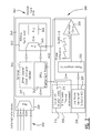
- FIG. 1 illustrates an embodiment of a system 100 for producing a system clock signal according to the invention.
- the system 100 comprises a local oscillator 110 configured to generate a first clock signal 111.
- the local oscillator is e.g. an oven controlled crystal oscillator or a temperature compensated crystal oscillator.
- the system comprises an obtaining module 120 which is configured to obtain a second clock signal 121.
- an extractor 180 to extract a third clock signal 181 from at least one external signal 122 received at the system 100.
- the second clock signal could be the same as the third clock signal, in which case the obtaining module 120 and the extractor 180 are the same module, see also the exemplary embodiments of figures 2 and 3 discussed below.
- the extractor may be configured to extract from a number of external signals 122 a quality of a clock signal included in the external signal. Using this quality, the extractor may extract the best external signal and decide to use the clock signal of this best external signal as the third clock signal 181.
- the system 100 comprises a temperature detector which is configured to detect a temperature change above a critical value in an area including the local oscillator 110.
- a temperature detector which is configured to detect a temperature change above a critical value in an area including the local oscillator 110.
- the detector 130 may be further adapted to decide to remain in the reverse hold-over mode for a minimum period of time in which period the systems needs to be stable, i.e. in which period no further significant temperature variations may be detected, before the system may switch back to the normal mode.
- the temperature detector 130 provides a detection signal to a clock generator 140 to indicate whether a temperature change above the critical value has been detected, i.e. whether to change from the normal to the reverse hold-over mode.
- the clock generator 140 is provided with the first clock signal 111 from the local oscillator 110 and with the second clock signal 121 from the extractor 120. Using this first and second clock signal, the clock generator 140 generates a system clock signal 141.
- the clock generator 140 is adapted to generate the system clock signal 141 in a first manner when no temperature change above the critical value is detected, and in a second manner when a temperature change above the critical value is detected. According to the first manner, the first clock signal 111 is used to generate the system clock 141, wherein the second clock signal 121 may be used to correct the first clock signal 111. According to the second manner, the second clock signal 121 is used to generate the system clock signal 141.
- FIG. 2 illustrates a more detailed second embodiment of a system 200 of the invention.
- the system 200 comprises a local oscillator 210, e.g. running at 10 MHz, an extractor 220 for extracting a second clock signal from an external signal, a temperature detector 230, and a clock generator 240 for generating a system clock.
- the second clock signal may e.g. be running at 100 MHz, while the system clock signal could be running at 200 MHz.
- the temperature detector 230 comprises a further local oscillator 231 having a low thermal inertia compared to the local oscillator 210.
- the output of the local oscillator 210 and of the further oscillator 231 are fed into a phase comparator 232.
- the local oscillator 210 and the further oscillator 231 are placed in the same thermal environment 250.
- the phase comparator 231 evaluates the difference in phase between the signal from the local oscillator 210 and from the further oscillator 231 in function of the time.
- the window comparator 233 can determine whether the temperature change in the thermal environment 250 is higher than a critical value. This result is communicated to the clock generator 240.
- the local oscillator 210 may be protected against temperature changes to some extent, while the further oscillator 230 may be a standard cheap crystal oscillator which is not protected against temperature changes.
- a frequency difference is constantly being monitored using the phase comparator 232, and when this frequency difference suddenly changes, this is an indication that a temperature gradient is present. The amount of the sudden frequency change is a measure of the temperature gradient and allows assessment of whether the frequency of the first clock signal will be affected by the temperature change or not.
- any other suitable oscillator may be used.
- the clock generator 240 comprises an optional processing block 244 which is configured for multiplying or dividing the frequency of the second clock signal 221 with a predetermined factor and/or for cleaning jitter in the second clock signal 221.
- a multiplier "2" will be used.
- the clock generator 240 comprises a digital PLL 242 which uses the first clock signal 211 as a master clock signal or base clock. This master clock signal is multiplied with a correction factor which is determined using the second clock signal 221 derived from the one or more external references.
- the output of the digital PLL 242 is fed into a hitless switchover block 242 which performs a hitless switchover.
- the hitless switchover block 243 uses the output of the temperature detector 230 to determine how to set a multiplexer 245.
- the output of the DPLL 242 is passed by the multiplexer 245 to a PLL 246, and the system clock will be equal to the output of the DPLL 242.
- the multiplexer switches, and allows the output of the processing block 244 to be fed in the PLL 246.
- the PLL 246 will ensure that when a switching of the multiplexer 245 takes place, the transition from the output signal of the DPLL 242 to the output of the processing block 244 en vice versa happens smoothly by adjusting the phase.
- the hitless switchover block 242 may be further provided with a button to perform a manual switchover of the multiplexer 245. In that way, when a critical temperature change is expected, e.g. because of maintenance operations to the cabinet, it can be decided to use the second clock signal 221 from the external references instead of the first clock signal 211 from the local oscillator 210.
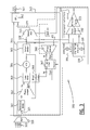
- FIG 3 illustrates a third embodiment of a system 300 of the invention.
- the system 300 comprises a local oscillator 310, an extractor 320, a temperature detector 330, and a clock generator 340.
- the temperature detector 330 is identical to the temperature detector 230 described above with reference to figure 2 , and hence a detailed description thereof has been omitted.
- the temperature detector 330 comprises an oscillator 331 having a low thermal inertia compared to the local oscillator 310, a phase comparator 332, and a window comparator 333.
- the clock generator 340 comprises a multiplexer 345 which will allow the first clock signal 311 of the local oscillator 310 to pass as the master clock signal 371 to the input of a digital PLL 342, when no critical temperature change has been detected by the temperature detector 330.
- the clock generator 340 further comprises a processing block 344 which is adapted to ensure that the second clock signal 321 derived from one or more external reference signals 322 is in phase with the first clock signal 311. Further, the processing block 344 may be adapted to multiply or divide the second clock signal 321 with a suitable factor. This processed second clock signal is fed into the multiplexor 345, and will be selected by the multiplexor 345 when the detected temperature change is above a critical value.
- the settings of the feedback loop of processing block 344 will be frozen, see further, so that the first clock signal no longer influences the processed second clock signal.
- the master clock signal that is fed in the DPLL 342 will be either the first clock signal 311 or the processed second clock signal 321' depending on whether a critical temperature change has been detected.
- the multiplexor may switch back to the first clock signal.
- a delay may be introduced, see block 369, so that the switching is done when there is no phase difference between the first clock signal 311 and the processed second clock signal 321', which will be detected by the phase comparator 368.
- the DPLL 342 corrects the master clock signal 371, being either the first clock signal 311 or the processed second clock signal 321' depending on whether a critical temperature change has been detected, with a correction factor which is determined using the second clock signal 321 derived from the one or more external references 322.
- the processing block 344 comprises a reference divider 361, a phase comparator 362, a loop filter 363 having a high bandwidth, a VCO 364, an output divider 365 and a feedback divider 366.
- the reference divider 361 and the output divider 365 are typically configured at fixed values.
- the feedback divider 366 is configured with a value which is dependent on the phase difference between the first clock signal 311 and the output 321' of the PLL 344, using phase comparator 368 and averaging filter 367. In that way the PLL's output 321' can be brought to be in phase with the first clock signal 311. This will allow a so-called hitless switch-over in a temperature gradient is detected. Further, when a temperature gradient is detected, the parameters of the averaging filter 367 are frozen until the temperature is again stable.
- the first clock signal 311 from the local oscillator 310 is replaced with a clock 321' of the same frequency and phase, but derived directly from the selected external reference clock, through a VCO 364 with high bandwidth.
- the oscillator in this VCO 364 will also be suffering from the temperature effects that invalidate the local oscillator 310 as local reference, but the impact of this on the VCO output will be neutralized by virtue of the high bandwidth commodity of the loop filter 363, which will make it track accurately the stable external reference clock 321, despite changes in the control voltage to frequency characteristic of the VCO 364.
- This third embodiment may provide an even better system clock behavior, as the system clock remains generated by the DPLL 342 in both situations, only using a different input base clock 371 for each situation.
- processing block 344 is actually a DPLL which uses the second clock signal 321 as a master clock to produce the processed second signal 321' which is in frequency and phase identical to the first clock signal 311 produced by the local oscillator 310 for as long as no harmful temperature gradient was detected. Therefore processing block 344 may be replaced by any other known DPLL with the similar functionality.
- this divider/multiplier may be a divide/multiply with "1”, and that a divider may be a multiplier and vice versa.
- extractor and clock generator modules may be implemented using hardware and/or software components as will be apparent to the skilled person.
- Timing dependent systems containing conventional temperature sensors and switches have the following disadvantage compared to embodiments of the present invention.
- Such sensors and switches are intended for regulating its cooling, and for protection (preventive power down) of the equipment against overheating.
- These sensors are of little use for detecting the kind of temperature variations that may impair the internal timing logic of such systems in time, and hence for protecting against such variations.
- the temperature gradient detection of preferred embodiments of the invention only requires one low cost crystal oscillator and a very small additional silicon area for implementing the phase comparator and window comparator, and can report temperature gradients before they affect the local oscillator.
Landscapes
- Physics & Mathematics (AREA)
- General Physics & Mathematics (AREA)
- Stabilization Of Oscillater, Synchronisation, Frequency Synthesizers (AREA)
Priority Applications (6)
| Application Number | Priority Date | Filing Date | Title |
|---|---|---|---|
| EP12306012.1A EP2701309A1 (fr) | 2012-08-21 | 2012-08-21 | Système pour produire une horloge de système et système de détection de gradient de température |
| US14/416,467 US9537446B2 (en) | 2012-08-21 | 2013-08-19 | System for producing a system clock and temperature gradient detection system |
| JP2015527876A JP6133986B2 (ja) | 2012-08-21 | 2013-08-19 | システム・クロックを発生させるためのシステム、および温度勾配検出システム |
| CN201380043676.2A CN104584436A (zh) | 2012-08-21 | 2013-08-19 | 用于产生系统时钟的系统及温度梯度检测系统 |
| PCT/EP2013/067212 WO2014029718A1 (fr) | 2012-08-21 | 2013-08-19 | Système pour fabriquer une horloge de système et système de détection de gradient de température |
| KR1020157006966A KR20150045490A (ko) | 2012-08-21 | 2013-08-19 | 시스템 클럭을 생성하기 위한 시스템 및 온도 구배 검출 시스템 |
Applications Claiming Priority (1)
| Application Number | Priority Date | Filing Date | Title |
|---|---|---|---|
| EP12306012.1A EP2701309A1 (fr) | 2012-08-21 | 2012-08-21 | Système pour produire une horloge de système et système de détection de gradient de température |
Publications (1)
| Publication Number | Publication Date |
|---|---|
| EP2701309A1 true EP2701309A1 (fr) | 2014-02-26 |
Family
ID=46796493
Family Applications (1)
| Application Number | Title | Priority Date | Filing Date |
|---|---|---|---|
| EP12306012.1A Withdrawn EP2701309A1 (fr) | 2012-08-21 | 2012-08-21 | Système pour produire une horloge de système et système de détection de gradient de température |
Country Status (6)
| Country | Link |
|---|---|
| US (1) | US9537446B2 (fr) |
| EP (1) | EP2701309A1 (fr) |
| JP (1) | JP6133986B2 (fr) |
| KR (1) | KR20150045490A (fr) |
| CN (1) | CN104584436A (fr) |
| WO (1) | WO2014029718A1 (fr) |
Cited By (2)
| Publication number | Priority date | Publication date | Assignee | Title |
|---|---|---|---|---|
| US9608751B2 (en) | 2015-03-18 | 2017-03-28 | Accedian Networks Inc. | Simplified synchronized Ethernet implementation |
| EP3667929A3 (fr) * | 2018-11-23 | 2020-10-28 | FRAUNHOFER-GESELLSCHAFT zur Förderung der angewandten Forschung e.V. | Neutralisation des influences de l'environnement sur les parametres d'emission |
Families Citing this family (5)
| Publication number | Priority date | Publication date | Assignee | Title |
|---|---|---|---|---|
| US10318370B2 (en) * | 2016-03-25 | 2019-06-11 | Seiko Epson Corporation | Circuit device, physical quantity detection device, oscillator, electronic apparatus, vehicle, and method of detecting failure of master clock signal |
| US9991898B1 (en) * | 2016-11-16 | 2018-06-05 | Perceptia Devices, Inc. | Fractional-N jitter attenuator |
| CN109217821B (zh) * | 2017-07-03 | 2024-02-09 | 中兴通讯股份有限公司 | 频率器件补偿方法、装置、系统及计算机可读存储介质 |
| US11152947B2 (en) | 2019-02-20 | 2021-10-19 | Renesas Electronics America Inc. | Feedback control for accurate signal generation |
| CN117111434B (zh) * | 2023-08-17 | 2024-03-29 | 湖南时空信安科技有限公司 | 一种时钟性能的评估方法、装置及终端设备 |
Citations (4)
| Publication number | Priority date | Publication date | Assignee | Title |
|---|---|---|---|---|
| US6711230B1 (en) * | 2002-09-27 | 2004-03-23 | Nortel Networks Limited | Reference timing signal oscillator with frequency stability |
| US20070182467A1 (en) * | 2006-02-08 | 2007-08-09 | Fujitsu Limited | DPLL circuit having holdover function |
| US7764133B1 (en) * | 2007-07-12 | 2010-07-27 | Nortel Networks Limited | Time based predictive algorithm system for a crystal oscillator |
| WO2011086976A1 (fr) * | 2010-01-13 | 2011-07-21 | 古野電気株式会社 | Dispositif générateur de fréquence de référence |
Family Cites Families (8)
| Publication number | Priority date | Publication date | Assignee | Title |
|---|---|---|---|---|
| JPS60125021A (ja) * | 1983-12-12 | 1985-07-04 | Matsushita Electric Ind Co Ltd | 位相制御ル−プの疑似同期検出装置 |
| JPS63311133A (ja) * | 1987-06-12 | 1988-12-19 | Sumitomo Metal Ind Ltd | 水晶温度センサ |
| JPH03251912A (ja) * | 1990-03-01 | 1991-11-11 | Toshiba Corp | システムクロック切替え機能を持つ電子機器 |
| JPH0468903A (ja) * | 1990-07-07 | 1992-03-04 | Asahi Denpa Kk | 温度検知機能を有する発振器および水晶発振素子並びに温度検出方法 |
| US7167993B1 (en) * | 1994-06-20 | 2007-01-23 | Thomas C Douglass | Thermal and power management for computer systems |
| JP4644822B2 (ja) * | 2007-01-17 | 2011-03-09 | 日本電信電話株式会社 | 自動周波数制御回路 |
| US8525840B2 (en) * | 2008-05-15 | 2013-09-03 | Apple Inc. | Thermal management of graphics processing units |
| JP2012060583A (ja) * | 2010-09-13 | 2012-03-22 | Kyocera Corp | クロック発生装置 |
-
2012
- 2012-08-21 EP EP12306012.1A patent/EP2701309A1/fr not_active Withdrawn
-
2013
- 2013-08-19 KR KR1020157006966A patent/KR20150045490A/ko not_active Application Discontinuation
- 2013-08-19 CN CN201380043676.2A patent/CN104584436A/zh active Pending
- 2013-08-19 US US14/416,467 patent/US9537446B2/en active Active
- 2013-08-19 JP JP2015527876A patent/JP6133986B2/ja not_active Expired - Fee Related
- 2013-08-19 WO PCT/EP2013/067212 patent/WO2014029718A1/fr active Application Filing
Patent Citations (5)
| Publication number | Priority date | Publication date | Assignee | Title |
|---|---|---|---|---|
| US6711230B1 (en) * | 2002-09-27 | 2004-03-23 | Nortel Networks Limited | Reference timing signal oscillator with frequency stability |
| US20070182467A1 (en) * | 2006-02-08 | 2007-08-09 | Fujitsu Limited | DPLL circuit having holdover function |
| US7764133B1 (en) * | 2007-07-12 | 2010-07-27 | Nortel Networks Limited | Time based predictive algorithm system for a crystal oscillator |
| WO2011086976A1 (fr) * | 2010-01-13 | 2011-07-21 | 古野電気株式会社 | Dispositif générateur de fréquence de référence |
| EP2525494A1 (fr) * | 2010-01-13 | 2012-11-21 | Furuno Electric Co., Ltd. | Dispositif générateur de fréquence de référence |
Cited By (4)
| Publication number | Priority date | Publication date | Assignee | Title |
|---|---|---|---|---|
| US9608751B2 (en) | 2015-03-18 | 2017-03-28 | Accedian Networks Inc. | Simplified synchronized Ethernet implementation |
| US9887794B2 (en) | 2015-03-18 | 2018-02-06 | Accedian Networks Inc. | Simplified synchronized Ethernet implementation |
| US10419144B2 (en) | 2015-03-18 | 2019-09-17 | Accedian Networks Inc. | Simplified synchronized ethernet implementation |
| EP3667929A3 (fr) * | 2018-11-23 | 2020-10-28 | FRAUNHOFER-GESELLSCHAFT zur Förderung der angewandten Forschung e.V. | Neutralisation des influences de l'environnement sur les parametres d'emission |
Also Published As
| Publication number | Publication date |
|---|---|
| JP2015527013A (ja) | 2015-09-10 |
| WO2014029718A1 (fr) | 2014-02-27 |
| US9537446B2 (en) | 2017-01-03 |
| JP6133986B2 (ja) | 2017-05-24 |
| US20150180409A1 (en) | 2015-06-25 |
| KR20150045490A (ko) | 2015-04-28 |
| CN104584436A (zh) | 2015-04-29 |
Similar Documents
| Publication | Publication Date | Title |
|---|---|---|
| US9537446B2 (en) | System for producing a system clock and temperature gradient detection system | |
| JP6664438B2 (ja) | クロック同期および周波数変換のための装置および方法 | |
| EP2528255B1 (fr) | Procédé et dispositif à reglage de fréquence | |
| US10608647B1 (en) | Delay adjustment using frequency estimation | |
| US20170214516A1 (en) | System and method for managing holdover | |
| JP4051840B2 (ja) | 分散されているシステム機器の同期装置 | |
| US10908635B1 (en) | Detection and management of frequency errors in a reference input clock signal | |
| US10483987B1 (en) | Failsafe clock product using frequency estimation | |
| US20110234277A1 (en) | Apparatus and method to compensate for injection locking | |
| KR101795199B1 (ko) | 신호 처리 장치 | |
| EP2509251B1 (fr) | Procédé et dispositif de contrôle de synchronisation de fréquence | |
| US7701268B2 (en) | Clock generation circuit | |
| CN101026377A (zh) | 时钟产生电路 | |
| JP4535288B2 (ja) | 分散制御システム | |
| US20210302499A1 (en) | Clock frequency monitoring device and clock frequency monitoring method | |
| US20230216653A1 (en) | Data transfer circuit and communication apparatus | |
| CA3080598C (fr) | Procede pour limiter une suroscillation de la frequence dans une boucle de delai de recuperation | |
| JP5035383B2 (ja) | 分散制御システム | |
| Chowdhury | Timing Parameters | |
| JP6780493B2 (ja) | 従属同期回路 | |
| JP2011182099A (ja) | 基準信号発生装置及び方法 | |
| US8330497B1 (en) | Frequency monitoring systems and methods | |
| KR100333258B1 (ko) | 이중화 시간/주파수 발생장치의 주파수 제어방법 | |
| WO2011079430A1 (fr) | Système et procédé de réglage de fréquence d'horloge | |
| JP2003338810A (ja) | 網クロックの周波数安定度判定方法およびその回路 |
Legal Events
| Date | Code | Title | Description |
|---|---|---|---|
| PUAI | Public reference made under article 153(3) epc to a published international application that has entered the european phase |
Free format text: ORIGINAL CODE: 0009012 |
|
| AK | Designated contracting states |
Kind code of ref document: A1 Designated state(s): AL AT BE BG CH CY CZ DE DK EE ES FI FR GB GR HR HU IE IS IT LI LT LU LV MC MK MT NL NO PL PT RO RS SE SI SK SM TR |
|
| AX | Request for extension of the european patent |
Extension state: BA ME |
|
| 111Z | Information provided on other rights and legal means of execution |
Free format text: AL AT BE BG CH CY CZ DE DK EE ES FI FR GB GR HR HU IE IS IT LI LT LU LV MC MK MT NL NO PL PT RO RS SE SI SK SM TR Effective date: 20140516 |
|
| RAP1 | Party data changed (applicant data changed or rights of an application transferred) |
Owner name: ALCATEL LUCENT |
|
| 17P | Request for examination filed |
Effective date: 20140826 |
|
| RBV | Designated contracting states (corrected) |
Designated state(s): AL AT BE BG CH CY CZ DE DK EE ES FI FR GB GR HR HU IE IS IT LI LT LU LV MC MK MT NL NO PL PT RO RS SE SI SK SM TR |
|
| D11X | Information provided on other rights and legal means of execution (deleted) | ||
| 17Q | First examination report despatched |
Effective date: 20170928 |
|
| RAP1 | Party data changed (applicant data changed or rights of an application transferred) |
Owner name: ALCATEL LUCENT |
|
| STAA | Information on the status of an ep patent application or granted ep patent |
Free format text: STATUS: THE APPLICATION IS DEEMED TO BE WITHDRAWN |
|
| 18D | Application deemed to be withdrawn |
Effective date: 20180410 |