EP2696379A2 - Light emitting device - Google Patents
Light emitting device Download PDFInfo
- Publication number
- EP2696379A2 EP2696379A2 EP13177955.5A EP13177955A EP2696379A2 EP 2696379 A2 EP2696379 A2 EP 2696379A2 EP 13177955 A EP13177955 A EP 13177955A EP 2696379 A2 EP2696379 A2 EP 2696379A2
- Authority
- EP
- European Patent Office
- Prior art keywords
- light emitting
- hole
- emitting device
- disposed
- substrate
- Prior art date
- Legal status (The legal status is an assumption and is not a legal conclusion. Google has not performed a legal analysis and makes no representation as to the accuracy of the status listed.)
- Granted
Links
Images


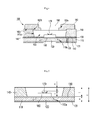


Classifications
-
- H—ELECTRICITY
- H10—SEMICONDUCTOR DEVICES; ELECTRIC SOLID-STATE DEVICES NOT OTHERWISE PROVIDED FOR
- H10H—INORGANIC LIGHT-EMITTING SEMICONDUCTOR DEVICES HAVING POTENTIAL BARRIERS
- H10H20/00—Individual inorganic light-emitting semiconductor devices having potential barriers, e.g. light-emitting diodes [LED]
- H10H20/80—Constructional details
- H10H20/85—Packages
-
- H—ELECTRICITY
- H10—SEMICONDUCTOR DEVICES; ELECTRIC SOLID-STATE DEVICES NOT OTHERWISE PROVIDED FOR
- H10H—INORGANIC LIGHT-EMITTING SEMICONDUCTOR DEVICES HAVING POTENTIAL BARRIERS
- H10H20/00—Individual inorganic light-emitting semiconductor devices having potential barriers, e.g. light-emitting diodes [LED]
- H10H20/80—Constructional details
- H10H20/85—Packages
- H10H20/858—Means for heat extraction or cooling
- H10H20/8582—Means for heat extraction or cooling characterised by their shape
-
- F—MECHANICAL ENGINEERING; LIGHTING; HEATING; WEAPONS; BLASTING
- F21—LIGHTING
- F21V—FUNCTIONAL FEATURES OR DETAILS OF LIGHTING DEVICES OR SYSTEMS THEREOF; STRUCTURAL COMBINATIONS OF LIGHTING DEVICES WITH OTHER ARTICLES, NOT OTHERWISE PROVIDED FOR
- F21V29/00—Protecting lighting devices from thermal damage; Cooling or heating arrangements specially adapted for lighting devices or systems
- F21V29/50—Cooling arrangements
- F21V29/502—Cooling arrangements characterised by the adaptation for cooling of specific components
- F21V29/503—Cooling arrangements characterised by the adaptation for cooling of specific components of light sources
-
- F—MECHANICAL ENGINEERING; LIGHTING; HEATING; WEAPONS; BLASTING
- F21—LIGHTING
- F21V—FUNCTIONAL FEATURES OR DETAILS OF LIGHTING DEVICES OR SYSTEMS THEREOF; STRUCTURAL COMBINATIONS OF LIGHTING DEVICES WITH OTHER ARTICLES, NOT OTHERWISE PROVIDED FOR
- F21V19/00—Fastening of light sources or lamp holders
- F21V19/001—Fastening of light sources or lamp holders the light sources being semiconductors devices, e.g. LEDs
-
- F—MECHANICAL ENGINEERING; LIGHTING; HEATING; WEAPONS; BLASTING
- F21—LIGHTING
- F21V—FUNCTIONAL FEATURES OR DETAILS OF LIGHTING DEVICES OR SYSTEMS THEREOF; STRUCTURAL COMBINATIONS OF LIGHTING DEVICES WITH OTHER ARTICLES, NOT OTHERWISE PROVIDED FOR
- F21V29/00—Protecting lighting devices from thermal damage; Cooling or heating arrangements specially adapted for lighting devices or systems
- F21V29/50—Cooling arrangements
- F21V29/70—Cooling arrangements characterised by passive heat-dissipating elements, e.g. heat-sinks
-
- F—MECHANICAL ENGINEERING; LIGHTING; HEATING; WEAPONS; BLASTING
- F21—LIGHTING
- F21V—FUNCTIONAL FEATURES OR DETAILS OF LIGHTING DEVICES OR SYSTEMS THEREOF; STRUCTURAL COMBINATIONS OF LIGHTING DEVICES WITH OTHER ARTICLES, NOT OTHERWISE PROVIDED FOR
- F21V29/00—Protecting lighting devices from thermal damage; Cooling or heating arrangements specially adapted for lighting devices or systems
- F21V29/50—Cooling arrangements
- F21V29/70—Cooling arrangements characterised by passive heat-dissipating elements, e.g. heat-sinks
- F21V29/83—Cooling arrangements characterised by passive heat-dissipating elements, e.g. heat-sinks the elements having apertures, ducts or channels, e.g. heat radiation holes
-
- H—ELECTRICITY
- H10—SEMICONDUCTOR DEVICES; ELECTRIC SOLID-STATE DEVICES NOT OTHERWISE PROVIDED FOR
- H10H—INORGANIC LIGHT-EMITTING SEMICONDUCTOR DEVICES HAVING POTENTIAL BARRIERS
- H10H20/00—Individual inorganic light-emitting semiconductor devices having potential barriers, e.g. light-emitting diodes [LED]
- H10H20/80—Constructional details
- H10H20/85—Packages
- H10H20/855—Optical field-shaping means, e.g. lenses
-
- H—ELECTRICITY
- H10—SEMICONDUCTOR DEVICES; ELECTRIC SOLID-STATE DEVICES NOT OTHERWISE PROVIDED FOR
- H10H—INORGANIC LIGHT-EMITTING SEMICONDUCTOR DEVICES HAVING POTENTIAL BARRIERS
- H10H20/00—Individual inorganic light-emitting semiconductor devices having potential barriers, e.g. light-emitting diodes [LED]
- H10H20/80—Constructional details
- H10H20/85—Packages
- H10H20/8506—Containers
Definitions
- This embodiment relates to a light emitting device.
- a light emitting device including a laser diode or a light emitting diode formed by using group III to V or group II to VI compound semiconductor materials of a semiconductor is able to create a variety of colors, for example, red, green, blue lights, an ultraviolet ray and the like.
- the light emitting device is also able to create high efficient white light by use of a fluorescent material or by a combination of the colors.
- the light emitting device has low power consumption, a semi-permanent span of life, a rapid response speed, safeness and an environment-friendliness
- the light emitting device or the light emitting diode is being increasingly applied to a transmission module of an optical communication means, a light emitting diode backlight replacing a cold cathode fluorescence lamp (CCFL) constituting the backlight of a liquid crystal display (LCD), a white light emitting diode lighting device replacing the fluorescent lamp or the incandescent bulb, a headlight of an automobile and a traffic light.
- a light emitting diode backlight replacing a cold cathode fluorescence lamp (CCFL) constituting the backlight of a liquid crystal display (LCD)
- CCFL cold cathode fluorescence lamp
- LCD liquid crystal display
- white light emitting diode lighting device replacing the fluorescent lamp or the incandescent bulb
- a headlight of an automobile a traffic light.
- a light emitting package including a UV LED mounted on a metal substrate
- ultraviolet reflected light reaches an insulation layer on the metal substrate, and thus, an organic material included in the insulation layer is discolored or deteriorated. As a result, light output of the light emitting device is degraded and reliability is reduced.
- the lighting device includes: a substrate; a body which is disposed on the substrate and has a first hole having a predetermined size; a light emitting chip which is disposed within a cavity formed by the substrate and the first hole of the body; a cap which is disposed on the body and has a second hole having a predetermined size; and a transparent window which is disposed in the second hole.
- a thickness or a size of each layer may be magnified, omitted or schematically shown for the purpose of convenience and clearness of description.
- the size of each component may not necessarily mean its actual size.
- Figs. 1 to 7 are views of a light emitting device according to a first embodiment.
- Fig. 1 is a perspective view of the light emitting device according to the first embodiment.
- Fig. 2 is an exploded perspective view of the light emitting device shown in Fig. 1 .
- Fig. 3 is an exploded view formed by cutting the light emitting device shown in Fig. 1 along line A-A'.
- Fig. 4 is a cross sectional view formed by cutting the light emitting device shown in Fig. 1 along line A-A'.
- Figs. 5 to 7 are cross sectional views showing design measures of the light emitting device.
- a light emitting device 100 includes, as shown in Figs. 1 to 4 , a substrate 110, a body 140 which is disposed on the substrate 110 and has a through-hole 140a formed therein, at least one light emitting chip 170 which is disposed within a cavity 150 formed by the substrate 110 and the through-hole 140a, a cap 180 which is disposed on the body 140 and has a through-hole 180a formed therein, and a transparent window 190 which is disposed within the through-hole 180a of the cap 180.
- the substrate 110 may also include a through-hole 110a and a heat radiation block 120 disposed within the through-hole 110a.
- the substrate 110 may be divided into a ceramic-made body and the heat radiation block 120 inserted into the through-hole 110a.
- the light emitting chip 170 may be more attached and fixed to a sub-mount 160, and disposed on the substrate 110.
- the sub-mount 160 may be disposed on the heat radiation block 120.
- the through-hole 140a, the through-hole 180a and the through-hole 110a may be designated as a first hole, a second hole and a third hole respectively in order that they are distinguished from each other.
- the substrate 110 may be a single-layered substrate or a multi-layered ceramic substrate.
- the substrate 110 can be formed by using a high temperature co-fired ceramic (HTCC) technology.
- HTCC high temperature co-fired ceramic
- the high temperature co-fired ceramic may be formed by co-firing ceramic sheets at a high temperature higher than 1,200 °C
- the substrate 110 may be composed of, for example, the high temperature co-fired ceramic (HTCC) or a low temperature co-fired ceramic (LTCC).
- HTCC high temperature co-fired ceramic
- LTCC low temperature co-fired ceramic
- the thicknesses of the layers of the multi-layered ceramic substrate may be the same as each other or may be different from each other. There is no limit to the thickness.
- the substrate 110 includes a ceramic substrate, hereafter, the substrate 110 is denoted by a ceramic substrate.
- the ceramic substrate 110 has a thermal conductivity less than that of a metallic material. Therefore, for the purpose of compensating for thermal characteristics, the metal slug-made heat radiation block 120 is co-fired or is heat-treated in an AgCu bonding process, and then is coupled to or inserted into the ceramic substrate 110.
- a zener-diode may be mounted on a position of the ceramic substrate 110 or the body 140, which is separated from the space where the light emitting chip 170 is located.
- the through-hole 110a of the ceramic substrate 110 is stepped, so that a contact area with the heat radiation block 120 is increased, and thus, heat radiation effect is improved.
- the ceramic substrate 110 may be formed of a nitride insulating material or an oxide insulating material.
- the ceramic substrate 110 may include SiO 2 , Si x O y , Si 3 N y , SiO x N y , Al 2 O 3 , or AlN.
- the ceramic substrate 110 may not include the heat radiation block 120.
- Conductive patterns 142 and 143 may be disposed on the upper surface of the ceramic substrate 110. And conductive patterns may be disposed on the lower surface of the ceramic substrate 110.
- the ceramic substrate 110 may have a via hole 132 disposed on one side thereof.
- the conductive patterns disposed on the upper surface and lower surface of the ceramic substrate 110 may be electrically connected to each other through the via hole 132.
- the via hole 132 is not shown in the following drawings, the via hole 132 is not nonexistent.
- the via hole 132 may or may not be represented in the direction of the section.
- the heat radiation block 120 functions to radiate heat generated from the light emitting chip 170. Therefore, the heat radiation block 120 may include metals having excellent thermal conductivity. For instance, the heat radiation block 120 may include at least one of Mo, W, Au, Ag, a Cu single metal and an alloy including Cu, for example, CuW and CuMo.
- the heat generated from the light emitting chip 170 is radiated outwardly through the heat radiation block 120 having excellent thermal conductivity, so that the thermal characteristics and the reliability of the light emitting device 100 may be improved.
- the heat radiation block 120 is co-fired or is heat-treated in an AgCu bonding process, and then is coupled to or inserted into the through-hole 110a of the ceramic substrate 110.
- the heat radiation block 120 including CuW is inserted into the substrate 110, so that the ceramic substrate 110 may be stable to the heat.
- the heat radiation block 120 including Ag is inserted into the substrate 110, so that the ceramic substrate 110 may become thermally resistant.
- the constituent materials of the ceramic substrate 110 and the heat radiation block 120 are different from each other, and thus, the thermal expansion coefficients of the ceramic substrate 110 and the heat radiation block 120 are also different from each other. Therefore, the heat radiation block 120 is inserted into the ceramic substrate 110, and then is co-fired, or the heat radiation block 120 is expanded by the heat generated from the light emitting chip 170 during the use of the light emitting device. As a result, the top surface of the heat radiation block 120 on which the light emitting chip 170 is mounted may convexly project.
- a first projection prevention layer 130 is located between the light emitting chip 170 and the heat radiation block 120, thereby preventing the top surface of the heat radiation block 120 from projecting toward the light emitting chip 170.
- the first projection prevention layer 130 may be disposed on the ceramic substrate 110 and on the heat radiation block 120 or may form a portion of the ceramic substrate 110 by being integrally formed with the ceramic substrate 110.
- a second projection prevention layer 131 may be disposed under the ceramic substrate 110 and the heat radiation block 120 because the bottom surface of the heat radiation block 120 as well as the top surface of the heat radiation block 120 may convexly project.
- the body 140 having the cavity 150 formed therein is disposed on the first projection prevention layer 130.
- the inner side wall of the body 140 may be inclined or not.
- the inner side wall of the body 140 may be formed in the form of stairs or may be vertically formed.
- the inclined side wall of the body 140 causes the light generated from the light emitting chip 170 to be reflected from the side wall formed by the through-hole 140a and to travel toward the open cavity 150.
- light-extraction efficiency of the light emitting device 100 can be enhanced.
- the through-hole 140a which is formed in the form of stairs or is formed vertically can be mechanically implemented by a drilling process or can be implemented by stacking and firing a plurality of ceramic layers having mutually different lengths when the body 140 is comprised of a multi-layer ceramic substrate.
- the method for implementing the through-hole 140 is not limited to this.
- a reflective layer may be coated on at least a portion of the side wall formed by the through-hole 140a of the body 140 and/or on at least a portion of the bottom surface of the body 140.
- the ceramic material constituting the body 140 allows the cavity 150 to be easily formed in the process and is resistant to the heat.
- the sub-mount 160 When the sub-mount 160 is disposed on the first projection prevention layer 130, it is possible more effectively to prevent the heat radiation block 120 from becoming convex than to prevent the heat radiation block 120 from becoming convex only by using the first projection prevention layer 130.
- the sub-mount 160 may be a conductive substrate or an insulating substrate.
- the sub-mount 160 may include materials such as Si, SiC, AlN or the like, considering thermal conductivity and thermal expansion coefficient.
- a conductive pattern (not shown) may be formed on the sub-mount 160.
- the light emitting chip 170 may be electrically connected to the conductive pattern.
- the light emitting chip 170 can be fixed through Au paste boding or Au-Sn eutectic boding.
- the bonding may be performed by heating the Au paste at a temperature lower than 280 °C in order to prevent the light emitting chip 170 from being damaged by the heat.
- the sub-mount 160 may be formed of a material having excellent thermal conductivity.
- the sub-mount 160 is disposed on the heat radiation block 120, the heat generated from the light emitting chip 170 is radiated outwardly through the heat radiation block 120 having excellent thermal conductivity instead of the ceramic substrate 110 having relatively less thermal conductivity than that of the heat radiation block 120. As a result, the reliability of the light emitting device 100 can be improved.
- the light emitting chip 170 is directly mounted on the heat radiation block 120, when the top surface of the heat radiation block 120, on which the light emitting chip 170 is mounted, is not flat, the light emitting chip 170 comes off the heat radiation block 120 or is unstably bonded, so that heat radiation performance may be degraded. This problem can be minimized by disposing the light emitting chip 170 on the sub-mount 160 or directly on the first projection prevention layer 130 without the sub-mount 160.
- the heat radiation block 120 functions to radiate outwardly the heat generated from the light emitting chip 170 and maintain the reliability of the light emitting device 100. Therefore, the heat radiation block 120 and the light emitting chip 170 may be disposed perpendicular to and overlapped with each other.
- the light emitting chip 170 includes a light emitting diode (LED) formed by using a plurality of compound semiconductor layers, for example, a group III to V semiconductor layer.
- the LED may be a colored LED emitting blue, green or red light, etc., or may be a UV LED.
- the light emitted from the LED can be created by using a variety of semiconductors. The method for creating the light emitted from the LED is not limited to this.
- the ceramic substrate 110 and the body 140 are composed of an inorganic ceramic. Therefore, even when a light emitting chip including a deep UV LED having a wavelength of about 200 nm to 300 nm or a near UV LED having a wavelength of about 300nm to 400nm is used, it is not expected that the upper body and lower body are discolored or deteriorated by UV light emitted from the light emitting chip. Accordingly, reliability of the light emitting device can be maintained.
- the light emitting chip 170 may be bonded in a flip-chip manner or may be fixed on the ceramic substrate 110 by Au paste using bonding or by Au-Sn eutectic bonding.
- the bonding may be performed by heating the Au paste at a temperature lower than 280 °C.
- the cap 180 having the through-hole 180a in which the transparent window 190 has been disposed may be disposed on the body 140.
- the through-hole 180a of the cap 180 may have a level difference surface.
- an upper diameter of the through-hole 180a may be formed to be larger than a lower diameter of the through-hole 180a.
- a level difference is formed on an outer circumferential surface of the transparent window 190 in such a manner as to face the level difference surface of the through-hole 180a and is disposed within the through-hole 180a of the cap 180.
- the through-hole 180a may have a circular shape.
- the shape of the through-hole 180a is not limited to the circular shape.
- the through-hole 180a may have a quadrangular shape. More specifically, the through-hole 180a may have a square shape or a rectangular shape. Also, the through-hole 180a may have a polygonal shape as well as the circular and quadrangular shapes.
- the transparent window 190 may have a shape corresponding to the various shapes of the through-hole 180a.
- a level difference surface 180b may be formed on the lower portion of the cap 180.
- the lower portion of the cap is divided into a first surface and a second surface more projecting downwardly than the first surface. At least a portion of the first surface may be attached and fixed to the body. Through this, when the cap 180 is coupled to a top surface 140b of the body 140, a portion of the lower portion having the level difference surface 180b is inserted within the cavity 150.
- the cap 180 and the body 140 may be coupled to each other by a sealing process through Au-Sn eutectic boding in vacuum or nitrogen N 2 gas.
- the eutectic bonding is performed by heating an adhesive material like AuSn at a temperature higher than 280 °C. Since a ceramic material has brittleness and tends to be broken by pressure, the cap 180 and the body 140 can be attached and fixed to each other by using the eutectic bonding instead of welding.
- the cap 180 having the aforesaid configuration may be formed by using one of metallic materials including Kovar.
- the transparent window 190 may be made of a transparent material and a non-reflective coating film in order to transmit light generated from the light emitting chip 170 to the outside without absorbing the light.
- the transparent window 190 may be made of any one of SiO 2 (Quartz, UV Fused Silica), Al 2 O 3 (Sapphire), LiF, MgF 2 , CaF 2 , low iron transparent glass and glass including B 2 O 3 .
- the transparent window 190 functions to prevent ultraviolet ray emitted from the light emitting chip 170 from destroying or deteriorating external organic matters of the light emitting device 100.
- a side of the transparent window 190 which contacts with the level difference surface 180b, has a shape corresponding to the shape of the level difference surface 180b.
- a space between the transparent window 190 and the cavity 150 may be in a vacuum state or be filled with N 2 gas or forming gas.
- a thermal pad (not shown) may be disposed under the ceramic substrate 110 and the lower portion of the heat radiation block 120.
- the thermal pad may have an excellent thermal conductivity.
- the thermal pad may be comprised of a metallic material including any one of Ag, Au and Cu.
- a thermal sheet (not shown) may be disposed between the thermal pad and the ceramic substrate 110, and between the thermal pad and the heat radiation block 120.
- the thermal sheet has excellent thermal conductivity, electrical insulation and flame resistance and causes the heat generating portion and the thermal pad to contact with each other, thereby maximizing a heat transfer effect.
- the light emitting device 100 may further include a molding part (not shown) which is formed within the cavity 150 in such a manner as to surround the light emitting chip 170.
- the molding part may include at least one of Si resin which has a high or low refractive index and is mixed with a fluorescent material and hybrid resin.
- the ceramic substrate 110 and the inner side wall of the body 140 are shown in one unit respectively, there is no limit to this and each of them may be formed by stacking a plurality of layers.
- the surfaces of the through-hole 110a and 140a may be not smooth but uneven.
- Figs. 5 to 7 are cross sectional views showing design measures of the light emitting device.
- a sum "a" of a height of the ceramic substrate 110 and heights the first and the second projection prevention layers 130 and 131 may be from 0.2 mm to 0.6 mm, and more preferably 0.4 mm.
- a height "b" of the body 140 may be from 0.4 mm to 1.0 mm, and more preferably 0.7 mm.
- a sum "c" of the height of the body 140 and the height of the ceramic substrate 110 including the first and the second projection prevention layers 130 and 131 may be designed to be from 0.6 mm to 1.6 mm, and more preferably 1.1 mm.
- a sum "d" of a height of the sub-mount 160 and a height of the light emitting chip 170 may be from 0.2 mm to 0.6 mm, and more preferably 0.4 mm.
- a height "e" between the light emitting chip 170 and the top surface of the body 140 may be designed to be from 0.1 mm to 0.5 mm, and more preferably 0.3 mm.
- a thickness "t1" of the sub-mount 160 may be from 0.05 mm to 0.45 mm, and more preferably 0.25 mm.
- a gap “f" between the light emitting chip 170 and the transparent window 190 may be from 0.1 mm to 0.3 mm, and more preferably 0.2 mm.
- An upper diameter "g” of the transparent window 190 may be from 1.7 mm to 2.0 mm, and more preferably 1.9 mm.
- a lower diameter "h” of the transparent window 190 may be from 1.3 mm to 1.7 mm, and more preferably 1.5 mm.
- a thickness "t2" of the transparent window 190 may be from 0.3 mm to 0.5 mm, and more preferably 0.4 mm.
- a height "i" from the bottom surface of the cap 180 to the level difference surface may be from 0.1 mm to 0.3 mm, and more preferably 0.2 mm.
- a gap “j" between the top surface of the transparent window 190 and the top surface of the cap 180 may be from 0.1 mm to 0.3 mm, and more preferably 0.2 mm.
- a height “k” of the level difference surface 180b formed on the lower portion of the cap 180 may be from 0.05 mm to 0.2 mm, and more preferably 0.1 mm.
- a height "1" of the side of the cap 180 may be from 0.2 mm to 0.6 mm, and more preferably 0.4 mm.
- a diameter "m” of the cap 180 may be from 0.4 mm to 4.4 mm, and more preferably 4.2 mm.
- a height “n” from the second projection prevention layer 131 to the top surface of the cap 180 may be from 1.3 mm to 1.7 mm, and more preferably 1.5 mm.
- Diameters "o" of the ceramic substrate 110 and the body 140 may be designed to be from 4.3 mm to 4.7 mm, and more preferably 4.5 mm.
- an AuSn layer 181 may be formed to have a thickness of from 5 ⁇ m to 7 ⁇ m and a width "p" of from 0.4 mm to 0.7 mm, and more preferably 0.45 mm on the level difference surface 180b formed on the lower portion of the cap 180.
- An Au pattern 141 may be formed to have a thickness larger than 5 ⁇ m and a width "q" of from 0.5 mm to 0.8 mm, and more preferably 0.5 mm on the top surface 140b of the body 140, which is coupled to the level difference surface 180b of the cap 180.
- the width "p" of the AuSn layer 181 may be less than the width "q" of the Au pattern 141.
- a width "r" of the level difference surface 180b formed on the lower portion of the cap 180 may be from 0.5 mm to 0.9 mm, and more preferably 0.7 mm.
- a width "s" of the level difference surface formed in the through-hole 180a of the cap 180 may be from 0.1 mm to 0.3 mm, and more preferably 0.2 mm.
- a gap "z" between the top surface of the transparent window 190 and the top surface of the cap 180 may be from 0 to 0.2 mm, and more preferably 0.1 mm.
- a thickness "x" of the cap 180 may be from 0.3 mm to 0.7 mm, and more preferably 0.5 mm.
- a width "u” of the body 140 may be from 0.6 mm to 1.0 mm, and more preferably 0.8 mm.
- a gap “v" between the cap 180 and the body 140 at the time of their coupling may be from 0.03 mm to 0.07 mm, and more preferably 0.05 mm.
- a height "y1" from the top surface of the cap 180 to the level difference surface 180b may be from 0.3 mm to 0.5 mm, and more preferably 0.4 mm.
- a height “y2" from the bottom surface of the cap 180 to the level difference surface formed in the through-hole 180a may be from 0.1 mm to 0.3 mm, and more preferably 0.2 mm.
- a gap "w" between the edge of the body 140 and the Au pattern 141 formed on the top surface 140b of the body 140 may be designed to be from 0.1 mm to 0.2 mm, and more preferably 0.15 mm.
- Figs. 8 to 10 are views of a light emitting device according to a second embodiment.
- Fig. 8 is a cross sectional view showing a configuration of the light emitting device according to the second embodiment.
- Figs. 9 and 10 are cross sectional views showing design measures of the light emitting device.
- a light emitting device 200 of the second embodiment includes, as shown in Fig. 8 , the ceramic substrate 110 having the through-hole 110a formed therein, the heat radiation block 120 disposed within the through-hole 110a, the body 140 which is disposed on the ceramic substrate 110 and has the through-hole 140a, the sub-mount 160 disposed on the heat radiation block 120, at least one light emitting chip 170 which is disposed on the sub-mount 160, a cap 280 which is disposed on the body 140 and has a through-hole 280a formed therein, and a transparent window 290 which is disposed within the through-hole 280a of the cap 280.
- the first projection prevention layer 130 is disposed between the light emitting chip 170 and the heat radiation block 120, and disposed on the ceramic substrate 110. Also, the second projection prevention layer 131 is disposed under the ceramic substrate 110 and the heat radiation block 120.
- the second embodiment of the light emitting device 200 has the same configuration as that of the first embodiment ( Fig. 4 ) with the exception of the configuration of the cap 280 and the transparent window 290.
- the through-hole 280a is formed in the center of the cap 280.
- the transparent window 290 is disposed in the through-hole 280a.
- the through-hole 280a may have a circular shape.
- the shape of the through-hole 280a is not limited to the circular shape.
- the through-hole 280a may have a quadrangular shape. More specifically, the through-hole 280a may have a square shape or a rectangular shape. Also, the through-hole 280a may have a polygonal shape as well as the circular and quadrangular shapes.
- the transparent window 290 may have a shape corresponding to the various shapes of the through-hole 280a.
- the cap 280 may have a level difference surface.
- an upper diameter of the through-hole 280a may be formed to be less than a lower diameter of the through-hole 280a. That is, the level difference surface is formed in the lower portion of the cap 280.
- the transparent window 290 is disposed on the level difference surface of the cap 280.
- the transparent window 290 may be formed to have a flat plate shape.
- the cap 280 and the body 140 may be coupled to each other by a sealing process through Au-Sn eutectic bonding in vacuum or nitrogen N 2 gas.
- the cap 280 having the aforesaid configuration may be formed by using one of metallic materials including Kovar.
- the transparent window 190 may be made of a transparent material and a non-reflective coating film in order to transmit light generated from the light emitting chip 170 to the outside without absorbing the light.
- the transparent window 190 may be made of any one of SiO 2 (Quartz, UV Fused Silica), Al 2 O 3 (Sapphire), LiF, MgF 2 , CaF 2 , low iron transparent glass and glass including B 2 O3.
- the transparent window 290 functions to prevent ultraviolet ray emitted from the light emitting chip 170 from destroying or deteriorating external organic matters of the light emitting device 200.
- a space between the transparent window 290 and the cavity 150 may be in a vacuum state or be filled with N 2 gas or forming gas.
- a thermal pad (not shown) may be disposed under the ceramic substrate 110 and the lower portion of the heat radiation block 120.
- the thermal pad may have an excellent thermal conductivity.
- the thermal pad may be comprised of a metallic material including any one of Ag, Au and Cu.
- a thermal sheet (not shown) may be disposed between the thermal pad and the ceramic substrate 110, and between the thermal pad and the heat radiation block 120.
- the thermal sheet has excellent thermal conductivity, electrical insulation and flame resistance and causes the heat generating portion and the thermal pad to contact with each other, thereby maximizing a heat transfer effect.
- the light emitting device 200 may further include a molding part (not shown) which is formed within the cavity 150 in such a manner as to surround the light emitting chip 170.
- the molding part may include at least one of Si resin which has a high or low refractive index and is mixed with a fluorescent material and hybrid resin.
- Measures of the ceramic substrate 110, the first and the second projection prevention layers 130 and 131, the body 140, the sub-mount 160 and the light emitting chip 170 in the light emitting device 200 according to the second embodiment are the same as those of Fig. 5 .
- a gap "f" between the light emitting chip 170 and the transparent window 290 may be from 0.2 mm to 0.4 mm, and more preferably 0.3 mm.
- a maximum diameter "g' " of the transparent window 290 may be from 1.7 mm to 2.1 mm, and more preferably 1.9mm.
- a thickness "t2' " of the transparent window 290 may be from 0.2 mm to 0.4 mm, and more preferably 0.3 mm.
- a height "i' " from the bottom surface of the cap 280 to the level difference surface may be from 0.2 mm to 0.4 mm, and more preferably 0.3 mm.
- a gap "j'" between the top surface of the cap 280 and the top surface of the transparent window 290 may be from 0.1 mm to 0.3 mm, and more preferably 0.2 mm.
- a height “1' " of the side of the cap 280 may be from 0.3 mm to 0.7 mm, and more preferably 0.5 mm.
- a diameter "m' " of the cap 280 may be from 0.4 mm to 4.4 mm, and more preferably 4.2 mm.
- a height "n' " from the second projection prevention layer 131 to the top surface of the cap 280 may be from 1.4 mm to 1.8 mm, and more preferably 1.6 mm.
- An upper diameter "h' " of the transparent window 290 may be from 1.3 mm to 1.7 mm, and more preferably 1.5 mm.
- Diameters “o' " of the ceramic substrate 110 and the body 140 may be designed to be from 4.3 mm to 4.7 mm, and more preferably 4.5 mm.
- an AuSn layer 281 is formed to have a thickness of from 5 ⁇ m to 7 ⁇ m and a width "p' " of from 0.4 mm to 0.7 mm, and more preferably 0.45 mm under the cap 280 coupled to the top surface 140b of the body 140.
- the Au pattern 141 is formed to have a thickness larger than 5 ⁇ m and a width "q' " of from 0.5 mm to 0.8 mm, and more preferably 0.5 mm on the top surface 140b of the body 140, which is coupled to the lower portion of the cap 280.
- the width "p' " of the AuSn layer 281 may be less than the width of the Au pattern 141.
- a width "s' " of the level difference surface formed in the through-hole 280a of the cap 280 may be from 0.1 mm to 0.3 mm, and more preferably 0.2 mm.
- a gap “z' " between the top surface of the transparent window 290 and the top surface of the cap 280 may be from 0.1 mm to 0.3 mm, and more preferably 0.2 mm.
- a thickness "x' " of the cap 280 may be from 0.3 mm to 0.7 mm, and more preferably 0.5 mm.
- a width "u' " of the body 140 may be from 0.6 mm to 1.0 mm, and more preferably 0.8 mm.
- a gap “w' " between the edge of the body 140 and the Au pattern formed on the top surface 140b of the body 140 may be designed to be from 0.1 mm to 0.2 mm, and more preferably 0.15 mm.
- the light emitting device includes the ceramic substrate which has the through-hole, the heat radiation block which is disposed within the through-hole, the body which is disposed on the ceramic substrate and has a cavity formed inside the sidewall thereof, the sub-mount which is disposed on the heat radiation block, the light emitting chip which is disposed on the sub-mount, the cap which is disposed on the body and has the through-hole formed therein, and the transparent window which is disposed within the through-hole of the cap. Therefore, the gap between the transparent window and the light emitting chip can be reduced. As a result, optical loss can be minimized and thus the light output can be improved. In addition, process differentiation, high efficiency heat radiation and a long lifespan can be obtained by using the eutectic bonding.
- a universal design is allowed and the light emitting device can become smaller through a compact design. Also, discoloration and deterioration caused by delamination can be prevented and the structure of the light emitting device can be improved in such a manner as to prevent external moisture or air from permeating the inside of the light emitting device. Besides, manufacturing process and cost can be reduced. Moreover, a mechanical shock generated by performing resistance welding is not caused, so that crack generation is minimally generated inside and outside the device.
- the light emitting chip 170 may be disposed on the first projection prevention layer 130 without using the sub-mount 160.
- any reference in this specification to "one embodiment,” “an embodiment,” “example embodiment,” etc. means that a particular feature, structure, or characteristic described in connection with the embodiment is included in at least one embodiment of the invention.
- the appearances of such phrases in various places in the specification are not necessarily all referring to the same embodiment.
Landscapes
- Engineering & Computer Science (AREA)
- General Engineering & Computer Science (AREA)
- Led Device Packages (AREA)
Abstract
Description
- This embodiment relates to a light emitting device.
- With the developments of both a thin film growth technology and a component material, a light emitting device including a laser diode or a light emitting diode formed by using group III to V or group II to VI compound semiconductor materials of a semiconductor is able to create a variety of colors, for example, red, green, blue lights, an ultraviolet ray and the like. The light emitting device is also able to create high efficient white light by use of a fluorescent material or by a combination of the colors. Compared with a conventional light source such as a fluorescent lamp, an incandescent lamp and the like, the light emitting device has low power consumption, a semi-permanent span of life, a rapid response speed, safeness and an environment-friendliness
- Accordingly, the light emitting device or the light emitting diode is being increasingly applied to a transmission module of an optical communication means, a light emitting diode backlight replacing a cold cathode fluorescence lamp (CCFL) constituting the backlight of a liquid crystal display (LCD), a white light emitting diode lighting device replacing the fluorescent lamp or the incandescent bulb, a headlight of an automobile and a traffic light.
- Regarding a light emitting package including a UV LED mounted on a metal substrate, ultraviolet reflected light reaches an insulation layer on the metal substrate, and thus, an organic material included in the insulation layer is discolored or deteriorated. As a result, light output of the light emitting device is degraded and reliability is reduced.
- One embodiment is a lighting device. The lighting device includes: a substrate; a body which is disposed on the substrate and has a first hole having a predetermined size; a light emitting chip which is disposed within a cavity formed by the substrate and the first hole of the body; a cap which is disposed on the body and has a second hole having a predetermined size; and a transparent window which is disposed in the second hole.
- Arrangements and embodiments may be described in detail with reference to the following drawings in which like reference numerals refer to like elements and wherein:
-
Fig. 1 is a perspective view of a light emitting device according to a first embodiment; -
Fig. 2 is an exploded perspective view of the light emitting device shown inFig. 1 ; -
Fig. 3 is an exploded view formed by cutting the light emitting device shown inFig. 1 along line A-A'; -
Fig. 4 is a cross sectional view formed by cutting the light emitting device shown inFig. 1 along line A-A'; -
Figs. 5 to 7 are cross sectional views showing design measures of the light emitting device; -
Fig. 8 is a cross sectional view showing a configuration of a light emitting device according to a second embodiment; -
Figs. 9 and10 are cross sectional views showing design measures of the light emitting device; and -
Figs. 11 and 12 are cross sectional views of the light emitting device according to a third embodiment and a fourth embodiment. - A thickness or a size of each layer may be magnified, omitted or schematically shown for the purpose of convenience and clearness of description. The size of each component may not necessarily mean its actual size.
- It should be understood that when an element is referred to as being 'on' or "under" another element, it may be directly on/under the element, and/or one or more intervening elements may also be present. When an element is referred to as being 'on' or 'under', 'under the element' as well as 'on the element' may be included based on the element.
- An embodiment may be described in detail with reference to the accompanying drawings.
-
Figs. 1 to 7 are views of a light emitting device according to a first embodiment.Fig. 1 is a perspective view of the light emitting device according to the first embodiment.Fig. 2 is an exploded perspective view of the light emitting device shown inFig. 1 .Fig. 3 is an exploded view formed by cutting the light emitting device shown inFig. 1 along line A-A'.Fig. 4 is a cross sectional view formed by cutting the light emitting device shown inFig. 1 along line A-A'.Figs. 5 to 7 are cross sectional views showing design measures of the light emitting device. - A
light emitting device 100 according to the first embodiment includes, as shown inFigs. 1 to 4 , asubstrate 110, abody 140 which is disposed on thesubstrate 110 and has a through-hole 140a formed therein, at least onelight emitting chip 170 which is disposed within acavity 150 formed by thesubstrate 110 and the through-hole 140a, acap 180 which is disposed on thebody 140 and has a through-hole 180a formed therein, and atransparent window 190 which is disposed within the through-hole 180a of thecap 180. Thesubstrate 110 may also include a through-hole 110a and aheat radiation block 120 disposed within the through-hole 110a. In this case, thesubstrate 110 may be divided into a ceramic-made body and theheat radiation block 120 inserted into the through-hole 110a. Thelight emitting chip 170 may be more attached and fixed to asub-mount 160, and disposed on thesubstrate 110. When theheat radiation block 120 is disposed within the through-hole 110a formed in thesubstrate 110, thesub-mount 160 may be disposed on theheat radiation block 120. - Here, the through-
hole 140a, the through-hole 180a and the through-hole 110a may be designated as a first hole, a second hole and a third hole respectively in order that they are distinguished from each other. - The
substrate 110 may be a single-layered substrate or a multi-layered ceramic substrate. When thesubstrate 110 is the single-layered substrate, thesubstrate 110 can be formed by using a high temperature co-fired ceramic (HTCC) technology. Here, the high temperature co-fired ceramic may be formed by co-firing ceramic sheets at a high temperature higher than 1,200 °C - When the
substrate 110 is the multi-layered ceramic substrate, thesubstrate 110 may be composed of, for example, the high temperature co-fired ceramic (HTCC) or a low temperature co-fired ceramic (LTCC). - The thicknesses of the layers of the multi-layered ceramic substrate may be the same as each other or may be different from each other. There is no limit to the thickness.
- As mention above, since the
substrate 110 includes a ceramic substrate, hereafter, thesubstrate 110 is denoted by a ceramic substrate. - The
ceramic substrate 110 has a thermal conductivity less than that of a metallic material. Therefore, for the purpose of compensating for thermal characteristics, the metal slug-madeheat radiation block 120 is co-fired or is heat-treated in an AgCu bonding process, and then is coupled to or inserted into theceramic substrate 110. - A zener-diode may be mounted on a position of the
ceramic substrate 110 or thebody 140, which is separated from the space where thelight emitting chip 170 is located. - As shown in
Fig. 4 , the through-hole 110a of theceramic substrate 110 is stepped, so that a contact area with theheat radiation block 120 is increased, and thus, heat radiation effect is improved. - The
ceramic substrate 110 may be formed of a nitride insulating material or an oxide insulating material. For example, theceramic substrate 110 may include SiO2, SixOy, Si3Ny, SiOxNy, Al2O3, or AlN. When theceramic substrate 110 includes AlN, theceramic substrate 110 may not include theheat radiation block 120. -
Conductive patterns ceramic substrate 110. And conductive patterns may be disposed on the lower surface of theceramic substrate 110. Theceramic substrate 110 may have a via hole 132 disposed on one side thereof. The conductive patterns disposed on the upper surface and lower surface of theceramic substrate 110 may be electrically connected to each other through the via hole 132. Although the via hole 132 is not shown in the following drawings, the via hole 132 is not nonexistent. The via hole 132 may or may not be represented in the direction of the section. - The
heat radiation block 120 functions to radiate heat generated from thelight emitting chip 170. Therefore, theheat radiation block 120 may include metals having excellent thermal conductivity. For instance, theheat radiation block 120 may include at least one of Mo, W, Au, Ag, a Cu single metal and an alloy including Cu, for example, CuW and CuMo. - The heat generated from the
light emitting chip 170 is radiated outwardly through theheat radiation block 120 having excellent thermal conductivity, so that the thermal characteristics and the reliability of thelight emitting device 100 may be improved. Theheat radiation block 120 is co-fired or is heat-treated in an AgCu bonding process, and then is coupled to or inserted into the through-hole 110a of theceramic substrate 110. - Considering the thermal expansion coefficients of the
ceramic substrate 110 and theheat radiation block 120, for example, in the formation of theceramic substrate 110 through use of the HTCC technology, theheat radiation block 120 including CuW is inserted into thesubstrate 110, so that theceramic substrate 110 may be stable to the heat. In the formation of theceramic substrate 110 through use of the LTCC technology, theheat radiation block 120 including Ag is inserted into thesubstrate 110, so that theceramic substrate 110 may become thermally resistant. - The constituent materials of the
ceramic substrate 110 and theheat radiation block 120 are different from each other, and thus, the thermal expansion coefficients of theceramic substrate 110 and theheat radiation block 120 are also different from each other. Therefore, theheat radiation block 120 is inserted into theceramic substrate 110, and then is co-fired, or theheat radiation block 120 is expanded by the heat generated from thelight emitting chip 170 during the use of the light emitting device. As a result, the top surface of theheat radiation block 120 on which thelight emitting chip 170 is mounted may convexly project. - When the top surface of the
heat radiation block 120 projects convexly, poor contact may occur between theheat radiation block 120 and thelight emitting chip 170, so that the reliability may be reduced. - Therefore, a first
projection prevention layer 130 is located between the light emittingchip 170 and theheat radiation block 120, thereby preventing the top surface of theheat radiation block 120 from projecting toward thelight emitting chip 170. - The first
projection prevention layer 130 may be disposed on theceramic substrate 110 and on theheat radiation block 120 or may form a portion of theceramic substrate 110 by being integrally formed with theceramic substrate 110. - A second
projection prevention layer 131 may be disposed under theceramic substrate 110 and theheat radiation block 120 because the bottom surface of theheat radiation block 120 as well as the top surface of theheat radiation block 120 may convexly project. - The
body 140 having thecavity 150 formed therein is disposed on the firstprojection prevention layer 130. The inner side wall of thebody 140 may be inclined or not. The inner side wall of thebody 140 may be formed in the form of stairs or may be vertically formed. - The inclined side wall of the
body 140 causes the light generated from thelight emitting chip 170 to be reflected from the side wall formed by the through-hole 140a and to travel toward theopen cavity 150. Thus, light-extraction efficiency of thelight emitting device 100 can be enhanced. - The through-
hole 140a which is formed in the form of stairs or is formed vertically can be mechanically implemented by a drilling process or can be implemented by stacking and firing a plurality of ceramic layers having mutually different lengths when thebody 140 is comprised of a multi-layer ceramic substrate. However, the method for implementing the through-hole 140 is not limited to this. - Also, a reflective layer may be coated on at least a portion of the side wall formed by the through-
hole 140a of thebody 140 and/or on at least a portion of the bottom surface of thebody 140. - The ceramic material constituting the
body 140 allows thecavity 150 to be easily formed in the process and is resistant to the heat. - When the sub-mount 160 is disposed on the first
projection prevention layer 130, it is possible more effectively to prevent theheat radiation block 120 from becoming convex than to prevent theheat radiation block 120 from becoming convex only by using the firstprojection prevention layer 130. - The sub-mount 160 may be a conductive substrate or an insulating substrate. For example, the sub-mount 160 may include materials such as Si, SiC, AlN or the like, considering thermal conductivity and thermal expansion coefficient.
- A conductive pattern (not shown) may be formed on the sub-mount 160. The
light emitting chip 170 may be electrically connected to the conductive pattern. For instance, thelight emitting chip 170 can be fixed through Au paste boding or Au-Sn eutectic boding. Here, the bonding may be performed by heating the Au paste at a temperature lower than 280 °C in order to prevent thelight emitting chip 170 from being damaged by the heat. - Since the heat generated from the
light emitting chip 170 is radiated outwardly through the sub-mount 160 and theheat radiation block 120, the sub-mount 160 may be formed of a material having excellent thermal conductivity. - Since the sub-mount 160 is disposed on the
heat radiation block 120, the heat generated from thelight emitting chip 170 is radiated outwardly through theheat radiation block 120 having excellent thermal conductivity instead of theceramic substrate 110 having relatively less thermal conductivity than that of theheat radiation block 120. As a result, the reliability of thelight emitting device 100 can be improved. - In a case where the
light emitting chip 170 is directly mounted on theheat radiation block 120, when the top surface of theheat radiation block 120, on which thelight emitting chip 170 is mounted, is not flat, thelight emitting chip 170 comes off theheat radiation block 120 or is unstably bonded, so that heat radiation performance may be degraded. This problem can be minimized by disposing thelight emitting chip 170 on the sub-mount 160 or directly on the firstprojection prevention layer 130 without the sub-mount 160. - The
heat radiation block 120 functions to radiate outwardly the heat generated from thelight emitting chip 170 and maintain the reliability of thelight emitting device 100. Therefore, theheat radiation block 120 and thelight emitting chip 170 may be disposed perpendicular to and overlapped with each other. - The
light emitting chip 170 includes a light emitting diode (LED) formed by using a plurality of compound semiconductor layers, for example, a group III to V semiconductor layer. The LED may be a colored LED emitting blue, green or red light, etc., or may be a UV LED. The light emitted from the LED can be created by using a variety of semiconductors. The method for creating the light emitted from the LED is not limited to this. - In particular, the
ceramic substrate 110 and thebody 140 are composed of an inorganic ceramic. Therefore, even when a light emitting chip including a deep UV LED having a wavelength of about 200 nm to 300 nm or a near UV LED having a wavelength of about 300nm to 400nm is used, it is not expected that the upper body and lower body are discolored or deteriorated by UV light emitted from the light emitting chip. Accordingly, reliability of the light emitting device can be maintained. - The
light emitting chip 170 may be bonded in a flip-chip manner or may be fixed on theceramic substrate 110 by Au paste using bonding or by Au-Sn eutectic bonding. Here, for the purpose of preventing thelight emitting chip 170 from being damaged by heat, the bonding may be performed by heating the Au paste at a temperature lower than 280 °C. - Continuously, the
cap 180 having the through-hole 180a in which thetransparent window 190 has been disposed may be disposed on thebody 140. - The through-
hole 180a of thecap 180 may have a level difference surface. Here, in the level difference surface of the through-hole 180a as shown inFig. 4 , an upper diameter of the through-hole 180a may be formed to be larger than a lower diameter of the through-hole 180a. A level difference is formed on an outer circumferential surface of thetransparent window 190 in such a manner as to face the level difference surface of the through-hole 180a and is disposed within the through-hole 180a of thecap 180. - The through-
hole 180a may have a circular shape. Here, the shape of the through-hole 180a is not limited to the circular shape. For example, the through-hole 180a may have a quadrangular shape. More specifically, the through-hole 180a may have a square shape or a rectangular shape. Also, the through-hole 180a may have a polygonal shape as well as the circular and quadrangular shapes. Thetransparent window 190 may have a shape corresponding to the various shapes of the through-hole 180a. - A
level difference surface 180b may be formed on the lower portion of thecap 180. In other words, the lower portion of the cap is divided into a first surface and a second surface more projecting downwardly than the first surface. At least a portion of the first surface may be attached and fixed to the body. Through this, when thecap 180 is coupled to atop surface 140b of thebody 140, a portion of the lower portion having thelevel difference surface 180b is inserted within thecavity 150. - The
cap 180 and thebody 140 may be coupled to each other by a sealing process through Au-Sn eutectic boding in vacuum or nitrogen N2 gas. The eutectic bonding is performed by heating an adhesive material like AuSn at a temperature higher than 280 °C. Since a ceramic material has brittleness and tends to be broken by pressure, thecap 180 and thebody 140 can be attached and fixed to each other by using the eutectic bonding instead of welding. - The
cap 180 having the aforesaid configuration may be formed by using one of metallic materials including Kovar. - The
transparent window 190 may be made of a transparent material and a non-reflective coating film in order to transmit light generated from thelight emitting chip 170 to the outside without absorbing the light. For example, thetransparent window 190 may be made of any one of SiO2 (Quartz, UV Fused Silica), Al2O3 (Sapphire), LiF, MgF2, CaF2, low iron transparent glass and glass including B2O3. - When the
light emitting chip 170 is a UV LED, thetransparent window 190 functions to prevent ultraviolet ray emitted from thelight emitting chip 170 from destroying or deteriorating external organic matters of thelight emitting device 100. Also, a side of thetransparent window 190, which contacts with thelevel difference surface 180b, has a shape corresponding to the shape of thelevel difference surface 180b. Through this, when thecap 180 is coupled to thetop surface 140b of thebody 140, a portion of the lower portion having thelevel difference surface 180b is inserted within thecavity 150, so that a portion of the lower portion of thetransparent window 190 is also inserted within thecavity 150. As a result, a gap between the light emittingchip 170 and the lower portion of thetransparent window 190 can be reduced. In this case, light can be more easily emitted. - A space between the
transparent window 190 and thecavity 150 may be in a vacuum state or be filled with N2 gas or forming gas. - Also, in the
light emitting device 100, a thermal pad (not shown) may be disposed under theceramic substrate 110 and the lower portion of theheat radiation block 120. - Since the heat generated by the
light emitting chip 170 passes through the sub-mount 160 and theheat radiation block 120 and then is radiated outwardly through the thermal pad, the thermal pad may have an excellent thermal conductivity. For example, the thermal pad may be comprised of a metallic material including any one of Ag, Au and Cu. - Additionally, a thermal sheet (not shown) may be disposed between the thermal pad and the
ceramic substrate 110, and between the thermal pad and theheat radiation block 120. The thermal sheet has excellent thermal conductivity, electrical insulation and flame resistance and causes the heat generating portion and the thermal pad to contact with each other, thereby maximizing a heat transfer effect. - Moreover, the
light emitting device 100 may further include a molding part (not shown) which is formed within thecavity 150 in such a manner as to surround thelight emitting chip 170. Here, the molding part may include at least one of Si resin which has a high or low refractive index and is mixed with a fluorescent material and hybrid resin. - Also, while the
ceramic substrate 110 and the inner side wall of thebody 140 are shown in one unit respectively, there is no limit to this and each of them may be formed by stacking a plurality of layers. When each of theceramic substrate 110 and the inner side wall of thebody 140 are formed by stacking a plurality of layers, the surfaces of the through-hole -
Figs. 5 to 7 are cross sectional views showing design measures of the light emitting device. - First, referring to
Fig. 5 , a sum "a" of a height of theceramic substrate 110 and heights the first and the second projection prevention layers 130 and 131 may be from 0.2 mm to 0.6 mm, and more preferably 0.4 mm. A height "b" of thebody 140 may be from 0.4 mm to 1.0 mm, and more preferably 0.7 mm. A sum "c" of the height of thebody 140 and the height of theceramic substrate 110 including the first and the second projection prevention layers 130 and 131 may be designed to be from 0.6 mm to 1.6 mm, and more preferably 1.1 mm. - Also, a sum "d" of a height of the sub-mount 160 and a height of the
light emitting chip 170 may be from 0.2 mm to 0.6 mm, and more preferably 0.4 mm. Also, a height "e" between the light emittingchip 170 and the top surface of thebody 140 may be designed to be from 0.1 mm to 0.5 mm, and more preferably 0.3 mm. - Referring to
Fig. 6 , a thickness "t1" of the sub-mount 160 may be from 0.05 mm to 0.45 mm, and more preferably 0.25 mm. A gap "f" between the light emittingchip 170 and thetransparent window 190 may be from 0.1 mm to 0.3 mm, and more preferably 0.2 mm. An upper diameter "g" of thetransparent window 190 may be from 1.7 mm to 2.0 mm, and more preferably 1.9 mm. A lower diameter "h" of thetransparent window 190 may be from 1.3 mm to 1.7 mm, and more preferably 1.5 mm. A thickness "t2" of thetransparent window 190 may be from 0.3 mm to 0.5 mm, and more preferably 0.4 mm. A height "i" from the bottom surface of thecap 180 to the level difference surface may be from 0.1 mm to 0.3 mm, and more preferably 0.2 mm. A gap "j" between the top surface of thetransparent window 190 and the top surface of thecap 180 may be from 0.1 mm to 0.3 mm, and more preferably 0.2 mm. A height "k" of thelevel difference surface 180b formed on the lower portion of thecap 180 may be from 0.05 mm to 0.2 mm, and more preferably 0.1 mm. A height "1" of the side of thecap 180 may be from 0.2 mm to 0.6 mm, and more preferably 0.4 mm. A diameter "m" of thecap 180 may be from 0.4 mm to 4.4 mm, and more preferably 4.2 mm. A height "n" from the secondprojection prevention layer 131 to the top surface of thecap 180 may be from 1.3 mm to 1.7 mm, and more preferably 1.5 mm. Diameters "o" of theceramic substrate 110 and thebody 140 may be designed to be from 4.3 mm to 4.7 mm, and more preferably 4.5 mm. - Referring to
Fig. 7 , anAuSn layer 181 may be formed to have a thickness of from 5µm to 7µm and a width "p" of from 0.4 mm to 0.7 mm, and more preferably 0.45 mm on thelevel difference surface 180b formed on the lower portion of thecap 180. AnAu pattern 141 may be formed to have a thickness larger than 5µm and a width "q" of from 0.5 mm to 0.8 mm, and more preferably 0.5 mm on thetop surface 140b of thebody 140, which is coupled to thelevel difference surface 180b of thecap 180. Here, the width "p" of theAuSn layer 181 may be less than the width "q" of theAu pattern 141. - In addition, a width "r" of the
level difference surface 180b formed on the lower portion of thecap 180 may be from 0.5 mm to 0.9 mm, and more preferably 0.7 mm. A width "s" of the level difference surface formed in the through-hole 180a of thecap 180 may be from 0.1 mm to 0.3 mm, and more preferably 0.2 mm. A gap "z" between the top surface of thetransparent window 190 and the top surface of thecap 180 may be from 0 to 0.2 mm, and more preferably 0.1 mm. A thickness "x" of thecap 180 may be from 0.3 mm to 0.7 mm, and more preferably 0.5 mm. A width "u" of thebody 140 may be from 0.6 mm to 1.0 mm, and more preferably 0.8 mm. A gap "v" between thecap 180 and thebody 140 at the time of their coupling may be from 0.03 mm to 0.07 mm, and more preferably 0.05 mm. A height "y1" from the top surface of thecap 180 to thelevel difference surface 180b may be from 0.3 mm to 0.5 mm, and more preferably 0.4 mm. A height "y2" from the bottom surface of thecap 180 to the level difference surface formed in the through-hole 180a may be from 0.1 mm to 0.3 mm, and more preferably 0.2 mm. A gap "w" between the edge of thebody 140 and theAu pattern 141 formed on thetop surface 140b of thebody 140 may be designed to be from 0.1 mm to 0.2 mm, and more preferably 0.15 mm. -
Figs. 8 to 10 are views of a light emitting device according to a second embodiment.Fig. 8 is a cross sectional view showing a configuration of the light emitting device according to the second embodiment.Figs. 9 and10 are cross sectional views showing design measures of the light emitting device. - A
light emitting device 200 of the second embodiment includes, as shown inFig. 8 , theceramic substrate 110 having the through-hole 110a formed therein, theheat radiation block 120 disposed within the through-hole 110a, thebody 140 which is disposed on theceramic substrate 110 and has the through-hole 140a, the sub-mount 160 disposed on theheat radiation block 120, at least onelight emitting chip 170 which is disposed on the sub-mount 160, acap 280 which is disposed on thebody 140 and has a through-hole 280a formed therein, and atransparent window 290 which is disposed within the through-hole 280a of thecap 280. - In the
light emitting device 200, for the purpose of preventing the top surface of theheat radiation block 120 from projecting toward thelight emitting chip 170, the firstprojection prevention layer 130 is disposed between the light emittingchip 170 and theheat radiation block 120, and disposed on theceramic substrate 110. Also, the secondprojection prevention layer 131 is disposed under theceramic substrate 110 and theheat radiation block 120. - The second embodiment of the
light emitting device 200 has the same configuration as that of the first embodiment (Fig. 4 ) with the exception of the configuration of thecap 280 and thetransparent window 290. - The through-
hole 280a is formed in the center of thecap 280. Thetransparent window 290 is disposed in the through-hole 280a. - The through-
hole 280a may have a circular shape. Here, the shape of the through-hole 280a is not limited to the circular shape. For example, the through-hole 280a may have a quadrangular shape. More specifically, the through-hole 280a may have a square shape or a rectangular shape. Also, the through-hole 280a may have a polygonal shape as well as the circular and quadrangular shapes. Thetransparent window 290 may have a shape corresponding to the various shapes of the through-hole 280a. - The
cap 280 may have a level difference surface. Here, as shown inFig. 8 , due to the level difference surface of thecap 280, an upper diameter of the through-hole 280a may be formed to be less than a lower diameter of the through-hole 280a. That is, the level difference surface is formed in the lower portion of thecap 280. - The
transparent window 290 is disposed on the level difference surface of thecap 280. As a result, thetransparent window 290 may be formed to have a flat plate shape. - The
cap 280 and thebody 140 may be coupled to each other by a sealing process through Au-Sn eutectic bonding in vacuum or nitrogen N2 gas. - The
cap 280 having the aforesaid configuration may be formed by using one of metallic materials including Kovar. - The
transparent window 190 may be made of a transparent material and a non-reflective coating film in order to transmit light generated from thelight emitting chip 170 to the outside without absorbing the light. For example, thetransparent window 190 may be made of any one of SiO2 (Quartz, UV Fused Silica), Al2O3 (Sapphire), LiF, MgF2, CaF2, low iron transparent glass and glass including B2O3. - When the
light emitting chip 170 is a UV LED, thetransparent window 290 functions to prevent ultraviolet ray emitted from thelight emitting chip 170 from destroying or deteriorating external organic matters of thelight emitting device 200. - A space between the
transparent window 290 and thecavity 150 may be in a vacuum state or be filled with N2 gas or forming gas. - Also, in the
light emitting device 200, a thermal pad (not shown) may be disposed under theceramic substrate 110 and the lower portion of theheat radiation block 120. - Since the heat generated by the
light emitting chip 170 passes through the sub-mount 160 and theheat radiation block 120 and then is radiated outwardly through the thermal pad, the thermal pad may have an excellent thermal conductivity. For example, the thermal pad may be comprised of a metallic material including any one of Ag, Au and Cu. - Additionally, a thermal sheet (not shown) may be disposed between the thermal pad and the
ceramic substrate 110, and between the thermal pad and theheat radiation block 120. The thermal sheet has excellent thermal conductivity, electrical insulation and flame resistance and causes the heat generating portion and the thermal pad to contact with each other, thereby maximizing a heat transfer effect. - Moreover, the
light emitting device 200 may further include a molding part (not shown) which is formed within thecavity 150 in such a manner as to surround thelight emitting chip 170. Here, the molding part may include at least one of Si resin which has a high or low refractive index and is mixed with a fluorescent material and hybrid resin. - Measures of the
ceramic substrate 110, the first and the second projection prevention layers 130 and 131, thebody 140, the sub-mount 160 and thelight emitting chip 170 in thelight emitting device 200 according to the second embodiment are the same as those ofFig. 5 . - Referring to
Fig. 9 , a gap "f" between the light emittingchip 170 and thetransparent window 290 may be from 0.2 mm to 0.4 mm, and more preferably 0.3 mm. A maximum diameter "g' " of thetransparent window 290 may be from 1.7 mm to 2.1 mm, and more preferably 1.9mm. A thickness "t2' " of thetransparent window 290 may be from 0.2 mm to 0.4 mm, and more preferably 0.3 mm. A height "i' " from the bottom surface of thecap 280 to the level difference surface may be from 0.2 mm to 0.4 mm, and more preferably 0.3 mm. A gap "j' " between the top surface of thecap 280 and the top surface of thetransparent window 290 may be from 0.1 mm to 0.3 mm, and more preferably 0.2 mm. A height "1' " of the side of thecap 280 may be from 0.3 mm to 0.7 mm, and more preferably 0.5 mm. A diameter "m' " of thecap 280 may be from 0.4 mm to 4.4 mm, and more preferably 4.2 mm. A height "n' " from the secondprojection prevention layer 131 to the top surface of thecap 280 may be from 1.4 mm to 1.8 mm, and more preferably 1.6 mm. An upper diameter "h' " of thetransparent window 290 may be from 1.3 mm to 1.7 mm, and more preferably 1.5 mm. Diameters "o' " of theceramic substrate 110 and thebody 140 may be designed to be from 4.3 mm to 4.7 mm, and more preferably 4.5 mm. - Referring to
Fig. 10 , anAuSn layer 281 is formed to have a thickness of from 5µm to 7µm and a width "p' " of from 0.4 mm to 0.7 mm, and more preferably 0.45 mm under thecap 280 coupled to thetop surface 140b of thebody 140. TheAu pattern 141 is formed to have a thickness larger than 5µm and a width "q' " of from 0.5 mm to 0.8 mm, and more preferably 0.5 mm on thetop surface 140b of thebody 140, which is coupled to the lower portion of thecap 280. Here, the width "p' " of theAuSn layer 281 may be less than the width of theAu pattern 141. - A width "s' " of the level difference surface formed in the through-
hole 280a of thecap 280 may be from 0.1 mm to 0.3 mm, and more preferably 0.2 mm. A gap "z' " between the top surface of thetransparent window 290 and the top surface of thecap 280 may be from 0.1 mm to 0.3 mm, and more preferably 0.2 mm. A thickness "x' " of thecap 280 may be from 0.3 mm to 0.7 mm, and more preferably 0.5 mm. A width "u' " of thebody 140 may be from 0.6 mm to 1.0 mm, and more preferably 0.8 mm. A gap "w' " between the edge of thebody 140 and the Au pattern formed on thetop surface 140b of thebody 140 may be designed to be from 0.1 mm to 0.2 mm, and more preferably 0.15 mm. - The light emitting device according to embodiment configured as such includes the ceramic substrate which has the through-hole, the heat radiation block which is disposed within the through-hole, the body which is disposed on the ceramic substrate and has a cavity formed inside the sidewall thereof, the sub-mount which is disposed on the heat radiation block, the light emitting chip which is disposed on the sub-mount, the cap which is disposed on the body and has the through-hole formed therein, and the transparent window which is disposed within the through-hole of the cap. Therefore, the gap between the transparent window and the light emitting chip can be reduced. As a result, optical loss can be minimized and thus the light output can be improved. In addition, process differentiation, high efficiency heat radiation and a long lifespan can be obtained by using the eutectic bonding. Further, a universal design is allowed and the light emitting device can become smaller through a compact design. Also, discoloration and deterioration caused by delamination can be prevented and the structure of the light emitting device can be improved in such a manner as to prevent external moisture or air from permeating the inside of the light emitting device. Besides, manufacturing process and cost can be reduced. Moreover, a mechanical shock generated by performing resistance welding is not caused, so that crack generation is minimally generated inside and outside the device.
- In the embodiment, in the light emitting device shown in
Fig. 11 or 12 , thelight emitting chip 170 may be disposed on the firstprojection prevention layer 130 without using the sub-mount 160. - Any reference in this specification to "one embodiment," "an embodiment," "example embodiment," etc., means that a particular feature, structure, or characteristic described in connection with the embodiment is included in at least one embodiment of the invention. The appearances of such phrases in various places in the specification are not necessarily all referring to the same embodiment. Further, when a particular feature, structure, or characteristic is described in connection with any embodiment, it is submitted that it is within the purview of one skilled in the art to affect such feature, structure, or characteristic in connection with other ones of the embodiments.
- Although embodiments have been described with reference to a number of illustrative embodiments thereof, it should be understood that numerous other modifications and embodiments can be devised by those skilled in the art that will fall within the spirit and scope of the principles of this disclosure. More particularly, various variations and modifications are possible in the component parts and/or arrangements of the subject combination arrangement within the scope of the disclosure, the drawings and the appended claims. In addition to variations and modifications in the component parts and/or arrangements, alternative uses will also be apparent to those skilled in the art.
Claims (15)
- A light emitting device comprising:a substrate;a body which is disposed on the substrate and has a first hole having a predetermined size;a light emitting chip which is disposed within a cavity formed by the substrate and the first hole of the body;a cap which is disposed on the body and has a second hole having a predetermined size; anda transparent window which is disposed in the second hole.
- The light emitting device of claim 1, wherein a lower portion of the cap is divided into a first surface and a second surface more projecting downwardly than the first surface and wherein at least a portion of the first surface is attached and fixed to the body.
- The light emitting device of claim 1, wherein an upper diameter of the second hole is less than a lower diameter of the second hole, so that a level difference is formed,
and wherein the transparent window is disposed in a lower portion of the second hole. - The light emitting device of claim 2, wherein a lower diameter of the second hole is less than an upper diameter of the second hole, so that a level difference is formed, and wherein a side of the transparent window, which contacts with the second hole, has a level difference corresponding to the shape of the level difference.
- The light emitting device of any one claim of claims 1 to 4, wherein the transparent window further comprises a transparent material and a non-reflective coating film.
- The light emitting device of any one claim of claims 1 to 5, wherein the light emitting chip further comprises a sub-mount which is attached and fixed to a lower portion of the light emitting chip, and wherein the sub-mount is disposed on the substrate.
- The light emitting device of claim 6, wherein the substrate comprises a ceramic body in which a third hole is formed and comprises a heat radiation block inserted into the third hole, and wherein the sub-mount is disposed on the heat radiation block.
- The light emitting device of claim 2, wherein a projection height of the second surface is from 0.1 mm to 0.3 mm.
- The light emitting device of claim 1, wherein the body and the first surface are attached and fixed to each other by Au-Sn eutectic boding in vacuum or nitrogen N2 gas.
- The light emitting device of claim 1, wherein the light emitting chip is fixed to the substrate through Au paste boding or Au-Sn eutectic boding.
- The light emitting device of claim 1, wherein a gap between the light emitting chip and the transparent window is from 0.2 mm to 0.3 mm.
- The light emitting device of claim 1, wherein the substrate comprises AlN and wherein the body comprises any one of SiO2, SixOy, Si3Ny, SiOxNy, Al2O3 and AlN.
- The light emitting device of claim 7, wherein the substrate and the body comprise any one of SiO2, SixOy, Si3Ny, SiOxNy, Al2O3 and AlN.
- The light emitting device of claim 7, wherein the heat radiation block comprises any one of Cu, M, W, Ag, Mo, CuMo and CuW.
- The light emitting device of claim 1, further comprising a molding part which is formed within the cavity in such a manner as to surround the light emitting chip.
Priority Applications (1)
| Application Number | Priority Date | Filing Date | Title |
|---|---|---|---|
| EP22165623.4A EP4040518A1 (en) | 2012-08-09 | 2013-07-25 | Light emitting device |
Applications Claiming Priority (1)
| Application Number | Priority Date | Filing Date | Title |
|---|---|---|---|
| KR1020120087167A KR101973395B1 (en) | 2012-08-09 | 2012-08-09 | Light emitting module |
Related Child Applications (2)
| Application Number | Title | Priority Date | Filing Date |
|---|---|---|---|
| EP22165623.4A Division-Into EP4040518A1 (en) | 2012-08-09 | 2013-07-25 | Light emitting device |
| EP22165623.4A Division EP4040518A1 (en) | 2012-08-09 | 2013-07-25 | Light emitting device |
Publications (3)
| Publication Number | Publication Date |
|---|---|
| EP2696379A2 true EP2696379A2 (en) | 2014-02-12 |
| EP2696379A3 EP2696379A3 (en) | 2016-01-20 |
| EP2696379B1 EP2696379B1 (en) | 2022-05-18 |
Family
ID=48874869
Family Applications (2)
| Application Number | Title | Priority Date | Filing Date |
|---|---|---|---|
| EP22165623.4A Pending EP4040518A1 (en) | 2012-08-09 | 2013-07-25 | Light emitting device |
| EP13177955.5A Not-in-force EP2696379B1 (en) | 2012-08-09 | 2013-07-25 | Light emitting device |
Family Applications Before (1)
| Application Number | Title | Priority Date | Filing Date |
|---|---|---|---|
| EP22165623.4A Pending EP4040518A1 (en) | 2012-08-09 | 2013-07-25 | Light emitting device |
Country Status (5)
| Country | Link |
|---|---|
| US (2) | US9893259B2 (en) |
| EP (2) | EP4040518A1 (en) |
| JP (1) | JP6401435B2 (en) |
| KR (1) | KR101973395B1 (en) |
| CN (2) | CN107023760A (en) |
Cited By (1)
| Publication number | Priority date | Publication date | Assignee | Title |
|---|---|---|---|---|
| WO2016146199A1 (en) * | 2015-03-19 | 2016-09-22 | Osram Opto Semiconductors Gmbh | A window for covering an optoelectronic semiconductor chip, a panel comprising a plurality of windows, a method for producing windows and an optoelectronic semiconductor device |
Families Citing this family (23)
| Publication number | Priority date | Publication date | Assignee | Title |
|---|---|---|---|---|
| KR101973395B1 (en) * | 2012-08-09 | 2019-04-29 | 엘지이노텍 주식회사 | Light emitting module |
| EP2919284B1 (en) * | 2014-03-14 | 2019-07-03 | Citizen Electronics Co., Ltd. | Light emitting apparatus |
| KR102252156B1 (en) * | 2014-07-08 | 2021-05-17 | 엘지이노텍 주식회사 | Light emitting device package |
| US9481572B2 (en) | 2014-07-17 | 2016-11-01 | Texas Instruments Incorporated | Optical electronic device and method of fabrication |
| EP3297020A4 (en) * | 2015-05-13 | 2018-11-21 | Mitsubishi Electric Corporation | Semiconductor module |
| US10317018B2 (en) * | 2015-09-01 | 2019-06-11 | Lg Innotek Co., Ltd. | Lighting device |
| JP2017073489A (en) * | 2015-10-08 | 2017-04-13 | エヌイーシー ショット コンポーネンツ株式会社 | Metal-glass lid and DUV-LED device using the same |
| JP6889533B2 (en) * | 2015-10-21 | 2021-06-18 | スタンレー電気株式会社 | Ultraviolet light emitting device and ultraviolet irradiation device |
| JP6712855B2 (en) * | 2015-12-02 | 2020-06-24 | スタンレー電気株式会社 | Ultraviolet light emitting device and ultraviolet irradiation device |
| WO2017138779A1 (en) * | 2016-02-12 | 2017-08-17 | 엘지이노텍(주) | Light emitting device package and lighting apparatus comprising same |
| US10207116B2 (en) | 2016-12-01 | 2019-02-19 | Medtronic, Inc. | Pacing mode switching in a ventricular pacemaker |
| US10864377B2 (en) | 2016-12-01 | 2020-12-15 | Medtronic, Inc. | Pacing mode switching in a ventricular pacemaker |
| JP2019096778A (en) * | 2017-11-24 | 2019-06-20 | 京セラ株式会社 | Lid and optical device |
| JP6687008B2 (en) * | 2017-11-30 | 2020-04-22 | 日亜化学工業株式会社 | Light emitting device |
| FR3075465B1 (en) * | 2017-12-15 | 2020-03-27 | Stmicroelectronics (Grenoble 2) Sas | ELECTRONIC CIRCUIT BOX COVER |
| FR3075466B1 (en) | 2017-12-15 | 2020-05-29 | Stmicroelectronics (Grenoble 2) Sas | ELECTRONIC CIRCUIT BOX COVER |
| JP7109930B2 (en) * | 2018-02-05 | 2022-08-01 | 日機装株式会社 | Fluid sterilizer |
| US10438975B1 (en) * | 2018-03-13 | 2019-10-08 | Innolux Corporation | Display device and method for preparing the same |
| TWI840397B (en) * | 2018-08-22 | 2024-05-01 | 日商Ady股份有限公司 | Ultraviolet device package |
| JP7405031B2 (en) * | 2020-07-16 | 2023-12-26 | 日本電気硝子株式会社 | Electronic device and method for manufacturing electronic device |
| CN113707616A (en) * | 2021-07-19 | 2021-11-26 | 中国电子科技集团公司第十三研究所 | Cover plate and ceramic packaging structure |
| WO2023042792A1 (en) * | 2021-09-16 | 2023-03-23 | 旭化成株式会社 | Ultraviolet irradiation device |
| JP2025041057A (en) * | 2023-09-13 | 2025-03-26 | ウシオ電機株式会社 | Light source module and method for manufacturing the light source module |
Family Cites Families (37)
| Publication number | Priority date | Publication date | Assignee | Title |
|---|---|---|---|---|
| JPS6029862B2 (en) | 1982-12-10 | 1985-07-12 | 工業技術院長 | Solar thermal steam generator |
| JPS59107145U (en) * | 1983-01-07 | 1984-07-19 | 日本電気株式会社 | Semiconductor device with improved lid |
| JP3673440B2 (en) | 2000-02-24 | 2005-07-20 | 京セラ株式会社 | Package for housing semiconductor element, method for manufacturing the same, and semiconductor device |
| US7059040B1 (en) * | 2001-01-16 | 2006-06-13 | Amkor Technology, Inc. | Optical module with lens integral holder fabrication method |
| US6962834B2 (en) * | 2002-03-22 | 2005-11-08 | Stark David H | Wafer-level hermetic micro-device packages |
| JP3996904B2 (en) | 2004-01-27 | 2007-10-24 | 松下電器産業株式会社 | Surface mount base for electronic devices |
| JP2005235864A (en) | 2004-02-17 | 2005-09-02 | Hamamatsu Photonics Kk | Optical semiconductor device |
| JP2005244121A (en) * | 2004-02-27 | 2005-09-08 | Ngk Spark Plug Co Ltd | Light emitting diode package |
| WO2005106973A1 (en) * | 2004-04-27 | 2005-11-10 | Kyocera Corporation | Wiring board for light emitting element |
| JP2006093565A (en) * | 2004-09-27 | 2006-04-06 | Kyocera Corp | WIRING BOARD FOR LIGHT EMITTING ELEMENT, LIGHT EMITTING DEVICE, AND ITS MANUFACTURING METHOD |
| WO2006080729A1 (en) * | 2004-10-07 | 2006-08-03 | Seoul Semiconductor Co., Ltd. | Side illumination lens and luminescent device using the same |
| JP4610414B2 (en) * | 2005-03-22 | 2011-01-12 | 京セラ株式会社 | Electronic component storage package, electronic device, and electronic device mounting structure |
| JP4915052B2 (en) | 2005-04-01 | 2012-04-11 | パナソニック株式会社 | LED component and manufacturing method thereof |
| KR101241650B1 (en) | 2005-10-19 | 2013-03-08 | 엘지이노텍 주식회사 | Package of light emitting diode |
| JP4777757B2 (en) * | 2005-12-01 | 2011-09-21 | スタンレー電気株式会社 | Semiconductor light emitting device and manufacturing method thereof |
| JP4698412B2 (en) * | 2005-12-26 | 2011-06-08 | 京セラ株式会社 | Light emitting device and lighting device |
| JP2007281146A (en) * | 2006-04-05 | 2007-10-25 | Sharp Corp | Semiconductor light emitting device |
| JP2007305703A (en) * | 2006-05-10 | 2007-11-22 | Nichia Chem Ind Ltd | Light emitting device |
| JP4858032B2 (en) * | 2006-09-15 | 2012-01-18 | 日亜化学工業株式会社 | Light emitting device |
| JP2008109079A (en) * | 2006-09-26 | 2008-05-08 | Kyocera Corp | SURFACE MOUNT LIGHT EMITTING DEVICE WIRING BOARD AND LIGHT EMITTING DEVICE |
| JP2007123939A (en) | 2007-01-29 | 2007-05-17 | Kyocera Corp | Light emitting device |
| JP4796518B2 (en) | 2007-02-06 | 2011-10-19 | 株式会社住友金属エレクトロデバイス | Ceramic lid |
| US7911059B2 (en) * | 2007-06-08 | 2011-03-22 | SeniLEDS Optoelectronics Co., Ltd | High thermal conductivity substrate for a semiconductor device |
| JP4983613B2 (en) * | 2007-08-18 | 2012-07-25 | 日亜化学工業株式会社 | Semiconductor light emitting device |
| US7800125B2 (en) * | 2008-07-09 | 2010-09-21 | Himax Display, Inc. | Light-emitting diode package |
| US20120037939A1 (en) * | 2009-04-13 | 2012-02-16 | Youji Urano | Light emitting diode |
| TWI416767B (en) * | 2009-06-03 | 2013-11-21 | 國格金屬科技股份有限公司 | LED luminous module process method |
| US9887338B2 (en) * | 2009-07-28 | 2018-02-06 | Intellectual Discovery Co., Ltd. | Light emitting diode device |
| WO2011013581A1 (en) * | 2009-07-30 | 2011-02-03 | 日亜化学工業株式会社 | Light emitting device and method for manufacturing same |
| CN102074518A (en) * | 2009-11-11 | 2011-05-25 | 钰桥半导体股份有限公司 | Semiconductor chip assembly with convex column/base heat radiation seat and wire |
| CN102104102B (en) * | 2009-12-21 | 2013-01-02 | 钰桥半导体股份有限公司 | Semiconductor chip assembly |
| CN102201524A (en) * | 2010-03-24 | 2011-09-28 | 旭硝子株式会社 | Substrate for light-emitting element and light-emitting device |
| US8896015B2 (en) | 2010-06-25 | 2014-11-25 | Axlen, Inc. | LED package and method of making the same |
| CN102339928A (en) | 2010-07-29 | 2012-02-01 | 展晶科技(深圳)有限公司 | Encapsulation structure of light-emitting diode (LED) |
| KR20120040547A (en) * | 2010-10-19 | 2012-04-27 | 삼성엘이디 주식회사 | Light emitting diode package |
| TW201251140A (en) | 2011-01-31 | 2012-12-16 | Cree Inc | High brightness light emitting diode (LED) packages, systems and methods with improved resin filling and high adhesion |
| KR101973395B1 (en) * | 2012-08-09 | 2019-04-29 | 엘지이노텍 주식회사 | Light emitting module |
-
2012
- 2012-08-09 KR KR1020120087167A patent/KR101973395B1/en not_active Expired - Fee Related
-
2013
- 2013-05-09 JP JP2013098976A patent/JP6401435B2/en not_active Expired - Fee Related
- 2013-06-21 US US13/924,167 patent/US9893259B2/en not_active Expired - Fee Related
- 2013-07-25 EP EP22165623.4A patent/EP4040518A1/en active Pending
- 2013-07-25 EP EP13177955.5A patent/EP2696379B1/en not_active Not-in-force
- 2013-08-09 CN CN201710194634.9A patent/CN107023760A/en active Pending
- 2013-08-09 CN CN201310346581.XA patent/CN103574354B/en active Active
-
2018
- 2018-01-05 US US15/863,146 patent/US10388841B2/en active Active
Non-Patent Citations (1)
| Title |
|---|
| None |
Cited By (1)
| Publication number | Priority date | Publication date | Assignee | Title |
|---|---|---|---|---|
| WO2016146199A1 (en) * | 2015-03-19 | 2016-09-22 | Osram Opto Semiconductors Gmbh | A window for covering an optoelectronic semiconductor chip, a panel comprising a plurality of windows, a method for producing windows and an optoelectronic semiconductor device |
Also Published As
| Publication number | Publication date |
|---|---|
| US20140042482A1 (en) | 2014-02-13 |
| EP2696379A3 (en) | 2016-01-20 |
| EP2696379B1 (en) | 2022-05-18 |
| KR20140020529A (en) | 2014-02-19 |
| JP2014036226A (en) | 2014-02-24 |
| CN103574354B (en) | 2018-06-01 |
| US10388841B2 (en) | 2019-08-20 |
| JP6401435B2 (en) | 2018-10-10 |
| US9893259B2 (en) | 2018-02-13 |
| CN107023760A (en) | 2017-08-08 |
| KR101973395B1 (en) | 2019-04-29 |
| US20180130934A1 (en) | 2018-05-10 |
| CN103574354A (en) | 2014-02-12 |
| EP4040518A1 (en) | 2022-08-10 |
Similar Documents
| Publication | Publication Date | Title |
|---|---|---|
| US10388841B2 (en) | Light emitting package | |
| JP6437154B2 (en) | Light emitting device package | |
| JP6312899B2 (en) | Light emitting device package, light source module, and illumination system including the same | |
| CN103403894B (en) | Light emitting module, lamp, illumination apparatus and display device | |
| CN103797597B (en) | Light emitting module, lamp, luminaire and display device | |
| EP2219241B1 (en) | Lighting emitting device package | |
| EP2162925B1 (en) | Illumination device with a wavelength converting element held by a support structure having an aperture | |
| JP5307881B2 (en) | Semiconductor light emitting device | |
| JP4976974B2 (en) | Light emitting device | |
| WO2014171277A1 (en) | Light emitting device | |
| KR102562090B1 (en) | Light emitting device package | |
| KR20140015958A (en) | Light emitting device package | |
| KR102558584B1 (en) | Light emitting device package |
Legal Events
| Date | Code | Title | Description |
|---|---|---|---|
| AK | Designated contracting states |
Kind code of ref document: A2 Designated state(s): AL AT BE BG CH CY CZ DE DK EE ES FI FR GB GR HR HU IE IS IT LI LT LU LV MC MK MT NL NO PL PT RO RS SE SI SK SM TR |
|
| AX | Request for extension of the european patent |
Extension state: BA ME |
|
| PUAI | Public reference made under article 153(3) epc to a published international application that has entered the european phase |
Free format text: ORIGINAL CODE: 0009012 |
|
| RIN1 | Information on inventor provided before grant (corrected) |
Inventor name: NO, YOUNG JIN Inventor name: OZEKI, SATOSHI Inventor name: TANDA, YUICHIRO Inventor name: KANG, BO HEE Inventor name: JUNG, SU JUNG Inventor name: KIM, BYUNG MOK Inventor name: KODAIRA, HIROSHI |
|
| PUAL | Search report despatched |
Free format text: ORIGINAL CODE: 0009013 |
|
| AK | Designated contracting states |
Kind code of ref document: A3 Designated state(s): AL AT BE BG CH CY CZ DE DK EE ES FI FR GB GR HR HU IE IS IT LI LT LU LV MC MK MT NL NO PL PT RO RS SE SI SK SM TR |
|
| AX | Request for extension of the european patent |
Extension state: BA ME |
|
| RIC1 | Information provided on ipc code assigned before grant |
Ipc: H01L 33/48 20100101ALN20151217BHEP Ipc: H01L 33/58 20100101AFI20151217BHEP |
|
| 17P | Request for examination filed |
Effective date: 20160616 |
|
| RBV | Designated contracting states (corrected) |
Designated state(s): AL AT BE BG CH CY CZ DE DK EE ES FI FR GB GR HR HU IE IS IT LI LT LU LV MC MK MT NL NO PL PT RO RS SE SI SK SM TR |
|
| RAP1 | Party data changed (applicant data changed or rights of an application transferred) |
Owner name: LG INNOTEK CO., LTD. |
|
| STAA | Information on the status of an ep patent application or granted ep patent |
Free format text: STATUS: EXAMINATION IS IN PROGRESS |
|
| 17Q | First examination report despatched |
Effective date: 20181114 |
|
| RAP1 | Party data changed (applicant data changed or rights of an application transferred) |
Owner name: SUZHOU LEKIN SEMICONDUCTOR CO., LTD. |
|
| GRAP | Despatch of communication of intention to grant a patent |
Free format text: ORIGINAL CODE: EPIDOSNIGR1 |
|
| STAA | Information on the status of an ep patent application or granted ep patent |
Free format text: STATUS: GRANT OF PATENT IS INTENDED |
|
| RIC1 | Information provided on ipc code assigned before grant |
Ipc: H01L 33/48 20100101ALN20211206BHEP Ipc: H01L 33/58 20100101AFI20211206BHEP |
|
| INTG | Intention to grant announced |
Effective date: 20220103 |
|
| RIC1 | Information provided on ipc code assigned before grant |
Ipc: H01L 33/48 20100101ALN20211213BHEP Ipc: H01L 33/58 20100101AFI20211213BHEP |
|
| GRAS | Grant fee paid |
Free format text: ORIGINAL CODE: EPIDOSNIGR3 |
|
| GRAA | (expected) grant |
Free format text: ORIGINAL CODE: 0009210 |
|
| STAA | Information on the status of an ep patent application or granted ep patent |
Free format text: STATUS: THE PATENT HAS BEEN GRANTED |
|
| AK | Designated contracting states |
Kind code of ref document: B1 Designated state(s): AL AT BE BG CH CY CZ DE DK EE ES FI FR GB GR HR HU IE IS IT LI LT LU LV MC MK MT NL NO PL PT RO RS SE SI SK SM TR |
|
| REG | Reference to a national code |
Ref country code: GB Ref legal event code: FG4D |
|
| REG | Reference to a national code |
Ref country code: CH Ref legal event code: EP |
|
| REG | Reference to a national code |
Ref country code: DE Ref legal event code: R096 Ref document number: 602013081692 Country of ref document: DE |
|
| REG | Reference to a national code |
Ref country code: IE Ref legal event code: FG4D |
|
| REG | Reference to a national code |
Ref country code: AT Ref legal event code: REF Ref document number: 1493648 Country of ref document: AT Kind code of ref document: T Effective date: 20220615 |
|
| REG | Reference to a national code |
Ref country code: LT Ref legal event code: MG9D |
|
| REG | Reference to a national code |
Ref country code: NL Ref legal event code: MP Effective date: 20220518 |
|
| REG | Reference to a national code |
Ref country code: AT Ref legal event code: MK05 Ref document number: 1493648 Country of ref document: AT Kind code of ref document: T Effective date: 20220518 |
|
| PG25 | Lapsed in a contracting state [announced via postgrant information from national office to epo] |
Ref country code: SE Free format text: LAPSE BECAUSE OF FAILURE TO SUBMIT A TRANSLATION OF THE DESCRIPTION OR TO PAY THE FEE WITHIN THE PRESCRIBED TIME-LIMIT Effective date: 20220518 Ref country code: PT Free format text: LAPSE BECAUSE OF FAILURE TO SUBMIT A TRANSLATION OF THE DESCRIPTION OR TO PAY THE FEE WITHIN THE PRESCRIBED TIME-LIMIT Effective date: 20220919 Ref country code: NO Free format text: LAPSE BECAUSE OF FAILURE TO SUBMIT A TRANSLATION OF THE DESCRIPTION OR TO PAY THE FEE WITHIN THE PRESCRIBED TIME-LIMIT Effective date: 20220818 Ref country code: NL Free format text: LAPSE BECAUSE OF FAILURE TO SUBMIT A TRANSLATION OF THE DESCRIPTION OR TO PAY THE FEE WITHIN THE PRESCRIBED TIME-LIMIT Effective date: 20220518 Ref country code: LT Free format text: LAPSE BECAUSE OF FAILURE TO SUBMIT A TRANSLATION OF THE DESCRIPTION OR TO PAY THE FEE WITHIN THE PRESCRIBED TIME-LIMIT Effective date: 20220518 Ref country code: HR Free format text: LAPSE BECAUSE OF FAILURE TO SUBMIT A TRANSLATION OF THE DESCRIPTION OR TO PAY THE FEE WITHIN THE PRESCRIBED TIME-LIMIT Effective date: 20220518 Ref country code: GR Free format text: LAPSE BECAUSE OF FAILURE TO SUBMIT A TRANSLATION OF THE DESCRIPTION OR TO PAY THE FEE WITHIN THE PRESCRIBED TIME-LIMIT Effective date: 20220819 Ref country code: FI Free format text: LAPSE BECAUSE OF FAILURE TO SUBMIT A TRANSLATION OF THE DESCRIPTION OR TO PAY THE FEE WITHIN THE PRESCRIBED TIME-LIMIT Effective date: 20220518 Ref country code: ES Free format text: LAPSE BECAUSE OF FAILURE TO SUBMIT A TRANSLATION OF THE DESCRIPTION OR TO PAY THE FEE WITHIN THE PRESCRIBED TIME-LIMIT Effective date: 20220518 Ref country code: BG Free format text: LAPSE BECAUSE OF FAILURE TO SUBMIT A TRANSLATION OF THE DESCRIPTION OR TO PAY THE FEE WITHIN THE PRESCRIBED TIME-LIMIT Effective date: 20220818 Ref country code: AT Free format text: LAPSE BECAUSE OF FAILURE TO SUBMIT A TRANSLATION OF THE DESCRIPTION OR TO PAY THE FEE WITHIN THE PRESCRIBED TIME-LIMIT Effective date: 20220518 |
|
| PG25 | Lapsed in a contracting state [announced via postgrant information from national office to epo] |
Ref country code: RS Free format text: LAPSE BECAUSE OF FAILURE TO SUBMIT A TRANSLATION OF THE DESCRIPTION OR TO PAY THE FEE WITHIN THE PRESCRIBED TIME-LIMIT Effective date: 20220518 Ref country code: PL Free format text: LAPSE BECAUSE OF FAILURE TO SUBMIT A TRANSLATION OF THE DESCRIPTION OR TO PAY THE FEE WITHIN THE PRESCRIBED TIME-LIMIT Effective date: 20220518 Ref country code: LV Free format text: LAPSE BECAUSE OF FAILURE TO SUBMIT A TRANSLATION OF THE DESCRIPTION OR TO PAY THE FEE WITHIN THE PRESCRIBED TIME-LIMIT Effective date: 20220518 Ref country code: IS Free format text: LAPSE BECAUSE OF FAILURE TO SUBMIT A TRANSLATION OF THE DESCRIPTION OR TO PAY THE FEE WITHIN THE PRESCRIBED TIME-LIMIT Effective date: 20220918 |
|
| PG25 | Lapsed in a contracting state [announced via postgrant information from national office to epo] |
Ref country code: SM Free format text: LAPSE BECAUSE OF FAILURE TO SUBMIT A TRANSLATION OF THE DESCRIPTION OR TO PAY THE FEE WITHIN THE PRESCRIBED TIME-LIMIT Effective date: 20220518 Ref country code: SK Free format text: LAPSE BECAUSE OF FAILURE TO SUBMIT A TRANSLATION OF THE DESCRIPTION OR TO PAY THE FEE WITHIN THE PRESCRIBED TIME-LIMIT Effective date: 20220518 Ref country code: RO Free format text: LAPSE BECAUSE OF FAILURE TO SUBMIT A TRANSLATION OF THE DESCRIPTION OR TO PAY THE FEE WITHIN THE PRESCRIBED TIME-LIMIT Effective date: 20220518 Ref country code: EE Free format text: LAPSE BECAUSE OF FAILURE TO SUBMIT A TRANSLATION OF THE DESCRIPTION OR TO PAY THE FEE WITHIN THE PRESCRIBED TIME-LIMIT Effective date: 20220518 Ref country code: DK Free format text: LAPSE BECAUSE OF FAILURE TO SUBMIT A TRANSLATION OF THE DESCRIPTION OR TO PAY THE FEE WITHIN THE PRESCRIBED TIME-LIMIT Effective date: 20220518 Ref country code: CZ Free format text: LAPSE BECAUSE OF FAILURE TO SUBMIT A TRANSLATION OF THE DESCRIPTION OR TO PAY THE FEE WITHIN THE PRESCRIBED TIME-LIMIT Effective date: 20220518 |
|
| REG | Reference to a national code |
Ref country code: DE Ref legal event code: R097 Ref document number: 602013081692 Country of ref document: DE |
|
| PG25 | Lapsed in a contracting state [announced via postgrant information from national office to epo] |
Ref country code: MC Free format text: LAPSE BECAUSE OF FAILURE TO SUBMIT A TRANSLATION OF THE DESCRIPTION OR TO PAY THE FEE WITHIN THE PRESCRIBED TIME-LIMIT Effective date: 20220518 |
|
| REG | Reference to a national code |
Ref country code: CH Ref legal event code: PL |
|
| PLBE | No opposition filed within time limit |
Free format text: ORIGINAL CODE: 0009261 |
|
| STAA | Information on the status of an ep patent application or granted ep patent |
Free format text: STATUS: NO OPPOSITION FILED WITHIN TIME LIMIT |
|
| REG | Reference to a national code |
Ref country code: BE Ref legal event code: MM Effective date: 20220731 |
|
| PG25 | Lapsed in a contracting state [announced via postgrant information from national office to epo] |
Ref country code: AL Free format text: LAPSE BECAUSE OF FAILURE TO SUBMIT A TRANSLATION OF THE DESCRIPTION OR TO PAY THE FEE WITHIN THE PRESCRIBED TIME-LIMIT Effective date: 20220518 |
|
| 26N | No opposition filed |
Effective date: 20230221 |
|
| PG25 | Lapsed in a contracting state [announced via postgrant information from national office to epo] |
Ref country code: LU Free format text: LAPSE BECAUSE OF NON-PAYMENT OF DUE FEES Effective date: 20220725 Ref country code: LI Free format text: LAPSE BECAUSE OF NON-PAYMENT OF DUE FEES Effective date: 20220731 Ref country code: CH Free format text: LAPSE BECAUSE OF NON-PAYMENT OF DUE FEES Effective date: 20220731 |
|
| PG25 | Lapsed in a contracting state [announced via postgrant information from national office to epo] |
Ref country code: SI Free format text: LAPSE BECAUSE OF FAILURE TO SUBMIT A TRANSLATION OF THE DESCRIPTION OR TO PAY THE FEE WITHIN THE PRESCRIBED TIME-LIMIT Effective date: 20220518 Ref country code: BE Free format text: LAPSE BECAUSE OF NON-PAYMENT OF DUE FEES Effective date: 20220731 |
|
| PG25 | Lapsed in a contracting state [announced via postgrant information from national office to epo] |
Ref country code: IE Free format text: LAPSE BECAUSE OF NON-PAYMENT OF DUE FEES Effective date: 20220725 |
|
| PGFP | Annual fee paid to national office [announced via postgrant information from national office to epo] |
Ref country code: FR Payment date: 20230620 Year of fee payment: 11 |
|
| PGFP | Annual fee paid to national office [announced via postgrant information from national office to epo] |
Ref country code: GB Payment date: 20230608 Year of fee payment: 11 |
|
| PGFP | Annual fee paid to national office [announced via postgrant information from national office to epo] |
Ref country code: DE Payment date: 20230607 Year of fee payment: 11 |
|
| PG25 | Lapsed in a contracting state [announced via postgrant information from national office to epo] |
Ref country code: IT Free format text: LAPSE BECAUSE OF FAILURE TO SUBMIT A TRANSLATION OF THE DESCRIPTION OR TO PAY THE FEE WITHIN THE PRESCRIBED TIME-LIMIT Effective date: 20220518 |
|
| PG25 | Lapsed in a contracting state [announced via postgrant information from national office to epo] |
Ref country code: HU Free format text: LAPSE BECAUSE OF FAILURE TO SUBMIT A TRANSLATION OF THE DESCRIPTION OR TO PAY THE FEE WITHIN THE PRESCRIBED TIME-LIMIT; INVALID AB INITIO Effective date: 20130725 |
|
| PG25 | Lapsed in a contracting state [announced via postgrant information from national office to epo] |
Ref country code: MK Free format text: LAPSE BECAUSE OF FAILURE TO SUBMIT A TRANSLATION OF THE DESCRIPTION OR TO PAY THE FEE WITHIN THE PRESCRIBED TIME-LIMIT Effective date: 20220511 Ref country code: CY Free format text: LAPSE BECAUSE OF FAILURE TO SUBMIT A TRANSLATION OF THE DESCRIPTION OR TO PAY THE FEE WITHIN THE PRESCRIBED TIME-LIMIT Effective date: 20220511 |
|
| PG25 | Lapsed in a contracting state [announced via postgrant information from national office to epo] |
Ref country code: MT Free format text: LAPSE BECAUSE OF FAILURE TO SUBMIT A TRANSLATION OF THE DESCRIPTION OR TO PAY THE FEE WITHIN THE PRESCRIBED TIME-LIMIT Effective date: 20220511 |
|
| PG25 | Lapsed in a contracting state [announced via postgrant information from national office to epo] |
Ref country code: BG Free format text: LAPSE BECAUSE OF FAILURE TO SUBMIT A TRANSLATION OF THE DESCRIPTION OR TO PAY THE FEE WITHIN THE PRESCRIBED TIME-LIMIT Effective date: 20220518 |
|
| REG | Reference to a national code |
Ref country code: DE Ref legal event code: R079 Ref document number: 602013081692 Country of ref document: DE Free format text: PREVIOUS MAIN CLASS: H01L0033580000 Ipc: H10H0020855000 |
|
| PG25 | Lapsed in a contracting state [announced via postgrant information from national office to epo] |
Ref country code: BG Free format text: LAPSE BECAUSE OF FAILURE TO SUBMIT A TRANSLATION OF THE DESCRIPTION OR TO PAY THE FEE WITHIN THE PRESCRIBED TIME-LIMIT Effective date: 20220518 |
|
| REG | Reference to a national code |
Ref country code: DE Ref legal event code: R119 Ref document number: 602013081692 Country of ref document: DE |
|
| GBPC | Gb: european patent ceased through non-payment of renewal fee |
Effective date: 20240725 |
|
| PG25 | Lapsed in a contracting state [announced via postgrant information from national office to epo] |
Ref country code: DE Free format text: LAPSE BECAUSE OF NON-PAYMENT OF DUE FEES Effective date: 20250201 |
|
| PG25 | Lapsed in a contracting state [announced via postgrant information from national office to epo] |
Ref country code: FR Free format text: LAPSE BECAUSE OF NON-PAYMENT OF DUE FEES Effective date: 20240731 |
|
| PG25 | Lapsed in a contracting state [announced via postgrant information from national office to epo] |
Ref country code: GB Free format text: LAPSE BECAUSE OF NON-PAYMENT OF DUE FEES Effective date: 20240725 |
|
| PG25 | Lapsed in a contracting state [announced via postgrant information from national office to epo] |
Ref country code: TR Free format text: LAPSE BECAUSE OF FAILURE TO SUBMIT A TRANSLATION OF THE DESCRIPTION OR TO PAY THE FEE WITHIN THE PRESCRIBED TIME-LIMIT Effective date: 20220518 |