EP2690663A2 - Procédé de fabrication d'un panneau d'affichage de transistor à couche mince - Google Patents
Procédé de fabrication d'un panneau d'affichage de transistor à couche mince Download PDFInfo
- Publication number
- EP2690663A2 EP2690663A2 EP13189781.1A EP13189781A EP2690663A2 EP 2690663 A2 EP2690663 A2 EP 2690663A2 EP 13189781 A EP13189781 A EP 13189781A EP 2690663 A2 EP2690663 A2 EP 2690663A2
- Authority
- EP
- European Patent Office
- Prior art keywords
- forming
- gate
- opening
- organic semiconductor
- gate insulating
- Prior art date
- Legal status (The legal status is an assumption and is not a legal conclusion. Google has not performed a legal analysis and makes no representation as to the accuracy of the status listed.)
- Withdrawn
Links
- 239000010409 thin film Substances 0.000 title claims abstract description 33
- 238000004519 manufacturing process Methods 0.000 title claims abstract description 14
- 239000004065 semiconductor Substances 0.000 claims abstract description 63
- 239000010408 film Substances 0.000 claims abstract description 50
- 239000000758 substrate Substances 0.000 claims abstract description 21
- 239000011229 interlayer Substances 0.000 claims abstract description 18
- 238000000034 method Methods 0.000 claims description 39
- YCKRFDGAMUMZLT-UHFFFAOYSA-N Fluorine atom Chemical compound [F] YCKRFDGAMUMZLT-UHFFFAOYSA-N 0.000 claims description 13
- 229910052731 fluorine Inorganic materials 0.000 claims description 13
- 239000011737 fluorine Substances 0.000 claims description 13
- 238000012545 processing Methods 0.000 claims description 10
- 230000002209 hydrophobic effect Effects 0.000 claims description 8
- 238000007641 inkjet printing Methods 0.000 claims description 6
- 239000000243 solution Substances 0.000 description 40
- 239000010410 layer Substances 0.000 description 22
- 239000011368 organic material Substances 0.000 description 6
- 239000004973 liquid crystal related substance Substances 0.000 description 5
- 229910052751 metal Inorganic materials 0.000 description 5
- 239000002184 metal Substances 0.000 description 5
- 150000002739 metals Chemical class 0.000 description 5
- 238000000206 photolithography Methods 0.000 description 5
- VYPSYNLAJGMNEJ-UHFFFAOYSA-N Silicium dioxide Chemical compound O=[Si]=O VYPSYNLAJGMNEJ-UHFFFAOYSA-N 0.000 description 4
- 239000004020 conductor Substances 0.000 description 4
- 238000005530 etching Methods 0.000 description 4
- 239000007789 gas Substances 0.000 description 4
- 238000012546 transfer Methods 0.000 description 4
- 239000010949 copper Substances 0.000 description 3
- 229910010272 inorganic material Inorganic materials 0.000 description 3
- 239000011147 inorganic material Substances 0.000 description 3
- 238000004381 surface treatment Methods 0.000 description 3
- RYGMFSIKBFXOCR-UHFFFAOYSA-N Copper Chemical compound [Cu] RYGMFSIKBFXOCR-UHFFFAOYSA-N 0.000 description 2
- ZOKXTWBITQBERF-UHFFFAOYSA-N Molybdenum Chemical compound [Mo] ZOKXTWBITQBERF-UHFFFAOYSA-N 0.000 description 2
- 229910004205 SiNX Inorganic materials 0.000 description 2
- BQCADISMDOOEFD-UHFFFAOYSA-N Silver Chemical compound [Ag] BQCADISMDOOEFD-UHFFFAOYSA-N 0.000 description 2
- YTPLMLYBLZKORZ-UHFFFAOYSA-N Thiophene Chemical group C=1C=CSC=1 YTPLMLYBLZKORZ-UHFFFAOYSA-N 0.000 description 2
- 229910052782 aluminium Inorganic materials 0.000 description 2
- XAGFODPZIPBFFR-UHFFFAOYSA-N aluminium Chemical compound [Al] XAGFODPZIPBFFR-UHFFFAOYSA-N 0.000 description 2
- 239000003990 capacitor Substances 0.000 description 2
- 239000011248 coating agent Substances 0.000 description 2
- 238000000576 coating method Methods 0.000 description 2
- 229910052802 copper Inorganic materials 0.000 description 2
- VPUGDVKSAQVFFS-UHFFFAOYSA-N coronene Chemical compound C1=C(C2=C34)C=CC3=CC=C(C=C3)C4=C4C3=CC=C(C=C3)C4=C2C3=C1 VPUGDVKSAQVFFS-UHFFFAOYSA-N 0.000 description 2
- 238000001035 drying Methods 0.000 description 2
- PCHJSUWPFVWCPO-UHFFFAOYSA-N gold Chemical compound [Au] PCHJSUWPFVWCPO-UHFFFAOYSA-N 0.000 description 2
- 229910052737 gold Inorganic materials 0.000 description 2
- 239000010931 gold Substances 0.000 description 2
- AMGQUBHHOARCQH-UHFFFAOYSA-N indium;oxotin Chemical compound [In].[Sn]=O AMGQUBHHOARCQH-UHFFFAOYSA-N 0.000 description 2
- 239000000463 material Substances 0.000 description 2
- 229910052750 molybdenum Inorganic materials 0.000 description 2
- 239000011733 molybdenum Substances 0.000 description 2
- YTVNOVQHSGMMOV-UHFFFAOYSA-N naphthalenetetracarboxylic dianhydride Chemical compound C1=CC(C(=O)OC2=O)=C3C2=CC=C2C(=O)OC(=O)C1=C32 YTVNOVQHSGMMOV-UHFFFAOYSA-N 0.000 description 2
- IEQIEDJGQAUEQZ-UHFFFAOYSA-N phthalocyanine Chemical compound N1C(N=C2C3=CC=CC=C3C(N=C3C4=CC=CC=C4C(=N4)N3)=N2)=C(C=CC=C2)C2=C1N=C1C2=CC=CC=C2C4=N1 IEQIEDJGQAUEQZ-UHFFFAOYSA-N 0.000 description 2
- CLYVDMAATCIVBF-UHFFFAOYSA-N pigment red 224 Chemical compound C=12C3=CC=C(C(OC4=O)=O)C2=C4C=CC=1C1=CC=C2C(=O)OC(=O)C4=CC=C3C1=C42 CLYVDMAATCIVBF-UHFFFAOYSA-N 0.000 description 2
- 229910052814 silicon oxide Inorganic materials 0.000 description 2
- 229910052709 silver Inorganic materials 0.000 description 2
- 239000004332 silver Substances 0.000 description 2
- 239000002904 solvent Substances 0.000 description 2
- 238000004544 sputter deposition Methods 0.000 description 2
- 125000001424 substituent group Chemical group 0.000 description 2
- 239000010936 titanium Substances 0.000 description 2
- YVTHLONGBIQYBO-UHFFFAOYSA-N zinc indium(3+) oxygen(2-) Chemical compound [O--].[Zn++].[In+3] YVTHLONGBIQYBO-UHFFFAOYSA-N 0.000 description 2
- 229910001316 Ag alloy Inorganic materials 0.000 description 1
- 229910000838 Al alloy Inorganic materials 0.000 description 1
- 229910001020 Au alloy Inorganic materials 0.000 description 1
- OKTJSMMVPCPJKN-UHFFFAOYSA-N Carbon Chemical compound [C] OKTJSMMVPCPJKN-UHFFFAOYSA-N 0.000 description 1
- VYZAMTAEIAYCRO-UHFFFAOYSA-N Chromium Chemical compound [Cr] VYZAMTAEIAYCRO-UHFFFAOYSA-N 0.000 description 1
- 229910000881 Cu alloy Inorganic materials 0.000 description 1
- MYMOFIZGZYHOMD-UHFFFAOYSA-N Dioxygen Chemical compound O=O MYMOFIZGZYHOMD-UHFFFAOYSA-N 0.000 description 1
- 229910001182 Mo alloy Inorganic materials 0.000 description 1
- 239000004642 Polyimide Substances 0.000 description 1
- 239000004372 Polyvinyl alcohol Substances 0.000 description 1
- 229910052581 Si3N4 Inorganic materials 0.000 description 1
- XUIMIQQOPSSXEZ-UHFFFAOYSA-N Silicon Chemical compound [Si] XUIMIQQOPSSXEZ-UHFFFAOYSA-N 0.000 description 1
- XBDYBAVJXHJMNQ-UHFFFAOYSA-N Tetrahydroanthracene Natural products C1=CC=C2C=C(CCCC3)C3=CC2=C1 XBDYBAVJXHJMNQ-UHFFFAOYSA-N 0.000 description 1
- RTAQQCXQSZGOHL-UHFFFAOYSA-N Titanium Chemical compound [Ti] RTAQQCXQSZGOHL-UHFFFAOYSA-N 0.000 description 1
- 239000007864 aqueous solution Substances 0.000 description 1
- 229910052799 carbon Inorganic materials 0.000 description 1
- 238000005229 chemical vapour deposition Methods 0.000 description 1
- 229910052681 coesite Inorganic materials 0.000 description 1
- 229910052906 cristobalite Inorganic materials 0.000 description 1
- 230000007423 decrease Effects 0.000 description 1
- 238000000151 deposition Methods 0.000 description 1
- 238000005137 deposition process Methods 0.000 description 1
- 230000002542 deteriorative effect Effects 0.000 description 1
- 229910001882 dioxygen Inorganic materials 0.000 description 1
- 238000001312 dry etching Methods 0.000 description 1
- 230000005684 electric field Effects 0.000 description 1
- 239000000835 fiber Substances 0.000 description 1
- 239000011521 glass Substances 0.000 description 1
- 239000003353 gold alloy Substances 0.000 description 1
- 229910052736 halogen Chemical class 0.000 description 1
- 150000002367 halogens Chemical class 0.000 description 1
- 150000003949 imides Chemical class 0.000 description 1
- 239000011261 inert gas Substances 0.000 description 1
- 239000012212 insulator Substances 0.000 description 1
- 150000002605 large molecules Chemical class 0.000 description 1
- 238000012986 modification Methods 0.000 description 1
- 230000004048 modification Effects 0.000 description 1
- 230000003287 optical effect Effects 0.000 description 1
- 239000003960 organic solvent Substances 0.000 description 1
- 238000002161 passivation Methods 0.000 description 1
- 230000000149 penetrating effect Effects 0.000 description 1
- SLIUAWYAILUBJU-UHFFFAOYSA-N pentacene Chemical group C1=CC=CC2=CC3=CC4=CC5=CC=CC=C5C=C4C=C3C=C21 SLIUAWYAILUBJU-UHFFFAOYSA-N 0.000 description 1
- 125000002080 perylenyl group Chemical group C1(=CC=C2C=CC=C3C4=CC=CC5=CC=CC(C1=C23)=C45)* 0.000 description 1
- CSHWQDPOILHKBI-UHFFFAOYSA-N peryrene Natural products C1=CC(C2=CC=CC=3C2=C2C=CC=3)=C3C2=CC=CC3=C1 CSHWQDPOILHKBI-UHFFFAOYSA-N 0.000 description 1
- 230000000704 physical effect Effects 0.000 description 1
- 239000004033 plastic Substances 0.000 description 1
- 229920003023 plastic Polymers 0.000 description 1
- 229920000301 poly(3-hexylthiophene-2,5-diyl) polymer Polymers 0.000 description 1
- 229920000052 poly(p-xylylene) Polymers 0.000 description 1
- -1 polyfluorane Polymers 0.000 description 1
- 229920001721 polyimide Polymers 0.000 description 1
- 229920000642 polymer Polymers 0.000 description 1
- 229920001296 polysiloxane Polymers 0.000 description 1
- 229920000123 polythiophene Polymers 0.000 description 1
- 229920002451 polyvinyl alcohol Polymers 0.000 description 1
- 230000002265 prevention Effects 0.000 description 1
- 238000011160 research Methods 0.000 description 1
- 229910052710 silicon Inorganic materials 0.000 description 1
- 239000010703 silicon Substances 0.000 description 1
- 239000000377 silicon dioxide Substances 0.000 description 1
- HQVNEWCFYHHQES-UHFFFAOYSA-N silicon nitride Chemical compound N12[Si]34N5[Si]62N3[Si]51N64 HQVNEWCFYHHQES-UHFFFAOYSA-N 0.000 description 1
- 150000003384 small molecules Chemical class 0.000 description 1
- 238000005507 spraying Methods 0.000 description 1
- 229910052682 stishovite Inorganic materials 0.000 description 1
- 239000000126 substance Substances 0.000 description 1
- 125000005579 tetracene group Chemical group 0.000 description 1
- 229910052716 thallium Inorganic materials 0.000 description 1
- BKVIYDNLLOSFOA-UHFFFAOYSA-N thallium Chemical compound [Tl] BKVIYDNLLOSFOA-UHFFFAOYSA-N 0.000 description 1
- 229930192474 thiophene Natural products 0.000 description 1
- 229910052719 titanium Inorganic materials 0.000 description 1
- PYJJCSYBSYXGQQ-UHFFFAOYSA-N trichloro(octadecyl)silane Chemical compound CCCCCCCCCCCCCCCCCC[Si](Cl)(Cl)Cl PYJJCSYBSYXGQQ-UHFFFAOYSA-N 0.000 description 1
- 229910052905 tridymite Inorganic materials 0.000 description 1
Images


Classifications
-
- H—ELECTRICITY
- H10—SEMICONDUCTOR DEVICES; ELECTRIC SOLID-STATE DEVICES NOT OTHERWISE PROVIDED FOR
- H10K—ORGANIC ELECTRIC SOLID-STATE DEVICES
- H10K59/00—Integrated devices, or assemblies of multiple devices, comprising at least one organic light-emitting element covered by group H10K50/00
- H10K59/10—OLED displays
- H10K59/12—Active-matrix OLED [AMOLED] displays
- H10K59/125—Active-matrix OLED [AMOLED] displays including organic TFTs [OTFT]
-
- H—ELECTRICITY
- H10—SEMICONDUCTOR DEVICES; ELECTRIC SOLID-STATE DEVICES NOT OTHERWISE PROVIDED FOR
- H10K—ORGANIC ELECTRIC SOLID-STATE DEVICES
- H10K10/00—Organic devices specially adapted for rectifying, amplifying, oscillating or switching; Organic capacitors or resistors having potential barriers
- H10K10/40—Organic transistors
- H10K10/46—Field-effect transistors, e.g. organic thin-film transistors [OTFT]
- H10K10/462—Insulated gate field-effect transistors [IGFETs]
- H10K10/466—Lateral bottom-gate IGFETs comprising only a single gate
-
- H—ELECTRICITY
- H10—SEMICONDUCTOR DEVICES; ELECTRIC SOLID-STATE DEVICES NOT OTHERWISE PROVIDED FOR
- H10K—ORGANIC ELECTRIC SOLID-STATE DEVICES
- H10K59/00—Integrated devices, or assemblies of multiple devices, comprising at least one organic light-emitting element covered by group H10K50/00
- H10K59/10—OLED displays
- H10K59/12—Active-matrix OLED [AMOLED] displays
- H10K59/121—Active-matrix OLED [AMOLED] displays characterised by the geometry or disposition of pixel elements
- H10K59/1213—Active-matrix OLED [AMOLED] displays characterised by the geometry or disposition of pixel elements the pixel elements being TFTs
-
- H—ELECTRICITY
- H10—SEMICONDUCTOR DEVICES; ELECTRIC SOLID-STATE DEVICES NOT OTHERWISE PROVIDED FOR
- H10K—ORGANIC ELECTRIC SOLID-STATE DEVICES
- H10K71/00—Manufacture or treatment specially adapted for the organic devices covered by this subclass
- H10K71/10—Deposition of organic active material
- H10K71/12—Deposition of organic active material using liquid deposition, e.g. spin coating
- H10K71/13—Deposition of organic active material using liquid deposition, e.g. spin coating using printing techniques, e.g. ink-jet printing or screen printing
- H10K71/135—Deposition of organic active material using liquid deposition, e.g. spin coating using printing techniques, e.g. ink-jet printing or screen printing using ink-jet printing
-
- H—ELECTRICITY
- H10—SEMICONDUCTOR DEVICES; ELECTRIC SOLID-STATE DEVICES NOT OTHERWISE PROVIDED FOR
- H10K—ORGANIC ELECTRIC SOLID-STATE DEVICES
- H10K10/00—Organic devices specially adapted for rectifying, amplifying, oscillating or switching; Organic capacitors or resistors having potential barriers
- H10K10/40—Organic transistors
- H10K10/46—Field-effect transistors, e.g. organic thin-film transistors [OTFT]
- H10K10/462—Insulated gate field-effect transistors [IGFETs]
- H10K10/484—Insulated gate field-effect transistors [IGFETs] characterised by the channel regions
Definitions
- the present invention relates to a thin film transistor array panel and a method of manufacturing the same.
- a flat panel display such as a liquid crystal display (“LCD”), an organic light emitting diode (“OLED”) display, and an electrophoretic display includes a plurality of pairs of field generating electrodes and electro-optical active layers interposed therebetween.
- the LCD includes a liquid crystal layer as the electro-optical active layer
- the OLED display includes an organic light emitting layer as the electro-optical active layer.
- One field generating electrode forming one pair of the field generating electrodes is generally connected to a switching element to receive an electrical signal, and an electro-optical active layer converts the electrical signal to an optical signal, thereby displaying an image.
- a thin film transistor which is a three terminal element, is used as the switching element, and a gate line that transfers a scanning signal for controlling the TFT and a data line that transfers a signal to be applied to a pixel electrode are provided in the flat panel display.
- OFTs organic thin film transistors
- Si silicon
- the OTFT can be manufactured in a fiber or film form in view of characteristics of an organic material, it has been in the spotlight as a core element of a flexible display device.
- the OTFT can be manufactured with a solution process at a low temperature, the OTFT can be easily applied even to a large flat display being only limited by a deposition process thereof.
- An inkjet printing method among the solution processes is a method of dropping an organic solution in a predetermined area defined by an insulating bank and which can easily form an organic thin film such as an organic semiconductor or an insulating film.
- an organic thin film formed by the inkjet printing method has a non-uniform thickness.
- a part of the organic semiconductor which comes in close contact with the insulating bank is formed thick and a part of the organic semiconductor far apart from the insulating bank is formed thin, due to surface characteristics of an organic semiconductor and an insulating bank surrounding the semiconductor.
- a non-uniform thickness in a portion of the organic semiconductor in which a channel is formed may influence characteristics of the TFT.
- the OTFT has a different structure and manufacturing method compared to existing TFTs. For example, as the number of masks required for manufacturing the OTFT increases, the cost of manufacturing the OTFT increases remarkably.
- the present invention has been made in an effort to provide a thin film transistor array panel and a method of manufacturing the same having advantages of maintaining characteristics of an OTFT and reducing the number of required masks.
- An exemplary embodiment of the present invention provides a thin film transistor array panel including: a substrate; a data line formed on the substrate; a gate line intersecting the data line and including a gate electrode; a source electrode connected to the data line; a drain electrode opposite the source electrode; an organic semiconductor partly in contact with the source electrode and the drain electrode; a gate insulating member positioned between the gate electrode and the organic semiconductor; and an insulating bank having an opening where the organic semiconductor and the gate insulating member are positioned and formed in a cross shape in which a horizontal part and a vertical part of the cross shape intersect.
- Each of the source electrode and the drain electrode may be formed along the vertical part.
- the gate insulating member may be formed along the horizontal part and the vertical part, and the organic semiconductor may be formed along the vertical part.
- the source electrode and the drain electrode may comprise indium tin oxide (“ITO”) or indium zinc oxide (“IZO”).
- ITO indium tin oxide
- IZO indium zinc oxide
- a thickness of the insulating bank may be larger than a sum of a thickness of the gate insulating member and a thickness of the organic semiconductor.
- the organic semiconductor and the gate insulating member may include a soluble organic material.
- Another exemplary embodiment of the present invention provides a method of manufacturing a thin film transistor array panel, the method including: forming a data line on a substrate; forming an interlayer insulating film on the data line; forming a gate line including a gate electrode on the interlayer insulating film; forming a organic film on the interlayer insulating film and the gate line; forming an opening which exposes the gate electrode by exposing and developing the organic film, the opening having a cross shape consisting of a horizontal part and a vertical part intersecting the horizontal part; forming a gate insulating member in the opening; forming a source electrode and a drain electrode on the organic film and the gate insulating member; and forming an organic semiconductor on the source electrode and the drain electrode which are positioned in the opening.
- the forming of the gate insulating member and the forming of the organic semiconductor may be performed by an inkjet printing method.
- the forming of the gate insulating member may include dropping a gate insulating solution along the horizontal part, and dropping a gate insulating solution along the vertical part.
- the forming of the organic semiconductor may be done by dropping an organic semiconductor solution along the vertical part.
- the source electrode and the drain electrode may be formed along the vertical part.
- the method may further include treating the organic film surface after the forming of the opening.
- the treating of the organic film surface may be done by performing hydrophobic processing of the organic film surface.
- the hydrophobic processing may be done by processing the organic film surface with fluorine by supplying a fluorine-containing gas to the organic film.
- At least one of the forming of the gate insulating member and the forming of the organic semiconductor may include a gate insulating solution or an organic semiconductor solution, respectively, in only the opening processed by the fluorine processing.
- first, second, third, etc. may be used herein to describe various elements, components, regions, layers, and/or sections, these elements, components, regions, layers, and/or sections should not be limited by these terms. These terms are only used to distinguish one element, component, region, layer, or section from another element, component, region, layer, or section. Thus, a first element, component, region, layer, or section discussed below could be termed a second element, component, region, layer, or section without departing from the teachings of the present invention.
- spatially relative terms such as “beneath”, “below”, “lower”, “above”, “upper”, and the like, may be used herein for ease of description to describe one element or feature's relationship to another element(s) or feature(s) as illustrated in the figures. It will be understood that the spatially relative terms are intended to encompass different orientations of the device in use or operation in addition to the orientation depicted in the figures. For example, if the device in the figures is turned over, elements described as “below” or “beneath” other elements or features would then be oriented “above” the other elements or features. Thus, the exemplary term “below” can encompass both an orientation of above and below. The device may be otherwise oriented (rotated 90 degrees or at other orientations) and the spatially relative descriptors used herein may be interpreted accordingly.
- Embodiments of the present invention are described herein with reference to cross-section illustrations that are schematic illustrations of idealized embodiments of the present invention. As such, variations from the shapes of the illustrations as a result, for example, of manufacturing techniques and/or tolerances, are to be expected. Thus, embodiments of the present invention should not be construed as limited to the particular shapes of regions illustrated herein but are to include deviations in shapes that result, for example, from manufacturing. For example, a region illustrated or described as flat may, typically, have rough and/or nonlinear features. Moreover, sharp angles that are illustrated may be rounded. Thus, the regions illustrated in the figures are schematic in nature and their shapes are not intended to illustrate the precise shape of a region and are not intended to limit the scope of the present invention. As used herein, the term "and/or" includes any and all combinations of one or more of the associated listed items.
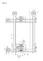
- FIGS. 1 and 2 a thin film transistor array panel according to an exemplary embodiment of the present invention will be described in more detail with reference to FIGS. 1 and 2 .
- FIG. 1 is a plan view layout of a thin film transistor array panel according to an exemplary embodiment of the present invention.
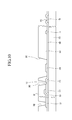
- FIG. 2 is a cross-sectional view of the thin film transistor array panel taken along line II-II of FIG. 1 .
- a plurality of data lines 171 are formed on an insulating substrate 110 which is made of transparent glass, silicone, plastic, or other suitable material.
- the data lines 171 transfer data signals and generally extend in a vertical direction, as illustrated in FIG. 1 .
- Each data line 171 includes a plurality of projections 173 projecting to the side, and a wide end portion 179 for connecting to other layers or an external driving circuit (not shown).
- a data driving circuit (not shown) for generating a data signal may be mounted on a flexible printed circuit film (not shown) attached on the substrate 110, directly mounted on the substrate 110, or integrated with the substrate 110. When the data driving circuit is integrated with the substrate 110, the data line 171 is extended to directly connect thereto.
- the data lines 171 may be made of a low resistance conductor consisting of aluminum containing metals such as aluminum (Al) or an aluminum alloy, silver containing metals such as silver (Ag) or a silver alloy, gold containing metals such as gold (Ag) or a gold alloy, copper containing metals such as copper (Cu) or a copper alloy, molybdenum containing metals such as molybdenum (Mo) or a molybdenum alloy, chrome (Cr), thallium (Ta) and titanium (Ti).
- the data lines 171 may have a multiple film structure including two conductive films (not shown) having different physical properties.
- the sides of the data line 171 are inclined relative to the surface of the substrate 110, and the inclination angles are desirably about 30° to about 80°.
- the interlayer insulating film 160 is formed on the data line 171.
- the interlayer insulating film 160 may be made of a non-organic insulator, such as silicon nitride ("SiNx") or silicon oxide ("SiO 2 "), and a thickness thereof may be about 2000 ⁇ to about 5000 ⁇ .
- the interlayer insulating film 160 has a plurality of contact holes 163 and 162 for exposing each of a projection 173 and an end portion 179, respectively, of the data line 171.
- a plurality of gate lines 121 are formed on the interlayer insulating film 160.
- the gate lines 121 transfer gate signals and generally extend in a horizontal direction to intersect the data lines 171, as illustrated in FIG. 1 .
- Each gate line 121 includes a plurality of gate electrodes 124 projecting to the upper side and a wide end portion 129 for connecting to other layers or an external driving circuit (not shown).
- a gate driving circuit (not shown) for generating a gate signal may be mounted on a flexible printed circuit film (not shown) that is attached on the substrate 110, directly mounted on the substrate 110, or integrated with the substrate 110. When the gate driving circuit is integrated with the substrate 110, the gate line 121 extends to directly connect to the gate driving circuit.
- the gate line 121 may be made of a conductive material that is selected from the same conductive materials for the data line 171.
- the sides of the data line 171 are inclined relative to the surface of the substrate 110, and the inclination angles are desirable about 30° to about 80°.
- An insulating bank 361 is formed on the entire surface of the substrate including the gate line 121 and the interlayer insulating film 160.
- the insulating bank 361 may be made of a photosensitive organic material which can perform a solution process, and a thickness thereof may be about 5000 ⁇ to about 4 ⁇ m.
- the insulating bank 361 has a plurality of openings 365 and a plurality of contact holes 363 and 369.
- Each opening 365 has a cross shape in which a horizontal part 366 is formed along a horizontal direction and a vertical part 367 is formed along a vertical direction, as illustrated in FIG. 1 , intersecting and exposing the gate electrode 124.
- a gate insulating member 140 is formed in the opening 365.
- the gate insulating member 140 fills the entire opening 365 formed in a cross shape.
- the gate insulating member 140 is made of an organic material or an inorganic material having a relative high dielectric constant.
- the organic material includes, for example, a soluble polymer such as polyimide, polyvinyl alcohol, polyfluorane, or parylene.
- the inorganic material includes, for example, silicon oxide whose surface is processed with octadecyl trichloro silane ("OTS").
- the contact holes 363 and 369 expose the projection 173 of the data line 171 and the end portion 129 of the gate line 121, respectively.
- a plurality of connection electrodes 192, a plurality of pixel electrodes 191, and a plurality of contact assistants 81 and 82 are formed on the insulating bank 361 and the gate insulating member 140.
- connection electrode 192 may have an island shape.
- the connection electrode 192 includes a connection part 194 formed in a part of the horizontal part 366 of the opening 365 and is connected to the data line 171 through the contact holes 163 and 363 and a portion (hereinafter, referred to as a 'source electrode') 193 formed along the vertical part 367 of the opening 365.
- the pixel electrode 191 includes a part (hereinafter, referred to as a 'drain electrode') 195 formed along the vertical part 367 of the opening 365 and is opposite to the source electrode 193 about the gate electrode 124.
- a 'drain electrode' part formed along the vertical part 367 of the opening 365 and is opposite to the source electrode 193 about the gate electrode 124.
- the pixel electrode 191 which receives a data voltage from a TFT and a common electrode (not shown) of another array panel (not shown) which receives a common voltage generate an electrical field, thereby determining a direction of liquid crystal molecules of a liquid crystal layer (not shown) between two electrodes.
- the pixel electrode 191 and the common electrode constitute a capacitor (hereinafter, referred to as a "liquid crystal capacitor"), the pixel electrode 191 and the common electrode maintain an applied voltage even after the TFT is turned off.
- an aperture ratio can be increased.
- Contact assistants 81 and 82 are connected to the end portion 129 of the gate line 121 and the end portion 179 of the data line 171 through the contact holes 369 and 162, respectively.
- the contact assistants 81 and 82 compensate adhesion between the end portion 129 of the gate line 121 and the end portion 179 of the data line 171 and an external apparatus (not shown) and protect them.
- the source electrode 193, the pixel electrode 191, and the contact assistants 81 and 82 are made of a transparent conductive material such as indium zinc oxide (“IZO”) or indium tin oxide (“ITO”), and a thickness thereof may be about 300 ⁇ to about 2000 ⁇ .
- IZO indium zinc oxide
- ITO indium tin oxide
- a plurality of organic semiconductors 154 are formed in the opening 365 of the insulating bank 361.
- the organic semiconductor 154 is formed along the vertical part 367 of the opening 365, and is indicated with hatched lines in FIG. 1 .
- the organic semiconductor 154 is in contact with the source electrode 193 and the drain electrode 195, and because a height of the organic semiconductor 154 is lower than that of the insulating bank 361, the organic semiconductor 154 is completely surrounded by the insulating bank 361. Because a side surface of the organic semiconductor 154 is not exposed as the organic semiconductor 154 is completely surrounded by the insulating bank 361, a chemical solution can be prevented from penetrating the side surface of the organic semiconductor 154 in a subsequent process.
- the organic semiconductor 154 may include a high molecular weight compound or a low molecular weight compound that is soluble in an aqueous solution or an organic solvent.
- the organic semiconductor 154 may include a derivative including a substituent such as tetracene or pentacene.
- the organic semiconductor 154 may also include oligothiophene including 4 to 8 thiophenes connected to a position 2 and 5 of a thiophene ring.
- the organic semiconductor 154 may include polythienylenevinylene, poly 3-hexylthiophene, polythiophene, phthalocyanine, metallized phthalocyanine, or a halogen derivative thereof.
- the organic semiconductor 154 may also include perylenetetracarboxylic dianhydride ("PTCDA”), naphthalenetetracarboxylic dianhydride (“NTCDA”), or their imide derivatives.
- PTCDA perylenetetracarboxylic dianhydride
- NTCDA naphthalenetetracarboxylic dianhydride
- the organic semiconductor 154 may also include a derivative including perylene or coronene and their substituents.
- a thickness of the organic semiconductor 154 may be about 300 ⁇ to about 3000 ⁇ .
- a thickness of the insulating bank 361 is larger than the sum of a thickness of the gate insulating member 140 and a thickness of the organic semiconductor 154, side surfaces of the gate insulating member 140 and the organic semiconductor 154 are completely surrounded by the insulating bank 361.
- One gate electrode 124, one source electrode 193, one drain electrode 195 and an organic semiconductor 154 constitute one TFT.
- a channel Q ( FIG. 1 ) of the TFT is formed in the organic semiconductor 154 between the source electrode 193 and the drain electrode 195.
- a protection member 180 is formed on the organic semiconductor 154.
- the protection member 180 for protecting an OTFT can be formed on a partial surface or the entire surface of the substrate, and alternatively, may be omitted.
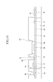
- FIGS. 1 and 2 Now, a method of manufacturing an organic thin film transistor array panel shown in FIGS. 1 and 2 will be described in more detail with reference to FIGS. 3 to 18 .
- FIGS. 3 , 5 , 7 , 9 , 14 , and 17 are plan view layouts sequentially illustrating a method of manufacturing the thin film transistor array panel of FIGS. 1 and 2 according to an exemplary embodiment of the present invention.
- FIG. 4 is a cross-sectional view of the thin film transistor array panel taken along line IV-IV of FIG. 3 .
- FIG. 6 is a cross-sectional view of the thin film transistor array panel taken along line VI-VI of FIG. 5 .
- FIG. 8 is a cross-sectional view of the thin film transistor array panel taken along line VIII-VIII of FIG. 7 .
- FIG. 10 is a cross-sectional view of the thin film transistor array panel taken along line X-X of FIG. 9 .
- FIG. 11A and 11B are schematic plan views sequentially illustrating a state of dropping a gate insulating solution into an opening, which is an enlarged portion 'A' of FIG. 1 .
- FIG. 12 is a schematic plan view illustrating a process margin range of an opening where a gate insulating solution can be.
- FIG. 13 is a cross-sectional view of the thin film transistor array panel formed according to FIGS. 11A to 12 .
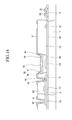
- FIG. 15 is a cross-sectional view of the thin film transistor array panel taken along line XV-XV of FIG. 14 .
- FIG. 16 is a schematic plan view illustrating a process margin area where a gate insulating solution can be dropped.
- FIG. 18 is a cross-sectional view of the thin film transistor array panel taken along line XVIII-XVIII of FIG. 17 .
- conductive layers are formed on the substrate 110 using a method such as sputtering, for example, and the data line 171 including the projection 173 and the end portion 179 are formed by performing a photolithography and etching process on the conductive layer.
- an interlayer insulating film 160 is formed by processing SiNx with a chemical vapor deposition ("CVD") method, and contact holes 162 and 163 are formed by coating a photosensitive film on the interlayer insulating film 160 and performing a photolithography and etching process on the photosensitive film.
- CVD chemical vapor deposition
- the gate line 121 including the gate electrode 124 and the end portion 129 are formed.
- the insulating bank 361 having a plurality of openings 365 and a plurality of contact holes 363 and 369 is formed.
- the opening 365 is formed in a cross shape consisting of the horizontal part 366 that is formed long in a horizontal direction and the vertical part 367 that is formed long in a vertical direction, as illustrated in FIG. 9 .
- the insulating bank 361 is formed having a thickness larger than a desired thickness, for example, having a thickness of about 20,000 ⁇ to about 30,000 ⁇ .
- a surface of the insulating bank 361 is treated.
- Surface treatment is a technique of changing a surface of a material to have a hydrophilic property or a hydrophobic property using plasma.
- the insulating bank 361 is processed with a fluorine-containing gas in a plasma atmosphere.
- a fluorine-containing gas such as CF 4 , C 2 F 6 , or SF 6 is supplied along with oxygen gas (O 2 ) and/or an inert gas.
- the surface of the insulating bank 361 is processed with fluorine, and as the gate electrode 124 and the interlayer insulating film 160 which are exposed through the opening 365 are made of an inorganic material, the gate electrode 124 and the interlayer insulating film 160 are not processed with fluorine.
- the surface of the insulating bank 361 is processed with fluorine, the surface of the insulating bank 361 is treated to have a hydrophobic property, and a portion exposed through the opening 365 has a relatively hydrophilic property.
- the gate insulating member 140 is formed in the opening 365.
- the gate insulating member 140 can be formed with an inkjet printing method, and this will be described with reference to FIGS. 11A to 13 .
- FIGS. 11A and 11B are schematic plan views sequentially illustrating a state of dropping depositing a gate insulating solution in the opening 365, which is an enlarged portion 'A' of FIG. 1 .
- a gate insulating solution 140a As shown in FIG. 11A , several droplets of a gate insulating solution 140a are dropped along the vertical part 367 of the opening 365.
- the gate insulating solution 140a is dropped along a direction J2.
- a hydrophilic gate insulating solution 140a gathers within the opening 365 having a relatively hydrophilic property when droplets of the gate insulating solution 140a are dropped along a direction of the vertical part 367 as in a direction indicated by J1 or J3.
- FIG. 11B several droplets of a gate insulating solution 140b are dropped along the horizontal part 366 of the opening 365.
- the gate insulating solution 140b is dropped along a direction K2.
- the hydrophilic gate insulating solution 140b gathers within the opening 365.
- FIG. 12 is a schematic plan view illustrating a process margin range of an opening where a gate insulating solution can be dropped. Even if a gate insulating solution is not accurately sprayed within the opening 365, the solution can be gathered into the opening 365 depending on surface treatment of the insulating bank 361 when the solution is sprayed to only J1 - J3 or K1 - K3 area. Accordingly, as an area where the gate insulating solution can be dropped is widened, a process margin can be increased.
- the gate insulating member 140 is formed in the opening 365 as shown in FIG. 13 .
- connection electrode 192 including the source electrode 193 and the connection part 194, contact assistants 81 and 82, and the pixel electrode 191 including a drain electrode 195 are formed.
- the organic semiconductor solution 154a is dropped along a direction L2.
- the hydrophilic organic semiconductor solution 140a gathers within the opening 365 having a relatively hydrophilic property when the solution is dropped in the same direction as the vertical part 367, as in a direction L1 or L3. Accordingly, as an area where the organic semiconductor solution 154a can be dropped is widened, a process margin can be increased.
- the organic semiconductor solution 154a is not dropped along the horizontal part 366 of the opening 365.
- the gate insulating member 140 and the organic semiconductor 154 are formed in one opening 365. Therefore, when both the gate insulating member 140 and the organic semiconductor 154 are formed by an inkjet printing method, the number of masks required for forming a separate insulating bank to surround each of them can be reduced by one.
- the organic semiconductor solution having a hydrophilic property can be overflowed along the connection electrode 192 and the pixel electrode 191 which are positioned in the lower part of the opening.
- the opening 365 is formed in a cross shape consisting of the horizontal part 366 and the vertical part 367, and the organic semiconductor solution 154a is dropped into only the vertical part 367 formed along a portion in which a channel (Q) of the TFT is formed, whereby the organic semiconductor solution 154a can be prevented from overflowing to the connection part 194 and/or the pixel electrode 191 side regardless of the channel (Q).
- the organic semiconductor 154 is formed in the opening 365, as shown in FIGS. 17 and 18 .
- a passivation layer 180 for covering the organic semiconductor 154 is formed by coating an insulating film on the entire surface of the substrate 110 and performing a photolithography process on the insulating film.
- the number of masks required for forming a separate insulating bank can be reduced and a process margin of inkjet spraying can be increased by performing surface treatment of the insulating bank. Furthermore, by adjusting a shape of an opening of the insulating bank, a solution can be prevented from overflowing and characteristics of a TFT can be prevented from deteriorating.
Landscapes
- Engineering & Computer Science (AREA)
- Microelectronics & Electronic Packaging (AREA)
- Physics & Mathematics (AREA)
- Geometry (AREA)
- Manufacturing & Machinery (AREA)
- Thin Film Transistor (AREA)
- Liquid Crystal (AREA)
Applications Claiming Priority (2)
| Application Number | Priority Date | Filing Date | Title |
|---|---|---|---|
| KR1020060052008A KR101187205B1 (ko) | 2006-06-09 | 2006-06-09 | 박막 트랜지스터 표시판 및 그 제조 방법 |
| EP07010837A EP1865558A3 (fr) | 2006-06-09 | 2007-06-01 | Panneau à réseau de transistors à couche mince et son procédé de fabrication |
Related Parent Applications (1)
| Application Number | Title | Priority Date | Filing Date |
|---|---|---|---|
| EP07010837A Division EP1865558A3 (fr) | 2006-06-09 | 2007-06-01 | Panneau à réseau de transistors à couche mince et son procédé de fabrication |
Publications (2)
| Publication Number | Publication Date |
|---|---|
| EP2690663A2 true EP2690663A2 (fr) | 2014-01-29 |
| EP2690663A3 EP2690663A3 (fr) | 2014-07-23 |
Family
ID=38521797
Family Applications (2)
| Application Number | Title | Priority Date | Filing Date |
|---|---|---|---|
| EP13189781.1A Withdrawn EP2690663A3 (fr) | 2006-06-09 | 2007-06-01 | Procédé de fabrication d'un panneau d'affichage de transistor à couche mince |
| EP07010837A Ceased EP1865558A3 (fr) | 2006-06-09 | 2007-06-01 | Panneau à réseau de transistors à couche mince et son procédé de fabrication |
Family Applications After (1)
| Application Number | Title | Priority Date | Filing Date |
|---|---|---|---|
| EP07010837A Ceased EP1865558A3 (fr) | 2006-06-09 | 2007-06-01 | Panneau à réseau de transistors à couche mince et son procédé de fabrication |
Country Status (5)
| Country | Link |
|---|---|
| US (1) | US7781774B2 (fr) |
| EP (2) | EP2690663A3 (fr) |
| JP (1) | JP5268290B2 (fr) |
| KR (1) | KR101187205B1 (fr) |
| CN (1) | CN101086996B (fr) |
Families Citing this family (13)
| Publication number | Priority date | Publication date | Assignee | Title |
|---|---|---|---|---|
| KR20070053060A (ko) * | 2005-11-19 | 2007-05-23 | 삼성전자주식회사 | 표시장치와 이의 제조방법 |
| JP5151172B2 (ja) * | 2007-02-14 | 2013-02-27 | ソニー株式会社 | 画素回路および表示装置 |
| GB0803702D0 (en) | 2008-02-28 | 2008-04-09 | Isis Innovation | Transparent conducting oxides |
| KR101124545B1 (ko) * | 2008-02-29 | 2012-03-15 | 고려대학교 산학협력단 | 유기 박막 트랜지스터 및 그 제조 방법 |
| CN101710586B (zh) * | 2009-01-09 | 2011-12-28 | 深超光电(深圳)有限公司 | 提高开口率的储存电容及其制作方法 |
| GB0915376D0 (en) | 2009-09-03 | 2009-10-07 | Isis Innovation | Transparent conducting oxides |
| CN102034750B (zh) * | 2009-09-25 | 2015-03-11 | 北京京东方光电科技有限公司 | 阵列基板及其制造方法 |
| JP5621273B2 (ja) * | 2010-02-23 | 2014-11-12 | ソニー株式会社 | 薄膜トランジスタ構造体およびその製造方法、ならびに電子機器 |
| CN117410348A (zh) * | 2010-04-23 | 2024-01-16 | 株式会社半导体能源研究所 | 半导体装置和晶体管的制造方法 |
| KR101705367B1 (ko) * | 2010-07-26 | 2017-02-10 | 엘지디스플레이 주식회사 | 유기박막트랜지스터의 제조방법 |
| US9698347B2 (en) * | 2012-08-02 | 2017-07-04 | Joled Inc. | Organic EL display panel and method for manufacturing same |
| JP6242121B2 (ja) * | 2013-09-02 | 2017-12-06 | 株式会社ジャパンディスプレイ | 発光素子表示装置及び発光素子表示装置の製造方法 |
| KR102285384B1 (ko) * | 2014-09-15 | 2021-08-04 | 삼성디스플레이 주식회사 | 박막 트랜지스터 어레이 기판, 그 제조방법 및 표시 장치 |
Family Cites Families (13)
| Publication number | Priority date | Publication date | Assignee | Title |
|---|---|---|---|---|
| KR100608543B1 (ko) * | 1998-03-17 | 2006-08-03 | 세이코 엡슨 가부시키가이샤 | 표시장치의 제조방법 및 박막발광소자의 제조방법 |
| JP3646510B2 (ja) * | 1998-03-18 | 2005-05-11 | セイコーエプソン株式会社 | 薄膜形成方法、表示装置およびカラーフィルタ |
| KR100333983B1 (ko) * | 1999-05-13 | 2002-04-26 | 윤종용 | 광시야각 액정 표시 장치용 박막 트랜지스터 어레이 기판 및그의 제조 방법 |
| KR20050051683A (ko) * | 2002-10-07 | 2005-06-01 | 코닌클리케 필립스 일렉트로닉스 엔.브이. | 발광 디스플레이 제조 방법 |
| JP3788467B2 (ja) * | 2003-05-28 | 2006-06-21 | セイコーエプソン株式会社 | パターン形成方法、デバイス及びデバイスの製造方法、電気光学装置、電子機器並びにアクティブマトリクス基板の製造方法 |
| KR100973811B1 (ko) * | 2003-08-28 | 2010-08-03 | 삼성전자주식회사 | 유기 반도체를 사용한 박막 트랜지스터 표시판 및 그 제조방법 |
| KR100549984B1 (ko) * | 2003-12-29 | 2006-02-07 | 엘지.필립스 엘시디 주식회사 | 듀얼패널타입 유기전계발광 소자 및 그 제조방법 |
| US7022534B2 (en) * | 2004-01-14 | 2006-04-04 | Osram Opto Semiconductors Gmbh | Optimal bank height for inkjet printing |
| KR100658288B1 (ko) | 2004-06-25 | 2006-12-14 | 삼성에스디아이 주식회사 | 개량된 구조의 트랜지스터를 구비한 화소 회로 및 유기발광 표시장치 |
| JP4389747B2 (ja) * | 2004-10-12 | 2009-12-24 | セイコーエプソン株式会社 | パターン形成方法および配線形成方法 |
| KR101090250B1 (ko) * | 2004-10-15 | 2011-12-06 | 삼성전자주식회사 | 유기 반도체를 이용한 박막 트랜지스터 표시판 및 그 제조방법 |
| JP2006251120A (ja) * | 2005-03-09 | 2006-09-21 | Seiko Epson Corp | 画素構造、アクティブマトリクス基板、アクティブマトリクス基板の製造方法、電気光学装置、並びに電子機器 |
| JP5148086B2 (ja) * | 2005-08-18 | 2013-02-20 | 三星電子株式会社 | 有機薄膜トランジスタ表示板 |
-
2006
- 2006-06-09 KR KR1020060052008A patent/KR101187205B1/ko active IP Right Grant
- 2006-11-13 US US11/559,162 patent/US7781774B2/en not_active Expired - Fee Related
- 2006-11-20 CN CN2006101486421A patent/CN101086996B/zh not_active Expired - Fee Related
-
2007
- 2007-06-01 EP EP13189781.1A patent/EP2690663A3/fr not_active Withdrawn
- 2007-06-01 EP EP07010837A patent/EP1865558A3/fr not_active Ceased
- 2007-06-07 JP JP2007151432A patent/JP5268290B2/ja not_active Expired - Fee Related
Non-Patent Citations (1)
| Title |
|---|
| None |
Also Published As
| Publication number | Publication date |
|---|---|
| CN101086996B (zh) | 2011-07-27 |
| JP5268290B2 (ja) | 2013-08-21 |
| US20070284585A1 (en) | 2007-12-13 |
| JP2007335862A (ja) | 2007-12-27 |
| US7781774B2 (en) | 2010-08-24 |
| EP1865558A2 (fr) | 2007-12-12 |
| CN101086996A (zh) | 2007-12-12 |
| EP2690663A3 (fr) | 2014-07-23 |
| KR20070117850A (ko) | 2007-12-13 |
| EP1865558A3 (fr) | 2013-02-13 |
| KR101187205B1 (ko) | 2012-10-02 |
Similar Documents
| Publication | Publication Date | Title |
|---|---|---|
| US7781774B2 (en) | Thin film transistor array panel | |
| US7569851B2 (en) | Organic thin film transistor array panels | |
| KR20070052067A (ko) | 유기 박막 트랜지스터 표시판 및 그 제조 방법 | |
| US20070024766A1 (en) | Organic thin film transistor display panel | |
| US20060197881A1 (en) | Organic thin film transistor array panel and manufacturing method thereof | |
| KR101272328B1 (ko) | 잉크젯 프린팅 시스템 및 이를 이용한 박막 트랜지스터표시판의 제조 방법 | |
| US7994494B2 (en) | Organic thin film transistor array panel and method for manufacturing the same | |
| CN1983620B (zh) | 有机薄膜晶体管阵列面板 | |
| EP1887630A2 (fr) | Panneau à réseau de transistors à couche mince et son procédé de fabrication | |
| US20080076204A1 (en) | Method for manufacturing a thin film transistor array panel | |
| US7759676B2 (en) | Thin film transistor array panel having groups of proximately located thin film transistors and manufacturing method thereof | |
| US20070278492A1 (en) | Thin film transistor array panel and method of manufacturing the same | |
| US20080038881A1 (en) | Thin Film Transistor Array Panel and Manufacturing Method Thereof | |
| KR101251997B1 (ko) | 박막 트랜지스터 표시판 및 그 제조 방법 | |
| KR20070052505A (ko) | 잉크젯 프린팅 시스템 및 이를 이용한 유기 박막트랜지스터 표시판의 제조 방법 | |
| KR20080042441A (ko) | 유기 박막 트랜지스터 표시판 및 그 제조 방법 | |
| KR101272331B1 (ko) | 유기 박막 트랜지스터 표시판 및 그의 제조 방법 | |
| KR20080044436A (ko) | 박막 트랜지스터 표시판 및 그 제조 방법 | |
| KR20080078348A (ko) | 박막 트랜지스터 표시판 및 그 제조 방법 | |
| KR20070096609A (ko) | 박막 트랜지스터 표시판 및 그 제조 방법 | |
| KR20080026236A (ko) | 박막 트랜지스터 표시판 및 그 제조 방법 | |
| KR20070101030A (ko) | 박막 트랜지스터 표시판 및 그 제조 방법 | |
| KR20080082226A (ko) | 유기 박막 트랜지스터 표시판 및 그 제조 방법 |
Legal Events
| Date | Code | Title | Description |
|---|---|---|---|
| PUAI | Public reference made under article 153(3) epc to a published international application that has entered the european phase |
Free format text: ORIGINAL CODE: 0009012 |
|
| AC | Divisional application: reference to earlier application |
Ref document number: 1865558 Country of ref document: EP Kind code of ref document: P |
|
| AK | Designated contracting states |
Kind code of ref document: A2 Designated state(s): AT BE BG CH CY CZ DE DK EE ES FI FR GB GR HU IE IS IT LI LT LU LV MC MT NL PL PT RO SE SI SK TR |
|
| AX | Request for extension of the european patent |
Extension state: AL BA HR MK RS |
|
| RIC1 | Information provided on ipc code assigned before grant |
Ipc: H01L 27/32 20060101AFI20140221BHEP Ipc: H01L 51/05 20060101ALI20140221BHEP Ipc: H01L 51/00 20060101ALI20140221BHEP |
|
| PUAL | Search report despatched |
Free format text: ORIGINAL CODE: 0009013 |
|
| AK | Designated contracting states |
Kind code of ref document: A3 Designated state(s): AT BE BG CH CY CZ DE DK EE ES FI FR GB GR HU IE IS IT LI LT LU LV MC MT NL PL PT RO SE SI SK TR |
|
| AX | Request for extension of the european patent |
Extension state: AL BA HR MK RS |
|
| RIC1 | Information provided on ipc code assigned before grant |
Ipc: H01L 27/32 20060101AFI20140613BHEP Ipc: H01L 51/00 20060101ALI20140613BHEP Ipc: H01L 51/05 20060101ALI20140613BHEP |
|
| 17P | Request for examination filed |
Effective date: 20150116 |
|
| RBV | Designated contracting states (corrected) |
Designated state(s): AT BE BG CH CY CZ DE DK EE ES FI FR GB GR HU IE IS IT LI LT LU LV MC MT NL PL PT RO SE SI SK TR |
|
| RAP1 | Party data changed (applicant data changed or rights of an application transferred) |
Owner name: SAMSUNG DISPLAY CO., LTD. |
|
| 17Q | First examination report despatched |
Effective date: 20161026 |
|
| RIC1 | Information provided on ipc code assigned before grant |
Ipc: H01L 51/40 20060101AFI20170718BHEP Ipc: H01L 27/32 20060101ALI20170718BHEP |
|
| GRAP | Despatch of communication of intention to grant a patent |
Free format text: ORIGINAL CODE: EPIDOSNIGR1 |
|
| INTG | Intention to grant announced |
Effective date: 20170913 |
|
| STAA | Information on the status of an ep patent application or granted ep patent |
Free format text: STATUS: THE APPLICATION IS DEEMED TO BE WITHDRAWN |
|
| 18D | Application deemed to be withdrawn |
Effective date: 20180124 |