EP2686944B1 - Lighting power circuit with peak current limiter for emi filter - Google Patents
Lighting power circuit with peak current limiter for emi filter Download PDFInfo
- Publication number
- EP2686944B1 EP2686944B1 EP12716103.2A EP12716103A EP2686944B1 EP 2686944 B1 EP2686944 B1 EP 2686944B1 EP 12716103 A EP12716103 A EP 12716103A EP 2686944 B1 EP2686944 B1 EP 2686944B1
- Authority
- EP
- European Patent Office
- Prior art keywords
- circuit
- terminal
- output
- coupled
- field effect
- Prior art date
- Legal status (The legal status is an assumption and is not a legal conclusion. Google has not performed a legal analysis and makes no representation as to the accuracy of the status listed.)
- Not-in-force
Links
Images


Classifications
-
- H—ELECTRICITY
- H02—GENERATION; CONVERSION OR DISTRIBUTION OF ELECTRIC POWER
- H02M—APPARATUS FOR CONVERSION BETWEEN AC AND AC, BETWEEN AC AND DC, OR BETWEEN DC AND DC, AND FOR USE WITH MAINS OR SIMILAR POWER SUPPLY SYSTEMS; CONVERSION OF DC OR AC INPUT POWER INTO SURGE OUTPUT POWER; CONTROL OR REGULATION THEREOF
- H02M1/00—Details of apparatus for conversion
- H02M1/44—Circuits or arrangements for compensating for electromagnetic interference in converters or inverters
-
- H—ELECTRICITY
- H02—GENERATION; CONVERSION OR DISTRIBUTION OF ELECTRIC POWER
- H02M—APPARATUS FOR CONVERSION BETWEEN AC AND AC, BETWEEN AC AND DC, OR BETWEEN DC AND DC, AND FOR USE WITH MAINS OR SIMILAR POWER SUPPLY SYSTEMS; CONVERSION OF DC OR AC INPUT POWER INTO SURGE OUTPUT POWER; CONTROL OR REGULATION THEREOF
- H02M1/00—Details of apparatus for conversion
- H02M1/14—Arrangements for reducing ripples from DC input or output
- H02M1/15—Arrangements for reducing ripples from DC input or output using active elements
-
- H—ELECTRICITY
- H03—ELECTRONIC CIRCUITRY
- H03H—IMPEDANCE NETWORKS, e.g. RESONANT CIRCUITS; RESONATORS
- H03H1/00—Constructional details of impedance networks whose electrical mode of operation is not specified or applicable to more than one type of network
- H03H1/0007—Constructional details of impedance networks whose electrical mode of operation is not specified or applicable to more than one type of network of radio frequency interference filters
-
- H—ELECTRICITY
- H05—ELECTRIC TECHNIQUES NOT OTHERWISE PROVIDED FOR
- H05B—ELECTRIC HEATING; ELECTRIC LIGHT SOURCES NOT OTHERWISE PROVIDED FOR; CIRCUIT ARRANGEMENTS FOR ELECTRIC LIGHT SOURCES, IN GENERAL
- H05B41/00—Circuit arrangements or apparatus for igniting or operating discharge lamps
- H05B41/14—Circuit arrangements
- H05B41/36—Controlling
- H05B41/38—Controlling the intensity of light
- H05B41/39—Controlling the intensity of light continuously
- H05B41/392—Controlling the intensity of light continuously using semiconductor devices, e.g. thyristor
- H05B41/3921—Controlling the intensity of light continuously using semiconductor devices, e.g. thyristor with possibility of light intensity variations
-
- H—ELECTRICITY
- H05—ELECTRIC TECHNIQUES NOT OTHERWISE PROVIDED FOR
- H05B—ELECTRIC HEATING; ELECTRIC LIGHT SOURCES NOT OTHERWISE PROVIDED FOR; CIRCUIT ARRANGEMENTS FOR ELECTRIC LIGHT SOURCES, IN GENERAL
- H05B45/00—Circuit arrangements for operating light-emitting diodes [LED]
-
- H—ELECTRICITY
- H05—ELECTRIC TECHNIQUES NOT OTHERWISE PROVIDED FOR
- H05B—ELECTRIC HEATING; ELECTRIC LIGHT SOURCES NOT OTHERWISE PROVIDED FOR; CIRCUIT ARRANGEMENTS FOR ELECTRIC LIGHT SOURCES, IN GENERAL
- H05B45/00—Circuit arrangements for operating light-emitting diodes [LED]
- H05B45/30—Driver circuits
- H05B45/31—Phase-control circuits
-
- H—ELECTRICITY
- H05—ELECTRIC TECHNIQUES NOT OTHERWISE PROVIDED FOR
- H05B—ELECTRIC HEATING; ELECTRIC LIGHT SOURCES NOT OTHERWISE PROVIDED FOR; CIRCUIT ARRANGEMENTS FOR ELECTRIC LIGHT SOURCES, IN GENERAL
- H05B45/00—Circuit arrangements for operating light-emitting diodes [LED]
- H05B45/30—Driver circuits
- H05B45/36—Circuits for reducing or suppressing harmonics, ripples or electromagnetic interferences [EMI]
-
- H—ELECTRICITY
- H05—ELECTRIC TECHNIQUES NOT OTHERWISE PROVIDED FOR
- H05B—ELECTRIC HEATING; ELECTRIC LIGHT SOURCES NOT OTHERWISE PROVIDED FOR; CIRCUIT ARRANGEMENTS FOR ELECTRIC LIGHT SOURCES, IN GENERAL
- H05B45/00—Circuit arrangements for operating light-emitting diodes [LED]
- H05B45/30—Driver circuits
- H05B45/37—Converter circuits
-
- H—ELECTRICITY
- H05—ELECTRIC TECHNIQUES NOT OTHERWISE PROVIDED FOR
- H05B—ELECTRIC HEATING; ELECTRIC LIGHT SOURCES NOT OTHERWISE PROVIDED FOR; CIRCUIT ARRANGEMENTS FOR ELECTRIC LIGHT SOURCES, IN GENERAL
- H05B45/00—Circuit arrangements for operating light-emitting diodes [LED]
- H05B45/30—Driver circuits
- H05B45/355—Power factor correction [PFC]; Reactive power compensation
Definitions
- Integral electronic lamps such as compact fluorescent designs (CFLs) and LED lamps can be used in conventional lamps designed for incandescent bulbs and may include dimming circuitry allowing the light output to be adjusted by phase-cut dimming (triac control).
- trimming circuitry allowing the light output to be adjusted by phase-cut dimming (triac control).
- the triac operation of such dimmer controls applies a fast step change in the voltage across the EMI filter capacitor, leading to current spikes in the capacitor and in the power line. This can cause degradation of the EMI filter capacitor and can also damage the dimmer triac.
- Figs. 1 and 2 illustrate two exemplary electronic circuits 100 for powering lighting devices. These power circuits 100 each include an input rectifier 101 receiving signal or multi-phase AC input power from an external source, as well as an EMI filter 102 coupled to the DC side of the rectifier 101.
- the rectifier circuit 101 in certain embodiments is a full wave rectifier type, including four diode rectifiers formed into a bridge circuit for single-phase inputs, or 6 or more rectifiers for multi-phase inputs. In other embodiments, the rectifier circuit 101 can be a half-wave rectifier or a single diode.
- the circuits 100 of Figs. 1 and 2 also include a power converter circuit 110 including one or more DC to DC converters for directly or indirectly powering at least one light source 108.
- the circuit 100 is an LED driver with the power converter 110 including a boost-type DC-DC converter stage 104 followed by a buck DC-DC converter 106 that provides a DC output to drive one or more LED lighting devices 108.
- Other forms of DC-DC converter may be used for the second circuit 106, such as a flyback converter with an isolation transformer, a buck-boost converter, etc.
- the boost converter 1004 provides DC to an inverter (not shown), which in turn drives an isolation transformer primary whose secondary winding drives an output rectifier connected to an LED array.
- the circuit 100 of Fig. 2 forms an electronic ballast, and includes an inverter 107 receiving a DC output from the boost converter 104 and providing an AC output to power one or more fluorescent lamps 108.
- one of the DC-DC converter stages may be omitted, and in some embodiments, the initial DC-DC converter stage 104 operates to provide power factor correction functions.
- one or more of the converter stages 104, 106, 107 may provide for dimming control to modify the output power applied to the light source(s) 108 based on a dimming input (not shown).
- the driver or ballast 100 may be powered from a single-phase AC source with dimming control via a phase-cut dimmer 200 coupled in series with the AC source and the driver 100.
- the dimmer control 200 includes a triac T201 that selectively cuts or interrupts current flow in portions of each cycle of the AC source 101 (phase cutting) to dim the light output according to a user-adjustable resistance R201.
- the driver or ballast circuit 100 may be housed in a structure having an Edison base with AC input terminals.
- the rectifier circuit 101 has AC input terminals for connection to an external source to receive the AC input power, and provides a rectified DC output at first and second DC output terminals 101a and 101b, respectively.
- This rectifier output 101a, 101b is coupled to first and second input terminals of the EMI filter circuit 102.
- the filter circuit 102 includes output terminals 102a and 102b that are coupled to provide the DC input to the initial (e.g., boost) DC-DC converter 104.
- the output of the boost converter 104 provides DC power at the input of the buck converter 106, and its output is used to directly drive LED light source(s) 108 (e.g., Fig. 1 ) or the boost converter output is used to indirectly power one or more fluorescent lamps 108 via an inverter ( Fig. 2 ).
- the EMI filter circuit 102 in Figs. 1 and 2 includes an inductor L1 coupled in the upper (positive) DC branch, as well as a capacitor C1 connected in series with an N-channel depletion mode field effect transistor (FET) Q1 in a circuit branch extending between the upper and lower rectifier output terminals 101a and 101b, respectively.
- the filter capacitance C1 has a first terminal coupled with the positive DC rectifier output terminal and a second terminal connected to a first source/drain terminal SD1 of the FET Q1, with the inductor L1 extending between the positive DC rectifier output 101a and the upper filter output terminal 102a.
- the other source/drain terminal SD2 of Q1 is connected to the negative DC output terminal 101b of the rectifier circuit 101, as is the FET gate terminal G.
- the filter circuit 102 provides EMI filtering in operation with application of fully sinusoidal AC input power to the rectifier 101.
- the inductor L1 has an inductance of approximately 25 mH, which is large enough so that the EMI current at about 150 KHz is relatively small (e.g., about 10-20 ma of EMI current), and the EMI filter capacitor is about 15 nF, where the EMI filtering ideally provides low pass filtering of interference frequencies of about 150 KHz or more.
- increasing the capacitance of C1 would advantageously improve the EMI filtering capabilities of the circuit 102.
- a larger capacitance for C1 exacerbates the magnitude of current spikes resulting from the mid-cycle firing of the dimming triac T201, absent provision of countermeasures set forth in the present disclosure.
- the filter circuit 102 in Figs. 1 and 2 provides an impedance via the FET Q1 in series with the filter capacitor C1.
- the depletion mode device Q1 is normally on (conductive drain-source channel condition) for non-phase-cutting operation, and the series drain-to-source resistance RDS ON is exemplified in the graph 400 which shows drain-source current curves (I DS ) as a function of gate-source voltage V GS for Q1. Since the FET in the embodiments of Figs.
- Q1 is a depletion mode device
- Q1 has a negative threshold voltage V T and a non-zero current (about 300-400 ma in one example) conducts when the gate and source are shorted together.
- V T negative threshold voltage
- a non-zero current about 300-400 ma in one example
- I DS channel current levels
- Q1 is chosen to have an RDS ON of about 2-10 ⁇ in the depleted mode at the zero V GS of about 1/3 to 1/2 of the reactance (1/ ⁇ C) of the capacitor, where ⁇ is 150KHz with respect to the switching frequency of the power converter stage 110.
- the circuit 102 filters, and when the triac T201 fires, the FET Q1 comes out of saturation and limits the spike current to a few hundred ma.
- the design of Figs. 1 and 2 is not a fixed resistor in the capacitor circuit, but instead a variable impedance is provided which clamps the maximum current.
- an N-channel depletion mode FET Q1 is used, having a 250 volt rating and a rated RDS ON of about 5 ⁇ can be used. It is noted that the use of the variable impedance FET Q1 can facilitate increasing the capacitance of C1 to facilitate improved EMI filtering, with the FET Q1 providing current limiting to mitigate capacitor or triac degradation.
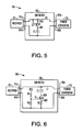
- Fig. 5 shows another embodiment of an EMI filter circuit 102 that can be used in driver or ballast type circuits (e.g., Figs. 1 or 2 above).
- a P-channel depletion mode FET Q1 is used, with a first source/drain SD1 connected to the upper capacitor terminal of C1, and with the other source/drain SD2 connected to the upper (positive) rectifier DC output terminal 101a.
- the gate is also connected to the upper DC rail, and the device Q1 provides an on-state resistance RDS ON (e.g., about 2-10 ⁇ ) for filtering and current spike protection.
- an enhancement mode FET Q1 can be used, such as an N-channel device shown in the figure.
- a bias circuit is provided to set the gate voltage, in this case including a first resistor R1 connected between the gate G and a positive Dc voltage VCC (e.g., 15 volts in one example), with a second resistor R2 connected from the gate G to the lower (negative) DC rectifier output.
- VCC positive Dc voltage
- the gate voltage is biased by the circuit R1, R2 to about 4 volts for a Q1 threshold voltage V T of about 3 volts.
- this connection of an enhancement mode device in series with the capacitor C1 provides an RDS ON (e.g., about 2-10 ⁇ ) for filtering and implements current spike protection as the V DS increases.
- a third resistor R3 can be provided between the lower source/drain SD1 and the lower DC terminal 101b, such as a 2 ⁇ resistor in one example, so as to allow approximately 500 ma of current flow in the capacitor C1.
- a zener diode can be used in the bias circuit (e.g., a device with a zener voltage V Z of about 4v between the FET gate and ground).
Landscapes
- Physics & Mathematics (AREA)
- Electromagnetism (AREA)
- Engineering & Computer Science (AREA)
- Power Engineering (AREA)
- Circuit Arrangement For Electric Light Sources In General (AREA)
- Power Conversion In General (AREA)
- Filters And Equalizers (AREA)
- Networks Using Active Elements (AREA)
- Dc-Dc Converters (AREA)
Applications Claiming Priority (2)
| Application Number | Priority Date | Filing Date | Title |
|---|---|---|---|
| US13/047,914 US8461774B2 (en) | 2011-03-15 | 2011-03-15 | Lighting power circuit with peak current limiter for EMI filter |
| PCT/US2012/026514 WO2012161795A1 (en) | 2011-03-15 | 2012-02-24 | Lighting power circuit with peak current limiter for emi filter |
Publications (2)
| Publication Number | Publication Date |
|---|---|
| EP2686944A1 EP2686944A1 (en) | 2014-01-22 |
| EP2686944B1 true EP2686944B1 (en) | 2015-08-26 |
Family
ID=45998618
Family Applications (1)
| Application Number | Title | Priority Date | Filing Date |
|---|---|---|---|
| EP12716103.2A Not-in-force EP2686944B1 (en) | 2011-03-15 | 2012-02-24 | Lighting power circuit with peak current limiter for emi filter |
Country Status (8)
| Country | Link |
|---|---|
| US (1) | US8461774B2 (enExample) |
| EP (1) | EP2686944B1 (enExample) |
| JP (1) | JP6200810B2 (enExample) |
| KR (1) | KR101932172B1 (enExample) |
| CN (1) | CN103493348B (enExample) |
| BR (1) | BR112013021955A2 (enExample) |
| MX (1) | MX2013010567A (enExample) |
| WO (1) | WO2012161795A1 (enExample) |
Families Citing this family (34)
| Publication number | Priority date | Publication date | Assignee | Title |
|---|---|---|---|---|
| US8704460B2 (en) * | 2011-11-07 | 2014-04-22 | Maxim Integrated Products, Inc. | LED current control in a dimmable LED illumination system |
| US8872426B2 (en) * | 2012-11-26 | 2014-10-28 | Lucidity Lights, Inc. | Arrangements and methods for triac dimming of gas discharge lamps powered by electronic ballasts |
| US10128101B2 (en) | 2012-11-26 | 2018-11-13 | Lucidity Lights, Inc. | Dimmable induction RF fluorescent lamp with reduced electromagnetic interference |
| US9209008B2 (en) | 2012-11-26 | 2015-12-08 | Lucidity Lights, Inc. | Fast start induction RF fluorescent light bulb |
| US9305765B2 (en) | 2012-11-26 | 2016-04-05 | Lucidity Lights, Inc. | High frequency induction lighting |
| US20140375203A1 (en) | 2012-11-26 | 2014-12-25 | Lucidity Lights, Inc. | Induction rf fluorescent lamp with helix mount |
| US10529551B2 (en) | 2012-11-26 | 2020-01-07 | Lucidity Lights, Inc. | Fast start fluorescent light bulb |
| US8941304B2 (en) | 2012-11-26 | 2015-01-27 | Lucidity Lights, Inc. | Fast start dimmable induction RF fluorescent light bulb |
| US9161422B2 (en) | 2012-11-26 | 2015-10-13 | Lucidity Lights, Inc. | Electronic ballast having improved power factor and total harmonic distortion |
| US10141179B2 (en) | 2012-11-26 | 2018-11-27 | Lucidity Lights, Inc. | Fast start RF induction lamp with metallic structure |
| US9245734B2 (en) | 2012-11-26 | 2016-01-26 | Lucidity Lights, Inc. | Fast start induction RF fluorescent lamp with burst-mode dimming |
| US9460907B2 (en) | 2012-11-26 | 2016-10-04 | Lucidity Lights, Inc. | Induction RF fluorescent lamp with load control for external dimming device |
| US9129792B2 (en) | 2012-11-26 | 2015-09-08 | Lucidity Lights, Inc. | Fast start induction RF fluorescent lamp with reduced electromagnetic interference |
| US9524861B2 (en) | 2012-11-26 | 2016-12-20 | Lucidity Lights, Inc. | Fast start RF induction lamp |
| US9129791B2 (en) | 2012-11-26 | 2015-09-08 | Lucidity Lights, Inc. | RF coupler stabilization in an induction RF fluorescent light bulb |
| AT13688U1 (de) * | 2012-12-06 | 2014-06-15 | Tridonic Gmbh & Co Kg | Betriebsgerät für Leuchtmittel |
| AT13872U1 (de) * | 2013-05-02 | 2014-10-15 | Tridonic Gmbh & Co Kg | Betriebsgerät für Leuchtmittel |
| USD745981S1 (en) | 2013-07-19 | 2015-12-22 | Lucidity Lights, Inc. | Inductive lamp |
| USD745982S1 (en) | 2013-07-19 | 2015-12-22 | Lucidity Lights, Inc. | Inductive lamp |
| USD746490S1 (en) | 2013-07-19 | 2015-12-29 | Lucidity Lights, Inc. | Inductive lamp |
| USD747009S1 (en) | 2013-08-02 | 2016-01-05 | Lucidity Lights, Inc. | Inductive lamp |
| USD747507S1 (en) | 2013-08-02 | 2016-01-12 | Lucidity Lights, Inc. | Inductive lamp |
| CN104753338B (zh) * | 2013-12-25 | 2018-03-23 | 台达电子企业管理(上海)有限公司 | 电力电子电路与功率模块 |
| FR3034929B1 (fr) * | 2015-04-08 | 2019-03-22 | Schneider Electric Industries Sas | Systeme de filtrage actif |
| CN105101556B (zh) * | 2015-08-21 | 2017-12-12 | 京东方光科技有限公司 | Led 调光驱动电路 |
| CN105553244B (zh) * | 2015-12-22 | 2018-05-29 | 矽力杰半导体技术(杭州)有限公司 | Emi滤波器及应用其的开关电源 |
| WO2017139299A1 (en) * | 2016-02-08 | 2017-08-17 | Hubbell Incorporated | Multiphase light fixture |
| US10873270B2 (en) * | 2017-03-23 | 2020-12-22 | Eaton Intelligent Power Limited | Converter apparatus using source-activated discharge circuits |
| US10236174B1 (en) | 2017-12-28 | 2019-03-19 | Lucidity Lights, Inc. | Lumen maintenance in fluorescent lamps |
| USD854198S1 (en) | 2017-12-28 | 2019-07-16 | Lucidity Lights, Inc. | Inductive lamp |
| CN108337774B (zh) * | 2018-02-07 | 2024-06-28 | 珠海世讯科技有限公司 | 一种大功率mosfet调光电路 |
| US11528789B2 (en) * | 2020-09-14 | 2022-12-13 | ERP Power, LLC | Negative injection for power factor correction circuit performance enhancements |
| EP4047768A1 (en) * | 2021-02-18 | 2022-08-24 | Schaffner EMV AG | Electromagnetic compatibility filter having controlled impedance magnitude |
| CN115996033A (zh) * | 2023-03-22 | 2023-04-21 | 敏业信息科技(上海)有限公司 | 一种电磁干扰滤波器 |
Family Cites Families (15)
| Publication number | Priority date | Publication date | Assignee | Title |
|---|---|---|---|---|
| JPH09214276A (ja) * | 1996-02-05 | 1997-08-15 | Tohoku Ricoh Co Ltd | ノイズフィルタ |
| WO2000056121A1 (en) * | 1999-03-12 | 2000-09-21 | Koninklijke Philips Electronics N.V. | Circuit arrangement and signal light provided with said circuit arrangement |
| US6373200B1 (en) | 2000-07-31 | 2002-04-16 | General Electric Company | Interface circuit and method |
| DE10163034B4 (de) * | 2001-12-20 | 2014-08-28 | Tridonic Gmbh & Co Kg | Elektronisches Vorschaltgerät mit Überspannungsüberwachung |
| JP5110847B2 (ja) * | 2005-10-18 | 2012-12-26 | 株式会社半導体エネルギー研究所 | 表示装置 |
| US7868561B2 (en) | 2007-10-31 | 2011-01-11 | Lutron Electronics Co., Inc. | Two-wire dimmer circuit for a screw-in compact fluorescent lamp |
| US8199541B2 (en) * | 2008-04-11 | 2012-06-12 | System General Corp. | High efficiency bridgeless PFC power converter |
| JP2009260615A (ja) * | 2008-04-16 | 2009-11-05 | Mitsubishi Electric Corp | レベル変換回路および画像表示装置 |
| US8035318B2 (en) | 2008-06-30 | 2011-10-11 | Neptun Light, Inc. | Apparatus and method enabling fully dimmable operation of a compact fluorescent lamp |
| US8866401B2 (en) * | 2009-03-06 | 2014-10-21 | Lutron Electronics Co., Inc. | Multi-stage power supply for a load control device having a low-power mode |
| CN101888734B (zh) * | 2009-05-13 | 2014-07-16 | 通用电气公司 | 带升/降压功率因数校正dc-dc转换器的电子镇流器 |
| US7990070B2 (en) * | 2009-06-05 | 2011-08-02 | Louis Robert Nerone | LED power source and DC-DC converter |
| US8143800B2 (en) * | 2009-06-22 | 2012-03-27 | O2Micro, Inc. | Circuits and methods for driving a load with power factor correction function |
| JP2011023529A (ja) * | 2009-07-15 | 2011-02-03 | Panasonic Corp | 固体撮像素子およびカメラ |
| US8183787B2 (en) * | 2010-03-05 | 2012-05-22 | O2Micro, Inc | Power supply systems with controllable power |
-
2011
- 2011-03-15 US US13/047,914 patent/US8461774B2/en active Active
-
2012
- 2012-02-24 CN CN201280013208.6A patent/CN103493348B/zh active Active
- 2012-02-24 BR BR112013021955A patent/BR112013021955A2/pt not_active Application Discontinuation
- 2012-02-24 JP JP2013558024A patent/JP6200810B2/ja not_active Expired - Fee Related
- 2012-02-24 KR KR1020137024404A patent/KR101932172B1/ko not_active Expired - Fee Related
- 2012-02-24 EP EP12716103.2A patent/EP2686944B1/en not_active Not-in-force
- 2012-02-24 WO PCT/US2012/026514 patent/WO2012161795A1/en not_active Ceased
- 2012-02-24 MX MX2013010567A patent/MX2013010567A/es active IP Right Grant
Also Published As
| Publication number | Publication date |
|---|---|
| MX2013010567A (es) | 2013-10-28 |
| WO2012161795A8 (en) | 2013-08-29 |
| WO2012161795A1 (en) | 2012-11-29 |
| EP2686944A1 (en) | 2014-01-22 |
| JP6200810B2 (ja) | 2017-09-20 |
| CN103493348A (zh) | 2014-01-01 |
| US20120235597A1 (en) | 2012-09-20 |
| KR101932172B1 (ko) | 2018-12-24 |
| CN103493348B (zh) | 2016-08-17 |
| US8461774B2 (en) | 2013-06-11 |
| KR20140006036A (ko) | 2014-01-15 |
| BR112013021955A2 (pt) | 2018-09-11 |
| JP2014514687A (ja) | 2014-06-19 |
Similar Documents
| Publication | Publication Date | Title |
|---|---|---|
| EP2686944B1 (en) | Lighting power circuit with peak current limiter for emi filter | |
| US9743470B2 (en) | Lighting control circuit, illuminating lamp using the lighting control circuit, and lighting device using the illuminating lamp | |
| US8339055B2 (en) | Inrush current limiter for an LED driver | |
| US9839077B2 (en) | LED lighting device using ballast | |
| CN104066229B (zh) | 电源电路及照明装置 | |
| US20140265898A1 (en) | Lossless preload for led driver with extended dimming | |
| CN102573208B (zh) | 调光装置及使用该调光装置的照明设备 | |
| US20100295478A1 (en) | Led driving circuit | |
| US9918361B1 (en) | Ballast compatibility buffer circuit for LED lamps | |
| US8928237B2 (en) | Luminaire | |
| CN100483912C (zh) | 开关式电源转换器及用于电源转换的方法 | |
| US10098202B1 (en) | Constant current source with output voltage range and self-clamping output voltage | |
| US9894718B1 (en) | Constant current source LED driver circuit with self-clamped output | |
| US20160205733A1 (en) | Low-cost dimming driver circuit with improved power factor | |
| KR102253999B1 (ko) | 위상 제어용 디밍 제어 기능을 구비한 led 조광기 | |
| US11924933B2 (en) | Light driver with improved dimming profile | |
| US11528789B2 (en) | Negative injection for power factor correction circuit performance enhancements | |
| WO2024256323A1 (en) | Led driver circuit with inrush current limitation | |
| US20150349659A1 (en) | Low-cost self-oscillating driver circuit |
Legal Events
| Date | Code | Title | Description |
|---|---|---|---|
| PUAI | Public reference made under article 153(3) epc to a published international application that has entered the european phase |
Free format text: ORIGINAL CODE: 0009012 |
|
| 17P | Request for examination filed |
Effective date: 20131015 |
|
| AK | Designated contracting states |
Kind code of ref document: A1 Designated state(s): AL AT BE BG CH CY CZ DE DK EE ES FI FR GB GR HR HU IE IS IT LI LT LU LV MC MK MT NL NO PL PT RO RS SE SI SK SM TR |
|
| DAX | Request for extension of the european patent (deleted) | ||
| 17Q | First examination report despatched |
Effective date: 20140718 |
|
| REG | Reference to a national code |
Ref country code: DE Ref legal event code: R079 Ref document number: 602012010018 Country of ref document: DE Free format text: PREVIOUS MAIN CLASS: H02M0001440000 Ipc: H02M0001150000 |
|
| GRAP | Despatch of communication of intention to grant a patent |
Free format text: ORIGINAL CODE: EPIDOSNIGR1 |
|
| RIC1 | Information provided on ipc code assigned before grant |
Ipc: H02M 1/44 20070101ALI20150401BHEP Ipc: H05B 41/392 20060101ALI20150401BHEP Ipc: H02M 1/15 20060101AFI20150401BHEP Ipc: H05B 33/08 20060101ALI20150401BHEP Ipc: H03H 1/00 20060101ALI20150401BHEP |
|
| INTG | Intention to grant announced |
Effective date: 20150416 |
|
| GRAS | Grant fee paid |
Free format text: ORIGINAL CODE: EPIDOSNIGR3 |
|
| GRAA | (expected) grant |
Free format text: ORIGINAL CODE: 0009210 |
|
| AK | Designated contracting states |
Kind code of ref document: B1 Designated state(s): AL AT BE BG CH CY CZ DE DK EE ES FI FR GB GR HR HU IE IS IT LI LT LU LV MC MK MT NL NO PL PT RO RS SE SI SK SM TR |
|
| REG | Reference to a national code |
Ref country code: GB Ref legal event code: FG4D |
|
| REG | Reference to a national code |
Ref country code: CH Ref legal event code: EP |
|
| REG | Reference to a national code |
Ref country code: AT Ref legal event code: REF Ref document number: 745696 Country of ref document: AT Kind code of ref document: T Effective date: 20150915 |
|
| REG | Reference to a national code |
Ref country code: IE Ref legal event code: FG4D |
|
| REG | Reference to a national code |
Ref country code: DE Ref legal event code: R096 Ref document number: 602012010018 Country of ref document: DE |
|
| REG | Reference to a national code |
Ref country code: NL Ref legal event code: FP |
|
| REG | Reference to a national code |
Ref country code: AT Ref legal event code: MK05 Ref document number: 745696 Country of ref document: AT Kind code of ref document: T Effective date: 20150826 |
|
| REG | Reference to a national code |
Ref country code: LT Ref legal event code: MG4D |
|
| PG25 | Lapsed in a contracting state [announced via postgrant information from national office to epo] |
Ref country code: FI Free format text: LAPSE BECAUSE OF FAILURE TO SUBMIT A TRANSLATION OF THE DESCRIPTION OR TO PAY THE FEE WITHIN THE PRESCRIBED TIME-LIMIT Effective date: 20150826 Ref country code: GR Free format text: LAPSE BECAUSE OF FAILURE TO SUBMIT A TRANSLATION OF THE DESCRIPTION OR TO PAY THE FEE WITHIN THE PRESCRIBED TIME-LIMIT Effective date: 20151127 Ref country code: LV Free format text: LAPSE BECAUSE OF FAILURE TO SUBMIT A TRANSLATION OF THE DESCRIPTION OR TO PAY THE FEE WITHIN THE PRESCRIBED TIME-LIMIT Effective date: 20150826 Ref country code: NO Free format text: LAPSE BECAUSE OF FAILURE TO SUBMIT A TRANSLATION OF THE DESCRIPTION OR TO PAY THE FEE WITHIN THE PRESCRIBED TIME-LIMIT Effective date: 20151126 Ref country code: LT Free format text: LAPSE BECAUSE OF FAILURE TO SUBMIT A TRANSLATION OF THE DESCRIPTION OR TO PAY THE FEE WITHIN THE PRESCRIBED TIME-LIMIT Effective date: 20150826 |
|
| PG25 | Lapsed in a contracting state [announced via postgrant information from national office to epo] |
Ref country code: IS Free format text: LAPSE BECAUSE OF FAILURE TO SUBMIT A TRANSLATION OF THE DESCRIPTION OR TO PAY THE FEE WITHIN THE PRESCRIBED TIME-LIMIT Effective date: 20151226 Ref country code: PL Free format text: LAPSE BECAUSE OF FAILURE TO SUBMIT A TRANSLATION OF THE DESCRIPTION OR TO PAY THE FEE WITHIN THE PRESCRIBED TIME-LIMIT Effective date: 20150826 Ref country code: SE Free format text: LAPSE BECAUSE OF FAILURE TO SUBMIT A TRANSLATION OF THE DESCRIPTION OR TO PAY THE FEE WITHIN THE PRESCRIBED TIME-LIMIT Effective date: 20150826 Ref country code: AT Free format text: LAPSE BECAUSE OF FAILURE TO SUBMIT A TRANSLATION OF THE DESCRIPTION OR TO PAY THE FEE WITHIN THE PRESCRIBED TIME-LIMIT Effective date: 20150826 Ref country code: RS Free format text: LAPSE BECAUSE OF FAILURE TO SUBMIT A TRANSLATION OF THE DESCRIPTION OR TO PAY THE FEE WITHIN THE PRESCRIBED TIME-LIMIT Effective date: 20150826 Ref country code: ES Free format text: LAPSE BECAUSE OF FAILURE TO SUBMIT A TRANSLATION OF THE DESCRIPTION OR TO PAY THE FEE WITHIN THE PRESCRIBED TIME-LIMIT Effective date: 20150826 Ref country code: HR Free format text: LAPSE BECAUSE OF FAILURE TO SUBMIT A TRANSLATION OF THE DESCRIPTION OR TO PAY THE FEE WITHIN THE PRESCRIBED TIME-LIMIT Effective date: 20150826 Ref country code: PT Free format text: LAPSE BECAUSE OF FAILURE TO SUBMIT A TRANSLATION OF THE DESCRIPTION OR TO PAY THE FEE WITHIN THE PRESCRIBED TIME-LIMIT Effective date: 20151228 |
|
| PG25 | Lapsed in a contracting state [announced via postgrant information from national office to epo] |
Ref country code: DK Free format text: LAPSE BECAUSE OF FAILURE TO SUBMIT A TRANSLATION OF THE DESCRIPTION OR TO PAY THE FEE WITHIN THE PRESCRIBED TIME-LIMIT Effective date: 20150826 Ref country code: SK Free format text: LAPSE BECAUSE OF FAILURE TO SUBMIT A TRANSLATION OF THE DESCRIPTION OR TO PAY THE FEE WITHIN THE PRESCRIBED TIME-LIMIT Effective date: 20150826 Ref country code: IT Free format text: LAPSE BECAUSE OF FAILURE TO SUBMIT A TRANSLATION OF THE DESCRIPTION OR TO PAY THE FEE WITHIN THE PRESCRIBED TIME-LIMIT Effective date: 20150826 Ref country code: EE Free format text: LAPSE BECAUSE OF FAILURE TO SUBMIT A TRANSLATION OF THE DESCRIPTION OR TO PAY THE FEE WITHIN THE PRESCRIBED TIME-LIMIT Effective date: 20150826 Ref country code: CZ Free format text: LAPSE BECAUSE OF FAILURE TO SUBMIT A TRANSLATION OF THE DESCRIPTION OR TO PAY THE FEE WITHIN THE PRESCRIBED TIME-LIMIT Effective date: 20150826 |
|
| REG | Reference to a national code |
Ref country code: DE Ref legal event code: R097 Ref document number: 602012010018 Country of ref document: DE |
|
| PG25 | Lapsed in a contracting state [announced via postgrant information from national office to epo] |
Ref country code: BE Free format text: LAPSE BECAUSE OF NON-PAYMENT OF DUE FEES Effective date: 20160229 Ref country code: RO Free format text: LAPSE BECAUSE OF FAILURE TO SUBMIT A TRANSLATION OF THE DESCRIPTION OR TO PAY THE FEE WITHIN THE PRESCRIBED TIME-LIMIT Effective date: 20150826 |
|
| PLBE | No opposition filed within time limit |
Free format text: ORIGINAL CODE: 0009261 |
|
| STAA | Information on the status of an ep patent application or granted ep patent |
Free format text: STATUS: NO OPPOSITION FILED WITHIN TIME LIMIT |
|
| 26N | No opposition filed |
Effective date: 20160530 |
|
| PG25 | Lapsed in a contracting state [announced via postgrant information from national office to epo] |
Ref country code: SI Free format text: LAPSE BECAUSE OF FAILURE TO SUBMIT A TRANSLATION OF THE DESCRIPTION OR TO PAY THE FEE WITHIN THE PRESCRIBED TIME-LIMIT Effective date: 20150826 |
|
| PG25 | Lapsed in a contracting state [announced via postgrant information from national office to epo] |
Ref country code: LU Free format text: LAPSE BECAUSE OF FAILURE TO SUBMIT A TRANSLATION OF THE DESCRIPTION OR TO PAY THE FEE WITHIN THE PRESCRIBED TIME-LIMIT Effective date: 20160224 Ref country code: MC Free format text: LAPSE BECAUSE OF FAILURE TO SUBMIT A TRANSLATION OF THE DESCRIPTION OR TO PAY THE FEE WITHIN THE PRESCRIBED TIME-LIMIT Effective date: 20150826 |
|
| REG | Reference to a national code |
Ref country code: CH Ref legal event code: PL |
|
| PG25 | Lapsed in a contracting state [announced via postgrant information from national office to epo] |
Ref country code: LI Free format text: LAPSE BECAUSE OF NON-PAYMENT OF DUE FEES Effective date: 20160229 Ref country code: CH Free format text: LAPSE BECAUSE OF NON-PAYMENT OF DUE FEES Effective date: 20160229 |
|
| REG | Reference to a national code |
Ref country code: FR Ref legal event code: ST Effective date: 20161028 |
|
| REG | Reference to a national code |
Ref country code: IE Ref legal event code: MM4A |
|
| PG25 | Lapsed in a contracting state [announced via postgrant information from national office to epo] |
Ref country code: BE Free format text: LAPSE BECAUSE OF FAILURE TO SUBMIT A TRANSLATION OF THE DESCRIPTION OR TO PAY THE FEE WITHIN THE PRESCRIBED TIME-LIMIT Effective date: 20150826 |
|
| PG25 | Lapsed in a contracting state [announced via postgrant information from national office to epo] |
Ref country code: FR Free format text: LAPSE BECAUSE OF NON-PAYMENT OF DUE FEES Effective date: 20160229 Ref country code: IE Free format text: LAPSE BECAUSE OF NON-PAYMENT OF DUE FEES Effective date: 20160224 |
|
| PG25 | Lapsed in a contracting state [announced via postgrant information from national office to epo] |
Ref country code: MT Free format text: LAPSE BECAUSE OF FAILURE TO SUBMIT A TRANSLATION OF THE DESCRIPTION OR TO PAY THE FEE WITHIN THE PRESCRIBED TIME-LIMIT Effective date: 20150826 |
|
| PG25 | Lapsed in a contracting state [announced via postgrant information from national office to epo] |
Ref country code: SM Free format text: LAPSE BECAUSE OF FAILURE TO SUBMIT A TRANSLATION OF THE DESCRIPTION OR TO PAY THE FEE WITHIN THE PRESCRIBED TIME-LIMIT Effective date: 20150826 Ref country code: CY Free format text: LAPSE BECAUSE OF FAILURE TO SUBMIT A TRANSLATION OF THE DESCRIPTION OR TO PAY THE FEE WITHIN THE PRESCRIBED TIME-LIMIT Effective date: 20150826 Ref country code: HU Free format text: LAPSE BECAUSE OF FAILURE TO SUBMIT A TRANSLATION OF THE DESCRIPTION OR TO PAY THE FEE WITHIN THE PRESCRIBED TIME-LIMIT; INVALID AB INITIO Effective date: 20120224 |
|
| PG25 | Lapsed in a contracting state [announced via postgrant information from national office to epo] |
Ref country code: MT Free format text: LAPSE BECAUSE OF FAILURE TO SUBMIT A TRANSLATION OF THE DESCRIPTION OR TO PAY THE FEE WITHIN THE PRESCRIBED TIME-LIMIT Effective date: 20160229 Ref country code: MK Free format text: LAPSE BECAUSE OF FAILURE TO SUBMIT A TRANSLATION OF THE DESCRIPTION OR TO PAY THE FEE WITHIN THE PRESCRIBED TIME-LIMIT Effective date: 20150826 Ref country code: TR Free format text: LAPSE BECAUSE OF FAILURE TO SUBMIT A TRANSLATION OF THE DESCRIPTION OR TO PAY THE FEE WITHIN THE PRESCRIBED TIME-LIMIT Effective date: 20150826 |
|
| PG25 | Lapsed in a contracting state [announced via postgrant information from national office to epo] |
Ref country code: BG Free format text: LAPSE BECAUSE OF FAILURE TO SUBMIT A TRANSLATION OF THE DESCRIPTION OR TO PAY THE FEE WITHIN THE PRESCRIBED TIME-LIMIT Effective date: 20150826 |
|
| PG25 | Lapsed in a contracting state [announced via postgrant information from national office to epo] |
Ref country code: AL Free format text: LAPSE BECAUSE OF FAILURE TO SUBMIT A TRANSLATION OF THE DESCRIPTION OR TO PAY THE FEE WITHIN THE PRESCRIBED TIME-LIMIT Effective date: 20150826 |
|
| PGFP | Annual fee paid to national office [announced via postgrant information from national office to epo] |
Ref country code: NL Payment date: 20210120 Year of fee payment: 10 |
|
| PGFP | Annual fee paid to national office [announced via postgrant information from national office to epo] |
Ref country code: DE Payment date: 20210120 Year of fee payment: 10 Ref country code: GB Payment date: 20210120 Year of fee payment: 10 |
|
| REG | Reference to a national code |
Ref country code: GB Ref legal event code: 732E Free format text: REGISTERED BETWEEN 20210610 AND 20210616 |
|
| REG | Reference to a national code |
Ref country code: DE Ref legal event code: R119 Ref document number: 602012010018 Country of ref document: DE |
|
| REG | Reference to a national code |
Ref country code: NL Ref legal event code: MM Effective date: 20220301 |
|
| GBPC | Gb: european patent ceased through non-payment of renewal fee |
Effective date: 20220224 |
|
| PG25 | Lapsed in a contracting state [announced via postgrant information from national office to epo] |
Ref country code: NL Free format text: LAPSE BECAUSE OF NON-PAYMENT OF DUE FEES Effective date: 20220301 |
|
| PG25 | Lapsed in a contracting state [announced via postgrant information from national office to epo] |
Ref country code: GB Free format text: LAPSE BECAUSE OF NON-PAYMENT OF DUE FEES Effective date: 20220224 Ref country code: DE Free format text: LAPSE BECAUSE OF NON-PAYMENT OF DUE FEES Effective date: 20220901 |