EP2685496A2 - Light emitting apparatus - Google Patents
Light emitting apparatus Download PDFInfo
- Publication number
- EP2685496A2 EP2685496A2 EP13175375.8A EP13175375A EP2685496A2 EP 2685496 A2 EP2685496 A2 EP 2685496A2 EP 13175375 A EP13175375 A EP 13175375A EP 2685496 A2 EP2685496 A2 EP 2685496A2
- Authority
- EP
- European Patent Office
- Prior art keywords
- light emitting
- layer
- light
- wavelength conversion
- conversion layer
- Prior art date
- Legal status (The legal status is an assumption and is not a legal conclusion. Google has not performed a legal analysis and makes no representation as to the accuracy of the status listed.)
- Granted
Links
- 238000006243 chemical reaction Methods 0.000 claims abstract description 276
- 238000009792 diffusion process Methods 0.000 claims description 32
- 239000002245 particle Substances 0.000 claims description 30
- 239000000758 substrate Substances 0.000 description 49
- 239000004065 semiconductor Substances 0.000 description 37
- 229920005989 resin Polymers 0.000 description 31
- 239000011347 resin Substances 0.000 description 31
- 239000000463 material Substances 0.000 description 29
- 230000002093 peripheral effect Effects 0.000 description 26
- 239000004593 Epoxy Substances 0.000 description 14
- 239000006185 dispersion Substances 0.000 description 11
- 238000000605 extraction Methods 0.000 description 11
- 229920001296 polysiloxane Polymers 0.000 description 11
- 239000000853 adhesive Substances 0.000 description 8
- 230000001070 adhesive effect Effects 0.000 description 8
- 239000004020 conductor Substances 0.000 description 8
- VYPSYNLAJGMNEJ-UHFFFAOYSA-N Silicium dioxide Chemical compound O=[Si]=O VYPSYNLAJGMNEJ-UHFFFAOYSA-N 0.000 description 6
- GWEVSGVZZGPLCZ-UHFFFAOYSA-N Titan oxide Chemical compound O=[Ti]=O GWEVSGVZZGPLCZ-UHFFFAOYSA-N 0.000 description 6
- AYJRCSIUFZENHW-UHFFFAOYSA-L barium carbonate Chemical compound [Ba+2].[O-]C([O-])=O AYJRCSIUFZENHW-UHFFFAOYSA-L 0.000 description 6
- TZCXTZWJZNENPQ-UHFFFAOYSA-L barium sulfate Chemical compound [Ba+2].[O-]S([O-])(=O)=O TZCXTZWJZNENPQ-UHFFFAOYSA-L 0.000 description 6
- 239000002019 doping agent Substances 0.000 description 6
- 239000007937 lozenge Substances 0.000 description 5
- CURLTUGMZLYLDI-UHFFFAOYSA-N Carbon dioxide Chemical compound O=C=O CURLTUGMZLYLDI-UHFFFAOYSA-N 0.000 description 4
- 150000001875 compounds Chemical class 0.000 description 4
- 229920001343 polytetrafluoroethylene Polymers 0.000 description 4
- 239000004810 polytetrafluoroethylene Substances 0.000 description 4
- -1 InGaN Inorganic materials 0.000 description 3
- BPQQTUXANYXVAA-UHFFFAOYSA-N Orthosilicate Chemical compound [O-][Si]([O-])([O-])[O-] BPQQTUXANYXVAA-UHFFFAOYSA-N 0.000 description 3
- PNEYBMLMFCGWSK-UHFFFAOYSA-N aluminium oxide Inorganic materials [O-2].[O-2].[O-2].[Al+3].[Al+3] PNEYBMLMFCGWSK-UHFFFAOYSA-N 0.000 description 3
- 230000004888 barrier function Effects 0.000 description 3
- 229910052681 coesite Inorganic materials 0.000 description 3
- 229910052593 corundum Inorganic materials 0.000 description 3
- 229910052906 cristobalite Inorganic materials 0.000 description 3
- 239000011521 glass Substances 0.000 description 3
- 239000012212 insulator Substances 0.000 description 3
- 239000007769 metal material Substances 0.000 description 3
- 229910052710 silicon Inorganic materials 0.000 description 3
- 239000000377 silicon dioxide Substances 0.000 description 3
- 229910052682 stishovite Inorganic materials 0.000 description 3
- 229910019655 synthetic inorganic crystalline material Inorganic materials 0.000 description 3
- 238000002834 transmittance Methods 0.000 description 3
- 229910052905 tridymite Inorganic materials 0.000 description 3
- 229910001845 yogo sapphire Inorganic materials 0.000 description 3
- 229910002704 AlGaN Inorganic materials 0.000 description 2
- XUIMIQQOPSSXEZ-UHFFFAOYSA-N Silicon Chemical compound [Si] XUIMIQQOPSSXEZ-UHFFFAOYSA-N 0.000 description 2
- 229910002092 carbon dioxide Inorganic materials 0.000 description 2
- 239000001569 carbon dioxide Substances 0.000 description 2
- 239000000969 carrier Substances 0.000 description 2
- 230000031700 light absorption Effects 0.000 description 2
- 239000007788 liquid Substances 0.000 description 2
- 239000004973 liquid crystal related substance Substances 0.000 description 2
- 229920000515 polycarbonate Polymers 0.000 description 2
- 239000004417 polycarbonate Substances 0.000 description 2
- 238000009877 rendering Methods 0.000 description 2
- 239000010703 silicon Substances 0.000 description 2
- 239000002210 silicon-based material Substances 0.000 description 2
- 229920003002 synthetic resin Polymers 0.000 description 2
- 239000000057 synthetic resin Substances 0.000 description 2
- OAICVXFJPJFONN-UHFFFAOYSA-N Phosphorus Chemical compound [P] OAICVXFJPJFONN-UHFFFAOYSA-N 0.000 description 1
- 229910052788 barium Inorganic materials 0.000 description 1
- 229910052791 calcium Inorganic materials 0.000 description 1
- 230000015556 catabolic process Effects 0.000 description 1
- 239000000919 ceramic Substances 0.000 description 1
- 229910019990 cerium-doped yttrium aluminum garnet Inorganic materials 0.000 description 1
- 238000006731 degradation reaction Methods 0.000 description 1
- 229910052732 germanium Inorganic materials 0.000 description 1
- 230000017525 heat dissipation Effects 0.000 description 1
- 229910052749 magnesium Inorganic materials 0.000 description 1
- 239000002184 metal Substances 0.000 description 1
- 229910052751 metal Inorganic materials 0.000 description 1
- 238000000034 method Methods 0.000 description 1
- 230000008569 process Effects 0.000 description 1
- 239000002096 quantum dot Substances 0.000 description 1
- 230000009467 reduction Effects 0.000 description 1
- 230000004044 response Effects 0.000 description 1
- 229910052712 strontium Inorganic materials 0.000 description 1
- 229910052718 tin Inorganic materials 0.000 description 1
- 229910052725 zinc Inorganic materials 0.000 description 1
Images


Classifications
-
- F—MECHANICAL ENGINEERING; LIGHTING; HEATING; WEAPONS; BLASTING
- F21—LIGHTING
- F21V—FUNCTIONAL FEATURES OR DETAILS OF LIGHTING DEVICES OR SYSTEMS THEREOF; STRUCTURAL COMBINATIONS OF LIGHTING DEVICES WITH OTHER ARTICLES, NOT OTHERWISE PROVIDED FOR
- F21V13/00—Producing particular characteristics or distribution of the light emitted by means of a combination of elements specified in two or more of main groups F21V1/00 - F21V11/00
- F21V13/02—Combinations of only two kinds of elements
- F21V13/08—Combinations of only two kinds of elements the elements being filters or photoluminescent elements and reflectors
-
- H—ELECTRICITY
- H01—ELECTRIC ELEMENTS
- H01L—SEMICONDUCTOR DEVICES NOT COVERED BY CLASS H10
- H01L33/00—Semiconductor devices with at least one potential-jump barrier or surface barrier specially adapted for light emission; Processes or apparatus specially adapted for the manufacture or treatment thereof or of parts thereof; Details thereof
- H01L33/48—Semiconductor devices with at least one potential-jump barrier or surface barrier specially adapted for light emission; Processes or apparatus specially adapted for the manufacture or treatment thereof or of parts thereof; Details thereof characterised by the semiconductor body packages
-
- H—ELECTRICITY
- H01—ELECTRIC ELEMENTS
- H01L—SEMICONDUCTOR DEVICES NOT COVERED BY CLASS H10
- H01L25/00—Assemblies consisting of a plurality of individual semiconductor or other solid state devices ; Multistep manufacturing processes thereof
- H01L25/03—Assemblies consisting of a plurality of individual semiconductor or other solid state devices ; Multistep manufacturing processes thereof all the devices being of a type provided for in the same subgroup of groups H01L27/00 - H01L33/00, or in a single subclass of H10K, H10N, e.g. assemblies of rectifier diodes
- H01L25/04—Assemblies consisting of a plurality of individual semiconductor or other solid state devices ; Multistep manufacturing processes thereof all the devices being of a type provided for in the same subgroup of groups H01L27/00 - H01L33/00, or in a single subclass of H10K, H10N, e.g. assemblies of rectifier diodes the devices not having separate containers
- H01L25/075—Assemblies consisting of a plurality of individual semiconductor or other solid state devices ; Multistep manufacturing processes thereof all the devices being of a type provided for in the same subgroup of groups H01L27/00 - H01L33/00, or in a single subclass of H10K, H10N, e.g. assemblies of rectifier diodes the devices not having separate containers the devices being of a type provided for in group H01L33/00
- H01L25/0753—Assemblies consisting of a plurality of individual semiconductor or other solid state devices ; Multistep manufacturing processes thereof all the devices being of a type provided for in the same subgroup of groups H01L27/00 - H01L33/00, or in a single subclass of H10K, H10N, e.g. assemblies of rectifier diodes the devices not having separate containers the devices being of a type provided for in group H01L33/00 the devices being arranged next to each other
-
- H—ELECTRICITY
- H01—ELECTRIC ELEMENTS
- H01L—SEMICONDUCTOR DEVICES NOT COVERED BY CLASS H10
- H01L33/00—Semiconductor devices with at least one potential-jump barrier or surface barrier specially adapted for light emission; Processes or apparatus specially adapted for the manufacture or treatment thereof or of parts thereof; Details thereof
- H01L33/48—Semiconductor devices with at least one potential-jump barrier or surface barrier specially adapted for light emission; Processes or apparatus specially adapted for the manufacture or treatment thereof or of parts thereof; Details thereof characterised by the semiconductor body packages
- H01L33/50—Wavelength conversion elements
-
- H—ELECTRICITY
- H01—ELECTRIC ELEMENTS
- H01L—SEMICONDUCTOR DEVICES NOT COVERED BY CLASS H10
- H01L2924/00—Indexing scheme for arrangements or methods for connecting or disconnecting semiconductor or solid-state bodies as covered by H01L24/00
- H01L2924/0001—Technical content checked by a classifier
- H01L2924/0002—Not covered by any one of groups H01L24/00, H01L24/00 and H01L2224/00
-
- H—ELECTRICITY
- H01—ELECTRIC ELEMENTS
- H01L—SEMICONDUCTOR DEVICES NOT COVERED BY CLASS H10
- H01L33/00—Semiconductor devices with at least one potential-jump barrier or surface barrier specially adapted for light emission; Processes or apparatus specially adapted for the manufacture or treatment thereof or of parts thereof; Details thereof
- H01L33/48—Semiconductor devices with at least one potential-jump barrier or surface barrier specially adapted for light emission; Processes or apparatus specially adapted for the manufacture or treatment thereof or of parts thereof; Details thereof characterised by the semiconductor body packages
- H01L33/50—Wavelength conversion elements
- H01L33/505—Wavelength conversion elements characterised by the shape, e.g. plate or foil
-
- H—ELECTRICITY
- H01—ELECTRIC ELEMENTS
- H01L—SEMICONDUCTOR DEVICES NOT COVERED BY CLASS H10
- H01L33/00—Semiconductor devices with at least one potential-jump barrier or surface barrier specially adapted for light emission; Processes or apparatus specially adapted for the manufacture or treatment thereof or of parts thereof; Details thereof
- H01L33/48—Semiconductor devices with at least one potential-jump barrier or surface barrier specially adapted for light emission; Processes or apparatus specially adapted for the manufacture or treatment thereof or of parts thereof; Details thereof characterised by the semiconductor body packages
- H01L33/50—Wavelength conversion elements
- H01L33/507—Wavelength conversion elements the elements being in intimate contact with parts other than the semiconductor body or integrated with parts other than the semiconductor body
-
- H—ELECTRICITY
- H01—ELECTRIC ELEMENTS
- H01L—SEMICONDUCTOR DEVICES NOT COVERED BY CLASS H10
- H01L33/00—Semiconductor devices with at least one potential-jump barrier or surface barrier specially adapted for light emission; Processes or apparatus specially adapted for the manufacture or treatment thereof or of parts thereof; Details thereof
- H01L33/48—Semiconductor devices with at least one potential-jump barrier or surface barrier specially adapted for light emission; Processes or apparatus specially adapted for the manufacture or treatment thereof or of parts thereof; Details thereof characterised by the semiconductor body packages
- H01L33/52—Encapsulations
- H01L33/56—Materials, e.g. epoxy or silicone resin
Definitions
- the embodiment relates to a light emitting apparatus.
- the light emitting device is a semiconductor light emitting device, which is formed of a semiconductor material, to convert electric energy into photo energy.
- the light emitting device has advantages such as low power consumption, a semi-permanent life cycle, a fast response time, safety, and environment friendly requirement compared to the light source according to the related art, such as a fluorescent lamp and an incandescent bulb.
- advantages such as low power consumption, a semi-permanent life cycle, a fast response time, safety, and environment friendly requirement compared to the light source according to the related art, such as a fluorescent lamp and an incandescent bulb.
- the semiconductor light emitting device is increasingly used as light sources for lighting devices, such as various lamps or street lamps, as well as light sources for display devices, such as a liquid crystal display or an electric signboard used indoors and outdoors.
- the semiconductor light emitting device, the light emitting package or the light emitting apparatus In order to serve as the light source, the semiconductor light emitting device, the light emitting package or the light emitting apparatus must generate white light.
- the light emitting apparatus generating the white light is extensively used in the street lamp, a backlight of the liquid crystal display and an outdoor advertisement board as a lighting device.
- the embodiment provides a light emitting apparatus capable of producing warm white.
- the embodiment provides a light emitting apparatus capable of improving light efficiency.
- the embodiment provides a light emitting apparatus capable of improving light extraction efficiency.
- the embodiment provides a light emitting apparatus which can be reliably fixed.
- a light emitting apparatus may include a sub-mount; a first light source on the sub-mount to generate a light having a first main wavelength band in a range of 400 nm to 500 nm; a second light source disposed on the sub-mount to generate a light having a second main wavelength band in a range of 600 nm to 670 nm, the second light source spaced apart from the first light source; a first transparent layer surrounding the first and second light sources; a wavelength conversion layer on the first transparent layer to convert at least one of the light having the first main wavelength band and the light having the second main wavelength band into a light having a third main wavelength band in a range of 500 nm to 600 nm; and a medium layer between the wavelength conversion layer and the first transparent layer, wherein at least one of the first or second light sources may have a first refractive index, the first transparent layer may have a second refractive index, the medium layer may have a third refractive index, and the wavelength conversion layer may have a fourth ref
- a light emitting apparatus may include a sub-mount; a plurality of first light emitting packages on the sub-mount; a plurality of second light emitting packages on the sub-mount, the second light emitting packages being spaced apart from the first light emitting packages; and a second transparent layer surrounding the first and second light emitting packages on the sub-mount, wherein each of the first light emitting packages include a first light emitting device on the sub-mount to generate a light having a first main wavelength band in a range of 400 nm to 500 nm; a first transparent layer surrounding the first light emitting device; a wavelength conversion layer disposed on the first transparent layer to convert the light having the first main wavelength band into a light having a third main wavelength band in a range of 500 nm to 600 nm; and a medium layer between the wavelength conversion layer and the first transparent layer, and wherein the first light emitting device may have a first refractive index, the first transparent layer may have a second refractive index, the medium layer may have a
- a light emitting apparatus may include a sub-mount; a plurality of light emitting packages on the sub-mount; and a second transparent layer surrounding the light emitting packages on the sub-mount, wherein each of the light emitting packages may include a first light emitting device on the sub-mount to generate a light having a first main wavelength band in a range of 400 nm to 500 nm; a plurality of second light emitting device on the sub-mount to generate a light having a second main wavelength band in a range of 600 nm to 670 nm, the second light emitting device spaced apart from the first light emitting device; a first transparent layer surrounding the first and second light emitting devices; a wavelength conversion layer disposed on the first transparent layer to convert at least one of the light having the first main wavelength band or the light having the second main wavelength band into a light having a third main wavelength band in a range of 500 nm to 600 nm; and a medium layer between the wavelength conversion layer and the first transparent layer, and wherein
- FIG. 1 is a sectional view showing a light emitting apparatus according to the first embodiment
- FIG. 2 is a view showing a traveling path of light when a medium layer is disposed on first and second light emitting devices;
- FIG. 3 is a view showing a traveling path of light when a transparent layer is disposed between a medium layer and first and second light emitting devices according to the first embodiment
- FIG. 4 is a view showing a traveling path of light between a medium layer and a wavelength conversion layer according to the first embodiment
- FIG. 5 is a first example view showing an arrangement of a light emitting device illustrated in FIG. 1 ;
- FIG. 6 is a second example view showing an arrangement of a light emitting device illustrated in FIG. 1 ;
- FIG. 7 is a third example view showing an arrangement of a light emitting device illustrated in FIG. 1 ;
- FIG. 8 is a sectional view showing a light emitting apparatus according to the second embodiment.
- FIG. 9 is a plane view of a wavelength conversion layer illustrated in FIG. 8 ;
- FIG. 10 is a sectional view showing a light emitting apparatus according to the third embodiment.
- FIG. 11 is a sectional view showing a light emitting apparatus according to the fourth embodiment.
- FIG. 12 is a view showing a traveling path of light according to the fourth embodiment.
- FIG. 13 is a sectional view showing a light emitting apparatus according to the fifth embodiment.
- FIG. 14 is a sectional view showing a light emitting apparatus according to the sixth embodiment.
- FIG. 15 is a first example view showing a first light emitting package of FIG. 14 ;
- FIG. 16 is a second example view showing a first light emitting package of FIG. 14 ;
- FIG. 17 is a third example view showing a first light emitting package of FIG. 14 ;
- FIG. 18 is a sectional view showing a second light emitting package of FIG. 14 ;
- FIG. 19 is a first example view showing an arrangement of a light emitting package of FIG. 14 ;
- FIG. 20 is a second example view showing an arrangement of a light emitting package of FIG. 14 ;
- FIG. 21 is a third example view showing an arrangement of a light emitting package of FIG. 14 ;
- FIG. 22 is a sectional view showing a light emitting apparatus according to the seventh embodiment.
- FIG. 23 is a first example view showing a light emitting package of FIG. 22 ;
- FIG. 24 is a second example view showing a light emitting package of FIG. 22 ;
- FIG. 25 is a third example view showing a light emitting package of FIG. 22 ;
- FIG. 26 is a fourth example view showing a light emitting package of FIG. 22 .
- a substrate or a body may be referred to as a sub-mount generally known in the art and a light emitting device or a light emitting package may be referred to as a light source or a light emitting source.
- a warm white light may have a color temperature in the range of 2500 K to 4000 K.
- a light may approximate to a natural light as a CRI (color rendering index) of the light is increased.
- a light source having at least two wavelength bands different from each other may be adopted.
- FIG. 1 is a sectional view showing a light emitting apparatus according to the first embodiment.
- the light emitting apparatus 1 may include a substrate 3, a plurality of first and second light emitting devices 7 and 10, a transparent layer 29, a medium layer 13 and a wavelength conversion layer 18.
- the substrate 3 may include an electric conductor disposed on a base substrate and an insulator disposed on the electric conductor, but the embodiment is not limited thereto.
- the insulator for instance, may include a resin-based material having insulating property, but the embodiment is not limited thereto.
- the electric conductor may include a conductive metallic material, but the embodiment is not limited thereto.
- the electric conductor may include a first electric conductor to which positive (+) power is supplied and a second electric conductor to which negative (-) power is supplied.
- the first and second electric conductors may be electrically connected to the first and second light emitting devices 7 and 10, respectively.
- the substrate 3 may include a PCB (printed circuit board), a metal core PCB, a flexible PCB or ceramic PCB, but the embodiment is not limited thereto.
- PCB printed circuit board
- metal core PCB metal core PCB
- flexible PCB flexible PCB or ceramic PCB
- the substrate 3 may further include a reflective layer disposed on the insulator and formed of a reflective material having superior reflection performance, but the embodiment is not limited thereto.
- the first and second light emitting devices 7 and 10 may be disposed on the substrate 3.
- the first and second light emitting devices 7 and 10 may be spaced apart from each other on the substrate 3, but the embodiment is not limited thereto.
- the first and second light emitting devices 7 and 10 may be bonded onto the substrate 3 by an adhesive (not shown).
- the first and second light emitting devices 7 and 10 may be electrically connected to the first and second electric conductors, respectively, through a wire bonding or a flip chip bonding, but the embodiment is not limited thereto.
- the first light emitting devices 7 may serve as a first light source for generating light having a first main wavelength band and the second light emitting devices 10 may serve as a second light source for generating light having a second main wavelength band, but the embodiment is not limited thereto.
- the first main wavelength band may be in the range of about 400 nm to about 500 nm and the second main wavelength band may be in the range of about 600 nm to about 670 nm, but the embodiment is not limited thereto.
- the wavelength conversion layer 18 may convert the light having the first main wavelength band and/or the second main wavelength band into a light having a third main wavelength band.
- the third main wavelength band may be in the range of about 500 nm to about 600 nm, but the embodiment is not limited thereto.
- the first main wavelength band may have a peak of 450 nm
- the second main wavelength band may have a peak of 615 nm
- the third main wavelength band may have a peak in the range of 550 nm to 560 nm, but the embodiment is not limited thereto.
- the warm white light may be generated by mixing the light having the first main wavelength band, the light having the second main wavelength band and the light having the third main wavelength band, but the embodiment is not limited thereto.
- the first and second light emitting devices 7 and 10 may include at least a first conductive semiconductor layer, an active layer and a second conductive semiconductor layer, but the embodiment is not limited thereto.
- the first conductive semiconductor layer, the active layer and the second conductive semiconductor layer may constitute a light emitting structure, but the embodiment is not limited thereto.
- the active layer may be disposed on the first conductive semiconductor layer and the second conductive semiconductor layer may be disposed on the active layer.
- the first conductive semiconductor layer, the active layer and the second conductive semiconductor layer may be formed of group II-VI semiconductor materials or group III-V compound semiconductor materials.
- the first conductive semiconductor layer, the active layer and the second conductive semiconductor layer may include at least one selected from the group consisting of InAlGaN, GaN, AlGaN, InGaN, AlN, InN and AlInN, but the embodiment is not limited thereto.
- the group II-VI semiconductor materials or group III-V compound semiconductor materials may have a refractive index in the range of 2.1 to 3.5, but the embodiment is not limited thereto.
- the first conductive semiconductor layer may be an n type semiconductor layer including an n type dopant and the second conductive semiconductor layer may be a p type semiconductor layer including a p type dopant, but the embodiment is not limited thereto.
- the n type dopant includes Si, Ge or Sn and the p type dopant includes Mg, Zn, Ca, Sr or Ba, but the embodiment is not limited thereto.
- First carriers e.g., electrons
- second carriers e.g., holes
- the active layer may include one of a single quantum well structure, a multi quantum well (MQW) structure, a quantum dot structure, or a quantum wire structure.
- the active layer may have the stack structure in which well and barrier layers are repeatedly formed. The repetition period of the well layer and the barrier layer may vary depending on the characteristic of the light emitting device and the embodiment is not limited thereto.
- the active layer may be formed in the stack structure of InGaN/GaN, InGaN/AlGaN, or InGaN/InGaN.
- the bandgap of the barrier layer may be greater than the bandgap of the well layer.
- a third conductive semiconductor layer including a conductive dopant identical to the conductive dopant of the first conductive semiconductor layer may be formed on the second conductive semiconductor layer.
- a first electrode may be disposed in contact with the first conductive semiconductor layer and a second electrode may be disposed in contact with the third conductive semiconductor layer.
- the first and second light emitting devices 7 and 10 may include one of a lateral structure, a flip chip structure and a vertical structure depending on the arrangement direction of the electrodes.
- the first electrode may be disposed on the first conductive semiconductor layer and the second electrode may be disposed on the second conductive semiconductor layer.
- the first and second electrodes may be disposed in the same direction.
- the first electrode may be disposed on the first conductive semiconductor layer and the second electrode may be disposed under the second conductive semiconductor layer.
- the first and second electrodes may be disposed in the opposite direction while at least partially overlapping with each other, but the embodiment is not limited thereto.
- the first and second light emitting devices 7 and 10 may have various arrangements, and the embodiment is not limited thereto.
- the first and second light emitting devices 7 and 10 may be disposed in a zigzag configuration.
- the first light emitting devices 7 may be disposed at odd-numbered columns in odd-numbered rows and at even-numbered columns in even-numbered rows. That is, the first light emitting devices 7 may be alternately disposed at the odd-numbered column and the even-numbered column in each row, but the embodiment is not limited thereto.
- the second light emitting devices 10 may be disposed at even-numbered columns in odd-numbered rows and at odd-numbered columns in even-numbered rows. That is, the second light emitting devices 10 may be alternately disposed at the even-numbered column and the odd-numbered column in each row, but the embodiment is not limited thereto.
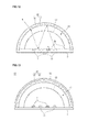
- the first and second light emitting devices 7 and 10 When viewed from the top, the first and second light emitting devices 7 and 10 may have rectangular shapes as shown in FIG. 5 , triangular shapes as shown in FIG. 6 , or hexagonal shapes as shown in FIG. 7 . Although not shown in the drawing, the first and second light emitting devices 7 and 10 may have polygonal shapes, such as circular shapes, elliptical shapes, lozenge shapes or square shapes, but the embodiment is not limited thereto.
- the first and second light emitting devices 7 and 10 may have the triangular shapes and may be alternately disposed.
- One side of the first light emitting device 7 may face one side of the second light emitting device 10, but the embodiment is not limited thereto.
- the first emitting device 7 when viewed from the top, the first emitting device 7 may have the hexagonal shape and the second light emitting devices 10 may be disposed such that one side of the second light emitting devices 10 may face sides of the hexagonal first emitting device 7, respectively.
- the second emitting device 10 when viewed from the top, may have the hexagonal shape and the first light emitting devices 7 may be disposed such that one side of the first light emitting devices 7 may face sides of the hexagonal second emitting device 10, respectively.
- a plurality of second light emitting devices 10 may be disposed to surround the hexagonal first emitting device 7, another hexagonal second light emitting device 10 may be disposed adjacent to the hexagonal first emitting device 7 and a plurality of first light emitting devices 7 may be disposed to surround the second light emitting device 10.
- the hexagonal first and second light emitting devices 7 and 10 may be alternately disposed
- a plurality of the second light emitting devices 10 may be disposed around the hexagonal first light emitting device 7 and a plurality of first light emitting devices 7 may be disposed around the hexagonal second light emitting device 10, but the embodiment is not limited thereto.
- the second and first light emitting devices 10 and 7 that surround the hexagonal first and second light emitting device 7 and 10, respectively, may have the rectangular shapes, but the embodiment is not limited thereto.
- the transparent layer 29 may be disposed on the substrate 3 to surround the first and second light emitting devices 7 and 10.
- the transparent layer 29 may be disposed between the first and second light emitting devices 7 and 10 and/or on the first and second light emitting devices 7 and 10.
- the transparent layer 29 is attached to the substrate 3 while surrounding the first and second light emitting devices 7 and 10.
- the first and second light emitting devices 7 and 10 are securely fixed to the substrate 3 so that the first and second light emitting devices 7 and 10 can be prevented from being detached from the substrate 3 by external impact and can be prevented from being contaminated or eroded by for instance, air of the medium layer 13.
- the transparent layer 29 may have the refractive index in the range of 1.4 to 2.0.
- the refractive index of the transparent layer 29 may be lower than the refractive index of the first and second light emitting devices by 0.1 to 1.5.
- the transparent layer 29 may be formed of a silicone-based resin or an epoxy-based resin having superior adhesive and thermal conductive properties, but the embodiment is not limited thereto.
- the silicon resin may have the refractive index of 1.45 to 1.60 and the epoxy-based resin may have the refractive index of 1.5, but the embodiment is not limited thereto.
- FIG. 2 is a view showing a traveling path of light when the medium layer is disposed on the first and second light emitting devices.
- the light generated from the first and second light emitting devices 7 and 10 may be totally reflected from a boundary surface 9 that is formed between the first and second light emitting devices 7 and 10 and the medium layer 13, so that the light is reflected into the interior of the first and second light emitting devices 7 and 10.
- the light travels from a first medium having the higher refractive index to a second medium having the lower refractive index.
- the light may not travel from the first medium to the second medium, but may be totally reflected into the first medium.
- the air may have the refractive index (n3) of 1.0003.
- the difference in refractive index between the first and second light emitting devices 7 and 10 and the medium layer 13 (n1-n3) may be in the range of 1.0997 to 1.8997.
- the light generated from the first and second light emitting devices 7 and 10 may not be output to the medium layer 13, so that the light extraction efficiency may be reduced, resulting the reduction of the light efficiency.
- the transparent layer 29 may be disposed between the first and second light emitting devices 7 and 10 the medium layer 13 so as to attenuate the difference in refractive index between the first and second light emitting devices 7 and 10 and the medium layer 13 (n1-n3).
- the refractive index (n2) of the transparent layer 29 may be lower than the refractive index (n1) of the first and second light emitting devices 7 and 10 and higher than the refractive index (n3) of the medium layer 13, but the embodiment is not limited thereto. That is, the transparent layer 29 may have the refractive index (n2) between the refractive index (n1) of the first and second light emitting devices 7 and 10 and the refractive index (n3) of the medium layer 13.
- the transparent layer 29 may have the refractive index (n2) in the range of 1.4 to 1.6, but the embodiment is not limited thereto.
- FIG. 3 is a view showing a traveling path of light when the transparent layer 29 is disposed between the medium layer 13 and the first and second light emitting devices 7 and 10 according to the first embodiment.
- the transparent layer 29 attenuates the difference in refractive index between the first and second light emitting devices 7 and 10 and the medium layer 13, the light generated from the first and second light emitting devices 7 and 10 can be readily incident into the medium layer 13 through the transparent layer 29.
- the difference in refractive index between the first and second light emitting devices 7 and 10 and the medium layer 13 (n1-n3) is lower than the difference in refractive index between the first and second light emitting devices 7 and 10 and the transparent layer 29 (n1-n2), the light generated from the first and second light emitting devices 7 and 10 can be readily incident into the transparent layer 29.
- the difference in refractive index between the first and second light emitting devices 7 and 10 and the medium layer 13 (n1-n3) is lower than the difference in refractive index between the transparent layer 29 and the medium layer (n2-n3), the light of the transparent layer 29 can be readily incident into the medium layer 13.
- the light generated from the first and second light emitting devices 7 and 10 can be readily incident into the medium layer 13 because the transparent layer 29 attenuates the difference in refractive index between the first and second light emitting devices 7 and 10 and the medium layer 13, so that the light extraction efficiency can be increased and the light efficiency can be improved.
- the transparent layer 29 When viewed from the top, the transparent layer 29 may have a circular shape or an elliptical shape, but the embodiment is not limited thereto.
- the transparent layer 29 When viewed from the side surface, the transparent layer 29 may have a hemispheric shape, but the embodiment is not limited thereto.
- the transparent layer 29 may have a hemispheric shape having a first radius R 1 .
- the first radius R 1 may be defined as a distance between the center of the transparent layer 29, that is, the center of the substrate 3 and the top surface of the transparent layer 29, but the embodiment is not limited thereto.
- the bottom surface of the transparent layer 29 may closely adhere to the first and second light emitting devices 7 and 10, but the embodiment is not limited thereto.
- the wavelength conversion layer 18 may be disposed on the medium layer 13.
- the wavelength conversion layer 18 is spaced apart from the first and second light emitting devices 7 and 10 and may be fixed or attached to the substrate 3.
- the wavelength conversion layer 18 may be attached to the substrate 3 by using an adhesive, but the embodiment is not limited thereto.
- the adhesive may be formed of a silicone-based resin or an epoxy-based resin having superior adhesive and thermal conductive properties, but the embodiment is not limited thereto.
- the wavelength conversion layer 18 may be prepared in the form of a hemispheric cap to prevent the light loss and to improve the light efficiency by suppressing difference in light path, but the embodiment is not limited thereto.
- the wavelength conversion layer 18 may be prepared in the form of a hemispheric cap having a second radius R 2 .
- the second radius R 2 may be defined as a distance between the center of the wavelength conversion layer 18, that is, the center of the substrate 3 and the top surface of the wavelength conversion layer 18, but the embodiment is not limited thereto.
- the wavelength conversion layer 18 has the second radius R 2 , the light generated from the first and second light emitting devices 7 and 10 disposed in the vicinity of the center the substrate 3 may have the same path to the wavelength conversion layer 18. That is, the same light path is formed between the first and second light emitting devices 7 and 10 and the wavelength conversion layer 18, so the light loss may not occur due to a difference between the light paths and the light efficiency may be improved.
- the shape of the wavelength conversion layer 18 according to the first embodiment may be variously modified depending on applications.
- the medium layer 13 and the wavelength conversion layer 18 may have the elliptical shape, but the embodiment is not limited thereto.
- each of the transparent layer 29, the medium layer 13 and the wavelength conversion layer 18 may have a long axis and a short axis.
- the first radius R 2 may be applied to the short axis of the transparent layer 29 and the second radius R 2 may be applied to the short axis of the wavelength conversion layer 18, but the embodiment is not limited thereto.
- the wavelength conversion layer 18 may convert the light having the first main wavelength band generated from the first light emitting device 7 or the light having the second main wavelength band generated from the second light emitting device 10 into the light having the third main wavelength band.
- the wavelength conversion layer 18 may include a transparent film 17 and a plurality of wavelength conversion particles 16 dispersed in the transparent film 17, but the embodiment is not limited thereto.
- the wavelength conversion particles 16 may be prepared as a single wavelength conversion particle or at least two wavelength conversion particles different from each other.
- the wavelength conversion particles 16 may include first and second wavelength conversion particles different from each other.
- the transparent film 17, for instance, may include one selected from the group consisting of a silicone-based resin, an epoxy-based resin, a polycarbonate-based resin and glass, which have superior light transmittance, thermal endurance and thermal conductivity, but the embodiment is not limited thereto.
- the silicone-based resin may have the refractive index of 1.45 to 1.60
- the epoxy-based resin may have the refractive index of 1.5
- the polycarbonate-based resin may have the refractive index of 1.59
- the glass may have the refractive index of 1.89, but the embodiment is not limited thereto.
- the wavelength conversion particles 16, for instance, may include phosphors formed of fluorescent materials, but the embodiment is not limited thereto.
- the fluorescent materials may include YAG-based materials or TAG-based materials, but the embodiment is not limited thereto.
- the YAG-based materials may include YAG:Ce and the TAG-based materials may include TAG:Tb.
- the fluorescent materials may include silicate-based materials.
- the silicate-based materials may include Sr 4- x Mg y Ba z Si 2 O 8 :Eu x 2 + (0 ⁇ x ⁇ 1, 0 ⁇ y ⁇ 1, 0 ⁇ z ⁇ 1) or Sr 3-x SiO 5 :Eu 2+x (0 ⁇ x ⁇ 1), but the embodiment is not limited thereto.
- At least one of the YAG-based materials, TAG-based materials and/or silicate-based materials may be dispersed in the transparent film 17 as a phosphor, but the embodiment is not limited thereto.
- the wavelength conversion particles 16 may be randomly dispersed in the transparent film 17, but the embodiment is not limited thereto.
- the wavelength conversion particles 16 may convert the light having the first main wavelength band generated from the first light emitting device 7 and/or the light having the second main wavelength band generated from the second light emitting device 10 into the light having the third main wavelength band, but the embodiment is not limited thereto.
- the light having the first main wavelength band generated from the first light emitting device 7 may pass through the transparent film 19 of the wavelength conversion layer 18 or may be converted into the light having the third main wavelength band by the wavelength conversion particles 16.
- the light having the second main wavelength band generated from the second light emitting device 10 may pass through the transparent film 19 of the wavelength conversion layer 18 or may be converted into the light having the third main wavelength band by the wavelength conversion particles 16.
- the light having the first main wavelength band, the light having the second main wavelength band, and the light having the third main wavelength band, which are output through the wavelength conversion layer 18, are mixed with each other to generate the light having the warm white.
- dispersion particles may be further dispersed in the transparent film 17 in addition to the wavelength conversion particles 16, but the embodiment is not limited thereto.
- the dispersion particles may include one selected from the group consisting of TiO 2 , Al 2 O 3 , BaCO 3 , BaSO 4 and SiO 2 , but the embodiment is not limited thereto.
- the light of the wavelength conversion layer 18 may be scattered or dispersed when the light is output from the wavelength conversion layer 18 so that the light extraction efficiency can be more improved.
- the wavelength conversion layer 18, in detail, the transparent film 17 allows the light of the medium layer 13 to be more easily incident into the wavelength conversion layer 18 while preventing the light of the wavelength conversion layer 18 from being incident again into the medium layer 13.
- the wavelength conversion layer 18 may have the refractive index higher than that of the medium layer 13.
- the wavelength conversion layer 18 may have the refractive index in the range of 1.4 to 2.0, but the embodiment is not limited thereto.
- the wavelength conversion layer 18 may have the refractive index equal to or different from that of the transparent layer 29.
- the wavelength conversion layer 18 may have the refractive index equal to or higher than that of the transparent layer 29, but the embodiment is not limited thereto.
- the wavelength conversion layer 18 may include the same material as a material of the transparent layer 29, but the embodiment is not limited thereto.
- the wavelength conversion layer 18 contacts the transparent layer 29 since the wavelength conversion layer 18 has the refractive index similar to that of the transparent layer 29, the light of the transparent layer 29 may be reflected from the wavelength conversion layer 18, other than incident into the wavelength conversion layer 18, so that the light may be incident again into the transparent layer 29.
- the wavelength conversion layer 18 is spaced apart from the transparent layer 29 while interposing the medium layer 13 therebetween, the light incident into the medium layer from the transparent layer 29 may be readily incident into the wavelength conversion layer 18 having the refractive index significantly higher than the refractive index of the medium layer 13. Due to the above structure, the light can be incident into the wavelength conversion layer 18 with higher probability, so that the wavelength conversion efficiency in the wavelength conversion layer 18 can be maximized.
- the medium layer 13 may be disposed between the transparent layer 29 and the wavelength conversion layer 18.
- the medium layer 13 has the refractive index lower than the refractive index of the transparent layer 29 or the wavelength conversion layer 18, but the embodiment is not limited thereto.
- the medium layer 13 has the refractive index in the range of 1 to 1.3, but the embodiment is not limited thereto.
- the medium layer 13 may include one selected from the group consisting of a vacuum medium, air and liquid carbon dioxide, but the embodiment is not limited thereto.
- the vacuum medium may have the refractive index of 1.00
- the air may have the refractive index of 1.0003
- the liquid carbon dioxide may have the refractive index of 1.2.
- the refractive index of the medium layer 13 is lower than that of the wavelength conversion layer 18, the light of the medium layer 13 may be easily incident into the wavelength conversion layer 18, but the light of the wavelength conversion layer 18 may be totally reflected from the boundary surface between the wavelength conversion layer 18 and the medium layer 13, other than incident into the medium layer 13, so that the light of the wavelength conversion layer 18 may be incident again into the wavelength conversion layer 18.
- the medium layer 13 since the medium layer 13 is disposed under the wavelength conversion layer 18, the light of the medium layer 13 may be more easily incident into the wavelength conversion layer 18 while preventing the light of the wavelength conversion layer 18 from being incident into the medium layer 13. Thus, a greater amount of light may exist in the wavelength conversion layer 18 so that the wavelength conversion efficiency in the wavelength conversion layer 18 may be maximized.
- the medium layer 13 may have a hemispheric shape when viewed from the side surface, but the embodiment is not limited thereto.
- the wavelength conversion layer 18 is spaced apart from the first and second light emitting devices 7 and 10 by the medium layer 13, heat generated from the first and second light emitting devices 7 and 10 may not be transferred to the wavelength conversion layer 18, so the wavelength conversion layer 18 may not be damaged by heat.
- the degradation of the wavelength conversion characteristic of the wavelength conversion particles 16 dispersed in the wavelength conversion layer 18, which may be caused by the heat generated from the first and second light emitting devices 7 and 10, can be prevented.
- wavelength conversion layer 18 Since the wavelength conversion layer 18 is fixed to the substrate 3, heat of the wavelength conversion layer 18 can be readily dissipated to the outside through the substrate 3 even if the heat is transferred to the wavelength conversion layer 18 through air.
- the top surface of the wavelength conversion layer 18 may be formed with a roughness structure or a texture to improve the light extraction efficiency, but the embodiment is not limited thereto.
- the transparent layer 29 may have the first radius R 1 and the wavelength conversion layer 18 may the second radius R 2 .
- the medium layer 13 may have a width D corresponding to a distance between the second radius R 2 of the wavelength conversion layer 18 and the first radius R 1 of the transparent layer 29.
- the width D may be in the range of 0.5 mm to 50 mm, but the embodiment is not limited thereto.
- the width D may be defined as a distance between the bottom surface of the wavelength conversion layer 18 and the top surface of the transparent layer 29.
- the width D may be uniformly formed over the whole area between the bottom surface of the wavelength conversion layer 18 and the top surface of the transparent layer 29, but the embodiment is not limited thereto.
- the width D is uniformly formed over the whole area between the bottom surface of the wavelength conversion layer 18 and the top surface of the transparent layer 29, the light path from the top surface of the transparent layer 29 to the bottom surface of the wavelength conversion layer 18 is uniform, so the light loss can be prevented and the light efficiency can be improved.
- FIG. 8 is a sectional view showing a light emitting apparatus according to the second embodiment.
- the second embodiment is substantially identical to the first embodiment except for a plurality of holes 23 formed in the wavelength conversion layer 18.
- the description of the first embodiment may be adopted in the second embodiment even if it is omitted in the second embodiment and the contents omitted in the second embodiment may be easily comprehended by referring to the first embodiment.
- the light emitting apparatus 1A may include a substrate 3, a plurality of first and second light emitting devices 7 and 10, a transparent layer 29, a medium layer 13 and a wavelength conversion layer 18.
- the wavelength conversion layer 18 may be prepared in the form of a hemispheric cap, but the embodiment is not limited thereto.
- the wavelength conversion layer 18 may include a plurality of holes 23 that are spaced apart from each other.
- the holes 23 may be formed through the bottom surface and the top surface of the wavelength conversion layer 18.
- the holes 23 may have an area corresponding to 10% to 30% with respect to the whole area of the wavelength conversion layer 18, but the embodiment is not limited thereto.
- the wavelength conversion area is reduced in the wavelength conversion layer 18 so that the wavelength conversion efficiency may be lowered.
- the holes 23 may have the same diameter or different diameters, but the embodiment is not limited thereto.
- the holes 23 may be regularly or randomly spaced apart from each other, but the embodiment is not limited thereto.
- the light that reaches the holes 23 of the wavelength conversion layer 18 from the first and second light emitting devices 7 and 10 by way of the medium layer 13 can be output to the outside through the holes 23.
- the holes 23 are formed in the wavelength conversion layer 18 so that the light extraction efficiency can be improved.
- the holes 23 may have circular shapes when viewed from the top, but the embodiment is not limited thereto. That is, the holes 23 may have triangular shapes, rectangular shapes, star shapes or lozenge shapes.
- the holes 23 may have the same size or same diameter as shown in FIG. 9 , or the holes 23 may have different sizes or different diameters.
- the holes 23 formed in the center region of the wavelength conversion layer 18 may have relatively small sizes or diameters and the holes 23 formed in the peripheral region of the wavelength conversion layer 18 may have relatively large sizes or diameters.
- the sizes or diameters of the holes 23 may be gradually enlarged linearly or nonlinearly from the center region of the wavelength conversion layer 18 to the peripheral region of the wavelength conversion layer 18.
- the holes 23 formed in the peripheral region of the wavelength conversion layer 18, in which a smaller amount of light is output may have the sizes larger than the sizes of the holes 23 formed in the center region of the wavelength conversion layer 18, in which a greater amount of light is output, in such a manner that a greater amount of light can be extracted in the peripheral region of the wavelength conversion layer 18. In this case, the light can be uniformly output through the whole area of the wavelength conversion layer 18 so that the uniform light brightness can be ensured.
- the holes 23 may be formed only in the peripheral region of the wavelength conversion layer 18 without being formed in the center region of the wavelength conversion layer 18.
- the transparent layer formed on a resin material can be formed instead of the medium layer. That is, the transparent layer may be formed on the substrate 3 to surround the first and second light emitting devices 7 and 10 and the wavelength conversion layer 18 may be disposed on the transparent layer while adhering to the transparent layer.
- the transparent layer may include a silicone-based resin or an epoxy-based resin, but the embodiment is not limited thereto.
- the transparent layer may have the refractive index lower than the refractive index of the transparent layer 29 and the wavelength conversion layer 18. For instance, the transparent layer that substitutes for the medium layer 13 may have the refractive index in the range of 1.1 to 1.3.
- FIG. 10 is a sectional view showing a light emitting apparatus according to the third embodiment.
- the third embodiment is substantially identical to the first embodiment except for a plurality of grooves 26 formed in the wavelength conversion layer 18.
- the description of the first embodiment may be adopted in the third embodiment even if it is omitted in the third embodiment and the contents omitted in the third embodiment may be easily comprehended by referring to the first embodiment.
- the light emitting apparatus 1B may include a substrate 3, a plurality of first and second light emitting devices 7 and 10, a transparent layer 29, a medium layer 13 and a wavelength conversion layer 18.
- the wavelength conversion layer 18 may be prepared in the form of a hemispheric cap, but the embodiment is not limited thereto.
- the wavelength conversion layer 18 may include a plurality of grooves 26 that are spaced apart from each other.
- the grooves 26 may have concave shapes, which are concaved inward, that is, concaved downward from the top surface of the wavelength conversion layer 18.
- a transparent film 17 having a predetermined thickness may be formed between the bottom surface of the groove 26 and the bottom surface of the wavelength conversion layer 18.
- a first thickness between the bottom surface of the groove 26 and the bottom surface of the wavelength conversion layer 18 may be smaller than a second thickness between the top surface and the bottom surface of the wavelength conversion layer 18.
- the grooves 26 may have concave shapes, which are concaved inward, that is, concaved upward from the bottom surface of the wavelength conversion layer 18.
- the grooves 26 may have an area corresponding to 10% to 30% based on the whole area of the wavelength conversion layer 18, but the embodiment is not limited thereto.
- the wavelength conversion area is reduced in the wavelength conversion layer 18 so that the wavelength conversion efficiency may be lowered.
- the grooves 26 are formed in the wavelength conversion layer 18 so that the light extraction efficiency can be improved.
- the grooves 26 may have circular shapes when viewed from the top, but the embodiment is not limited thereto. That is, the grooves 26 may have triangular shapes, rectangular shapes, star shapes or lozenge shapes.
- the grooves 26 may be concaved down from the top surface of the wavelength conversion layer 18.
- the grooves 26 may have the same size or same diameter or may have different sizes or different diameters.
- the grooves 26 formed in the center region of the wavelength conversion layer 18 may have relatively small sizes or diameters and the grooves 26 formed in the peripheral region of the wavelength conversion layer 18 may have relatively large sizes or diameters.
- the sizes or diameters of the grooves 26 may be gradually enlarged linearly or nonlinearly from the center region of the wavelength conversion layer 18 to the peripheral region of the wavelength conversion layer 18.
- the grooves 26 formed in the peripheral region of the wavelength conversion layer 18, in which a smaller amount of light is output may have the sizes larger than the sizes of the grooves 26 formed in the center region of the wavelength conversion layer 18, in which a greater amount of light is output, in such a manner that a greater amount of light can be extracted in the peripheral region of the wavelength conversion layer 18. In this case, the light can be uniformly output through the whole area of the wavelength conversion layer 18 so that the uniform light brightness can be ensured.
- the grooves 26 may be formed only in the peripheral region of the wavelength conversion layer 18 without being formed in the center region of the wavelength conversion layer 18.
- grooves 26 may have the same depth or different depths.
- the depth of the grooves 26 in the peripheral region of the wavelength conversion layer 18 may be greater than the depth of the grooves 26 in the center region of the wavelength conversion layer 18.
- the depth of the grooves 26 in the center region of the wavelength conversion layer 18 may be greater than the depth of the grooves 26 in the peripheral region of the wavelength conversion layer 18.
- protrusions may be formed in place of the grooves 26, but the embodiment is not limited thereto.
- the protrusions may protrude upward from the top surface of the wavelength conversion layer 18 or may protrude downward from the bottom surface of the wavelength conversion layer 18.
- the shape, size and interval of the protrusions are similar to those of the grooves 26.
- FIG. 11 is a sectional view showing a light emitting apparatus according to the fourth embodiment.
- the fourth embodiment is substantially identical to the first embodiment except for a diffusion layer 32 disposed between the first and second light emitting devices 7 and 10.
- the description of the first embodiment may be adopted in the fourth embodiment even if it is omitted in the fourth embodiment and the contents omitted in the fourth embodiment may be easily comprehended by referring to the first embodiment.
- the light emitting apparatus 1C may include a substrate 3, a plurality of first and second light emitting devices 7 and 10, a transparent layer 29, a medium layer 13 and a wavelength conversion layer 18.
- a diffusion layer 32 may be disposed between the transparent layer 29 and the substrate 3. That is, the diffusion layer 32 may be disposed between the bottom surface of the transparent layer 29 and the top surface of the substrate 3.
- the bottom surface of the diffusion layer 32 can contact the top surface of the substrate 3 and the top surface of the diffusion layer 32 can contact the bottom surface of the transparent layer 29, but the embodiment is not limited thereto.
- the diffusion layer 32 can contact side surfaces of the first and second light emitting devices 7 and 10.
- the diffusion layer 32 may be disposed on a region (hereinafter, referred to as a second region) of the substrate 3 except for a first region of the substrate 3 where the first and second light emitting devices 7 and 10 are attached. That is, the diffusion layer 32 may be disposed on the second region of the substrate 3.
- a side surface of the diffusion layer 32 can contact an inner surface of the wavelength conversion layer 18 that is fixed to the substrate 3.
- the top surface of the diffusion layer 32 may be disposed on the same plane with the top surface of the first and second light emitting devices 7 and 10 or higher/lower than the top surface of the first and second light emitting devices 7 and 10, but the embodiment is not limited thereto. Thus, the whole area of the side surfaces of the first and second light emitting devices 7 and 10 can contact the diffusion layer 32.
- the top surface of the diffusion layer 32 may be located at a half of the side surface of the first and second light emitting devices 7 and 10, but the embodiment is not limited thereto.
- the diffusion layer 32 may include a transparent film and a plurality of dispersion particles dispersed in the transparent film, but the embodiment is not limited thereto.
- the transparent film may include one selected from the group consisting of a silicone-based resin, a white epoxy-based resin, and PTFE (polytetrafluoroethylene), which have superior electric insulating property, thermal endurance and thermal conductivity, but the embodiment is not limited thereto.
- a silicone-based resin a white epoxy-based resin
- PTFE polytetrafluoroethylene
- the dispersion particles may include one selected from the group consisting of TiO 2 , Al 2 O 3 , BaCO 3 , BaSO 4 and SiO 2 , but the embodiment is not limited thereto.
- the dispersion particles may have superior dispersion property with respect to the light having the first main wavelength band (about 400 nm to about 500 nm) generated from the first light emitting device 7.
- the light having the first main wavelength band (about 400 nm to about 500 nm) reaches the second light emitting device 10 that generates the light having the second main wavelength band (about 600 nm to about 670 nm)
- the light having the first main wavelength band is absorbed in the second light emitting device 10, so the quantity of the light having the first main wavelength band may be reduced.
- the diffusion layer 32 closely adheres to the side surface of the first light emitting device 7.
- the light having the first main wavelength band, which travels toward the side surface of the first light emitting device 7 may be scattered, dispersed or reflected by the diffusion layer 32 so that the light does not reach the second light emitting device 10. Accordingly, the quantity of the light having the first main wavelength band generated from the first light emitting device 7 may not be reduced.
- the light having the first main wavelength band generated from the first light emitting device 7 or the light having the second main wavelength band generated from the second light emitting device 10 may be output to the outside through the wavelength conversion layer 18 by way of the medium layer 13 or may be reflected from the wavelength conversion layer 18 so that the light may travel in the downward direction by way the medium layer 13.
- the light traveling in the downward direction may be again scattered, dispersed or reflected by the diffusion layer 32 so that the light may travel in the upward direction.
- the light which is generated from the first and second light emitting devices 7 and 10 and reflected by the wavelength conversion layer 18 to travel in the downward direction, may be again scattered, dispersed or reflected in the upward direction by the diffusion layer 32, so that the light loss caused by the absorption of light in the substrate 3 may be minimized, thereby improving the light efficiency.
- FIG. 13 is a sectional view showing a light emitting apparatus according to the fifth embodiment.
- the fifth embodiment is substantially identical to the first embodiment except for a transparent layer 20 disposed on a wavelength conversion layer 18.
- the description of the first embodiment may be adopted in the fifth embodiment even if it is omitted in the fifth embodiment and the contents omitted in the fifth embodiment may be easily comprehended by referring to the first embodiment.
- the light emitting apparatus ID may include a substrate 3, a plurality of first and second light emitting devices 7 and 10, a transparent layer 29, a medium layer 13 and the wavelength conversion layer 18.
- Another transparent layer 20 may be further disposed on the wavelength conversion layer 18.
- the transparent layer 29 will be referred to as a first transparent layer and the transparent layer 20 will be referred to as a second transparent layer.
- the second transparent layer 20 may have the refractive index lower than the refractive index of the wavelength conversion layer 18.
- the second transparent layer 20, for instance, may include a silicone-based resin or an epoxy-based resin having superior light transmittance, thermal endurance and thermal conductivity, but the embodiment is not limited thereto.
- the silicone-based resin may have the refractive index of 1.42 to 1.60 and the epoxy-based resin may have the refractive index of 1.5, but the embodiment is not limited thereto.
- the wavelength conversion layer 18 may be formed of glass having the refractive index of 1.89, and the second transparent layer 20 may be formed of the epoxy-based resin having the refractive index of 1.5.
- the light of the wavelength conversion layer 18 may not be readily output to the outside due to the great difference in refractive index between the wavelength conversion layer 18 and the atmosphere.
- the second transparent layer 20 having the refractive index between the refractive index of the wavelength conversion layer 18 and the refractive index of the atmosphere may be provided to attenuate the great difference in refractive index between the wavelength conversion layer 18 and the atmosphere. That is, the second transparent layer 20 may have the refractive index lower than the refractive index of the wavelength conversion layer 18 and higher than the refractive index of the atmosphere. Thus, the light of the wavelength conversion layer 18 may be readily output to the outside by way of the second transparent layer 20.
- the second transparent layer 20 may include a plurality of transparent films to maximally attenuate the difference in refractive index.
- the transparent films may have different indexes, which are linearly or nonlinearly reduced from the wavelength conversion layer 18 to the outside.
- FIG. 14 is a sectional view showing a light emitting apparatus according to the sixth embodiment.
- the light emitting apparatus 1E may include a substrate 3, a plurality of first and second light emitting packages 40 and 50, and a transparent layer 34.
- the substrate 3 has been described in detail in the first embodiment, so the detailed description thereof will be omitted.
- the substrate 3 may be easily comprehended from the description of the first embodiment.
- the transparent layer 34 may be disposed on a wavelength conversion layer 49 of the first light emitting package 50 shown in FIG. 15 .
- the transparent layer 34 may have the refractive index lower than the refractive index of the wavelength conversion layer 49.
- the transparent layer 34 may be formed of a silicone-based resin or an epoxy-based resin having superior adhesive and thermal conductive properties, but the embodiment is not limited thereto.
- the first and second light emitting packages 40 and 50 may be attached onto the substrate 3 by using an adhesive.
- the first light emitting package 40 may serve as a first light source for generating light having a first main wavelength band and light having a third main wavelength band and the second light emitting package 50 may serve as a second light source for generating light having a second main wavelength band, but the embodiment is not limited thereto.
- the first light emitting package 40 may include a first light emitting device for generating the light having the first main wavelength band and a wavelength conversion layer for converting the light having the first main wavelength band into the light having the third main wavelength band.
- the second light emitting package 50 may include a second light emitting device for generating the light having the second main wavelength band
- the first main wavelength band may be in the range of about 400 nm to about 500 nm
- the second main wavelength band may be in the range of about 600 nm to about 670 nm
- the third main wavelength band may be in the range of about 500 nm to about 600 nm, but the embodiment is not limited thereto.
- the first main wavelength band may have a peak of 450 nm
- the second main wavelength band may have a peak of 615 nm
- the third main wavelength band may have a peak in the range of 550 nm to 560 nm, but the embodiment is not limited thereto.
- the warm white light may be generated by mixing the light having the first main wavelength band and the light having the third main wavelength band, which are generated from the first light emitting package 40, with the light having the second main wavelength band generated from the second light emitting package 50, but the embodiment is not limited thereto.
- the first light emitting package 40 as shown in FIGS. 15 to 17 , may be modified to have various structures.
- the light emitting package 40 includes a body 42 as well as a first light emitting device, a medium layer, a transparent layer and a wavelength conversion layer, which are substantially identical to the first light emitting device 7, the medium layer 13, the transparent layer 29 and the wavelength conversion layer 18 according to the first embodiment, so the description thereof will be omitted.
- the first light emitting package 40 may include first and second electrode lines formed on the body 42 to electrically connect the first light emitting package 40 to the first light emitting device 44.
- a reflective layer may be coated on the first and second electrode lines and/or the body to improve the light efficiency by reflecting the light generated from the first light emitting device 44.
- the first light emitting package 40 may include the body 42, the first light emitting device 44, the transparent layer 71, the medium layer 46 and the wavelength conversion layer 49.
- the body 42 may serve as a substrate to support the first light emitting device 44.
- the body 42 may include a silicon material, a synthetic resin material or a metallic material, but the embodiment is not limited thereto.
- a cavity may be formed in the top surface of the body 42 and the first light emitting device 44 may be disposed on a bottom surface of the body 42.
- the first light emitting device 44 may be attached to the first and second electrode lines of the body 42 through the flip chip bonding or die bonding, but the embodiment is not limited thereto.
- the first light emitting device 44 may be formed of group II-VI semiconductor materials or group III-V compound semiconductor materials to generate the light having the first main wavelength band.
- the transparent layer 71 is attached onto the body 42 while surrounding the first light emitting device 44.
- the first light emitting device 44 is securely fixed to the body 44 so that the first light emitting device 44 can be prevented from being detached from the body by external impact and can be prevented from being contaminated or eroded by air of the medium layer 46.
- the transparent layer 71 may have the refractive index between the refractive indexes of the first light emitting device 44 and the medium layer 46. That is, the transparent layer 71 may have the refractive index lower than the refractive index of the first light emitting device 44 and higher than the refractive index of the medium layer 46.
- the transparent layer 71 may attenuate the difference in refractive index between the first light emitting device 44 and the medium layer 46, so the light of the first light emitting device 44 can be more readily incident into the medium layer 46.
- the wavelength conversion layer 49 may be spaced apart from the transparent layer 71 while interposing the medium layer 46 therebetween.
- the wavelength conversion layer 49 may have the refractive index higher than that of the medium layer 46. Thus, the light travelled to the medium layer 46 from the first light emitting device 44 can be incident into the wavelength conversion layer 49 without light loss, so that the wavelength conversion efficiency of the wavelength conversion layer 49 can be maximized.
- the wavelength conversion layer 49 may include a transparent film 48 and a plurality of wavelength conversion particles 47 dispersed in the transparent film 48.
- the light generated from the first light emitting device 44 may be converted into the light having the third main wavelength band by the wavelength conversion particles 47.
- the light generated from the first light emitting device 44 may be output to the outside through spaces defined between the wavelength conversion particles 47 and the transparent film 48.
- the first light emitting device 44 can output the light having the first main wavelength band and the light having the third main wavelength band.
- the greenish light may be seen to the naked eyes of the user, but the embodiment is not limited thereto.
- the medium layer 46 may have a width D defined as a difference between the second radius r 2 of the wavelength conversion layer 49 and the first radius r 1 of the transparent layer 71.
- the medium layer 46 may be formed to have a width d defined between the second radius r 2 of the wavelength conversion layer 49 and the first radius r 1 of the transparent layer 71.
- the width d may be uniformly formed over the whole area between the wavelength conversion layer 49 and the transparent layer 71, but the embodiment is not limited thereto.
- a first light emitting package 40A may include a body 42, a first light emitting device 44, a transparent layer 71, a medium layer 46 and a wavelength conversion layer 49.
- the wavelength conversion layer 49 may include a plurality of holes 65 spaced apart from each other.
- the holes 65 may be formed through the bottom surface and the top surface of the wavelength conversion layer 49.
- the holes 65 may have an area corresponding to 10% to 30% based on the whole area of the wavelength conversion layer 49.
- the first light emitting package 40A shown in FIG. 16 may improve the light extraction efficiency by forming the holes 65 in the wavelength conversion layer 49.
- the holes 65 may have circular shapes, triangular shapes, rectangular shapes, star shapes or lozenge shapes when viewed from the top.
- the holes 65 may have the same size or diameter or different sizes or diameters.
- the holes 65 formed in the center region of the wavelength conversion layer 49 may have relatively small sizes or diameters and the holes 65 formed in the peripheral region of the wavelength conversion layer 49 may have relatively large sizes or diameters.
- the sizes or diameters of the holes 65 may be gradually enlarged linearly or nonlinearly from the center region of the wavelength conversion layer 49 to the peripheral region of the wavelength conversion layer 49.
- the holes 65 may be formed only in the peripheral region of the wavelength conversion layer 49 without being formed in the center region of the wavelength conversion layer 49.
- a first light emitting package 40B may include a body 42, a first light emitting device 44, a transparent layer 71, a medium layer 46 and a wavelength conversion layer 49.
- the wavelength conversion layer 49 may include a plurality of grooves 67 instead of the holes 65 shown in FIG. 16 .
- the grooves 67 may be spaced apart from each other in the top surface of the wavelength conversion layer 49.
- the grooves 67 may have an area corresponding to 10% to 30% based on the whole area of the wavelength conversion layer 49.
- the grooves 67 have depths that may vary depending on positions in the wavelength conversion layer 49. For instance, the depth of the groove 67 in the peripheral region of the wavelength conversion layer 49 may be greater than the depth of the groove 67 in the center region of the wavelength conversion layer 49. Otherwise, the depth of the groove 67 in the center region of the wavelength conversion layer 49 may be greater than the depth of the groove 67 in the peripheral region of the wavelength conversion layer 49.
- the grooves 67 have sizes or diameters that may vary depending on positions in the wavelength conversion layer 49. For instance, the sizes or diameters of the groove 67 in the peripheral region of the wavelength conversion layer 49 may be greater than the sizes or diameters of the groove 67 in the center region of the wavelength conversion layer 49. Otherwise, the sizes or diameters of the groove 67 in the center region of the wavelength conversion layer 49 may be greater than the sizes or diameters of the groove 67 in the peripheral region of the wavelength conversion layer 49.
- FIG. 18 is a sectional view showing a second light emitting package of FIG. 14 .
- the second light emitting package 50 may include a body 52, a second light emitting device 54, and a transparent layer 56.
- the body 52 may serve as a substrate to support the second light emitting device 54.
- the body 52 may include a silicon material, a synthetic resin material or a metallic material, but the embodiment is not limited thereto.
- a cavity may be formed in the top surface of the body 52 and the second light emitting device 54 may be disposed on a bottom surface of the body 52.
- the second light emitting device 54 may be formed of group II-VI semiconductor materials or group III-V compound semiconductor materials to generate the light having the second main wavelength band.
- the transparent layer 56 may include an epoxy-based resin or a silicon resin having superior transmittance and insulating properties, but the embodiment is not limited thereto.
- the transparent layer 56 When viewed from the side surface, the transparent layer 56 may have a hemispherical shape, but the embodiment is not limited thereto.
- a recess may be formed at the center region of the top surface of the transparent layer 56, but the embodiment is not limited thereto.
- the top surface of the transparent layer 56 may be formed with a roughness structure or a texture to improve the light extraction efficiency, but the embodiment is not limited thereto.
- FIGS. 19 to 21 are views showing an arrangement of the first and second light emitting packages.
- the arrangement of the first and second light emitting packages 40 and 50 shown in FIGS. 19 to 21 are substantially identical to the arrangement of the first and second light emitting devices 7 and 10 shown in FIGS. 2 to 4 .
- the arrangement of the first and second light emitting packages 40 and 50 shown in FIGS. 19 to 21 can be readily comprehended from the arrangement of the first and second light emitting devices 7 and 10 shown in FIGS. 2 to 4 , so the detailed description thereof will be omitted.
- FIG. 22 is a sectional view showing a light emitting apparatus according to the seventh embodiment.
- the seventh embodiment is substantially identical to the sixth embodiment shown in FIG. 14 except for a light emitting package 80.
- the warm white light is generated by the first and second light emitting packages 40 and 50
- the warm white light is generated by the single light emitting package 80 in the seventh embodiment.
- the light emitting apparatus 1F may include a substrate 3, a plurality of light emitting packages 80 and a transparent layer 34.
- the light emitting packages 80 may be attached to the substrate 3 while being spaced apart from each other.
- the transparent layer 34 may be disposed on the substrate 3 to surround the light emitting packages 80.
- the transparent layer 34 may be disposed on a wavelength conversion layer 89 of the light emitting package 80 shown in FIG. 23 as well as on the substrate 3.
- the transparent layer 34 may have the refractive index lower than the wavelength conversion layer 89.
- the transparent layer 34 may be formed of a silicone-based resin or an epoxy-based resin having superior adhesive and thermal conductive properties, but the embodiment is not limited thereto.
- the transparent layer 34 may be directly formed on the substrate 3 through the forming process.
- the transparent layer 34 may be attached onto the substrate after processing the transparent layer 34 to have a hemispheric structure, but the embodiment is not limited thereto.
- the bottom surface of the transparent layer 34 may be formed with a recess corresponding to the shape of the light emitting package 80.
- the light emitting package 80 may generate the warm white light by mixing the light having the first main wavelength band, the light having the second main wavelength band and the light having the third main wavelength band.
- the first main wavelength band may be in the range of about 400 nm to about 500 nm
- the second main wavelength band may be in the range of about 600 nm to about 670 nm
- the third main wavelength band may be in the range of about 500 nm to about 600 nm, but the embodiment is not limited thereto.
- the first main wavelength band may have a peak of 450 nm
- the second main wavelength band may have a peak of 615 nm
- the third main wavelength band may have a peak in the range of 550 nm to 560 nm, but the embodiment is not limited thereto.
- the light emitting apparatus 1F according to the seventh embodiment can generate the warm white light by mixing the light having the first main wavelength band, the light having the second main wavelength band and the light having the third main wavelength band, but the embodiment is not limited thereto.
- the light emitting package 80 includes a body 82 as well as a first light emitting device, a medium layer, a transparent layer and a wavelength conversion layer, which are substantially identical to the first light emitting device 7, the medium layer 13, the transparent layer 29 and the wavelength conversion layer 18 according to the first embodiment, so the description thereof will be omitted.
- the light emitting package 80 may further include first and second electrode lines electrically connected to the first and second light emitting devices 84 and 85, respectively.
- a reflective layer may be coated on the first and second electrode lines or the body 82 to improve the light efficiency by reflecting the light generated from the first light emitting device 84 or the second light emitting device 85.
- the first and second electrode lines may serve as a heat dissipation member to discharge heat generated from the first light emitting device 84 or the second light emitting device 85 to the outside.
- the light emitting package 80 may include the body 82, a plurality of first and second light emitting devices 84 and 85, the transparent layer 99, the medium layer 86 and the wavelength conversion layer 89.
- the body 82 may have a flat top surface or a cavity may be formed in the top surface of the body 82.
- the first and second light emitting devices 84 and 85 may be attached onto the flat top surface of the body 82 or the bottom surface of the cavity.
- the first and second light emitting devices 84 and 85 may be attached onto the body 82 while being spaced apart from each other. In addition, the first and second light emitting devices 84 and 85 may be attached onto the electrode lines of the body 82 through the flip chip bonding or die bonding.
- the first light emitting device 84 may serve as a first light source for generating light having a first main wavelength band and the second light emitting device 85 may serve as a second light source for generating light having a second main wavelength band, but the embodiment is not limited thereto.
- the transparent layer 99 is attached onto the body 82 while surrounding the first and second light emitting devices 84 and 85.
- the first and second light emitting devices 84 and 85 can be more securely fixed to the body 82 so that the first and second light emitting devices 84 and 85 can be prevented from being detached from the body 82 by external impact and can be prevented from being contaminated or eroded by air of the medium layer 86.
- the transparent layer 99 may have the refractive index between the refractive indexes of the first and second light emitting devices 84 and 85 and the medium layer 46. That is, the transparent layer 99 may have the refractive index lower than the refractive index of the first and second light emitting devices 84 and 85 and higher than the refractive index of the medium layer 86.
- the transparent layer 99 may attenuate the difference in refractive index between the first and second light emitting devices 84 and 85 and the medium layer 86, so the light of the first and second light emitting devices 84 and 85 can be more readily incident into the medium layer 86.
- the wavelength conversion layer 89 may be spaced apart from the transparent layer 99 while interposing the medium layer 86 therebetween.
- the wavelength conversion layer 89 may have the refractive index higher than that of the medium layer 86.
- the light travelled to the medium layer 86 from the first and second light emitting devices 84 and 85 can be incident into the wavelength conversion layer 89 without light loss, so that the wavelength conversion efficiency of the wavelength conversion layer 89 can be maximized.
- the wavelength conversion layer 89 may include a transparent film 88 and a plurality of wavelength conversion particles 87 dispersed in the transparent film 88.
- the light having the first main wavelength band generated from the first light emitting device 84 or the light having the second main wavelength band generated from the second light emitting device 85 may be converted into the light having the third main wavelength band by the wavelength conversion particles 87.
- the wavelength conversion particles 87 may include phosphors, but the embodiment is not limited thereto.
- the medium layer 86 may have a width d defined between the second radius r 2 of the wavelength conversion layer 89 and the first radius r 1 of the transparent layer 99.
- the width d may correspond to a distance between the top surface of the transparent layer 99 and the bottom surface of the wavelength conversion layer 89.
- a light emitting package 80A may include the body 82, the first and second light emitting devices 84 and 85, the transparent layer 99, the medium layer 86 and the wavelength conversion layer 89.
- the wavelength conversion layer 89 may include a plurality of holes 95 spaced apart from each other.
- the holes 95 may be formed through the bottom surface and the top surface of the wavelength conversion layer 89.
- the holes 95 may have an area corresponding to 10% to 30% based on the whole area of the wavelength conversion layer 89.
- the light emitting package 80A shown in FIG. 24 may improve the light extraction efficiency by forming the holes 95 in the wavelength conversion layer 89.
- the holes 95 may have circular shapes, triangular shapes, rectangular shapes, star shapes or lozenge shapes when viewed from the top.
- the holes 95 may have the same size or diameter or different sizes or diameters.
- the holes 95 formed in the center region of the wavelength conversion layer 89 may have relatively small sizes or diameters and the holes 95 formed in the peripheral region of the wavelength conversion layer 89 may have relatively large sizes or diameters.
- the sizes or diameters of the holes 95 may be gradually enlarged linearly or nonlinearly from the center region of the wavelength conversion layer 89 to the peripheral region of the wavelength conversion layer 89.
- the holes 95 may be formed only in the peripheral region of the wavelength conversion layer 89 without being formed in the center region of the wavelength conversion layer 89.
- a light emitting package 80B may include a body 82, first and second light emitting devices 84 and 85, a transparent layer 99, a medium layer 86 and a wavelength conversion layer 89.
- the wavelength conversion layer 89 may include a plurality of grooves 97 instead of the holes 95 shown in FIG. 24 .
- the grooves 97 may be spaced apart from each other in the top surface of the wavelength conversion layer 89.
- the grooves 97 may have an area corresponding to 10% to 30% based on the whole area of the wavelength conversion layer 89.
- the grooves 97 have depths that may vary depending on positions in the wavelength conversion layer 89. For instance, the depth of the groove 97 in the peripheral region of the wavelength conversion layer 89 may be greater than the depth of the groove 97 in the center region of the wavelength conversion layer 89. Otherwise, the depth of the groove 97 in the center region of the wavelength conversion layer 89 may be greater than the depth of the groove 97 in the peripheral region of the wavelength conversion layer 89.
- the grooves 97 have sizes or diameters that may vary depending on positions in the wavelength conversion layer 89. For instance, the sizes or diameters of the groove 97 in the peripheral region of the wavelength conversion layer 89 may be greater than the sizes or diameters of the groove 97 in the center region of the wavelength conversion layer 89. Otherwise, the sizes or diameters of the groove 97 in the center region of the wavelength conversion layer 89 may be greater than the sizes or diameters of the groove 97 in the peripheral region of the wavelength conversion layer 89.
- a light emitting package 80C may include a body 82, first and second light emitting devices 84 and 85, a transparent layer 99, a medium layer 86 and a wavelength conversion layer 89.
- a diffusion layer 83 may be disposed between the transparent layer 99 and the body 82.
- the diffusion layer 83 can contact side surfaces of the first and second light emitting devices 84 and 85.
- the diffusion layer 83 may be disposed on a region (hereinafter, referred to as a second region) of the body 82 except for a first region of the body 82 where the first and second light emitting devices 84 and 85 are attached.
- a side surface of the diffusion layer 83 can contact an inner area of the wavelength conversion layer 89 fixed to the body 82.
- the top surface of the diffusion layer 83 may be disposed on the same plane with the top surface of the first and second light emitting devices 84 and 85 or higher/lower than the top surface of the first and second light emitting devices 84 and 85, but the embodiment is not limited thereto. Thus, the whole area of the side surfaces of the first and second light emitting devices 84 and 85 can contact the diffusion layer 83.
- the top surface of the diffusion layer 83 may be located at a half of the side surface of the first and second light emitting devices 84 and 85, but the embodiment is not limited thereto.
- the diffusion layer 83 may include a transparent film and a plurality of dispersion particles dispersed in the transparent film, but the embodiment is not limited thereto.
- the transparent film may include one selected from the group consisting of a silicone-based resin, a white epoxy-based resin, and PTFE (polytetrafluoroethylene), which have superior electric insulating property, thermal endurance and thermal conductivity, but the embodiment is not limited thereto.
- a silicone-based resin a white epoxy-based resin
- PTFE polytetrafluoroethylene
- the dispersion particles may include one selected from the group consisting of TiO 2 , Al 2 O 3 , BaCO 3 , BaSO 4 and SiO 2 , but the embodiment is not limited thereto.
- the dispersion particles may have superior dispersion property with respect to the light having the first main wavelength band (about 400 nm to about 500 nm) generated from the first light emitting device 84.
- the light having the first main wavelength band (about 400 nm to about 500 nm) generated from the first light emitting device 84 reaches the second light emitting device 85 that generates the light having the second main wavelength band (about 600 nm to about 670 nm)
- the light having the first main wavelength band is absorbed in the second light emitting device 85, so the quantity of the light having the first main wavelength band may be reduced.
- the diffusion layer 83 may closely adhere to the side surface of the first and second light emitting devices 84 and 85.
- the light having the first main wavelength band which travels toward the side surface of the first light emitting device 84, may be scattered, dispersed or reflected by the diffusion layer 83 so that the light does not reach the second light emitting device 85. Accordingly, the quantity of the light having the first main wavelength band generated from the first light emitting device 84 may not be reduced.
- the light having the first main wavelength band generated from the first light emitting device 84 or the light having the second main wavelength band generated from the second light emitting device 85 may be output to the outside through the wavelength conversion layer 89 by way of the medium layer 86 or may be reflected from the wavelength conversion layer 89 so that the light may travel in the downward direction by way the medium layer 86.
- the light traveling in the downward direction may be again scattered, dispersed or reflected by the diffusion layer 83 so that the light may travel in the upward direction.
- the light loss caused by the absorption of light in the body 82 can be minimized, so that the light efficiency can be improved.
- the embodiment provides the first light source for generating the light having the first main wavelength band, the second light source for generating the light having the second main wavelength band, and the wavelength conversion layer for converting the light having the first main wavelength band or the light having the second main wavelength band into the light having the third main wavelength band, so that the warm white light can be readily produced.
- a plurality of holes or grooves can be formed in the wavelength conversion layer, so that the light extraction efficiency can be improved.
- the transparent layer is attached onto the substrate while surrounding the light emitting device, so that the light emitting device can be prevented from being detached from the substrate and can be prevented from being contaminated or eroded.
- the diffusion layer may closely adhere to the side surface of the first light emitting device adjacent to the second light emitting device.
- the light having the first main wavelength band which travels toward the side surface of the first light emitting device, does not reach the second light emitting device and the light, which is generated from the first light emitting device or the second light emitting device and reflected downward by the wavelength conversion layer, can be again in the upward direction, so the loss of light having the first main wavelength band can be minimized, thereby improving the light efficiency.
- the warm white light having the higher color rendering index and the color temperature in the range of 2500 K to 4000 K can be generated.
Abstract
Description
- The embodiment relates to a light emitting apparatus.
- Studies for a light emitting device, a light emitting package employing the light emitting device and a light emitting apparatus employing the light emitting device or the light emitting package have been actively pursued.
- The light emitting device is a semiconductor light emitting device, which is formed of a semiconductor material, to convert electric energy into photo energy.
- The light emitting device has advantages such as low power consumption, a semi-permanent life cycle, a fast response time, safety, and environment friendly requirement compared to the light source according to the related art, such as a fluorescent lamp and an incandescent bulb. Thus, many studies are being in progress in order to replace the existing light sources with the light emitting devices.
- In addition, the semiconductor light emitting device is increasingly used as light sources for lighting devices, such as various lamps or street lamps, as well as light sources for display devices, such as a liquid crystal display or an electric signboard used indoors and outdoors.
- In order to serve as the light source, the semiconductor light emitting device, the light emitting package or the light emitting apparatus must generate white light.
- The light emitting apparatus generating the white light is extensively used in the street lamp, a backlight of the liquid crystal display and an outdoor advertisement board as a lighting device.
- The embodiment provides a light emitting apparatus capable of producing warm white.
- The embodiment provides a light emitting apparatus capable of improving light efficiency.
- The embodiment provides a light emitting apparatus capable of improving light extraction efficiency.
- The embodiment provides a light emitting apparatus which can be reliably fixed.
- A light emitting apparatus according to the embodiment may include a sub-mount; a first light source on the sub-mount to generate a light having a first main wavelength band in a range of 400 nm to 500 nm; a second light source disposed on the sub-mount to generate a light having a second main wavelength band in a range of 600 nm to 670 nm, the second light source spaced apart from the first light source; a first transparent layer surrounding the first and second light sources; a wavelength conversion layer on the first transparent layer to convert at least one of the light having the first main wavelength band and the light having the second main wavelength band into a light having a third main wavelength band in a range of 500 nm to 600 nm; and a medium layer between the wavelength conversion layer and the first transparent layer, wherein at least one of the first or second light sources may have a first refractive index, the first transparent layer may have a second refractive index, the medium layer may have a third refractive index, and the wavelength conversion layer may have a fourth refractive index, and wherein the first to fourth refractive indexes may be different from each other.
- A light emitting apparatus according to the embodiment may include a sub-mount; a plurality of first light emitting packages on the sub-mount; a plurality of second light emitting packages on the sub-mount, the second light emitting packages being spaced apart from the first light emitting packages; and a second transparent layer surrounding the first and second light emitting packages on the sub-mount, wherein each of the first light emitting packages include a first light emitting device on the sub-mount to generate a light having a first main wavelength band in a range of 400 nm to 500 nm; a first transparent layer surrounding the first light emitting device; a wavelength conversion layer disposed on the first transparent layer to convert the light having the first main wavelength band into a light having a third main wavelength band in a range of 500 nm to 600 nm; and a medium layer between the wavelength conversion layer and the first transparent layer, and wherein the first light emitting device may have a first refractive index, the first transparent layer may have a second refractive index, the medium layer may have a third refractive index, and the wavelength conversion layer may have a fourth refractive index, and wherein the first to fourth refractive indexes may be different from each other.
- A light emitting apparatus according to the embodiment may include a sub-mount; a plurality of light emitting packages on the sub-mount; and a second transparent layer surrounding the light emitting packages on the sub-mount, wherein each of the light emitting packages may include a first light emitting device on the sub-mount to generate a light having a first main wavelength band in a range of 400 nm to 500 nm; a plurality of second light emitting device on the sub-mount to generate a light having a second main wavelength band in a range of 600 nm to 670 nm, the second light emitting device spaced apart from the first light emitting device; a first transparent layer surrounding the first and second light emitting devices; a wavelength conversion layer disposed on the first transparent layer to convert at least one of the light having the first main wavelength band or the light having the second main wavelength band into a light having a third main wavelength band in a range of 500 nm to 600 nm; and a medium layer between the wavelength conversion layer and the first transparent layer, and wherein the first light emitting device may have a first refractive index, the first transparent layer may have a second refractive index, the medium layer may have a third refractive index, and the wavelength conversion layer may have a fourth refractive index, and wherein the first to fourth refractive indexes may be different from each other.
-
FIG. 1 is a sectional view showing a light emitting apparatus according to the first embodiment; -
FIG. 2 is a view showing a traveling path of light when a medium layer is disposed on first and second light emitting devices; -
FIG. 3 is a view showing a traveling path of light when a transparent layer is disposed between a medium layer and first and second light emitting devices according to the first embodiment; -
FIG. 4 is a view showing a traveling path of light between a medium layer and a wavelength conversion layer according to the first embodiment; -
FIG. 5 is a first example view showing an arrangement of a light emitting device illustrated inFIG. 1 ; -
FIG. 6 is a second example view showing an arrangement of a light emitting device illustrated inFIG. 1 ; -
FIG. 7 is a third example view showing an arrangement of a light emitting device illustrated inFIG. 1 ; -
FIG. 8 is a sectional view showing a light emitting apparatus according to the second embodiment; -
FIG. 9 is a plane view of a wavelength conversion layer illustrated inFIG. 8 ; -
FIG. 10 is a sectional view showing a light emitting apparatus according to the third embodiment; -
FIG. 11 is a sectional view showing a light emitting apparatus according to the fourth embodiment; -
FIG. 12 is a view showing a traveling path of light according to the fourth embodiment; -
FIG. 13 is a sectional view showing a light emitting apparatus according to the fifth embodiment; -
FIG. 14 is a sectional view showing a light emitting apparatus according to the sixth embodiment; -
FIG. 15 is a first example view showing a first light emitting package ofFIG. 14 ; -
FIG. 16 is a second example view showing a first light emitting package ofFIG. 14 ; -
FIG. 17 is a third example view showing a first light emitting package ofFIG. 14 ; -
FIG. 18 is a sectional view showing a second light emitting package ofFIG. 14 ; -
FIG. 19 is a first example view showing an arrangement of a light emitting package ofFIG. 14 ; -
FIG. 20 is a second example view showing an arrangement of a light emitting package ofFIG. 14 ; -
FIG. 21 is a third example view showing an arrangement of a light emitting package ofFIG. 14 ; -
FIG. 22 is a sectional view showing a light emitting apparatus according to the seventh embodiment; -
FIG. 23 is a first example view showing a light emitting package ofFIG. 22 ; -
FIG. 24 is a second example view showing a light emitting package ofFIG. 22 ; -
FIG. 25 is a third example view showing a light emitting package ofFIG. 22 ; and -
FIG. 26 is a fourth example view showing a light emitting package ofFIG. 22 . - In the following description of the embodiments, it will be understood that, when a layer (or film), a region, a pattern, or a structure is referred to as being "on" or "under" another substrate, another layer (or film), another region, another pad, or another pattern, it can be "directly" or "indirectly" on the other substrate, layer (or film), region, pad, or pattern, or one or more intervening layers may also be present. Such a position of the layer has been described with reference to the drawings.
- Hereinafter, embodiments will be described with reference to accompanying drawings. In the drawings, the thickness and size of each layer may be exaggerated, omitted or schematically drawn for the purpose of convenience or clarity. In addition, the size of elements does not utterly reflect an actual size.
- In the following description, a substrate or a body may be referred to as a sub-mount generally known in the art and a light emitting device or a light emitting package may be referred to as a light source or a light emitting source.
- In white lights, a warm white light may have a color temperature in the range of 2500 K to 4000 K.
- Recently, studies are actively pursued for a light emitting apparatus capable of generating an optimum warm white light.
- In general, a light may approximate to a natural light as a CRI (color rendering index) of the light is increased.
- In order to obtain a higher CRI, for instance, a light source having at least two wavelength bands different from each other may be adopted.
- In the following description, a light emitting apparatus for generating the warm white light having the higher CRI and the color temperature in the range of 2500 K to 4000 K will be described in detail.
-
FIG. 1 is a sectional view showing a light emitting apparatus according to the first embodiment. - Referring to
FIG. 1 , the light emitting apparatus 1 according to the first embodiment may include asubstrate 3, a plurality of first and secondlight emitting devices transparent layer 29, amedium layer 13 and awavelength conversion layer 18. - The
substrate 3 may include an electric conductor disposed on a base substrate and an insulator disposed on the electric conductor, but the embodiment is not limited thereto. The insulator, for instance, may include a resin-based material having insulating property, but the embodiment is not limited thereto. The electric conductor may include a conductive metallic material, but the embodiment is not limited thereto. The electric conductor may include a first electric conductor to which positive (+) power is supplied and a second electric conductor to which negative (-) power is supplied. The first and second electric conductors may be electrically connected to the first and secondlight emitting devices - The
substrate 3 may include a PCB (printed circuit board), a metal core PCB, a flexible PCB or ceramic PCB, but the embodiment is not limited thereto. - The
substrate 3 may further include a reflective layer disposed on the insulator and formed of a reflective material having superior reflection performance, but the embodiment is not limited thereto. - The first and second
light emitting devices substrate 3. - The first and second
light emitting devices substrate 3, but the embodiment is not limited thereto. - The first and second
light emitting devices substrate 3 by an adhesive (not shown). The first and secondlight emitting devices - The first
light emitting devices 7 may serve as a first light source for generating light having a first main wavelength band and the secondlight emitting devices 10 may serve as a second light source for generating light having a second main wavelength band, but the embodiment is not limited thereto. - For instance, the first main wavelength band may be in the range of about 400 nm to about 500 nm and the second main wavelength band may be in the range of about 600 nm to about 670 nm, but the embodiment is not limited thereto.
- In this case, the
wavelength conversion layer 18 may convert the light having the first main wavelength band and/or the second main wavelength band into a light having a third main wavelength band. The third main wavelength band may be in the range of about 500 nm to about 600 nm, but the embodiment is not limited thereto. - For instance, the first main wavelength band may have a peak of 450 nm, the second main wavelength band may have a peak of 615 nm, and the third main wavelength band may have a peak in the range of 550 nm to 560 nm, but the embodiment is not limited thereto.
- The warm white light may be generated by mixing the light having the first main wavelength band, the light having the second main wavelength band and the light having the third main wavelength band, but the embodiment is not limited thereto.
- The first and second
light emitting devices - For instance, the active layer may be disposed on the first conductive semiconductor layer and the second conductive semiconductor layer may be disposed on the active layer.
- The first conductive semiconductor layer, the active layer and the second conductive semiconductor layer may be formed of group II-VI semiconductor materials or group III-V compound semiconductor materials. For instance, the first conductive semiconductor layer, the active layer and the second conductive semiconductor layer may include at least one selected from the group consisting of InAlGaN, GaN, AlGaN, InGaN, AlN, InN and AlInN, but the embodiment is not limited thereto.
- The group II-VI semiconductor materials or group III-V compound semiconductor materials may have a refractive index in the range of 2.1 to 3.5, but the embodiment is not limited thereto.
- For instance, the first conductive semiconductor layer may be an n type semiconductor layer including an n type dopant and the second conductive semiconductor layer may be a p type semiconductor layer including a p type dopant, but the embodiment is not limited thereto. The n type dopant includes Si, Ge or Sn and the p type dopant includes Mg, Zn, Ca, Sr or Ba, but the embodiment is not limited thereto.
- First carriers (e.g., electrons) injected through the first conductive semiconductor layer are combined with second carriers (e.g., holes) injected through the second conductive semiconductor layer in the active layer, so that the active layer may emit the light having the wavelength corresponding to the difference of an energy bandgap of materials constituting the active layer.
- The active layer may include one of a single quantum well structure, a multi quantum well (MQW) structure, a quantum dot structure, or a quantum wire structure. The active layer may have the stack structure in which well and barrier layers are repeatedly formed. The repetition period of the well layer and the barrier layer may vary depending on the characteristic of the light emitting device and the embodiment is not limited thereto.
- For instance, the active layer may be formed in the stack structure of InGaN/GaN, InGaN/AlGaN, or InGaN/InGaN. The bandgap of the barrier layer may be greater than the bandgap of the well layer.
- Although not shown in the drawing, a third conductive semiconductor layer including a conductive dopant identical to the conductive dopant of the first conductive semiconductor layer may be formed on the second conductive semiconductor layer.
- In addition, a first electrode may be disposed in contact with the first conductive semiconductor layer and a second electrode may be disposed in contact with the third conductive semiconductor layer.
- The first and second
light emitting devices - In the lateral structure and the flip chip structure, the first electrode may be disposed on the first conductive semiconductor layer and the second electrode may be disposed on the second conductive semiconductor layer. In detail, in the lateral structure and the flip chip structure, the first and second electrodes may be disposed in the same direction.
- In the vertical structure, the first electrode may be disposed on the first conductive semiconductor layer and the second electrode may be disposed under the second conductive semiconductor layer. In detail, in the vertical structure, the first and second electrodes may be disposed in the opposite direction while at least partially overlapping with each other, but the embodiment is not limited thereto.
- As shown in
FIGS. 5 to 7 , the first and secondlight emitting devices - As shown in
FIG. 5 , the first and secondlight emitting devices - The first
light emitting devices 7 may be disposed at odd-numbered columns in odd-numbered rows and at even-numbered columns in even-numbered rows. That is, the firstlight emitting devices 7 may be alternately disposed at the odd-numbered column and the even-numbered column in each row, but the embodiment is not limited thereto. - The second
light emitting devices 10 may be disposed at even-numbered columns in odd-numbered rows and at odd-numbered columns in even-numbered rows. That is, the secondlight emitting devices 10 may be alternately disposed at the even-numbered column and the odd-numbered column in each row, but the embodiment is not limited thereto. - When viewed from the top, the first and second
light emitting devices FIG. 5 , triangular shapes as shown inFIG. 6 , or hexagonal shapes as shown inFIG. 7 . Although not shown in the drawing, the first and secondlight emitting devices - As shown in
FIG. 6 , when viewed from the top, the first and secondlight emitting devices light emitting device 7 may face one side of the secondlight emitting device 10, but the embodiment is not limited thereto. - As shown in
FIG. 7 , when viewed from the top, the first emittingdevice 7 may have the hexagonal shape and the secondlight emitting devices 10 may be disposed such that one side of the secondlight emitting devices 10 may face sides of the hexagonal first emittingdevice 7, respectively. - In addition, when viewed from the top, the second emitting
device 10 may have the hexagonal shape and the firstlight emitting devices 7 may be disposed such that one side of the firstlight emitting devices 7 may face sides of the hexagonal second emittingdevice 10, respectively. - For instance, a plurality of second
light emitting devices 10 may be disposed to surround the hexagonal first emittingdevice 7, another hexagonal secondlight emitting device 10 may be disposed adjacent to the hexagonal first emittingdevice 7 and a plurality of firstlight emitting devices 7 may be disposed to surround the secondlight emitting device 10. In other words, the hexagonal first and secondlight emitting devices light emitting devices 10 may be disposed around the hexagonal firstlight emitting device 7 and a plurality of firstlight emitting devices 7 may be disposed around the hexagonal secondlight emitting device 10, but the embodiment is not limited thereto. - The second and first
light emitting devices light emitting device - Referring to
FIG. 1 , thetransparent layer 29 may be disposed on thesubstrate 3 to surround the first and secondlight emitting devices - In detail, the
transparent layer 29 may be disposed between the first and secondlight emitting devices light emitting devices - The
transparent layer 29 is attached to thesubstrate 3 while surrounding the first and secondlight emitting devices light emitting devices substrate 3 so that the first and secondlight emitting devices substrate 3 by external impact and can be prevented from being contaminated or eroded by for instance, air of themedium layer 13. - The
transparent layer 29 may have the refractive index in the range of 1.4 to 2.0. The refractive index of thetransparent layer 29 may be lower than the refractive index of the first and second light emitting devices by 0.1 to 1.5. - The
transparent layer 29 may be formed of a silicone-based resin or an epoxy-based resin having superior adhesive and thermal conductive properties, but the embodiment is not limited thereto. - The silicon resin may have the refractive index of 1.45 to 1.60 and the epoxy-based resin may have the refractive index of 1.5, but the embodiment is not limited thereto.
-
FIG. 2 is a view showing a traveling path of light when the medium layer is disposed on the first and second light emitting devices. - As shown in
FIG. 2 , when thetransparent layer 29 is not disposed between the first and secondlight emitting devices medium layer 13 directly contacts the first and secondlight emitting devices light emitting devices light emitting devices medium layer 13 having the lower refractive index (n3). Thus, the light generated from the first and secondlight emitting devices light emitting devices medium layer 13, so that the light is reflected into the interior of the first and secondlight emitting devices - In general, the light travels from a first medium having the higher refractive index to a second medium having the lower refractive index. When there is great difference in refractive index between the first medium and the second medium, the light may not travel from the first medium to the second medium, but may be totally reflected into the first medium.
- For instance, if the
medium layer 13 is air, the air may have the refractive index (n3) of 1.0003. In this case, the difference in refractive index between the first and secondlight emitting devices - Therefore, the light generated from the first and second
light emitting devices medium layer 13, so that the light extraction efficiency may be reduced, resulting the reduction of the light efficiency. - In order to solve the above problem, according to the first embodiment, the
transparent layer 29 may be disposed between the first and secondlight emitting devices medium layer 13 so as to attenuate the difference in refractive index between the first and secondlight emitting devices - The refractive index (n2) of the
transparent layer 29 may be lower than the refractive index (n1) of the first and secondlight emitting devices medium layer 13, but the embodiment is not limited thereto. That is, thetransparent layer 29 may have the refractive index (n2) between the refractive index (n1) of the first and secondlight emitting devices medium layer 13. - For instance, the
transparent layer 29 may have the refractive index (n2) in the range of 1.4 to 1.6, but the embodiment is not limited thereto. -
FIG. 3 is a view showing a traveling path of light when thetransparent layer 29 is disposed between themedium layer 13 and the first and secondlight emitting devices - For instance, as shown in
FIG. 3 , since thetransparent layer 29 attenuates the difference in refractive index between the first and secondlight emitting devices medium layer 13, the light generated from the first and secondlight emitting devices medium layer 13 through thetransparent layer 29. - In detail, since the difference in refractive index between the first and second
light emitting devices light emitting devices light emitting devices transparent layer 29. In addition, since the difference in refractive index between the first and secondlight emitting devices transparent layer 29 and the medium layer (n2-n3), the light of thetransparent layer 29 can be readily incident into themedium layer 13. Therefore, the light generated from the first and secondlight emitting devices medium layer 13 because thetransparent layer 29 attenuates the difference in refractive index between the first and secondlight emitting devices medium layer 13, so that the light extraction efficiency can be increased and the light efficiency can be improved. - When viewed from the top, the
transparent layer 29 may have a circular shape or an elliptical shape, but the embodiment is not limited thereto. - When viewed from the side surface, the
transparent layer 29 may have a hemispheric shape, but the embodiment is not limited thereto. - The
transparent layer 29 may have a hemispheric shape having a first radius R1. The first radius R1 may be defined as a distance between the center of thetransparent layer 29, that is, the center of thesubstrate 3 and the top surface of thetransparent layer 29, but the embodiment is not limited thereto. - The bottom surface of the
transparent layer 29 may closely adhere to the first and secondlight emitting devices - The
wavelength conversion layer 18 may be disposed on themedium layer 13. Thewavelength conversion layer 18 is spaced apart from the first and secondlight emitting devices substrate 3. - Although not shown in the drawing, the
wavelength conversion layer 18 may be attached to thesubstrate 3 by using an adhesive, but the embodiment is not limited thereto. The adhesive may be formed of a silicone-based resin or an epoxy-based resin having superior adhesive and thermal conductive properties, but the embodiment is not limited thereto. - The
wavelength conversion layer 18 may be prepared in the form of a hemispheric cap to prevent the light loss and to improve the light efficiency by suppressing difference in light path, but the embodiment is not limited thereto. - The
wavelength conversion layer 18 may be prepared in the form of a hemispheric cap having a second radius R2. - The second radius R2 may be defined as a distance between the center of the
wavelength conversion layer 18, that is, the center of thesubstrate 3 and the top surface of thewavelength conversion layer 18, but the embodiment is not limited thereto. - Since the
wavelength conversion layer 18 has the second radius R2, the light generated from the first and secondlight emitting devices substrate 3 may have the same path to thewavelength conversion layer 18. That is, the same light path is formed between the first and secondlight emitting devices wavelength conversion layer 18, so the light loss may not occur due to a difference between the light paths and the light efficiency may be improved. - The shape of the
wavelength conversion layer 18 according to the first embodiment may be variously modified depending on applications. - If the
transparent layer 29 has the elliptical shape when viewed from the top, themedium layer 13 and thewavelength conversion layer 18 may have the elliptical shape, but the embodiment is not limited thereto. In this case, each of thetransparent layer 29, themedium layer 13 and thewavelength conversion layer 18 may have a long axis and a short axis. The first radius R2 may be applied to the short axis of thetransparent layer 29 and the second radius R2 may be applied to the short axis of thewavelength conversion layer 18, but the embodiment is not limited thereto. - The
wavelength conversion layer 18 may convert the light having the first main wavelength band generated from the firstlight emitting device 7 or the light having the second main wavelength band generated from the secondlight emitting device 10 into the light having the third main wavelength band. - The
wavelength conversion layer 18 may include atransparent film 17 and a plurality ofwavelength conversion particles 16 dispersed in thetransparent film 17, but the embodiment is not limited thereto. - The
wavelength conversion particles 16 may be prepared as a single wavelength conversion particle or at least two wavelength conversion particles different from each other. - For instance, the
wavelength conversion particles 16 may include first and second wavelength conversion particles different from each other. - The
transparent film 17, for instance, may include one selected from the group consisting of a silicone-based resin, an epoxy-based resin, a polycarbonate-based resin and glass, which have superior light transmittance, thermal endurance and thermal conductivity, but the embodiment is not limited thereto. - For instance, the silicone-based resin may have the refractive index of 1.45 to 1.60, the epoxy-based resin may have the refractive index of 1.5, the polycarbonate-based resin may have the refractive index of 1.59 and the glass may have the refractive index of 1.89, but the embodiment is not limited thereto.
- The
wavelength conversion particles 16, for instance, may include phosphors formed of fluorescent materials, but the embodiment is not limited thereto. - The fluorescent materials may include YAG-based materials or TAG-based materials, but the embodiment is not limited thereto. For instance, the YAG-based materials may include YAG:Ce and the TAG-based materials may include TAG:Tb.
- In addition, the fluorescent materials may include silicate-based materials. The silicate-based materials may include Sr4- x Mg y Ba z Si2O8:Eu x 2 +(0 < x < 1, 0≤ y ≤1, 0≤ z ≤1) or Sr3-xSiO5:Eu2+x(0<x≤1), but the embodiment is not limited thereto.
- For instance, at least one of the YAG-based materials, TAG-based materials and/or silicate-based materials may be dispersed in the
transparent film 17 as a phosphor, but the embodiment is not limited thereto. - The
wavelength conversion particles 16 may be randomly dispersed in thetransparent film 17, but the embodiment is not limited thereto. - The
wavelength conversion particles 16 may convert the light having the first main wavelength band generated from the firstlight emitting device 7 and/or the light having the second main wavelength band generated from the secondlight emitting device 10 into the light having the third main wavelength band, but the embodiment is not limited thereto. - The light having the first main wavelength band generated from the first
light emitting device 7 may pass through the transparent film 19 of thewavelength conversion layer 18 or may be converted into the light having the third main wavelength band by thewavelength conversion particles 16. - The light having the second main wavelength band generated from the second
light emitting device 10 may pass through the transparent film 19 of thewavelength conversion layer 18 or may be converted into the light having the third main wavelength band by thewavelength conversion particles 16. - Therefore, the light having the first main wavelength band, the light having the second main wavelength band, and the light having the third main wavelength band, which are output through the
wavelength conversion layer 18, are mixed with each other to generate the light having the warm white. - Although not shown in the drawing, dispersion particles may be further dispersed in the
transparent film 17 in addition to thewavelength conversion particles 16, but the embodiment is not limited thereto. - The dispersion particles may include one selected from the group consisting of TiO2, Al2O3, BaCO3, BaSO4 and SiO2, but the embodiment is not limited thereto.
- Since the dispersion particles are dispersed in the
transparent film 17, the light of thewavelength conversion layer 18 may be scattered or dispersed when the light is output from thewavelength conversion layer 18 so that the light extraction efficiency can be more improved. - The
wavelength conversion layer 18, in detail, thetransparent film 17 allows the light of themedium layer 13 to be more easily incident into thewavelength conversion layer 18 while preventing the light of thewavelength conversion layer 18 from being incident again into themedium layer 13. - That is, the
wavelength conversion layer 18 may have the refractive index higher than that of themedium layer 13. - For instance, the
wavelength conversion layer 18 may have the refractive index in the range of 1.4 to 2.0, but the embodiment is not limited thereto. - The
wavelength conversion layer 18 may have the refractive index equal to or different from that of thetransparent layer 29. - The
wavelength conversion layer 18 may have the refractive index equal to or higher than that of thetransparent layer 29, but the embodiment is not limited thereto. - The
wavelength conversion layer 18 may include the same material as a material of thetransparent layer 29, but the embodiment is not limited thereto. - For instance, in the case that the
wavelength conversion layer 18 contacts thetransparent layer 29, since thewavelength conversion layer 18 has the refractive index similar to that of thetransparent layer 29, the light of thetransparent layer 29 may be reflected from thewavelength conversion layer 18, other than incident into thewavelength conversion layer 18, so that the light may be incident again into thetransparent layer 29. - In this case, if the
wavelength conversion layer 18 is spaced apart from thetransparent layer 29 while interposing themedium layer 13 therebetween, the light incident into the medium layer from thetransparent layer 29 may be readily incident into thewavelength conversion layer 18 having the refractive index significantly higher than the refractive index of themedium layer 13. Due to the above structure, the light can be incident into thewavelength conversion layer 18 with higher probability, so that the wavelength conversion efficiency in thewavelength conversion layer 18 can be maximized. - The
medium layer 13 may be disposed between thetransparent layer 29 and thewavelength conversion layer 18. - The
medium layer 13 has the refractive index lower than the refractive index of thetransparent layer 29 or thewavelength conversion layer 18, but the embodiment is not limited thereto. - For instance, the
medium layer 13 has the refractive index in the range of 1 to 1.3, but the embodiment is not limited thereto. - The
medium layer 13 may include one selected from the group consisting of a vacuum medium, air and liquid carbon dioxide, but the embodiment is not limited thereto. - For instance, the vacuum medium may have the refractive index of 1.00, the air may have the refractive index of 1.0003, and the liquid carbon dioxide may have the refractive index of 1.2.
- As described above, since the refractive index of the
medium layer 13 is lower than that of thewavelength conversion layer 18, the light of themedium layer 13 may be easily incident into thewavelength conversion layer 18, but the light of thewavelength conversion layer 18 may be totally reflected from the boundary surface between thewavelength conversion layer 18 and themedium layer 13, other than incident into themedium layer 13, so that the light of thewavelength conversion layer 18 may be incident again into thewavelength conversion layer 18. - That is, since the
medium layer 13 is disposed under thewavelength conversion layer 18, the light of themedium layer 13 may be more easily incident into thewavelength conversion layer 18 while preventing the light of thewavelength conversion layer 18 from being incident into themedium layer 13. Thus, a greater amount of light may exist in thewavelength conversion layer 18 so that the wavelength conversion efficiency in thewavelength conversion layer 18 may be maximized. - The
medium layer 13 may have a hemispheric shape when viewed from the side surface, but the embodiment is not limited thereto. - Since the
wavelength conversion layer 18 is spaced apart from the first and secondlight emitting devices medium layer 13, heat generated from the first and secondlight emitting devices wavelength conversion layer 18, so thewavelength conversion layer 18 may not be damaged by heat. In addition, the degradation of the wavelength conversion characteristic of thewavelength conversion particles 16 dispersed in thewavelength conversion layer 18, which may be caused by the heat generated from the first and secondlight emitting devices - Since the
wavelength conversion layer 18 is fixed to thesubstrate 3, heat of thewavelength conversion layer 18 can be readily dissipated to the outside through thesubstrate 3 even if the heat is transferred to thewavelength conversion layer 18 through air. - Although not shown in the drawing, the top surface of the
wavelength conversion layer 18 may be formed with a roughness structure or a texture to improve the light extraction efficiency, but the embodiment is not limited thereto. - As described above, the
transparent layer 29 may have the first radius R1 and thewavelength conversion layer 18 may the second radius R2. - Therefore, the
medium layer 13 may have a width D corresponding to a distance between the second radius R2 of thewavelength conversion layer 18 and the first radius R1 of thetransparent layer 29. The width D may be in the range of 0.5 mm to 50 mm, but the embodiment is not limited thereto. - In detail, the width D may be defined as a distance between the bottom surface of the
wavelength conversion layer 18 and the top surface of thetransparent layer 29. The width D may be uniformly formed over the whole area between the bottom surface of thewavelength conversion layer 18 and the top surface of thetransparent layer 29, but the embodiment is not limited thereto. - If the width D is uniformly formed over the whole area between the bottom surface of the
wavelength conversion layer 18 and the top surface of thetransparent layer 29, the light path from the top surface of thetransparent layer 29 to the bottom surface of thewavelength conversion layer 18 is uniform, so the light loss can be prevented and the light efficiency can be improved. -
FIG. 8 is a sectional view showing a light emitting apparatus according to the second embodiment. - The second embodiment is substantially identical to the first embodiment except for a plurality of
holes 23 formed in thewavelength conversion layer 18. - In the following description of the second embodiment, reference numerals assigned to the elements of the first embodiment will be used to refer to the elements of the second embodiment if they have the same functions and detailed description thereof will be omitted.
- The description of the first embodiment may be adopted in the second embodiment even if it is omitted in the second embodiment and the contents omitted in the second embodiment may be easily comprehended by referring to the first embodiment.
- Referring to
FIG. 8 , thelight emitting apparatus 1A according to the second embodiment may include asubstrate 3, a plurality of first and secondlight emitting devices transparent layer 29, amedium layer 13 and awavelength conversion layer 18. - The
wavelength conversion layer 18 may be prepared in the form of a hemispheric cap, but the embodiment is not limited thereto. - The
wavelength conversion layer 18 may include a plurality ofholes 23 that are spaced apart from each other. - The
holes 23 may be formed through the bottom surface and the top surface of thewavelength conversion layer 18. - The
holes 23 may have an area corresponding to 10% to 30% with respect to the whole area of thewavelength conversion layer 18, but the embodiment is not limited thereto. - If the
holes 23 have an area exceeding 30% with respect to the whole area of thewavelength conversion layer 18, the wavelength conversion area is reduced in thewavelength conversion layer 18 so that the wavelength conversion efficiency may be lowered. - Meanwhile, the
holes 23 may have the same diameter or different diameters, but the embodiment is not limited thereto. In addition, theholes 23 may be regularly or randomly spaced apart from each other, but the embodiment is not limited thereto. - Thus, the light that reaches the
holes 23 of thewavelength conversion layer 18 from the first and secondlight emitting devices medium layer 13 can be output to the outside through theholes 23. - According to the second embodiment, the
holes 23 are formed in thewavelength conversion layer 18 so that the light extraction efficiency can be improved. - As shown in
FIG. 9 , theholes 23 may have circular shapes when viewed from the top, but the embodiment is not limited thereto. That is, theholes 23 may have triangular shapes, rectangular shapes, star shapes or lozenge shapes. - The
holes 23 may have the same size or same diameter as shown inFIG. 9 , or theholes 23 may have different sizes or different diameters. - For instance, the
holes 23 formed in the center region of thewavelength conversion layer 18 may have relatively small sizes or diameters and theholes 23 formed in the peripheral region of thewavelength conversion layer 18 may have relatively large sizes or diameters. - In addition, the sizes or diameters of the
holes 23 may be gradually enlarged linearly or nonlinearly from the center region of thewavelength conversion layer 18 to the peripheral region of thewavelength conversion layer 18. Theholes 23 formed in the peripheral region of thewavelength conversion layer 18, in which a smaller amount of light is output, may have the sizes larger than the sizes of theholes 23 formed in the center region of thewavelength conversion layer 18, in which a greater amount of light is output, in such a manner that a greater amount of light can be extracted in the peripheral region of thewavelength conversion layer 18. In this case, the light can be uniformly output through the whole area of thewavelength conversion layer 18 so that the uniform light brightness can be ensured. - For instance, the
holes 23 may be formed only in the peripheral region of thewavelength conversion layer 18 without being formed in the center region of thewavelength conversion layer 18. - Meanwhile, when the
medium layer 13 is formed of air, the air may be circulated between themedium layer 13 and the outside due to theholes 23 formed in thewavelength conversion layer 18, so that the air density in themedium layer 13 may vary. In order to solve the above problem, a transparent layer formed on a resin material can be formed instead of the medium layer. That is, the transparent layer may be formed on thesubstrate 3 to surround the first and secondlight emitting devices wavelength conversion layer 18 may be disposed on the transparent layer while adhering to the transparent layer. The transparent layer may include a silicone-based resin or an epoxy-based resin, but the embodiment is not limited thereto. The transparent layer may have the refractive index lower than the refractive index of thetransparent layer 29 and thewavelength conversion layer 18. For instance, the transparent layer that substitutes for themedium layer 13 may have the refractive index in the range of 1.1 to 1.3. -
FIG. 10 is a sectional view showing a light emitting apparatus according to the third embodiment. - The third embodiment is substantially identical to the first embodiment except for a plurality of
grooves 26 formed in thewavelength conversion layer 18. - In the following description of the third embodiment, reference numerals assigned to the elements of the first embodiment will be used to refer to the elements of the third embodiment if they have the same functions and detailed description thereof will be omitted.
- The description of the first embodiment may be adopted in the third embodiment even if it is omitted in the third embodiment and the contents omitted in the third embodiment may be easily comprehended by referring to the first embodiment.
- Referring to
FIG. 10 , thelight emitting apparatus 1B according to the third embodiment may include asubstrate 3, a plurality of first and secondlight emitting devices transparent layer 29, amedium layer 13 and awavelength conversion layer 18. - The
wavelength conversion layer 18 may be prepared in the form of a hemispheric cap, but the embodiment is not limited thereto. - The
wavelength conversion layer 18 may include a plurality ofgrooves 26 that are spaced apart from each other. - The
grooves 26 may have concave shapes, which are concaved inward, that is, concaved downward from the top surface of thewavelength conversion layer 18. - A
transparent film 17 having a predetermined thickness may be formed between the bottom surface of thegroove 26 and the bottom surface of thewavelength conversion layer 18. - A first thickness between the bottom surface of the
groove 26 and the bottom surface of thewavelength conversion layer 18 may be smaller than a second thickness between the top surface and the bottom surface of thewavelength conversion layer 18. - In addition, although not shown in the drawing, the
grooves 26 may have concave shapes, which are concaved inward, that is, concaved upward from the bottom surface of thewavelength conversion layer 18. - The
grooves 26 may have an area corresponding to 10% to 30% based on the whole area of thewavelength conversion layer 18, but the embodiment is not limited thereto. - If the
grooves 26 have an area exceeding 30% based on the whole area of thewavelength conversion layer 18, the wavelength conversion area is reduced in thewavelength conversion layer 18 so that the wavelength conversion efficiency may be lowered. - According to the third embodiment, the
grooves 26 are formed in thewavelength conversion layer 18 so that the light extraction efficiency can be improved. - The
grooves 26 may have circular shapes when viewed from the top, but the embodiment is not limited thereto. That is, thegrooves 26 may have triangular shapes, rectangular shapes, star shapes or lozenge shapes. - The
grooves 26 may be concaved down from the top surface of thewavelength conversion layer 18. - The
grooves 26 may have the same size or same diameter or may have different sizes or different diameters. - For instance, the
grooves 26 formed in the center region of thewavelength conversion layer 18 may have relatively small sizes or diameters and thegrooves 26 formed in the peripheral region of thewavelength conversion layer 18 may have relatively large sizes or diameters. - In addition, the sizes or diameters of the
grooves 26 may be gradually enlarged linearly or nonlinearly from the center region of thewavelength conversion layer 18 to the peripheral region of thewavelength conversion layer 18. Thegrooves 26 formed in the peripheral region of thewavelength conversion layer 18, in which a smaller amount of light is output, may have the sizes larger than the sizes of thegrooves 26 formed in the center region of thewavelength conversion layer 18, in which a greater amount of light is output, in such a manner that a greater amount of light can be extracted in the peripheral region of thewavelength conversion layer 18. In this case, the light can be uniformly output through the whole area of thewavelength conversion layer 18 so that the uniform light brightness can be ensured. - For instance, the
grooves 26 may be formed only in the peripheral region of thewavelength conversion layer 18 without being formed in the center region of thewavelength conversion layer 18. - Meanwhile, the
grooves 26 may have the same depth or different depths. - For instance, the depth of the
grooves 26 in the peripheral region of thewavelength conversion layer 18 may be greater than the depth of thegrooves 26 in the center region of thewavelength conversion layer 18. - In contrast, the depth of the
grooves 26 in the center region of thewavelength conversion layer 18 may be greater than the depth of thegrooves 26 in the peripheral region of thewavelength conversion layer 18. - Meanwhile, although not shown in the drawing, protrusions may be formed in place of the
grooves 26, but the embodiment is not limited thereto. The protrusions may protrude upward from the top surface of thewavelength conversion layer 18 or may protrude downward from the bottom surface of thewavelength conversion layer 18. - The shape, size and interval of the protrusions are similar to those of the
grooves 26. -
FIG. 11 is a sectional view showing a light emitting apparatus according to the fourth embodiment. - The fourth embodiment is substantially identical to the first embodiment except for a
diffusion layer 32 disposed between the first and secondlight emitting devices - In the following description of the fourth embodiment, reference numerals assigned to the elements of the first embodiment will be used to refer to the elements of the fourth embodiment if they have the same functions and detailed description thereof will be omitted.
- The description of the first embodiment may be adopted in the fourth embodiment even if it is omitted in the fourth embodiment and the contents omitted in the fourth embodiment may be easily comprehended by referring to the first embodiment.
- Referring to
FIG. 11 , the light emitting apparatus 1C according to the fourth embodiment may include asubstrate 3, a plurality of first and secondlight emitting devices transparent layer 29, amedium layer 13 and awavelength conversion layer 18. - A
diffusion layer 32 may be disposed between thetransparent layer 29 and thesubstrate 3. That is, thediffusion layer 32 may be disposed between the bottom surface of thetransparent layer 29 and the top surface of thesubstrate 3. In detail, the bottom surface of thediffusion layer 32 can contact the top surface of thesubstrate 3 and the top surface of thediffusion layer 32 can contact the bottom surface of thetransparent layer 29, but the embodiment is not limited thereto. - The
diffusion layer 32 can contact side surfaces of the first and secondlight emitting devices diffusion layer 32 may be disposed on a region (hereinafter, referred to as a second region) of thesubstrate 3 except for a first region of thesubstrate 3 where the first and secondlight emitting devices diffusion layer 32 may be disposed on the second region of thesubstrate 3. - A side surface of the
diffusion layer 32 can contact an inner surface of thewavelength conversion layer 18 that is fixed to thesubstrate 3. - The top surface of the
diffusion layer 32 may be disposed on the same plane with the top surface of the first and secondlight emitting devices light emitting devices light emitting devices diffusion layer 32. - For instance, the top surface of the
diffusion layer 32 may be located at a half of the side surface of the first and secondlight emitting devices - The
diffusion layer 32 may include a transparent film and a plurality of dispersion particles dispersed in the transparent film, but the embodiment is not limited thereto. - The transparent film may include one selected from the group consisting of a silicone-based resin, a white epoxy-based resin, and PTFE (polytetrafluoroethylene), which have superior electric insulating property, thermal endurance and thermal conductivity, but the embodiment is not limited thereto.
- The dispersion particles may include one selected from the group consisting of TiO2, Al2O3, BaCO3, BaSO4 and SiO2, but the embodiment is not limited thereto.
- The dispersion particles may have superior dispersion property with respect to the light having the first main wavelength band (about 400 nm to about 500 nm) generated from the first
light emitting device 7. - In general, if the light having the first main wavelength band (about 400 nm to about 500 nm) reaches the second
light emitting device 10 that generates the light having the second main wavelength band (about 600 nm to about 670 nm), the light having the first main wavelength band is absorbed in the secondlight emitting device 10, so the quantity of the light having the first main wavelength band may be reduced. - According to the fourth embodiment, the
diffusion layer 32 closely adheres to the side surface of the firstlight emitting device 7. Thus, the light having the first main wavelength band, which travels toward the side surface of the firstlight emitting device 7, may be scattered, dispersed or reflected by thediffusion layer 32 so that the light does not reach the secondlight emitting device 10. Accordingly, the quantity of the light having the first main wavelength band generated from the firstlight emitting device 7 may not be reduced. - As shown in
FIG. 12 , the light having the first main wavelength band generated from the firstlight emitting device 7 or the light having the second main wavelength band generated from the secondlight emitting device 10 may be output to the outside through thewavelength conversion layer 18 by way of themedium layer 13 or may be reflected from thewavelength conversion layer 18 so that the light may travel in the downward direction by way themedium layer 13. - The light traveling in the downward direction may be again scattered, dispersed or reflected by the
diffusion layer 32 so that the light may travel in the upward direction. - According to the fourth embodiment, the light, which is generated from the first and second
light emitting devices wavelength conversion layer 18 to travel in the downward direction, may be again scattered, dispersed or reflected in the upward direction by thediffusion layer 32, so that the light loss caused by the absorption of light in thesubstrate 3 may be minimized, thereby improving the light efficiency. -
FIG. 13 is a sectional view showing a light emitting apparatus according to the fifth embodiment. - The fifth embodiment is substantially identical to the first embodiment except for a
transparent layer 20 disposed on awavelength conversion layer 18. - In the following description of the fifth embodiment, reference numerals assigned to the elements of the first embodiment will be used to refer to the elements of the fifth embodiment if they have the same functions and detailed description thereof will be omitted.
- The description of the first embodiment may be adopted in the fifth embodiment even if it is omitted in the fifth embodiment and the contents omitted in the fifth embodiment may be easily comprehended by referring to the first embodiment.
- Referring to
FIG. 13 , the light emitting apparatus ID according to the fifth embodiment may include asubstrate 3, a plurality of first and secondlight emitting devices transparent layer 29, amedium layer 13 and thewavelength conversion layer 18. - Another
transparent layer 20 may be further disposed on thewavelength conversion layer 18. - For the purpose of convenience of explanation, the
transparent layer 29 will be referred to as a first transparent layer and thetransparent layer 20 will be referred to as a second transparent layer. - The second
transparent layer 20 may have the refractive index lower than the refractive index of thewavelength conversion layer 18. - The second
transparent layer 20, for instance, may include a silicone-based resin or an epoxy-based resin having superior light transmittance, thermal endurance and thermal conductivity, but the embodiment is not limited thereto. - For instance, the silicone-based resin may have the refractive index of 1.42 to 1.60 and the epoxy-based resin may have the refractive index of 1.5, but the embodiment is not limited thereto.
- In addition, the
wavelength conversion layer 18 may be formed of glass having the refractive index of 1.89, and the secondtransparent layer 20 may be formed of the epoxy-based resin having the refractive index of 1.5. - When the
wavelength conversion layer 18 directly contacts external atmospheric pressure, the light of thewavelength conversion layer 18 may not be readily output to the outside due to the great difference in refractive index between thewavelength conversion layer 18 and the atmosphere. - In order to solve the above problem, the second
transparent layer 20 having the refractive index between the refractive index of thewavelength conversion layer 18 and the refractive index of the atmosphere may be provided to attenuate the great difference in refractive index between thewavelength conversion layer 18 and the atmosphere. That is, the secondtransparent layer 20 may have the refractive index lower than the refractive index of thewavelength conversion layer 18 and higher than the refractive index of the atmosphere. Thus, the light of thewavelength conversion layer 18 may be readily output to the outside by way of the secondtransparent layer 20. - The second
transparent layer 20 may include a plurality of transparent films to maximally attenuate the difference in refractive index. In this case, the transparent films may have different indexes, which are linearly or nonlinearly reduced from thewavelength conversion layer 18 to the outside. -
FIG. 14 is a sectional view showing a light emitting apparatus according to the sixth embodiment. - Referring to
FIG. 14 , thelight emitting apparatus 1E according to the sixth embodiment may include asubstrate 3, a plurality of first and secondlight emitting packages transparent layer 34. - The
substrate 3 has been described in detail in the first embodiment, so the detailed description thereof will be omitted. Thesubstrate 3 may be easily comprehended from the description of the first embodiment. - The
transparent layer 34 may be disposed on awavelength conversion layer 49 of the firstlight emitting package 50 shown inFIG. 15 . - Similar to the
transparent layer 20 shown inFIG. 13 , thetransparent layer 34 may have the refractive index lower than the refractive index of thewavelength conversion layer 49. - The
transparent layer 34 may be formed of a silicone-based resin or an epoxy-based resin having superior adhesive and thermal conductive properties, but the embodiment is not limited thereto. - The first and second
light emitting packages substrate 3 by using an adhesive. - The first
light emitting package 40 may serve as a first light source for generating light having a first main wavelength band and light having a third main wavelength band and the secondlight emitting package 50 may serve as a second light source for generating light having a second main wavelength band, but the embodiment is not limited thereto. - The first
light emitting package 40 may include a first light emitting device for generating the light having the first main wavelength band and a wavelength conversion layer for converting the light having the first main wavelength band into the light having the third main wavelength band. The secondlight emitting package 50 may include a second light emitting device for generating the light having the second main wavelength band - For instance, the first main wavelength band may be in the range of about 400 nm to about 500 nm, the second main wavelength band may be in the range of about 600 nm to about 670 nm, and the third main wavelength band may be in the range of about 500 nm to about 600 nm, but the embodiment is not limited thereto.
- In addition, the first main wavelength band may have a peak of 450 nm, the second main wavelength band may have a peak of 615 nm, and the third main wavelength band may have a peak in the range of 550 nm to 560 nm, but the embodiment is not limited thereto.
- Therefore, the warm white light may be generated by mixing the light having the first main wavelength band and the light having the third main wavelength band, which are generated from the first
light emitting package 40, with the light having the second main wavelength band generated from the secondlight emitting package 50, but the embodiment is not limited thereto. - The first
light emitting package 40, as shown inFIGS. 15 to 17 , may be modified to have various structures. - As shown in
FIGS. 15 to 17 , thelight emitting package 40 includes abody 42 as well as a first light emitting device, a medium layer, a transparent layer and a wavelength conversion layer, which are substantially identical to the firstlight emitting device 7, themedium layer 13, thetransparent layer 29 and thewavelength conversion layer 18 according to the first embodiment, so the description thereof will be omitted. - Although not shown in
FIGS. 15 to 17 , the firstlight emitting package 40 may include first and second electrode lines formed on thebody 42 to electrically connect the firstlight emitting package 40 to the firstlight emitting device 44. - A reflective layer may be coated on the first and second electrode lines and/or the body to improve the light efficiency by reflecting the light generated from the first
light emitting device 44. - Details of the elements, which are not described below, may be easily comprehended by referring to the description of the corresponding elements of the first embodiment.
- As shown in
FIG. 15 , the firstlight emitting package 40 may include thebody 42, the firstlight emitting device 44, thetransparent layer 71, themedium layer 46 and thewavelength conversion layer 49. - The
body 42 may serve as a substrate to support the firstlight emitting device 44. - The
body 42 may include a silicon material, a synthetic resin material or a metallic material, but the embodiment is not limited thereto. - Although the
body 42 has the flat top surface inFIG. 15 , a cavity may be formed in the top surface of thebody 42 and the firstlight emitting device 44 may be disposed on a bottom surface of thebody 42. - The first
light emitting device 44 may be attached to the first and second electrode lines of thebody 42 through the flip chip bonding or die bonding, but the embodiment is not limited thereto. - The first
light emitting device 44 may be formed of group II-VI semiconductor materials or group III-V compound semiconductor materials to generate the light having the first main wavelength band. - The
transparent layer 71 is attached onto thebody 42 while surrounding the firstlight emitting device 44. Thus, the firstlight emitting device 44 is securely fixed to thebody 44 so that the firstlight emitting device 44 can be prevented from being detached from the body by external impact and can be prevented from being contaminated or eroded by air of themedium layer 46. - The
transparent layer 71 may have the refractive index between the refractive indexes of the firstlight emitting device 44 and themedium layer 46. That is, thetransparent layer 71 may have the refractive index lower than the refractive index of the firstlight emitting device 44 and higher than the refractive index of themedium layer 46. - The
transparent layer 71 may attenuate the difference in refractive index between the firstlight emitting device 44 and themedium layer 46, so the light of the firstlight emitting device 44 can be more readily incident into themedium layer 46. - The
wavelength conversion layer 49 may be spaced apart from thetransparent layer 71 while interposing themedium layer 46 therebetween. - The
wavelength conversion layer 49 may have the refractive index higher than that of themedium layer 46. Thus, the light travelled to themedium layer 46 from the firstlight emitting device 44 can be incident into thewavelength conversion layer 49 without light loss, so that the wavelength conversion efficiency of thewavelength conversion layer 49 can be maximized. - The
wavelength conversion layer 49 may include atransparent film 48 and a plurality ofwavelength conversion particles 47 dispersed in thetransparent film 48. - The light generated from the first
light emitting device 44 may be converted into the light having the third main wavelength band by thewavelength conversion particles 47. In addition, the light generated from the firstlight emitting device 44 may be output to the outside through spaces defined between thewavelength conversion particles 47 and thetransparent film 48. - Thus, the first
light emitting device 44 can output the light having the first main wavelength band and the light having the third main wavelength band. As the light having the first main wavelength band is mixed with the light having the third main wavelength band, the greenish light may be seen to the naked eyes of the user, but the embodiment is not limited thereto. - Meanwhile, when the
transparent layer 71 has a first radius r1 and thewavelength conversion layer 49 has a second radius r2, themedium layer 46 may have a width D defined as a difference between the second radius r2 of thewavelength conversion layer 49 and the first radius r1 of thetransparent layer 71. - In this case, the
medium layer 46 may be formed to have a width d defined between the second radius r2 of thewavelength conversion layer 49 and the first radius r1 of thetransparent layer 71. - The width d may be uniformly formed over the whole area between the
wavelength conversion layer 49 and thetransparent layer 71, but the embodiment is not limited thereto. - As shown in
FIG. 16 , a firstlight emitting package 40A may include abody 42, a firstlight emitting device 44, atransparent layer 71, amedium layer 46 and awavelength conversion layer 49. - The
wavelength conversion layer 49 may include a plurality ofholes 65 spaced apart from each other. - The
holes 65 may be formed through the bottom surface and the top surface of thewavelength conversion layer 49. - The
holes 65 may have an area corresponding to 10% to 30% based on the whole area of thewavelength conversion layer 49. - The first
light emitting package 40A shown inFIG. 16 may improve the light extraction efficiency by forming theholes 65 in thewavelength conversion layer 49. - The
holes 65 may have circular shapes, triangular shapes, rectangular shapes, star shapes or lozenge shapes when viewed from the top. - The
holes 65 may have the same size or diameter or different sizes or diameters. - For instance, the
holes 65 formed in the center region of thewavelength conversion layer 49 may have relatively small sizes or diameters and theholes 65 formed in the peripheral region of thewavelength conversion layer 49 may have relatively large sizes or diameters. - In addition, the sizes or diameters of the
holes 65 may be gradually enlarged linearly or nonlinearly from the center region of thewavelength conversion layer 49 to the peripheral region of thewavelength conversion layer 49. - For instance, the
holes 65 may be formed only in the peripheral region of thewavelength conversion layer 49 without being formed in the center region of thewavelength conversion layer 49. - As shown in
FIG. 17 , a first light emitting package 40B may include abody 42, a firstlight emitting device 44, atransparent layer 71, amedium layer 46 and awavelength conversion layer 49. - The
wavelength conversion layer 49 may include a plurality ofgrooves 67 instead of theholes 65 shown inFIG. 16 . Thegrooves 67 may be spaced apart from each other in the top surface of thewavelength conversion layer 49. - The
grooves 67 may have an area corresponding to 10% to 30% based on the whole area of thewavelength conversion layer 49. - The
grooves 67 have depths that may vary depending on positions in thewavelength conversion layer 49. For instance, the depth of thegroove 67 in the peripheral region of thewavelength conversion layer 49 may be greater than the depth of thegroove 67 in the center region of thewavelength conversion layer 49. Otherwise, the depth of thegroove 67 in the center region of thewavelength conversion layer 49 may be greater than the depth of thegroove 67 in the peripheral region of thewavelength conversion layer 49. - The
grooves 67 have sizes or diameters that may vary depending on positions in thewavelength conversion layer 49. For instance, the sizes or diameters of thegroove 67 in the peripheral region of thewavelength conversion layer 49 may be greater than the sizes or diameters of thegroove 67 in the center region of thewavelength conversion layer 49. Otherwise, the sizes or diameters of thegroove 67 in the center region of thewavelength conversion layer 49 may be greater than the sizes or diameters of thegroove 67 in the peripheral region of thewavelength conversion layer 49. -
FIG. 18 is a sectional view showing a second light emitting package ofFIG. 14 . - The second
light emitting package 50 may include abody 52, a secondlight emitting device 54, and atransparent layer 56. - The
body 52 may serve as a substrate to support the secondlight emitting device 54. - The
body 52 may include a silicon material, a synthetic resin material or a metallic material, but the embodiment is not limited thereto. - Although the
body 52 has the flat top surface, a cavity may be formed in the top surface of thebody 52 and the secondlight emitting device 54 may be disposed on a bottom surface of thebody 52. - The second
light emitting device 54 may be formed of group II-VI semiconductor materials or group III-V compound semiconductor materials to generate the light having the second main wavelength band. - The
transparent layer 56 may include an epoxy-based resin or a silicon resin having superior transmittance and insulating properties, but the embodiment is not limited thereto. - When viewed from the side surface, the
transparent layer 56 may have a hemispherical shape, but the embodiment is not limited thereto. - Although not shown in the drawing, a recess may be formed at the center region of the top surface of the
transparent layer 56, but the embodiment is not limited thereto. - The top surface of the
transparent layer 56 may be formed with a roughness structure or a texture to improve the light extraction efficiency, but the embodiment is not limited thereto. -
FIGS. 19 to 21 are views showing an arrangement of the first and second light emitting packages. - The arrangement of the first and second
light emitting packages FIGS. 19 to 21 are substantially identical to the arrangement of the first and secondlight emitting devices FIGS. 2 to 4 . - Thus, the arrangement of the first and second
light emitting packages FIGS. 19 to 21 can be readily comprehended from the arrangement of the first and secondlight emitting devices FIGS. 2 to 4 , so the detailed description thereof will be omitted. -
FIG. 22 is a sectional view showing a light emitting apparatus according to the seventh embodiment. - The seventh embodiment is substantially identical to the sixth embodiment shown in
FIG. 14 except for alight emitting package 80. - Different from the sixth embodiment, in which the warm white light is generated by the first and second
light emitting packages light emitting package 80 in the seventh embodiment. - The contents omitted in the following description may be easily comprehended by referring to the first and sixth embodiments.
- In the following description of the seventh embodiment, reference numerals assigned to the elements of the first and sixth embodiments will be used to refer to the elements of the seventh embodiment if they have the same functions and detailed description thereof will be omitted.
- Referring to
FIG. 22 , the light emitting apparatus 1F according to the seventh embodiment may include asubstrate 3, a plurality of light emittingpackages 80 and atransparent layer 34. - The
light emitting packages 80 may be attached to thesubstrate 3 while being spaced apart from each other. - The
transparent layer 34 may be disposed on thesubstrate 3 to surround the light emitting packages 80. - The
transparent layer 34 may be disposed on awavelength conversion layer 89 of thelight emitting package 80 shown inFIG. 23 as well as on thesubstrate 3. - Similar to the
transparent layer 20 shown inFIG. 13 , thetransparent layer 34 may have the refractive index lower than thewavelength conversion layer 89. - The
transparent layer 34 may be formed of a silicone-based resin or an epoxy-based resin having superior adhesive and thermal conductive properties, but the embodiment is not limited thereto. - The
transparent layer 34 may be directly formed on thesubstrate 3 through the forming process. - In addition, the
transparent layer 34 may be attached onto the substrate after processing thetransparent layer 34 to have a hemispheric structure, but the embodiment is not limited thereto. In this case, the bottom surface of thetransparent layer 34 may be formed with a recess corresponding to the shape of thelight emitting package 80. - The
light emitting package 80 may generate the warm white light by mixing the light having the first main wavelength band, the light having the second main wavelength band and the light having the third main wavelength band. - For instance, the first main wavelength band may be in the range of about 400 nm to about 500 nm, the second main wavelength band may be in the range of about 600 nm to about 670 nm, and the third main wavelength band may be in the range of about 500 nm to about 600 nm, but the embodiment is not limited thereto.
- In addition, the first main wavelength band may have a peak of 450 nm, the second main wavelength band may have a peak of 615 nm, and the third main wavelength band may have a peak in the range of 550 nm to 560 nm, but the embodiment is not limited thereto.
- Therefore, the light emitting apparatus 1F according to the seventh embodiment can generate the warm white light by mixing the light having the first main wavelength band, the light having the second main wavelength band and the light having the third main wavelength band, but the embodiment is not limited thereto.
- As shown in
FIGS. 23 to 26 , thelight emitting package 80 includes abody 82 as well as a first light emitting device, a medium layer, a transparent layer and a wavelength conversion layer, which are substantially identical to the firstlight emitting device 7, themedium layer 13, thetransparent layer 29 and thewavelength conversion layer 18 according to the first embodiment, so the description thereof will be omitted. - In addition, although not shown in
FIGS. 23 to 26 , thelight emitting package 80 may further include first and second electrode lines electrically connected to the first and secondlight emitting devices - A reflective layer may be coated on the first and second electrode lines or the
body 82 to improve the light efficiency by reflecting the light generated from the firstlight emitting device 84 or the secondlight emitting device 85. The first and second electrode lines may serve as a heat dissipation member to discharge heat generated from the firstlight emitting device 84 or the secondlight emitting device 85 to the outside. - Details of the elements, which are not described above, may be easily comprehended by referring to the description of the corresponding elements of the first embodiment.
- As shown in
FIG. 23 , thelight emitting package 80 may include thebody 82, a plurality of first and secondlight emitting devices transparent layer 99, themedium layer 86 and thewavelength conversion layer 89. - The
body 82 may have a flat top surface or a cavity may be formed in the top surface of thebody 82. The first and secondlight emitting devices body 82 or the bottom surface of the cavity. - The first and second
light emitting devices body 82 while being spaced apart from each other. In addition, the first and secondlight emitting devices body 82 through the flip chip bonding or die bonding. - The first
light emitting device 84 may serve as a first light source for generating light having a first main wavelength band and the secondlight emitting device 85 may serve as a second light source for generating light having a second main wavelength band, but the embodiment is not limited thereto. - The
transparent layer 99 is attached onto thebody 82 while surrounding the first and secondlight emitting devices light emitting devices body 82 so that the first and secondlight emitting devices body 82 by external impact and can be prevented from being contaminated or eroded by air of themedium layer 86. - The
transparent layer 99 may have the refractive index between the refractive indexes of the first and secondlight emitting devices medium layer 46. That is, thetransparent layer 99 may have the refractive index lower than the refractive index of the first and secondlight emitting devices medium layer 86. - The
transparent layer 99 may attenuate the difference in refractive index between the first and secondlight emitting devices medium layer 86, so the light of the first and secondlight emitting devices medium layer 86. - The
wavelength conversion layer 89 may be spaced apart from thetransparent layer 99 while interposing themedium layer 86 therebetween. - The
wavelength conversion layer 89 may have the refractive index higher than that of themedium layer 86. Thus, the light travelled to themedium layer 86 from the first and secondlight emitting devices wavelength conversion layer 89 without light loss, so that the wavelength conversion efficiency of thewavelength conversion layer 89 can be maximized. - The
wavelength conversion layer 89 may include atransparent film 88 and a plurality ofwavelength conversion particles 87 dispersed in thetransparent film 88. - The light having the first main wavelength band generated from the first
light emitting device 84 or the light having the second main wavelength band generated from the secondlight emitting device 85 may be converted into the light having the third main wavelength band by thewavelength conversion particles 87. - The
wavelength conversion particles 87 may include phosphors, but the embodiment is not limited thereto. - Meanwhile, when the
transparent layer 99 has a first radius r1 and thewavelength conversion layer 89 has a second radius r2, themedium layer 86 may have a width d defined between the second radius r2 of thewavelength conversion layer 89 and the first radius r1 of thetransparent layer 99. - In this case, the width d may correspond to a distance between the top surface of the
transparent layer 99 and the bottom surface of thewavelength conversion layer 89. - As shown in
FIG. 24 , alight emitting package 80A may include thebody 82, the first and secondlight emitting devices transparent layer 99, themedium layer 86 and thewavelength conversion layer 89. - The
wavelength conversion layer 89 may include a plurality ofholes 95 spaced apart from each other. - The
holes 95 may be formed through the bottom surface and the top surface of thewavelength conversion layer 89. - The
holes 95 may have an area corresponding to 10% to 30% based on the whole area of thewavelength conversion layer 89. - The
light emitting package 80A shown inFIG. 24 may improve the light extraction efficiency by forming theholes 95 in thewavelength conversion layer 89. - The
holes 95 may have circular shapes, triangular shapes, rectangular shapes, star shapes or lozenge shapes when viewed from the top. - The
holes 95 may have the same size or diameter or different sizes or diameters. - For instance, the
holes 95 formed in the center region of thewavelength conversion layer 89 may have relatively small sizes or diameters and theholes 95 formed in the peripheral region of thewavelength conversion layer 89 may have relatively large sizes or diameters. - In addition, the sizes or diameters of the
holes 95 may be gradually enlarged linearly or nonlinearly from the center region of thewavelength conversion layer 89 to the peripheral region of thewavelength conversion layer 89. - For instance, the
holes 95 may be formed only in the peripheral region of thewavelength conversion layer 89 without being formed in the center region of thewavelength conversion layer 89. - As shown in
FIG. 25 , alight emitting package 80B may include abody 82, first and secondlight emitting devices transparent layer 99, amedium layer 86 and awavelength conversion layer 89. - The
wavelength conversion layer 89 may include a plurality ofgrooves 97 instead of theholes 95 shown inFIG. 24 . Thegrooves 97 may be spaced apart from each other in the top surface of thewavelength conversion layer 89. - The
grooves 97 may have an area corresponding to 10% to 30% based on the whole area of thewavelength conversion layer 89. - The
grooves 97 have depths that may vary depending on positions in thewavelength conversion layer 89. For instance, the depth of thegroove 97 in the peripheral region of thewavelength conversion layer 89 may be greater than the depth of thegroove 97 in the center region of thewavelength conversion layer 89. Otherwise, the depth of thegroove 97 in the center region of thewavelength conversion layer 89 may be greater than the depth of thegroove 97 in the peripheral region of thewavelength conversion layer 89. - The
grooves 97 have sizes or diameters that may vary depending on positions in thewavelength conversion layer 89. For instance, the sizes or diameters of thegroove 97 in the peripheral region of thewavelength conversion layer 89 may be greater than the sizes or diameters of thegroove 97 in the center region of thewavelength conversion layer 89. Otherwise, the sizes or diameters of thegroove 97 in the center region of thewavelength conversion layer 89 may be greater than the sizes or diameters of thegroove 97 in the peripheral region of thewavelength conversion layer 89. - As shown in
FIG. 26 , alight emitting package 80C may include abody 82, first and secondlight emitting devices transparent layer 99, amedium layer 86 and awavelength conversion layer 89. - A
diffusion layer 83 may be disposed between thetransparent layer 99 and thebody 82. - The
diffusion layer 83 can contact side surfaces of the first and secondlight emitting devices diffusion layer 83 may be disposed on a region (hereinafter, referred to as a second region) of thebody 82 except for a first region of thebody 82 where the first and secondlight emitting devices - A side surface of the
diffusion layer 83 can contact an inner area of thewavelength conversion layer 89 fixed to thebody 82. - The top surface of the
diffusion layer 83 may be disposed on the same plane with the top surface of the first and secondlight emitting devices light emitting devices light emitting devices diffusion layer 83. - For instance, the top surface of the
diffusion layer 83 may be located at a half of the side surface of the first and secondlight emitting devices - The
diffusion layer 83 may include a transparent film and a plurality of dispersion particles dispersed in the transparent film, but the embodiment is not limited thereto. - The transparent film may include one selected from the group consisting of a silicone-based resin, a white epoxy-based resin, and PTFE (polytetrafluoroethylene), which have superior electric insulating property, thermal endurance and thermal conductivity, but the embodiment is not limited thereto.
- The dispersion particles may include one selected from the group consisting of TiO2, Al2O3, BaCO3, BaSO4 and SiO2, but the embodiment is not limited thereto.
- The dispersion particles may have superior dispersion property with respect to the light having the first main wavelength band (about 400 nm to about 500 nm) generated from the first
light emitting device 84. - In general, if the light having the first main wavelength band (about 400 nm to about 500 nm) generated from the first
light emitting device 84 reaches the secondlight emitting device 85 that generates the light having the second main wavelength band (about 600 nm to about 670 nm), the light having the first main wavelength band is absorbed in the secondlight emitting device 85, so the quantity of the light having the first main wavelength band may be reduced. - According to the
light emitting package 80C, thediffusion layer 83 may closely adhere to the side surface of the first and secondlight emitting devices light emitting device 84, may be scattered, dispersed or reflected by thediffusion layer 83 so that the light does not reach the secondlight emitting device 85. Accordingly, the quantity of the light having the first main wavelength band generated from the firstlight emitting device 84 may not be reduced. - Meanwhile, the light having the first main wavelength band generated from the first
light emitting device 84 or the light having the second main wavelength band generated from the secondlight emitting device 85 may be output to the outside through thewavelength conversion layer 89 by way of themedium layer 86 or may be reflected from thewavelength conversion layer 89 so that the light may travel in the downward direction by way themedium layer 86. - The light traveling in the downward direction may be again scattered, dispersed or reflected by the
diffusion layer 83 so that the light may travel in the upward direction. Thus, the light loss caused by the absorption of light in thebody 82 can be minimized, so that the light efficiency can be improved. - The embodiment provides the first light source for generating the light having the first main wavelength band, the second light source for generating the light having the second main wavelength band, and the wavelength conversion layer for converting the light having the first main wavelength band or the light having the second main wavelength band into the light having the third main wavelength band, so that the warm white light can be readily produced.
- According to the embodiment, a plurality of holes or grooves can be formed in the wavelength conversion layer, so that the light extraction efficiency can be improved.
- According to the embodiment, the transparent layer is attached onto the substrate while surrounding the light emitting device, so that the light emitting device can be prevented from being detached from the substrate and can be prevented from being contaminated or eroded.
- According to the embodiment, the diffusion layer may closely adhere to the side surface of the first light emitting device adjacent to the second light emitting device. Thus, the light having the first main wavelength band, which travels toward the side surface of the first light emitting device, does not reach the second light emitting device and the light, which is generated from the first light emitting device or the second light emitting device and reflected downward by the wavelength conversion layer, can be again in the upward direction, so the loss of light having the first main wavelength band can be minimized, thereby improving the light efficiency.
- According to the embodiment, the warm white light having the higher color rendering index and the color temperature in the range of 2500 K to 4000 K can be generated.
Claims (15)
- A light emitting apparatus comprising:a sub-mount;a first light source on the sub-mount to generate a light having a first main wavelength band in a range of 400 nm to 500 nm;a second light source on the sub-mount to generate a light having a second main wavelength band in a range of 600 nm to 670 nm, the second light spaced apart from the first light source;a first transparent layer surrounding the first and second light sources;a wavelength conversion layer on the first transparent layer to convert at least one of the light having the first main wavelength band or the light having the second main wavelength band into a light having a third main wavelength band in a range of 500 nm to 600 nm; anda medium layer between the wavelength conversion layer and the first transparent layer,wherein at least one of the first or second light sources has a first refractive index, the first transparent layer has a second refractive index, the medium layer has a third refractive index, and the wavelength conversion layer has a fourth refractive index, andwherein the first to fourth refractive indexes are different from each other.
- The light emitting apparatus of claim 1, wherein the second refractive index is in a range of 1.4 to 1.6, the third refractive index is in a range of 1 to 1.3, and the fourth refractive index is in a range of 1.4 to 2.0.
- The light emitting apparatus of claim 1 or claim 2, further comprising a second transparent layer on the wavelength conversion layer.
- The light emitting apparatus of claim 3, wherein the second transparent layer has a fifth refractive index lower than the fourth refractive index.
- The light emitting apparatus of claim 3, wherein the second transparent layer comprises a plurality of transparent films having different refractive indexes.
- The light emitting apparatus of any one of claims 1 to 3, further comprising a diffusion layer between the sub-mount and the first transparent layer,
wherein the diffusion layer contacts a side surface of at least one of the first or second light sources. - The light emitting apparatus of claim 6, wherein a top surface of the diffusion layer is coplanar with a top surface of at least one light source.
- The light emitting apparatus of claim 1, wherein the first transparent layer has a curvature of a first radius, and the wavelength conversion layer has a curvature of a second radius,
wherein the medium layer has a width corresponding to a difference between the second radius and the first radius. - The light emitting apparatus of any one of claims 1 to 3 and claims 6 to 8, wherein the wavelength conversion layer comprises:a transparent film; anda plurality of wavelength conversion particles dispersed in the transparent film.
- The light emitting apparatus of claim 9, wherein the wavelength conversion particles comprise phosphors.
- The light emitting apparatus of any one of claims 1 to 3 and claims 6 to 8, wherein the wavelength conversion layer comprises at least one of holes, grooves or protrusions.
- The light emitting apparatus of claim 11, wherein an area of the holes is 10% to 30% with respect to a whole area of the wavelength conversion layer.
- The light emitting apparatus of claim 11, wherein the grooves have different depths depending on positions in the wavelength conversion layer.
- The light emitting apparatus of any one of claims 1 to 3, claims 6 to 8 and claim 11, wherein the first and second light sources comprise at least one of at least one light emitting device or at least one light emitting package.
- The light emitting apparatus of any one of claims 1 to 3, claims 6 to 8, claim 12 and claim 14, further comprising a texture on a top surface of the wavelength conversion layer.
Applications Claiming Priority (1)
| Application Number | Priority Date | Filing Date | Title |
|---|---|---|---|
| KR1020120074659A KR101961310B1 (en) | 2012-07-09 | 2012-07-09 | Light emitting device |
Publications (3)
| Publication Number | Publication Date |
|---|---|
| EP2685496A2 true EP2685496A2 (en) | 2014-01-15 |
| EP2685496A3 EP2685496A3 (en) | 2016-01-27 |
| EP2685496B1 EP2685496B1 (en) | 2020-03-25 |
Family
ID=48745811
Family Applications (1)
| Application Number | Title | Priority Date | Filing Date |
|---|---|---|---|
| EP13175375.8A Active EP2685496B1 (en) | 2012-07-09 | 2013-07-05 | Light emitting apparatus |
Country Status (5)
| Country | Link |
|---|---|
| US (1) | US9347650B2 (en) |
| EP (1) | EP2685496B1 (en) |
| JP (1) | JP2014017474A (en) |
| KR (1) | KR101961310B1 (en) |
| CN (1) | CN103542280B (en) |
Families Citing this family (10)
| Publication number | Priority date | Publication date | Assignee | Title |
|---|---|---|---|---|
| JP2016029686A (en) * | 2014-07-25 | 2016-03-03 | サンケン電気株式会社 | Light-emitting device |
| KR20160017849A (en) * | 2014-08-06 | 2016-02-17 | 서울바이오시스 주식회사 | High power light emitting device and method of making the same |
| KR102346157B1 (en) * | 2015-03-23 | 2021-12-31 | 쑤저우 레킨 세미컨덕터 컴퍼니 리미티드 | Light emitting device package |
| TWI541472B (en) | 2015-06-11 | 2016-07-11 | 友達光電股份有限公司 | Backlight module |
| CN106907578A (en) * | 2015-12-22 | 2017-06-30 | 鸿富锦精密工业(深圳)有限公司 | Lighting device |
| US10235911B2 (en) * | 2016-01-12 | 2019-03-19 | Ford Global Technologies, Llc | Illuminating badge for a vehicle |
| JP6906914B2 (en) * | 2016-08-31 | 2021-07-21 | エルジー ディスプレイ カンパニー リミテッド | Wavelength selection element, light source device and display device |
| CN106764927A (en) * | 2016-12-17 | 2017-05-31 | 张清 | Reflection lampshade and LED street lamp |
| WO2018212050A1 (en) * | 2017-05-17 | 2018-11-22 | シャープ株式会社 | Backlight unit, display device, manufacturing method for backlight unit, manufacturing apparatus of backlight unit |
| KR20210115236A (en) * | 2020-03-12 | 2021-09-27 | 엘지이노텍 주식회사 | LED Light source module |
Family Cites Families (22)
| Publication number | Priority date | Publication date | Assignee | Title |
|---|---|---|---|---|
| JP2004179601A (en) * | 2002-11-22 | 2004-06-24 | Toshiaki Sakaida | Light-emitting device |
| US7462502B2 (en) * | 2004-11-12 | 2008-12-09 | Philips Lumileds Lighting Company, Llc | Color control by alteration of wavelength converting element |
| EP1840977A4 (en) * | 2004-12-24 | 2009-07-29 | Kyocera Corp | Light-emitting device and illuminating device |
| US7821194B2 (en) * | 2006-04-18 | 2010-10-26 | Cree, Inc. | Solid state lighting devices including light mixtures |
| JP4847793B2 (en) | 2006-06-01 | 2011-12-28 | 京セラ株式会社 | Light emitting device |
| US7842960B2 (en) * | 2006-09-06 | 2010-11-30 | Lumination Llc | Light emitting packages and methods of making same |
| WO2008044759A1 (en) | 2006-10-12 | 2008-04-17 | Panasonic Corporation | Light-emitting device and method for manufacturing the same |
| JP2008153466A (en) * | 2006-12-18 | 2008-07-03 | Matsushita Electric Works Ltd | Light-emitting device |
| US20090147513A1 (en) * | 2007-12-05 | 2009-06-11 | Lumination Llc | Backlighting led power devices |
| JP5113573B2 (en) * | 2008-03-24 | 2013-01-09 | パナソニック株式会社 | LED lighting device |
| TWI384651B (en) | 2008-08-20 | 2013-02-01 | Au Optronics Corp | A light emitting diodes structure and a light emitting diodes structure forming method |
| ES2777789T3 (en) * | 2008-11-06 | 2020-08-06 | Signify Holding Bv | Lighting device |
| JP5818778B2 (en) * | 2009-03-19 | 2015-11-18 | コーニンクレッカ フィリップス エヌ ヴェKoninklijke Philips N.V. | Lighting device using remote luminescent material |
| US8168998B2 (en) * | 2009-06-09 | 2012-05-01 | Koninklijke Philips Electronics N.V. | LED with remote phosphor layer and reflective submount |
| US8431423B2 (en) | 2009-07-16 | 2013-04-30 | Koninklijke Philips Electronics N.V. | Reflective substrate for LEDS |
| WO2011013188A1 (en) * | 2009-07-27 | 2011-02-03 | 株式会社 東芝 | Light-emitting device |
| KR101064036B1 (en) * | 2010-06-01 | 2011-09-08 | 엘지이노텍 주식회사 | Light emitting device package and lighting system |
| JP5566785B2 (en) * | 2010-06-22 | 2014-08-06 | 日東電工株式会社 | Composite sheet |
| JP2012009719A (en) * | 2010-06-28 | 2012-01-12 | Kyocera Corp | Light emitting device and lighting system |
| WO2012011528A1 (en) | 2010-07-22 | 2012-01-26 | 京セラ株式会社 | Light-emitting device and lighting device |
| DE102010045390A1 (en) * | 2010-09-15 | 2012-03-15 | Osram Opto Semiconductors Gmbh | Optoelectronic semiconductor component and method for producing an optoelectronic semiconductor component |
| US8552454B2 (en) * | 2010-11-29 | 2013-10-08 | Epistar Corporation | Light-emitting device and light mixing device |
-
2012
- 2012-07-09 KR KR1020120074659A patent/KR101961310B1/en active IP Right Grant
-
2013
- 2013-03-15 US US13/836,941 patent/US9347650B2/en active Active
- 2013-04-23 JP JP2013090216A patent/JP2014017474A/en active Pending
- 2013-06-18 CN CN201310241333.9A patent/CN103542280B/en active Active
- 2013-07-05 EP EP13175375.8A patent/EP2685496B1/en active Active
Also Published As
| Publication number | Publication date |
|---|---|
| EP2685496B1 (en) | 2020-03-25 |
| US9347650B2 (en) | 2016-05-24 |
| CN103542280A (en) | 2014-01-29 |
| KR101961310B1 (en) | 2019-07-17 |
| KR20140007209A (en) | 2014-01-17 |
| CN103542280B (en) | 2017-12-08 |
| EP2685496A3 (en) | 2016-01-27 |
| US20140009930A1 (en) | 2014-01-09 |
| JP2014017474A (en) | 2014-01-30 |
Similar Documents
| Publication | Publication Date | Title |
|---|---|---|
| EP2685496B1 (en) | Light emitting apparatus | |
| US11631791B2 (en) | Semiconductor light-emitting device | |
| US11450791B2 (en) | LED assembly for omnidirectional light applications | |
| US9559278B2 (en) | Light emitting device package | |
| US8916887B2 (en) | Light emitting device package and lighting system using the same | |
| US8783911B2 (en) | LED packaging structure having improved thermal dissipation and mechanical strength | |
| US9897789B2 (en) | Light emitting device package and lighting device having the same | |
| US20200303357A1 (en) | Light emitting device | |
| US9627596B2 (en) | Light emitting device, light emitting device package including the device and lighting apparatus including the package | |
| CN105627111B (en) | Light emitting module and lighting apparatus including the same | |
| US8008685B2 (en) | Light emitting device, method of manufacturing light emitting device, light emitting device package, and lighting system | |
| US9989197B2 (en) | Optical device and light source module including the same | |
| KR20130016940A (en) | Lighting device | |
| US10644205B2 (en) | Light-emitting diode package and method of manufacturing the same | |
| KR102252475B1 (en) | Light emitting device module | |
| KR102252472B1 (en) | Light emittng device | |
| CN107994110B (en) | LED packaging structure | |
| KR102170218B1 (en) | Light emitting devicee package |
Legal Events
| Date | Code | Title | Description |
|---|---|---|---|
| PUAI | Public reference made under article 153(3) epc to a published international application that has entered the european phase |
Free format text: ORIGINAL CODE: 0009012 |
|
| AK | Designated contracting states |
Kind code of ref document: A2 Designated state(s): AL AT BE BG CH CY CZ DE DK EE ES FI FR GB GR HR HU IE IS IT LI LT LU LV MC MK MT NL NO PL PT RO RS SE SI SK SM TR |
|
| AX | Request for extension of the european patent |
Extension state: BA ME |
|
| 17P | Request for examination filed |
Effective date: 20140331 |
|
| RBV | Designated contracting states (corrected) |
Designated state(s): AL AT BE BG CH CY CZ DE DK EE ES FI FR GB GR HR HU IE IS IT LI LT LU LV MC MK MT NL NO PL PT RO RS SE SI SK SM TR |
|
| PUAL | Search report despatched |
Free format text: ORIGINAL CODE: 0009013 |
|
| AK | Designated contracting states |
Kind code of ref document: A3 Designated state(s): AL AT BE BG CH CY CZ DE DK EE ES FI FR GB GR HR HU IE IS IT LI LT LU LV MC MK MT NL NO PL PT RO RS SE SI SK SM TR |
|
| AX | Request for extension of the european patent |
Extension state: BA ME |
|
| RIC1 | Information provided on ipc code assigned before grant |
Ipc: H01L 33/56 20100101ALN20151222BHEP Ipc: H01L 33/50 20100101ALN20151222BHEP Ipc: H01L 25/075 20060101AFI20151222BHEP |
|
| RAP1 | Party data changed (applicant data changed or rights of an application transferred) |
Owner name: LG INNOTEK CO., LTD. |
|
| STAA | Information on the status of an ep patent application or granted ep patent |
Free format text: STATUS: EXAMINATION IS IN PROGRESS |
|
| 17Q | First examination report despatched |
Effective date: 20181123 |
|
| GRAP | Despatch of communication of intention to grant a patent |
Free format text: ORIGINAL CODE: EPIDOSNIGR1 |
|
| STAA | Information on the status of an ep patent application or granted ep patent |
Free format text: STATUS: GRANT OF PATENT IS INTENDED |
|
| RIC1 | Information provided on ipc code assigned before grant |
Ipc: H01L 33/50 20100101ALN20190930BHEP Ipc: H01L 33/56 20100101ALN20190930BHEP Ipc: H01L 25/075 20060101AFI20190930BHEP |
|
| INTG | Intention to grant announced |
Effective date: 20191025 |
|
| RIC1 | Information provided on ipc code assigned before grant |
Ipc: H01L 25/075 20060101AFI20191015BHEP Ipc: H01L 33/56 20100101ALN20191015BHEP Ipc: H01L 33/50 20100101ALN20191015BHEP |
|
| GRAS | Grant fee paid |
Free format text: ORIGINAL CODE: EPIDOSNIGR3 |
|
| GRAA | (expected) grant |
Free format text: ORIGINAL CODE: 0009210 |
|
| STAA | Information on the status of an ep patent application or granted ep patent |
Free format text: STATUS: THE PATENT HAS BEEN GRANTED |
|
| AK | Designated contracting states |
Kind code of ref document: B1 Designated state(s): AL AT BE BG CH CY CZ DE DK EE ES FI FR GB GR HR HU IE IS IT LI LT LU LV MC MK MT NL NO PL PT RO RS SE SI SK SM TR |
|
| REG | Reference to a national code |
Ref country code: GB Ref legal event code: FG4D |
|
| REG | Reference to a national code |
Ref country code: DE Ref legal event code: R096 Ref document number: 602013067100 Country of ref document: DE |
|
| REG | Reference to a national code |
Ref country code: AT Ref legal event code: REF Ref document number: 1249571 Country of ref document: AT Kind code of ref document: T Effective date: 20200415 Ref country code: IE Ref legal event code: FG4D |
|
| PG25 | Lapsed in a contracting state [announced via postgrant information from national office to epo] |
Ref country code: RS Free format text: LAPSE BECAUSE OF FAILURE TO SUBMIT A TRANSLATION OF THE DESCRIPTION OR TO PAY THE FEE WITHIN THE PRESCRIBED TIME-LIMIT Effective date: 20200325 Ref country code: NO Free format text: LAPSE BECAUSE OF FAILURE TO SUBMIT A TRANSLATION OF THE DESCRIPTION OR TO PAY THE FEE WITHIN THE PRESCRIBED TIME-LIMIT Effective date: 20200625 Ref country code: FI Free format text: LAPSE BECAUSE OF FAILURE TO SUBMIT A TRANSLATION OF THE DESCRIPTION OR TO PAY THE FEE WITHIN THE PRESCRIBED TIME-LIMIT Effective date: 20200325 |
|
| PG25 | Lapsed in a contracting state [announced via postgrant information from national office to epo] |
Ref country code: HR Free format text: LAPSE BECAUSE OF FAILURE TO SUBMIT A TRANSLATION OF THE DESCRIPTION OR TO PAY THE FEE WITHIN THE PRESCRIBED TIME-LIMIT Effective date: 20200325 Ref country code: GR Free format text: LAPSE BECAUSE OF FAILURE TO SUBMIT A TRANSLATION OF THE DESCRIPTION OR TO PAY THE FEE WITHIN THE PRESCRIBED TIME-LIMIT Effective date: 20200626 Ref country code: BG Free format text: LAPSE BECAUSE OF FAILURE TO SUBMIT A TRANSLATION OF THE DESCRIPTION OR TO PAY THE FEE WITHIN THE PRESCRIBED TIME-LIMIT Effective date: 20200625 Ref country code: SE Free format text: LAPSE BECAUSE OF FAILURE TO SUBMIT A TRANSLATION OF THE DESCRIPTION OR TO PAY THE FEE WITHIN THE PRESCRIBED TIME-LIMIT Effective date: 20200325 Ref country code: LV Free format text: LAPSE BECAUSE OF FAILURE TO SUBMIT A TRANSLATION OF THE DESCRIPTION OR TO PAY THE FEE WITHIN THE PRESCRIBED TIME-LIMIT Effective date: 20200325 |
|
| REG | Reference to a national code |
Ref country code: NL Ref legal event code: MP Effective date: 20200325 |
|
| REG | Reference to a national code |
Ref country code: LT Ref legal event code: MG4D |
|
| PG25 | Lapsed in a contracting state [announced via postgrant information from national office to epo] |
Ref country code: NL Free format text: LAPSE BECAUSE OF FAILURE TO SUBMIT A TRANSLATION OF THE DESCRIPTION OR TO PAY THE FEE WITHIN THE PRESCRIBED TIME-LIMIT Effective date: 20200325 |
|
| PG25 | Lapsed in a contracting state [announced via postgrant information from national office to epo] |
Ref country code: PT Free format text: LAPSE BECAUSE OF FAILURE TO SUBMIT A TRANSLATION OF THE DESCRIPTION OR TO PAY THE FEE WITHIN THE PRESCRIBED TIME-LIMIT Effective date: 20200818 Ref country code: LT Free format text: LAPSE BECAUSE OF FAILURE TO SUBMIT A TRANSLATION OF THE DESCRIPTION OR TO PAY THE FEE WITHIN THE PRESCRIBED TIME-LIMIT Effective date: 20200325 Ref country code: EE Free format text: LAPSE BECAUSE OF FAILURE TO SUBMIT A TRANSLATION OF THE DESCRIPTION OR TO PAY THE FEE WITHIN THE PRESCRIBED TIME-LIMIT Effective date: 20200325 Ref country code: SM Free format text: LAPSE BECAUSE OF FAILURE TO SUBMIT A TRANSLATION OF THE DESCRIPTION OR TO PAY THE FEE WITHIN THE PRESCRIBED TIME-LIMIT Effective date: 20200325 Ref country code: CZ Free format text: LAPSE BECAUSE OF FAILURE TO SUBMIT A TRANSLATION OF THE DESCRIPTION OR TO PAY THE FEE WITHIN THE PRESCRIBED TIME-LIMIT Effective date: 20200325 Ref country code: RO Free format text: LAPSE BECAUSE OF FAILURE TO SUBMIT A TRANSLATION OF THE DESCRIPTION OR TO PAY THE FEE WITHIN THE PRESCRIBED TIME-LIMIT Effective date: 20200325 Ref country code: IS Free format text: LAPSE BECAUSE OF FAILURE TO SUBMIT A TRANSLATION OF THE DESCRIPTION OR TO PAY THE FEE WITHIN THE PRESCRIBED TIME-LIMIT Effective date: 20200725 Ref country code: SK Free format text: LAPSE BECAUSE OF FAILURE TO SUBMIT A TRANSLATION OF THE DESCRIPTION OR TO PAY THE FEE WITHIN THE PRESCRIBED TIME-LIMIT Effective date: 20200325 |
|
| REG | Reference to a national code |
Ref country code: AT Ref legal event code: MK05 Ref document number: 1249571 Country of ref document: AT Kind code of ref document: T Effective date: 20200325 |
|
| REG | Reference to a national code |
Ref country code: DE Ref legal event code: R097 Ref document number: 602013067100 Country of ref document: DE |
|
| PG25 | Lapsed in a contracting state [announced via postgrant information from national office to epo] |
Ref country code: IT Free format text: LAPSE BECAUSE OF FAILURE TO SUBMIT A TRANSLATION OF THE DESCRIPTION OR TO PAY THE FEE WITHIN THE PRESCRIBED TIME-LIMIT Effective date: 20200325 Ref country code: DK Free format text: LAPSE BECAUSE OF FAILURE TO SUBMIT A TRANSLATION OF THE DESCRIPTION OR TO PAY THE FEE WITHIN THE PRESCRIBED TIME-LIMIT Effective date: 20200325 Ref country code: AT Free format text: LAPSE BECAUSE OF FAILURE TO SUBMIT A TRANSLATION OF THE DESCRIPTION OR TO PAY THE FEE WITHIN THE PRESCRIBED TIME-LIMIT Effective date: 20200325 Ref country code: ES Free format text: LAPSE BECAUSE OF FAILURE TO SUBMIT A TRANSLATION OF THE DESCRIPTION OR TO PAY THE FEE WITHIN THE PRESCRIBED TIME-LIMIT Effective date: 20200325 |
|
| PLBE | No opposition filed within time limit |
Free format text: ORIGINAL CODE: 0009261 |
|
| STAA | Information on the status of an ep patent application or granted ep patent |
Free format text: STATUS: NO OPPOSITION FILED WITHIN TIME LIMIT |
|
| PG25 | Lapsed in a contracting state [announced via postgrant information from national office to epo] |
Ref country code: MC Free format text: LAPSE BECAUSE OF FAILURE TO SUBMIT A TRANSLATION OF THE DESCRIPTION OR TO PAY THE FEE WITHIN THE PRESCRIBED TIME-LIMIT Effective date: 20200325 Ref country code: PL Free format text: LAPSE BECAUSE OF FAILURE TO SUBMIT A TRANSLATION OF THE DESCRIPTION OR TO PAY THE FEE WITHIN THE PRESCRIBED TIME-LIMIT Effective date: 20200325 |
|
| REG | Reference to a national code |
Ref country code: CH Ref legal event code: PL |
|
| 26N | No opposition filed |
Effective date: 20210112 |
|
| GBPC | Gb: european patent ceased through non-payment of renewal fee |
Effective date: 20200705 |
|
| REG | Reference to a national code |
Ref country code: BE Ref legal event code: MM Effective date: 20200731 |
|
| PG25 | Lapsed in a contracting state [announced via postgrant information from national office to epo] |
Ref country code: CH Free format text: LAPSE BECAUSE OF NON-PAYMENT OF DUE FEES Effective date: 20200731 Ref country code: IE Free format text: LAPSE BECAUSE OF NON-PAYMENT OF DUE FEES Effective date: 20200705 Ref country code: LI Free format text: LAPSE BECAUSE OF NON-PAYMENT OF DUE FEES Effective date: 20200731 Ref country code: LU Free format text: LAPSE BECAUSE OF NON-PAYMENT OF DUE FEES Effective date: 20200705 Ref country code: FR Free format text: LAPSE BECAUSE OF NON-PAYMENT OF DUE FEES Effective date: 20200731 Ref country code: GB Free format text: LAPSE BECAUSE OF NON-PAYMENT OF DUE FEES Effective date: 20200705 |
|
| PG25 | Lapsed in a contracting state [announced via postgrant information from national office to epo] |
Ref country code: SI Free format text: LAPSE BECAUSE OF FAILURE TO SUBMIT A TRANSLATION OF THE DESCRIPTION OR TO PAY THE FEE WITHIN THE PRESCRIBED TIME-LIMIT Effective date: 20200325 Ref country code: BE Free format text: LAPSE BECAUSE OF NON-PAYMENT OF DUE FEES Effective date: 20200731 |
|
| REG | Reference to a national code |
Ref country code: DE Ref legal event code: R081 Ref document number: 602013067100 Country of ref document: DE Owner name: SUZHOU LEKIN SEMICONDUCTOR CO. LTD., TAICANG, CN Free format text: FORMER OWNER: LG INNOTEK CO., LTD., SEOUL, KR |
|
| PG25 | Lapsed in a contracting state [announced via postgrant information from national office to epo] |
Ref country code: TR Free format text: LAPSE BECAUSE OF FAILURE TO SUBMIT A TRANSLATION OF THE DESCRIPTION OR TO PAY THE FEE WITHIN THE PRESCRIBED TIME-LIMIT Effective date: 20200325 Ref country code: MT Free format text: LAPSE BECAUSE OF FAILURE TO SUBMIT A TRANSLATION OF THE DESCRIPTION OR TO PAY THE FEE WITHIN THE PRESCRIBED TIME-LIMIT Effective date: 20200325 Ref country code: CY Free format text: LAPSE BECAUSE OF FAILURE TO SUBMIT A TRANSLATION OF THE DESCRIPTION OR TO PAY THE FEE WITHIN THE PRESCRIBED TIME-LIMIT Effective date: 20200325 |
|
| PG25 | Lapsed in a contracting state [announced via postgrant information from national office to epo] |
Ref country code: MK Free format text: LAPSE BECAUSE OF FAILURE TO SUBMIT A TRANSLATION OF THE DESCRIPTION OR TO PAY THE FEE WITHIN THE PRESCRIBED TIME-LIMIT Effective date: 20200325 Ref country code: AL Free format text: LAPSE BECAUSE OF FAILURE TO SUBMIT A TRANSLATION OF THE DESCRIPTION OR TO PAY THE FEE WITHIN THE PRESCRIBED TIME-LIMIT Effective date: 20200325 |
|
| PGFP | Annual fee paid to national office [announced via postgrant information from national office to epo] |
Ref country code: DE Payment date: 20230607 Year of fee payment: 11 |