EP2684253B1 - Dispositif et procédé de connexion pour signaux digitaux à haute fréquence - Google Patents
Dispositif et procédé de connexion pour signaux digitaux à haute fréquence Download PDFInfo
- Publication number
- EP2684253B1 EP2684253B1 EP20120720401 EP12720401A EP2684253B1 EP 2684253 B1 EP2684253 B1 EP 2684253B1 EP 20120720401 EP20120720401 EP 20120720401 EP 12720401 A EP12720401 A EP 12720401A EP 2684253 B1 EP2684253 B1 EP 2684253B1
- Authority
- EP
- European Patent Office
- Prior art keywords
- connection
- data line
- wires
- connection device
- connecting pads
- Prior art date
- Legal status (The legal status is an assumption and is not a legal conclusion. Google has not performed a legal analysis and makes no representation as to the accuracy of the status listed.)
- Active
Links
- 238000000034 method Methods 0.000 title claims description 8
- 239000004020 conductor Substances 0.000 claims description 15
- 238000009413 insulation Methods 0.000 claims description 15
- 239000011888 foil Substances 0.000 claims 1
- 230000007704 transition Effects 0.000 description 3
- 230000005540 biological transmission Effects 0.000 description 2
- 230000008878 coupling Effects 0.000 description 2
- 238000010168 coupling process Methods 0.000 description 2
- 238000005859 coupling reaction Methods 0.000 description 2
- 210000003462 vein Anatomy 0.000 description 2
- 239000002390 adhesive tape Substances 0.000 description 1
- 150000001875 compounds Chemical class 0.000 description 1
- 230000005684 electric field Effects 0.000 description 1
- 238000005516 engineering process Methods 0.000 description 1
- 239000012212 insulator Substances 0.000 description 1
- 238000002955 isolation Methods 0.000 description 1
- 238000004382 potting Methods 0.000 description 1
Images


Classifications
-
- H—ELECTRICITY
- H05—ELECTRIC TECHNIQUES NOT OTHERWISE PROVIDED FOR
- H05K—PRINTED CIRCUITS; CASINGS OR CONSTRUCTIONAL DETAILS OF ELECTRIC APPARATUS; MANUFACTURE OF ASSEMBLAGES OF ELECTRICAL COMPONENTS
- H05K1/00—Printed circuits
- H05K1/02—Details
- H05K1/0213—Electrical arrangements not otherwise provided for
- H05K1/0237—High frequency adaptations
- H05K1/0245—Lay-out of balanced signal pairs, e.g. differential lines or twisted lines
-
- H—ELECTRICITY
- H01—ELECTRIC ELEMENTS
- H01R—ELECTRICALLY-CONDUCTIVE CONNECTIONS; STRUCTURAL ASSOCIATIONS OF A PLURALITY OF MUTUALLY-INSULATED ELECTRICAL CONNECTING ELEMENTS; COUPLING DEVICES; CURRENT COLLECTORS
- H01R12/00—Structural associations of a plurality of mutually-insulated electrical connecting elements, specially adapted for printed circuits, e.g. printed circuit boards [PCB], flat or ribbon cables, or like generally planar structures, e.g. terminal strips, terminal blocks; Coupling devices specially adapted for printed circuits, flat or ribbon cables, or like generally planar structures; Terminals specially adapted for contact with, or insertion into, printed circuits, flat or ribbon cables, or like generally planar structures
- H01R12/50—Fixed connections
- H01R12/51—Fixed connections for rigid printed circuits or like structures
- H01R12/53—Fixed connections for rigid printed circuits or like structures connecting to cables except for flat or ribbon cables
-
- H—ELECTRICITY
- H01—ELECTRIC ELEMENTS
- H01R—ELECTRICALLY-CONDUCTIVE CONNECTIONS; STRUCTURAL ASSOCIATIONS OF A PLURALITY OF MUTUALLY-INSULATED ELECTRICAL CONNECTING ELEMENTS; COUPLING DEVICES; CURRENT COLLECTORS
- H01R13/00—Details of coupling devices of the kinds covered by groups H01R12/70 or H01R24/00 - H01R33/00
- H01R13/646—Details of coupling devices of the kinds covered by groups H01R12/70 or H01R24/00 - H01R33/00 specially adapted for high-frequency, e.g. structures providing an impedance match or phase match
- H01R13/6461—Means for preventing cross-talk
- H01R13/6471—Means for preventing cross-talk by special arrangement of ground and signal conductors, e.g. GSGS [Ground-Signal-Ground-Signal]
Definitions
- the invention relates to an arrangement consisting of a connection device for high-frequency data signals and at least one data line for connection thereto, in particular a so-called "Twinax" cable, the data line for transmitting high-frequency data signals of 10 GBit / sec and more is suitable and three electrical Conductor, namely a first wire, a second wire and a drain wire, wherein the two wires are each surrounded by a cylindrical insulation and wherein the at least one data line is surrounded by a screen, for example by an at least one side electrically conductive screen, and wherein the connection device has a connection pad for each electrical conductor.
- high-frequency digital signals is to be understood as digital signals whose bit rate is more than 10 Gbit / s, in particular even 25 Gbit / s or more.
- Such data lines are known as “twinax” or “shielded twisted pair”.
- the invention relates to a method for use according to claim 4 of an arrangement according to claims 1 to 3.
- connection device such as a printed circuit board or a connector
- connection method are required to ensure the best possible signal integrity when connecting an electrical data line in the corresponding electrical transition.
- An arrangement according to the preamble of claim 1 is for example from the document US2003 / 064616 known.
- the publication US6380485B1 describes a connection unit for a Twinax cable.
- a printed circuit board is proposed, to which the twinax cable is connected, and which allows a good ground connection with the associated drainwire.
- the drainwire is bent at right angles to the conductors and inserted into a recess of the large-scale ground rail.
- a disadvantage in the prior art is that for the ever higher required data rates, the homogeneity of the coupling in the electrical transition between such electrical data line and an electrical device connected thereto, for example a printed circuit board or a plug connector, in the associated connection area is not sufficient.
- the invention is therefore based on the object to minimize impedance irregularities in the connection area.
- connection device of the type mentioned above in that the belonging to the respective drain wire connection pad between the two connection pads of the two wires belonging to the same data line is arranged.
- This object is further achieved by a method of the type mentioned above in that the two belonging to a cable cores are guided with a nearly constant effective distance up to their respective connection pads and connected there.
- the term "effective distance from one another" denotes the sum of a first distance and a second distance.
- the first distance is measured between the first wire and the drain wire and the second distance is measured between the second wire and the drain wire. In doing so, one makes use of the fact that the electric fields of the first wire and the second wire are coupled into each other to a great extent via the drain wire.
- the term "almost constant effective distance from each other” means that the drainwire contacts the two cylindrical insulations.
- the term “nearly” is determined by the geometric quality of the circular cross-section of the cylindrical insulation.
- the invention is an apparatus needed to improve the signal integrity of high frequency data transmissions.
- An advantage of the present invention is that the electrical impedance irregularities in the termination region are reduced, thereby providing good coupling and allowing high data rates to be transmitted through this port.
- Another advantage is that the connection of the electrical data line can be done manually with reasonable effort.
- the screen in particular during stripping, experienced a longitudinal section.
- the cable is then aligned with the PCB.
- the longitudinal slot allows the cables to be pressed down to the board level, with the drainwire pushing apart the cylindrical insulators.
- a corresponding tool can be used to press down.
- This tool has guide ribs which guide and align the insulation and thus the electrical conductors.
- connection device has at least two groups of connection pads, which are arranged offset from one another.
- a "group of connection pads” is to be understood as three connection pads which are provided for the connection of three electrical conductors of a data line.
- the connecting device has in its connecting direction, i. in the direction from which the data lines are routed to the connection device, a rectilinear edge. The staggered arrangement thus results in that at least one group of connection pads has a different distance from the rectilinear edge than at least one other group of connection pads.
- connection device has more than two groups of connection pads. Then it follows from the offset arrangement that the arrangement of the groups of connection pads on the circuit board deviates from a straight-line arrangement.
- straight line arrangement refers to an arrangement in which the groups of connection pads on the circuit board are arranged in a row, i. lying on a straight line. Accordingly, the mark "that the arrangement of the groups of pads on the board deviate from a straight line arrangement” means that at least one group of pads does not lie on the straight line passing through at least two other groups of pads.
- Another additional advantage of this embodiment is that, especially with a large number of data lines, their transit time differences are compensable, because path differences can be easily compensated. This plays a major role, because even in the field of high-frequency data transmission already cable length differences in the millimeter range up to the centimeter range can lead to relevant transit time differences, which usually complicates the connection technology considerably.
- connection device is a printed circuit board.
- the data lines for example, with double-sided adhesive tape on the connection device, in particular on a circuit board, secured us later to be cast together with other components in a Verg cordvorgang with a potting compound.
- connection device is a connector or at least a part of a connector.
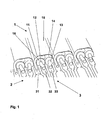
- Fig. 1 shows a known from the prior art and commonly used arrangement.
- a data line 1 is connected to a connection device 2 in addition to several identical data lines.
- the data line 1 has, in addition to a screen 15, a first wire 12 and a second wire 13, which are each surrounded by a cylindrical insulation 16,14.
- the data line 1 has a drain wire 11.
- the printed circuit board 2 has a group of connection pads 3 for the two wires 12, 13 and for the drain wire 11 of the data line 1, namely a first connection pad 31 for the drain wire 11 the first wire 12, a second pad 32 and for the second wire 13, a third pad 33.
- the connection pads 32, 33 of the two wires 12, 13 are next to each other.
- the terminal pad 31 of the drain wire 11 is interposed between the terminal pads of this wire pair 12, 13 and the terminal pads of a pair of wires of an adjacent data line to thereby improve their electrical isolation.
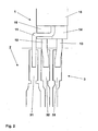
- Fig. 2 shows the same arrangement for the individual data line 1 and for the associated group of connection pads 3 for clarity in a plan view.
- Fig. 3 shows an arrangement according to the invention.
- the edge of the connection device 2 ' is not shown graphically.
- the screen 15 of the data line 1 has a longitudinal section 17. This makes it possible that the two wires 12, 13 are slightly bent away from each other in a set-up area.
- the drain wire 11 is led up between the two insulations 14, 16 and stands in constant mechanical contact with them.
- connection pad 31 'of the drainwire 11 is located between the two connection pads 32', 33 'of the associated pair of wires 12, 13.
- Fig. 4 Here, it is readily apparent that the two wires 11, 12 are bent away from each other over the length of the slot 17 in the erected area. Furthermore, the beginning of the erected area 41 and the end of the erected area 42 are marked. Also in this illustration, the edge of the connection device 2 'is not shown graphically.
- Fig. 5 represents a cross section through the data line 1 in the normal state, that is, for example, at the beginning 41 of the established area.
- the insulation 14, 16 touch each other.
- the two wires have a distance D to each other.
- the first wire 12 has a distance D1 to the drain wire 11.
- Fig. 6 12 illustrates a cross-section through the data line at the end 42 of the erected area.
- the cores are farther apart from one another according to the slot 17 of the screen than in the aforementioned illustration.
- the cores 12, 13 couple into one another essentially via the drainwire 11. This maintains their effective distance.
- the geometric distance D of the two wires 12, 13 increases in the connection region, the effective distance D1 + D2 remains the same, which reduces the irregularities of the impedance in the connection region.
- Fig. 7 illustrates an electrical device according to the invention with a first group of connection pads 3 ', a second group of connection pads 3 "and a third group of connection pads 3"' in a plan view.
- These groups of connection pads 3 ', 3 ", 3"' have different Distances to a rectilinear edge 21 of the printed circuit board 2, ie at least one group 3 "has a different distance from the rectilinear edge 21 than at least one other group of connection pads 3 ', 3"'. If one looks at a straight line 43 which runs through the first group 3 'and the third group 3'', then it can be seen that the second group 3 "does not lie on this line 43.
- connection pads 3 ', 3 ", 3"' are greatly reduced by their staggered arrangement, since in this way the unshielded parts of a data line 1 ', 1 "' in addition shielded parts of another data line 1 "come to rest.
Claims (6)
- Agencement, composé d'un dispositif de raccordement (2) pour des signaux de données à haute fréquence et d'au moins une ligne de données (1) prévue pour le raccordement sur celui-ci, en particulier un câble dit « Twinax », la ligne de données (1) étant adaptée à la transmission de signaux de données à haute fréquence de 10 Gbit/s et plus et présentant trois conducteurs électriques, à savoir un premier brin (12), un deuxième brin (13) et un fil drain (11), les deux brins (12, 13) étant chacun entourés d'une isolation cylindrique (14, 16), et ladite au moins une ligne de données (1) étant entourée d'un blindage (15), par exemple d'une feuille de blindage électriquement conductrice au moins d'un côté, et le dispositif de raccordement (2) présentant pour chaque conducteur électrique un plot de raccordement (31, 32, 33), caractérisé en ce que
le plot de raccordement (31') associé au fil drain (11) respectif est agencé entre les deux plots de raccordement (32', 33') des deux brins (12, 13) appartenant à la même ligne de données (1), le blindage (15) de la ligne de données (1) présentant une section longitudinale (17), et
les deux brins (12, 13) étant légèrement repliés en éloignement l'un de l'autre dans une zone redressée qui présente un début (41) et une fin (42), et en ce que dans cette zone redressée, le fil drain (11) est guidé vers le haut entre les deux isolations (14, 16) et est constamment en contact mécanique avec les isolations associées (14, 16). - Agencement selon la revendication 1, caractérisé en ce que le dispositif de raccordement (2') présente au moins deux groupes de plots de raccordement (3', 3", 3"'), chaque groupe de plots de raccordement (3', 3", 3"') étant prévu pour le raccordement des conducteurs électriques (11, 12, 13) d'une ligne de données respective (1', 1 ", 1'"), le dispositif de raccordement (2') présentant dans son sens de raccordement un bord rectiligne (21), et en ce qu'au moins un groupe de plots de raccordement (3', 3"') présente une autre distance du bord rectiligne (21) qu'au moins un autre groupe (3") de plots de raccordement.
- Agencement selon la revendication 1, caractérisé en ce que le dispositif de raccordement (2') présente au moins trois groupes de plots de raccordement (3', 3", 3"'), chaque groupe de plots de raccordement (3', 3", 3"') étant prévu pour le raccordement des conducteurs électriques (11, 12, 13) d'une ligne de données respective (1', 1", 1 "'), et en ce que l'agencement des groupes de plots de raccordement (3', 3", 3"') sur le dispositif de raccordement (2') diffère d'un agencement rectiligne.
- Procédé d'utilisation d'un agencement selon l'une des revendications 1 à 3, caractérisé en ce que les deux brins (12, 13) sont repliés en éloignement l'un de l'autre dans la zone redressée en ce que le fil drain (11) écarte les isolations associées l'une de l'autre.
- Procédé selon la revendication 4, caractérisé en ce que les deux brins (12, 13) sont légèrement repliés en éloignement l'un de l'autre dans la zone de la fente longitudinale (17).
- Procédé selon la revendication 5, caractérisé en ce que dans la zone de la fente longitudinale (17), le fil drain (11) est pressé entre les isolations (14, 16) des deux brins (12, 13) et assure ainsi une distance effective (D1 + D2) pratiquement constante entre les brins (12, 13).
Applications Claiming Priority (2)
| Application Number | Priority Date | Filing Date | Title |
|---|---|---|---|
| DE102011001225A DE102011001225A1 (de) | 2011-03-11 | 2011-03-11 | Anschlussvorrichtung und Anschlussverfahren für hochfrequente Digitalsignale |
| PCT/DE2012/100044 WO2012122974A1 (fr) | 2011-03-11 | 2012-02-22 | Dispositif et procédé de connexion de signaux numériques à haute fréquence |
Publications (2)
| Publication Number | Publication Date |
|---|---|
| EP2684253A1 EP2684253A1 (fr) | 2014-01-15 |
| EP2684253B1 true EP2684253B1 (fr) | 2015-04-22 |
Family
ID=46061964
Family Applications (1)
| Application Number | Title | Priority Date | Filing Date |
|---|---|---|---|
| EP20120720401 Active EP2684253B1 (fr) | 2011-03-11 | 2012-02-22 | Dispositif et procédé de connexion pour signaux digitaux à haute fréquence |
Country Status (6)
| Country | Link |
|---|---|
| US (1) | US9161436B2 (fr) |
| EP (1) | EP2684253B1 (fr) |
| JP (1) | JP5705339B2 (fr) |
| CN (1) | CN103415959B (fr) |
| DE (1) | DE102011001225A1 (fr) |
| WO (1) | WO2012122974A1 (fr) |
Families Citing this family (11)
| Publication number | Priority date | Publication date | Assignee | Title |
|---|---|---|---|---|
| US9049787B2 (en) * | 2013-01-18 | 2015-06-02 | Molex Incorporated | Paddle card with improved performance |
| WO2015153830A1 (fr) | 2014-04-02 | 2015-10-08 | Molex Incorporated | Système de terminaison de câble |
| CN107636904B (zh) * | 2015-03-18 | 2019-08-20 | 安费诺富加宜(亚洲)私人有限公司 | 电缆组件 |
| EP3121909B1 (fr) * | 2015-07-21 | 2018-09-19 | Delphi Technologies, Inc. | Connecteur électrique à impédance réglée |
| US20190260165A1 (en) * | 2018-02-16 | 2019-08-22 | The Siemon Company | Cable termination for connectors |
| US11374361B2 (en) * | 2018-02-16 | 2022-06-28 | Junkosha Inc. | Plug connector, connector system, and flying body |
| US10643766B1 (en) * | 2018-10-22 | 2020-05-05 | Dell Products L.P. | Drain-aligned cable and method for forming same |
| US11228123B2 (en) | 2018-12-17 | 2022-01-18 | Amphenol Corporation | High performance cable termination |
| US11133569B2 (en) * | 2019-06-14 | 2021-09-28 | Sensorview Incorporated | Compact connector for transmitting super high frequency signal |
| TWM604961U (zh) * | 2020-07-30 | 2020-12-01 | 貿聯國際股份有限公司 | 用於電路板的金屬箔片及具有該金屬箔片的電路裝置 |
| CN112018549A (zh) * | 2020-08-28 | 2020-12-01 | 重庆邮电大学 | 一种适用于麻花针高速传输的外壳 |
Family Cites Families (18)
| Publication number | Priority date | Publication date | Assignee | Title |
|---|---|---|---|---|
| US4508415A (en) | 1983-07-29 | 1985-04-02 | Amp Incorporated | Shielded electrical connector for flat cable |
| US5176538A (en) * | 1991-12-13 | 1993-01-05 | W. L. Gore & Associates, Inc. | Signal interconnector module and assembly thereof |
| CH695034A5 (de) * | 1998-09-30 | 2005-11-15 | Reichle & De Massari Fa | Steckverbindungsteil einer Steckverbindung fuer hochfrequente Datenuebertragung ueber elektrische Leiter. |
| TW456619U (en) * | 1999-07-16 | 2001-09-21 | Molex Inc | Impedance-tuned termination assembly and connectors incorporating same |
| US6217372B1 (en) | 1999-10-08 | 2001-04-17 | Tensolite Company | Cable structure with improved grounding termination in the connector |
| US6857899B2 (en) * | 1999-10-08 | 2005-02-22 | Tensolite Company | Cable structure with improved grounding termination in the connector |
| US6380485B1 (en) | 2000-08-08 | 2002-04-30 | International Business Machines Corporation | Enhanced wire termination for twinax wires |
| JP3645170B2 (ja) | 2000-10-27 | 2005-05-11 | タイコエレクトロニクスアンプ株式会社 | 電気ケーブル端部構造および電気ケーブル端部処理方法 |
| NL1018175C2 (nl) * | 2001-05-30 | 2002-12-03 | Fci Mechelen N V | Stekkerblok en kabelconnector. |
| JP2003346987A (ja) * | 2002-05-27 | 2003-12-05 | Fujikura Ltd | コネクタ付き集合ケーブル |
| JP4083499B2 (ja) * | 2002-08-07 | 2008-04-30 | 株式会社フジクラ | 伝送ケーブルの接続方法及びコネクタ |
| US6739904B2 (en) | 2002-10-04 | 2004-05-25 | Hon Hai Precision Ind. Co., Ltd. | Cable connector assembly |
| JP2004134128A (ja) * | 2002-10-08 | 2004-04-30 | Fujikura Ltd | コネクタ及び伝送ケーブルの接続方法並びにその接続構造 |
| US6955565B2 (en) * | 2002-12-30 | 2005-10-18 | Molex Incorporated | Cable connector with shielded termination area |
| CN1930746B (zh) * | 2004-03-12 | 2010-12-22 | 泛达公司 | 减小电连接器中串扰的方法及装置 |
| JP4216287B2 (ja) * | 2006-02-20 | 2009-01-28 | 日本航空電子工業株式会社 | コネクタ |
| US9124009B2 (en) * | 2008-09-29 | 2015-09-01 | Amphenol Corporation | Ground sleeve having improved impedance control and high frequency performance |
| US8696378B2 (en) * | 2012-02-24 | 2014-04-15 | Tyco Electronics Corporation | Electrical connector assembly and printed circuit board configured to electrically couple to a communication cable |
-
2011
- 2011-03-11 DE DE102011001225A patent/DE102011001225A1/de not_active Ceased
-
2012
- 2012-02-22 EP EP20120720401 patent/EP2684253B1/fr active Active
- 2012-02-22 CN CN201280012776.4A patent/CN103415959B/zh active Active
- 2012-02-22 US US14/002,081 patent/US9161436B2/en active Active
- 2012-02-22 WO PCT/DE2012/100044 patent/WO2012122974A1/fr active Application Filing
- 2012-02-22 JP JP2013558304A patent/JP5705339B2/ja not_active Expired - Fee Related
Also Published As
| Publication number | Publication date |
|---|---|
| JP5705339B2 (ja) | 2015-04-22 |
| EP2684253A1 (fr) | 2014-01-15 |
| JP2014509770A (ja) | 2014-04-21 |
| US9161436B2 (en) | 2015-10-13 |
| WO2012122974A1 (fr) | 2012-09-20 |
| DE102011001225A1 (de) | 2012-09-13 |
| CN103415959A (zh) | 2013-11-27 |
| US20150144391A1 (en) | 2015-05-28 |
| CN103415959B (zh) | 2016-03-16 |
Similar Documents
| Publication | Publication Date | Title |
|---|---|---|
| EP2684253B1 (fr) | Dispositif et procédé de connexion pour signaux digitaux à haute fréquence | |
| EP3170229B1 (fr) | Connecteur et composant et utilisation du connecteur | |
| WO2009138168A1 (fr) | Plaquette de circuit imprimé pour connecteur électrique, et connecteur électrique associé | |
| EP2375501B1 (fr) | Connecteur à fiches pour la réception d'un câble à plusieurs fils | |
| EP2466697B1 (fr) | Module de raccordement de câble de données et procédé destiné à sa confection sur un câble | |
| DE19853666A1 (de) | Elektrischer Verbinder mit Kompensationseinsatz | |
| EP2957003B1 (fr) | Adaptateur | |
| EP2797175B1 (fr) | Fiche pour un câble de données et/ou de télécommunications multi-brins | |
| DE102008027512A1 (de) | Steckverbinder und Verfahren zum Anschluss von elektrischen Leitern an einem Steckverbinder | |
| EP2047571B1 (fr) | Connecteur enfichable pour les techniques de l'informatique et des télécommunications | |
| EP2290753B1 (fr) | Connecteur et platine multicouche | |
| EP2044654B1 (fr) | Bloc de connexion | |
| DE69931591T2 (de) | Leiterplatte für Modularstecker | |
| DE102010034790B4 (de) | Kontaktträger für wenigstens eine Vorrichtung zur Kontaktierung eines elektrischen Leiters mit einer Leiterbahn | |
| EP0954076A2 (fr) | Liaison haute performance de données et de télécommunication avec connecteur à haute densité avec prise et bloc de contact de déplacement | |
| EP2417675B1 (fr) | Boîtier de système à fiches pour câbles multiconducteurs | |
| DE102009010930B4 (de) | Verfahren zum Einspleißen einer Doppelader in mindestens eine bestehende Endteilnehmer-Doppelader und Aderverbinder | |
| EP2207244B1 (fr) | Ensemble de connecteur à fiches et carte de circuit multicouche | |
| EP3080872B1 (fr) | Liaison de contact de lignes de données blindées à une carte de circuits et procédé de mise en contact d'une pluralité de lignes de données blindées avec une carte de circuits | |
| EP3163688B1 (fr) | Élément de connexion destiné à connecter un premier câble de données à un second câble de données et ligne de données comportant un tel élément de connexion. | |
| EP3367514A1 (fr) | Connecteur enfichable pour applications haute fréquence, par exemple, pour application ethernet | |
| DE102018121582A1 (de) | Elektrische Verteilervorrichtung, Montageverfahren und Signalübertragungssystem | |
| EP1168526B1 (fr) | Connecteur pour plaque à circuit intégré | |
| EP2523268B1 (fr) | Prise et système composé d'une prise et d'une douille | |
| DE102016008679A1 (de) | Adapter und Kabel mit Adapter |
Legal Events
| Date | Code | Title | Description |
|---|---|---|---|
| PUAI | Public reference made under article 153(3) epc to a published international application that has entered the european phase |
Free format text: ORIGINAL CODE: 0009012 |
|
| 17P | Request for examination filed |
Effective date: 20130805 |
|
| AK | Designated contracting states |
Kind code of ref document: A1 Designated state(s): AL AT BE BG CH CY CZ DE DK EE ES FI FR GB GR HR HU IE IS IT LI LT LU LV MC MK MT NL NO PL PT RO RS SE SI SK SM TR |
|
| DAX | Request for extension of the european patent (deleted) | ||
| GRAP | Despatch of communication of intention to grant a patent |
Free format text: ORIGINAL CODE: EPIDOSNIGR1 |
|
| INTG | Intention to grant announced |
Effective date: 20141119 |
|
| GRAS | Grant fee paid |
Free format text: ORIGINAL CODE: EPIDOSNIGR3 |
|
| GRAA | (expected) grant |
Free format text: ORIGINAL CODE: 0009210 |
|
| AK | Designated contracting states |
Kind code of ref document: B1 Designated state(s): AL AT BE BG CH CY CZ DE DK EE ES FI FR GB GR HR HU IE IS IT LI LT LU LV MC MK MT NL NO PL PT RO RS SE SI SK SM TR |
|
| REG | Reference to a national code |
Ref country code: GB Ref legal event code: FG4D Free format text: NOT ENGLISH |
|
| REG | Reference to a national code |
Ref country code: CH Ref legal event code: EP |
|
| REG | Reference to a national code |
Ref country code: AT Ref legal event code: REF Ref document number: 723744 Country of ref document: AT Kind code of ref document: T Effective date: 20150515 |
|
| REG | Reference to a national code |
Ref country code: IE Ref legal event code: FG4D Free format text: LANGUAGE OF EP DOCUMENT: GERMAN |
|
| REG | Reference to a national code |
Ref country code: DE Ref legal event code: R096 Ref document number: 502012002932 Country of ref document: DE Effective date: 20150603 |
|
| REG | Reference to a national code |
Ref country code: NL Ref legal event code: VDEP Effective date: 20150422 |
|
| REG | Reference to a national code |
Ref country code: LT Ref legal event code: MG4D |
|
| PG25 | Lapsed in a contracting state [announced via postgrant information from national office to epo] |
Ref country code: NL Free format text: LAPSE BECAUSE OF FAILURE TO SUBMIT A TRANSLATION OF THE DESCRIPTION OR TO PAY THE FEE WITHIN THE PRESCRIBED TIME-LIMIT Effective date: 20150422 |
|
| PG25 | Lapsed in a contracting state [announced via postgrant information from national office to epo] |
Ref country code: HR Free format text: LAPSE BECAUSE OF FAILURE TO SUBMIT A TRANSLATION OF THE DESCRIPTION OR TO PAY THE FEE WITHIN THE PRESCRIBED TIME-LIMIT Effective date: 20150422 Ref country code: ES Free format text: LAPSE BECAUSE OF FAILURE TO SUBMIT A TRANSLATION OF THE DESCRIPTION OR TO PAY THE FEE WITHIN THE PRESCRIBED TIME-LIMIT Effective date: 20150422 Ref country code: LT Free format text: LAPSE BECAUSE OF FAILURE TO SUBMIT A TRANSLATION OF THE DESCRIPTION OR TO PAY THE FEE WITHIN THE PRESCRIBED TIME-LIMIT Effective date: 20150422 Ref country code: NO Free format text: LAPSE BECAUSE OF FAILURE TO SUBMIT A TRANSLATION OF THE DESCRIPTION OR TO PAY THE FEE WITHIN THE PRESCRIBED TIME-LIMIT Effective date: 20150722 Ref country code: PT Free format text: LAPSE BECAUSE OF FAILURE TO SUBMIT A TRANSLATION OF THE DESCRIPTION OR TO PAY THE FEE WITHIN THE PRESCRIBED TIME-LIMIT Effective date: 20150824 Ref country code: FI Free format text: LAPSE BECAUSE OF FAILURE TO SUBMIT A TRANSLATION OF THE DESCRIPTION OR TO PAY THE FEE WITHIN THE PRESCRIBED TIME-LIMIT Effective date: 20150422 |
|
| PG25 | Lapsed in a contracting state [announced via postgrant information from national office to epo] |
Ref country code: IS Free format text: LAPSE BECAUSE OF FAILURE TO SUBMIT A TRANSLATION OF THE DESCRIPTION OR TO PAY THE FEE WITHIN THE PRESCRIBED TIME-LIMIT Effective date: 20150822 Ref country code: RS Free format text: LAPSE BECAUSE OF FAILURE TO SUBMIT A TRANSLATION OF THE DESCRIPTION OR TO PAY THE FEE WITHIN THE PRESCRIBED TIME-LIMIT Effective date: 20150422 Ref country code: GR Free format text: LAPSE BECAUSE OF FAILURE TO SUBMIT A TRANSLATION OF THE DESCRIPTION OR TO PAY THE FEE WITHIN THE PRESCRIBED TIME-LIMIT Effective date: 20150723 Ref country code: LV Free format text: LAPSE BECAUSE OF FAILURE TO SUBMIT A TRANSLATION OF THE DESCRIPTION OR TO PAY THE FEE WITHIN THE PRESCRIBED TIME-LIMIT Effective date: 20150422 |
|
| REG | Reference to a national code |
Ref country code: FR Ref legal event code: PLFP Year of fee payment: 5 |
|
| REG | Reference to a national code |
Ref country code: DE Ref legal event code: R097 Ref document number: 502012002932 Country of ref document: DE |
|
| PG25 | Lapsed in a contracting state [announced via postgrant information from national office to epo] |
Ref country code: EE Free format text: LAPSE BECAUSE OF FAILURE TO SUBMIT A TRANSLATION OF THE DESCRIPTION OR TO PAY THE FEE WITHIN THE PRESCRIBED TIME-LIMIT Effective date: 20150422 Ref country code: DK Free format text: LAPSE BECAUSE OF FAILURE TO SUBMIT A TRANSLATION OF THE DESCRIPTION OR TO PAY THE FEE WITHIN THE PRESCRIBED TIME-LIMIT Effective date: 20150422 |
|
| PLBE | No opposition filed within time limit |
Free format text: ORIGINAL CODE: 0009261 |
|
| STAA | Information on the status of an ep patent application or granted ep patent |
Free format text: STATUS: NO OPPOSITION FILED WITHIN TIME LIMIT |
|
| PG25 | Lapsed in a contracting state [announced via postgrant information from national office to epo] |
Ref country code: CZ Free format text: LAPSE BECAUSE OF FAILURE TO SUBMIT A TRANSLATION OF THE DESCRIPTION OR TO PAY THE FEE WITHIN THE PRESCRIBED TIME-LIMIT Effective date: 20150422 Ref country code: PL Free format text: LAPSE BECAUSE OF FAILURE TO SUBMIT A TRANSLATION OF THE DESCRIPTION OR TO PAY THE FEE WITHIN THE PRESCRIBED TIME-LIMIT Effective date: 20150422 Ref country code: SK Free format text: LAPSE BECAUSE OF FAILURE TO SUBMIT A TRANSLATION OF THE DESCRIPTION OR TO PAY THE FEE WITHIN THE PRESCRIBED TIME-LIMIT Effective date: 20150422 Ref country code: RO Free format text: LAPSE BECAUSE OF NON-PAYMENT OF DUE FEES Effective date: 20150422 |
|
| 26N | No opposition filed |
Effective date: 20160125 |
|
| PG25 | Lapsed in a contracting state [announced via postgrant information from national office to epo] |
Ref country code: IT Free format text: LAPSE BECAUSE OF FAILURE TO SUBMIT A TRANSLATION OF THE DESCRIPTION OR TO PAY THE FEE WITHIN THE PRESCRIBED TIME-LIMIT Effective date: 20150422 |
|
| PG25 | Lapsed in a contracting state [announced via postgrant information from national office to epo] |
Ref country code: SI Free format text: LAPSE BECAUSE OF FAILURE TO SUBMIT A TRANSLATION OF THE DESCRIPTION OR TO PAY THE FEE WITHIN THE PRESCRIBED TIME-LIMIT Effective date: 20150422 Ref country code: BE Free format text: LAPSE BECAUSE OF NON-PAYMENT OF DUE FEES Effective date: 20160229 |
|
| PG25 | Lapsed in a contracting state [announced via postgrant information from national office to epo] |
Ref country code: LU Free format text: LAPSE BECAUSE OF FAILURE TO SUBMIT A TRANSLATION OF THE DESCRIPTION OR TO PAY THE FEE WITHIN THE PRESCRIBED TIME-LIMIT Effective date: 20160222 Ref country code: MC Free format text: LAPSE BECAUSE OF FAILURE TO SUBMIT A TRANSLATION OF THE DESCRIPTION OR TO PAY THE FEE WITHIN THE PRESCRIBED TIME-LIMIT Effective date: 20150422 |
|
| REG | Reference to a national code |
Ref country code: CH Ref legal event code: PL |
|
| GBPC | Gb: european patent ceased through non-payment of renewal fee |
Effective date: 20160222 |
|
| PG25 | Lapsed in a contracting state [announced via postgrant information from national office to epo] |
Ref country code: LI Free format text: LAPSE BECAUSE OF NON-PAYMENT OF DUE FEES Effective date: 20160229 Ref country code: CH Free format text: LAPSE BECAUSE OF NON-PAYMENT OF DUE FEES Effective date: 20160229 |
|
| REG | Reference to a national code |
Ref country code: IE Ref legal event code: MM4A |
|
| REG | Reference to a national code |
Ref country code: FR Ref legal event code: PLFP Year of fee payment: 6 |
|
| PG25 | Lapsed in a contracting state [announced via postgrant information from national office to epo] |
Ref country code: GB Free format text: LAPSE BECAUSE OF NON-PAYMENT OF DUE FEES Effective date: 20160222 Ref country code: IE Free format text: LAPSE BECAUSE OF NON-PAYMENT OF DUE FEES Effective date: 20160222 |
|
| PG25 | Lapsed in a contracting state [announced via postgrant information from national office to epo] |
Ref country code: SE Free format text: LAPSE BECAUSE OF FAILURE TO SUBMIT A TRANSLATION OF THE DESCRIPTION OR TO PAY THE FEE WITHIN THE PRESCRIBED TIME-LIMIT Effective date: 20150422 |
|
| PG25 | Lapsed in a contracting state [announced via postgrant information from national office to epo] |
Ref country code: MT Free format text: LAPSE BECAUSE OF FAILURE TO SUBMIT A TRANSLATION OF THE DESCRIPTION OR TO PAY THE FEE WITHIN THE PRESCRIBED TIME-LIMIT Effective date: 20150422 |
|
| REG | Reference to a national code |
Ref country code: FR Ref legal event code: PLFP Year of fee payment: 7 |
|
| REG | Reference to a national code |
Ref country code: AT Ref legal event code: MM01 Ref document number: 723744 Country of ref document: AT Kind code of ref document: T Effective date: 20170222 |
|
| PG25 | Lapsed in a contracting state [announced via postgrant information from national office to epo] |
Ref country code: HU Free format text: LAPSE BECAUSE OF FAILURE TO SUBMIT A TRANSLATION OF THE DESCRIPTION OR TO PAY THE FEE WITHIN THE PRESCRIBED TIME-LIMIT; INVALID AB INITIO Effective date: 20120222 Ref country code: AT Free format text: LAPSE BECAUSE OF NON-PAYMENT OF DUE FEES Effective date: 20170222 Ref country code: SM Free format text: LAPSE BECAUSE OF FAILURE TO SUBMIT A TRANSLATION OF THE DESCRIPTION OR TO PAY THE FEE WITHIN THE PRESCRIBED TIME-LIMIT Effective date: 20150422 Ref country code: CY Free format text: LAPSE BECAUSE OF FAILURE TO SUBMIT A TRANSLATION OF THE DESCRIPTION OR TO PAY THE FEE WITHIN THE PRESCRIBED TIME-LIMIT Effective date: 20150422 |
|
| PG25 | Lapsed in a contracting state [announced via postgrant information from national office to epo] |
Ref country code: MK Free format text: LAPSE BECAUSE OF FAILURE TO SUBMIT A TRANSLATION OF THE DESCRIPTION OR TO PAY THE FEE WITHIN THE PRESCRIBED TIME-LIMIT Effective date: 20150422 Ref country code: TR Free format text: LAPSE BECAUSE OF FAILURE TO SUBMIT A TRANSLATION OF THE DESCRIPTION OR TO PAY THE FEE WITHIN THE PRESCRIBED TIME-LIMIT Effective date: 20150422 |
|
| PG25 | Lapsed in a contracting state [announced via postgrant information from national office to epo] |
Ref country code: BG Free format text: LAPSE BECAUSE OF FAILURE TO SUBMIT A TRANSLATION OF THE DESCRIPTION OR TO PAY THE FEE WITHIN THE PRESCRIBED TIME-LIMIT Effective date: 20150422 |
|
| PG25 | Lapsed in a contracting state [announced via postgrant information from national office to epo] |
Ref country code: AL Free format text: LAPSE BECAUSE OF FAILURE TO SUBMIT A TRANSLATION OF THE DESCRIPTION OR TO PAY THE FEE WITHIN THE PRESCRIBED TIME-LIMIT Effective date: 20150422 |
|
| PGFP | Annual fee paid to national office [announced via postgrant information from national office to epo] |
Ref country code: FR Payment date: 20230223 Year of fee payment: 12 |
|
| P01 | Opt-out of the competence of the unified patent court (upc) registered |
Effective date: 20230603 |
|
| PGFP | Annual fee paid to national office [announced via postgrant information from national office to epo] |
Ref country code: DE Payment date: 20240228 Year of fee payment: 13 |