EP2677474A1 - Sicheres System zur Verwaltung der Elementleistung - Google Patents
Sicheres System zur Verwaltung der Elementleistung Download PDFInfo
- Publication number
- EP2677474A1 EP2677474A1 EP20120305715 EP12305715A EP2677474A1 EP 2677474 A1 EP2677474 A1 EP 2677474A1 EP 20120305715 EP20120305715 EP 20120305715 EP 12305715 A EP12305715 A EP 12305715A EP 2677474 A1 EP2677474 A1 EP 2677474A1
- Authority
- EP
- European Patent Office
- Prior art keywords
- power
- supply unit
- icc
- pin
- power supply
- Prior art date
- Legal status (The legal status is an assumption and is not a legal conclusion. Google has not performed a legal analysis and makes no representation as to the accuracy of the status listed.)
- Withdrawn
Links
Images


Classifications
-
- G—PHYSICS
- G06—COMPUTING; CALCULATING OR COUNTING
- G06K—GRAPHICAL DATA READING; PRESENTATION OF DATA; RECORD CARRIERS; HANDLING RECORD CARRIERS
- G06K19/00—Record carriers for use with machines and with at least a part designed to carry digital markings
- G06K19/06—Record carriers for use with machines and with at least a part designed to carry digital markings characterised by the kind of the digital marking, e.g. shape, nature, code
- G06K19/067—Record carriers with conductive marks, printed circuits or semiconductor circuit elements, e.g. credit or identity cards also with resonating or responding marks without active components
- G06K19/07—Record carriers with conductive marks, printed circuits or semiconductor circuit elements, e.g. credit or identity cards also with resonating or responding marks without active components with integrated circuit chips
- G06K19/0701—Record carriers with conductive marks, printed circuits or semiconductor circuit elements, e.g. credit or identity cards also with resonating or responding marks without active components with integrated circuit chips at least one of the integrated circuit chips comprising an arrangement for power management
- G06K19/0702—Record carriers with conductive marks, printed circuits or semiconductor circuit elements, e.g. credit or identity cards also with resonating or responding marks without active components with integrated circuit chips at least one of the integrated circuit chips comprising an arrangement for power management the arrangement including a battery
- G06K19/0703—Record carriers with conductive marks, printed circuits or semiconductor circuit elements, e.g. credit or identity cards also with resonating or responding marks without active components with integrated circuit chips at least one of the integrated circuit chips comprising an arrangement for power management the arrangement including a battery the battery being onboard of a handheld device, e.g. a smart phone or PDA
-
- G—PHYSICS
- G06—COMPUTING; CALCULATING OR COUNTING
- G06K—GRAPHICAL DATA READING; PRESENTATION OF DATA; RECORD CARRIERS; HANDLING RECORD CARRIERS
- G06K19/00—Record carriers for use with machines and with at least a part designed to carry digital markings
- G06K19/06—Record carriers for use with machines and with at least a part designed to carry digital markings characterised by the kind of the digital marking, e.g. shape, nature, code
- G06K19/067—Record carriers with conductive marks, printed circuits or semiconductor circuit elements, e.g. credit or identity cards also with resonating or responding marks without active components
- G06K19/07—Record carriers with conductive marks, printed circuits or semiconductor circuit elements, e.g. credit or identity cards also with resonating or responding marks without active components with integrated circuit chips
- G06K19/0701—Record carriers with conductive marks, printed circuits or semiconductor circuit elements, e.g. credit or identity cards also with resonating or responding marks without active components with integrated circuit chips at least one of the integrated circuit chips comprising an arrangement for power management
- G06K19/0702—Record carriers with conductive marks, printed circuits or semiconductor circuit elements, e.g. credit or identity cards also with resonating or responding marks without active components with integrated circuit chips at least one of the integrated circuit chips comprising an arrangement for power management the arrangement including a battery
-
- G—PHYSICS
- G06—COMPUTING; CALCULATING OR COUNTING
- G06K—GRAPHICAL DATA READING; PRESENTATION OF DATA; RECORD CARRIERS; HANDLING RECORD CARRIERS
- G06K19/00—Record carriers for use with machines and with at least a part designed to carry digital markings
- G06K19/06—Record carriers for use with machines and with at least a part designed to carry digital markings characterised by the kind of the digital marking, e.g. shape, nature, code
- G06K19/067—Record carriers with conductive marks, printed circuits or semiconductor circuit elements, e.g. credit or identity cards also with resonating or responding marks without active components
- G06K19/07—Record carriers with conductive marks, printed circuits or semiconductor circuit elements, e.g. credit or identity cards also with resonating or responding marks without active components with integrated circuit chips
- G06K19/0701—Record carriers with conductive marks, printed circuits or semiconductor circuit elements, e.g. credit or identity cards also with resonating or responding marks without active components with integrated circuit chips at least one of the integrated circuit chips comprising an arrangement for power management
- G06K19/0712—Record carriers with conductive marks, printed circuits or semiconductor circuit elements, e.g. credit or identity cards also with resonating or responding marks without active components with integrated circuit chips at least one of the integrated circuit chips comprising an arrangement for power management the arrangement being capable of triggering distinct operating modes or functions dependent on the strength of an energy or interrogation field in the proximity of the record carrier
-
- G—PHYSICS
- G06—COMPUTING; CALCULATING OR COUNTING
- G06K—GRAPHICAL DATA READING; PRESENTATION OF DATA; RECORD CARRIERS; HANDLING RECORD CARRIERS
- G06K19/00—Record carriers for use with machines and with at least a part designed to carry digital markings
- G06K19/06—Record carriers for use with machines and with at least a part designed to carry digital markings characterised by the kind of the digital marking, e.g. shape, nature, code
- G06K19/067—Record carriers with conductive marks, printed circuits or semiconductor circuit elements, e.g. credit or identity cards also with resonating or responding marks without active components
- G06K19/07—Record carriers with conductive marks, printed circuits or semiconductor circuit elements, e.g. credit or identity cards also with resonating or responding marks without active components with integrated circuit chips
- G06K19/0701—Record carriers with conductive marks, printed circuits or semiconductor circuit elements, e.g. credit or identity cards also with resonating or responding marks without active components with integrated circuit chips at least one of the integrated circuit chips comprising an arrangement for power management
- G06K19/0715—Record carriers with conductive marks, printed circuits or semiconductor circuit elements, e.g. credit or identity cards also with resonating or responding marks without active components with integrated circuit chips at least one of the integrated circuit chips comprising an arrangement for power management the arrangement including means to regulate power transfer to the integrated circuit
-
- G—PHYSICS
- G06—COMPUTING; CALCULATING OR COUNTING
- G06K—GRAPHICAL DATA READING; PRESENTATION OF DATA; RECORD CARRIERS; HANDLING RECORD CARRIERS
- G06K19/00—Record carriers for use with machines and with at least a part designed to carry digital markings
- G06K19/06—Record carriers for use with machines and with at least a part designed to carry digital markings characterised by the kind of the digital marking, e.g. shape, nature, code
- G06K19/067—Record carriers with conductive marks, printed circuits or semiconductor circuit elements, e.g. credit or identity cards also with resonating or responding marks without active components
- G06K19/07—Record carriers with conductive marks, printed circuits or semiconductor circuit elements, e.g. credit or identity cards also with resonating or responding marks without active components with integrated circuit chips
- G06K19/0723—Record carriers with conductive marks, printed circuits or semiconductor circuit elements, e.g. credit or identity cards also with resonating or responding marks without active components with integrated circuit chips the record carrier comprising an arrangement for non-contact communication, e.g. wireless communication circuits on transponder cards, non-contact smart cards or RFIDs
- G06K19/0727—Record carriers with conductive marks, printed circuits or semiconductor circuit elements, e.g. credit or identity cards also with resonating or responding marks without active components with integrated circuit chips the record carrier comprising an arrangement for non-contact communication, e.g. wireless communication circuits on transponder cards, non-contact smart cards or RFIDs the arrangement being a circuit facilitating integration of the record carrier with a hand-held device such as a smart phone of PDA
-
- H—ELECTRICITY
- H02—GENERATION; CONVERSION OR DISTRIBUTION OF ELECTRIC POWER
- H02J—CIRCUIT ARRANGEMENTS OR SYSTEMS FOR SUPPLYING OR DISTRIBUTING ELECTRIC POWER; SYSTEMS FOR STORING ELECTRIC ENERGY
- H02J9/00—Circuit arrangements for emergency or stand-by power supply, e.g. for emergency lighting
- H02J9/04—Circuit arrangements for emergency or stand-by power supply, e.g. for emergency lighting in which the distribution system is disconnected from the normal source and connected to a standby source
- H02J9/06—Circuit arrangements for emergency or stand-by power supply, e.g. for emergency lighting in which the distribution system is disconnected from the normal source and connected to a standby source with automatic change-over, e.g. UPS systems
- H02J9/061—Circuit arrangements for emergency or stand-by power supply, e.g. for emergency lighting in which the distribution system is disconnected from the normal source and connected to a standby source with automatic change-over, e.g. UPS systems for DC powered loads
Definitions
- the present disclosure relates to wireless communications and, more particularly, to the power management of a secure element of a wireless device. It finds applications, for instance, in wireless devices such as smart phones or digital tablets.
- wireless devices functionalities have increased enormously and not only for making phone calls, but also for performing applications like capturing images, watching videos, surfing over the Internet, sending and receiving emails, listening to music or enjoying other entertainments, using geo-localisation based tools, etc.. Such features stretch the boundaries of power available in a wireless device.
- NFC Near Field Communication
- NFC is a short range communication technology that allows a portable, e.g. wireless device to emulate both a contactless tag and a contactless reader. It provides an easy way for users to interact with their environment.
- NFC is currently seen as an enabling technology for a number of applications such as mobile payment and public transportation ticketing, for instance.
- a Universal Integrated Circuit Card containing applications such as a SIM (Subscriber Identity Module) card, USIM (Universal Subscriber Identity Module) card or ISIM (IP Multimedia Services Identity Module), is utilised as a Secure Element (SE) to hold sensitive information securely.
- SIM Subscriber Identity Module
- USIM Universal Subscriber Identity Module
- ISIM IP Multimedia Services Identity Module
- SE Secure Element
- NFC platforms readily available on the market feature an existing UICC power supply system, which however is not designed to serve the specific needs of the SE.
- NFC secure applications are designed so as be able to run even when the wireless device is in a battery-Off mode of operation wherein, for instance, the battery of the mobile phone is discharged or dismounted.
- the above problems may be overcome by enabling the supply of power to a universal integrated circuit card (UICC) being in a battery-Off mode, by using power from a circuit with a single connection from the circuit to the legacy power path of the UICC.
- UICC universal integrated circuit card
- a first aspect of the proposed solution relates to a circuit for supplying power to an integrated circuit card (ICC) of a wireless device comprising a first power supply unit adapted to supply power to the ICC through a first power path in a first operation mode of the device while being unable to supply power to the ICC in a second operation mode of the device.
- the circuit comprises:
- a second aspect relates to a method of supplying power to an integrated circuit card (ICC) of a wireless device comprising a first power supply unit.
- the method comprises:
- a third aspect relates to a first power supply unit comprising:
- a fourth aspect relates to a wireless device comprising:
- the circuit further comprises a control output pin connected to the controller and adapted to be connected to a circuit breaking unit of the device located in the first power path between the first power supply unit and a connection point between the first power path on one side, and the second and third power path on the other side.
- the controller is configured to control the opening of the circuit breaking unit through the control pin so as to prevent back current flow from the second power unit to the first power supply unit in the second operation mode of the device.
- the controller is configured to determine whether the device operates in the second operation mode and/or the first power supply unit is unable to supply power to the ICC; and, based on said determination, to control operation of the power pin as a power input pin or as a power output pin, and/or to control the opening or closing of the circuit breaking device.
- the device operating in the second operation mode is determined based on information obtained by the controller from a central processor of the device.
- the first power supply unit being unable to supply power to the ICC is determined by monitoring a current flow entering the power pin when the power pin is configured to operate in the first operation mode of the device.
- the first power supply unit is considered to be unable to supply power to the ICC if the current flow entering the power pin during a given period of time when the power pin is configured to operate in the first operation mode of the device, is below a given threshold.
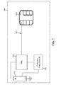
- FIG. 1 is a block diagram illustrating prior art power system adapted to supply power to an ICC 140.
- a wireless device 100 comprising a battery 110, a first power supply unit 120, a central processor 130 and a first power path 101.
- the central processor 130 controls overall operation of the wireless device 100, the latter having at least some of the following functionalities: management of incoming and outgoing phone call, management of voice communication including speech data acquisition/restitution, encoding/decoding, modulating/demodulating, transmitting/receiving, and so on.
- the processor 130 may be integrated in e.g. the digital baseband processor or may be a discrete, e.g. dedicated processor, microcontroller, or the like.
- the first power supply unit 120 which may be a power management unit or at least a part thereof, is responsible for managing the supply of power from the battery 110 to the ICC 140 through the first power path 101.
- the battery 110 may be, for instance, the main source of energy of the wireless device 100 circuitry and subsystems, or an additional, e.g. dedicated power storing device.
- the wireless device 100 is set into a particular one of a plurality of operation modes.
- At least three modes can be provided as follows: a "Full Power mode", a “Low Power mode” and a “Battery OFF mode”.
- “Full Power mode” applies when the wireless device 100 is switched on and all the functionalities are made available to the user.
- Low Power mode applies when the wireless device 100 is in an energy saving mode or is switched off with the battery 110 still containing a low residual power. In this mode, all the functionalities of the wireless device 100 are shut down, except the clock module and some few other functions. The wireless device may be put in this mode, either by the user or automatically, for instance when the available power is below a first threshold of the battery 110.
- Battery OFF mode applies when the battery 110 of the wireless device 100 is discharged or dismounted whereby no functionalities are available at all.
- the proposed solution addresses situations when the device is in the latter mode.
- the UICC may be utilised as a Secure Element (SE) to hold sensitive information used by the device.
- SE Secure Element
- existing UICC power supply systems readily available to application designers are not adapted to serve the specific needs of the NFC SE (NFC Secure Element).
- the NFC SE is designed to run even when the wireless device 100 is in a battery-Off mode.
- FIG. 2 is a block diagram illustrating an exemplary implementation of the proposed solution to that problem.
- the wireless device 100 of FIG. 1 further including a circuit 150.
- the circuit might be an NFC integrated circuit and is connected to the central processor 130.
- the circuit comprises a controller 152, a second power supply unit 151, a power pin 153 and a data communication pin 154.
- the communication pin 154 is connected to the ICC 140 in order to enable data and control exchange, for instance by using a protocol such as SWP (Single Wire Protocol).
- SWP Single Wire Protocol
- the controller 152 is configured to operate the power pin 153, the latter being also connected to the second power supply unit 151 and to a connection point 160 between the first power path 101 and a second power path 102.
- the second power supply unit 151 is responsible for managing the power supply from a near field communication antenna 170 to the power pin 153.
- the ICC 140 is supplied with power from the first power supply unit 120.
- the power pin 153 is configured to operate as a power input pin. In such configuration of pin 153, power coming from the first power supply unit 120 may enter the circuit 150, via the connection point 160 and through the power path 102 and the power pin 153 without damaging the circuit 150.
- the ICC 140 is supplied with power from the first power supply unit 120.
- a power pin 121 attached to the first power supply unit 120 may not have any impact on the power coming from the first power supply unit 120.
- the power pin 153 is configured to operate as a power output pin.
- power coming from the near field communication antenna 170 may be carried to the connection point 160 by the second power supply unit 151 through the power pin 153 and the power path 102.
- the power coming from the near field communication antenna 170 may then flows through the power path 103.
- the ICC 140 is supplied in power by the second power supply unit 151.
- the power coming from the near field communication antenna 170 may also be flows through the power path 101.
- the first power supply unit 120 is adapted to withstand the ingress of this unwanted power thanks to the power pin 121 thus preventing any damage of the first power supply unit 120.
- the power pin 121 may comprise at least a diode to prevent the back current flow into the first power supply unit 120, for instance, while the wireless device 100 is in the second operation mode, that is to say in the "Battery OFF mode" of the above mentioned example.
- FIG. 3 is a graph illustrating an example of implementation of the proposed solution.
- the wireless device 100 of FIG. 2 further including a control pin 155 on the circuit 150 and a circuit breaking device 180 arranged in the first power path 101.
- the control pin 155 is connected to the controller 152 and to the circuit breaking device 180.
- the circuit breaking device may be located between the first power supply unit 120 and the connection point 160.
- the controller 152 is configured to operate the circuit breaking device 180 through the control pin 155.
- the power pin 153 is configured to operate as a power input pin. In such configuration of pin 153, power coming from the first power supply unit 120 may enter the circuit 150, via the connection point 160 and through the power path 102 and the power pin 153 without damaging the circuit 150.
- the controller 152 may also operate at the same time the circuit breaking device 180 to let the power normally flow over the first power path 101 while the wireless device 100 is in the "Full Power mode” or in the "Low Power mode".
- the ICC 140 is supplied in power by the first power supply unit 120.
- the power pin 153 is configured to operate as a power output pin.
- power coming from the near field communication antenna 170, by induction for instance, may be carried to the connection point 160 by the second power supply unit 151 through the power pin 153.
- the ICC 140 is supplied in power by the second power supply unit 151.
- the controller 152 may also operate at the same time the circuit breaking device 180 to cut off the first power path 101 in order to prevent back current flow from the second power supply unit 151 in the first power supply unit 120 via the connection point 160 while the wireless device 100 is in a "Battery OFF mode".
- the circuit breaking device 180 aims at shielding the first power supply unit 120 against potential severe damages.
- the controller 152 is capable of determining whether the first power supply unit 120 is unable to supply power to the ICC, that is to say in the "Battery OFF mode".
- the controller 152 may operate the power pin 153 to selectively act as power input pin or as power output pin.
- the controller 152 may, at the same time, operate the circuit breaking device 180 to let the current flow normally on the first power path 101 or to cut off the first power path 101.
- the knowledge of the first power supply unit 120 being in the second operation may be obtained from the central processor 130 to which the circuit 150 is connected to.
- the central processor 130 may, for instance, give indication to the controller 152 about the wireless device 100 state or about the amount of residual power available in the battery 110 of the wireless device 110. At least the latter information and some others may be manipulated by the controller 152 to determine the subsequent operations to trigger.
- the controller 152 may determine whether the first power supply unit 120 is unable to supply power to the ICC, that is to say in the "Battery OFF mode" by monitoring the current flow entering the power pin 153 while being configured to operate as a power input pin. Hence, for instance, if during a given period of time there is no current flow entering the power pin 153, the controller 152 can deduce that the first power supply unit 120 is in a "Battery OFF mode".
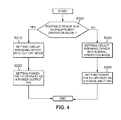
- FIG. 4 is a flow diagram illustrating embodiments of the proposed method consistent with the embodiment of the wireless device 100 already described above with FIG. 3 . Depending on the embodiment, additional steps may be added, others removed, and the ordering of the steps rearranged.
- step S200 a test is performed to establish whether the wireless device 100 is in a second operation mode.
- the second operation mode being, for instance, the "Battery OFF mode" as already described beforehand.
- the circuit breaking device 180 is set into a cut off mode as already described in FIG. 3 .
- step S220 the power pin 153 is set to operate as a power output pin as already described in FIG. 3 . After that, the algorithm would stop.
- the circuit breaking device 180 is set into normal operation mode as already described in FIG. 3 such that the current would normally flow through the first power path 101.
- a step S240 the power pin 153 is set to operate as a power input pin as already described in FIG. 3 . After that, the algorithm would stop.
Priority Applications (3)
| Application Number | Priority Date | Filing Date | Title |
|---|---|---|---|
| EP20120305715 EP2677474A1 (de) | 2012-06-21 | 2012-06-21 | Sicheres System zur Verwaltung der Elementleistung |
| PCT/EP2013/062800 WO2013190010A1 (en) | 2012-06-21 | 2013-06-19 | Secure element power management system |
| US14/405,216 US9202158B2 (en) | 2012-06-21 | 2013-06-19 | Secure element power management system |
Applications Claiming Priority (1)
| Application Number | Priority Date | Filing Date | Title |
|---|---|---|---|
| EP20120305715 EP2677474A1 (de) | 2012-06-21 | 2012-06-21 | Sicheres System zur Verwaltung der Elementleistung |
Publications (1)
| Publication Number | Publication Date |
|---|---|
| EP2677474A1 true EP2677474A1 (de) | 2013-12-25 |
Family
ID=46650462
Family Applications (1)
| Application Number | Title | Priority Date | Filing Date |
|---|---|---|---|
| EP20120305715 Withdrawn EP2677474A1 (de) | 2012-06-21 | 2012-06-21 | Sicheres System zur Verwaltung der Elementleistung |
Country Status (3)
| Country | Link |
|---|---|
| US (1) | US9202158B2 (de) |
| EP (1) | EP2677474A1 (de) |
| WO (1) | WO2013190010A1 (de) |
Cited By (1)
| Publication number | Priority date | Publication date | Assignee | Title |
|---|---|---|---|---|
| FR3099609A1 (fr) * | 2019-07-29 | 2021-02-05 | Commissariat à l'Energie Atomique et aux Energies Alternatives | Carte électronique intelligente, de type carte à puce intégrant un système d'alimentation électrique à cellules électriques en Li/MnO2 |
Families Citing this family (2)
| Publication number | Priority date | Publication date | Assignee | Title |
|---|---|---|---|---|
| CN107147432A (zh) * | 2017-06-14 | 2017-09-08 | Tcl移动通信科技(宁波)有限公司 | 一种检测nfc启动的移动终端及其实现方法、存储装置 |
| US10921870B2 (en) * | 2018-09-25 | 2021-02-16 | Quanta Computer Inc. | System and method for hybrid power supply |
Citations (2)
| Publication number | Priority date | Publication date | Assignee | Title |
|---|---|---|---|---|
| EP1280099A1 (de) * | 2001-03-02 | 2003-01-29 | Sony Corporation | Chip für kontaktlose lese-/schreibvorrichtung mit funktion zur verwaltung der stromversorgung |
| FR2888974A1 (fr) * | 2005-07-25 | 2007-01-26 | Gemplus Sa | Procede et systeme de communication radiofrequence avec un module electronique a contacts electriques, module et dispositif associes |
Family Cites Families (8)
| Publication number | Priority date | Publication date | Assignee | Title |
|---|---|---|---|---|
| JPH0449485A (ja) * | 1990-06-19 | 1992-02-18 | Mitsubishi Electric Corp | Icカード |
| JP3487428B2 (ja) * | 2000-10-31 | 2004-01-19 | 松下電器産業株式会社 | 電源回路および非接触icカード |
| JP3964182B2 (ja) * | 2001-11-02 | 2007-08-22 | 株式会社ルネサステクノロジ | 半導体装置 |
| KR101053185B1 (ko) * | 2005-02-24 | 2011-08-01 | 삼성전자주식회사 | 스마트 카드 및 그것의 혼합모드 제어방법 |
| JP2009054061A (ja) * | 2007-08-29 | 2009-03-12 | Renesas Technology Corp | 半導体装置 |
| JP5258490B2 (ja) * | 2008-10-02 | 2013-08-07 | ルネサスエレクトロニクス株式会社 | 半導体集積回路及びそれを用いたicカード |
| US8833666B2 (en) * | 2012-03-09 | 2014-09-16 | Infineon Technologies Ag | Smart card device |
| TWI459188B (zh) * | 2012-03-09 | 2014-11-01 | Phison Electronics Corp | 具智慧卡功能的記憶卡及其電源控制方法與電源控制電路 |
-
2012
- 2012-06-21 EP EP20120305715 patent/EP2677474A1/de not_active Withdrawn
-
2013
- 2013-06-19 US US14/405,216 patent/US9202158B2/en active Active
- 2013-06-19 WO PCT/EP2013/062800 patent/WO2013190010A1/en active Application Filing
Patent Citations (2)
| Publication number | Priority date | Publication date | Assignee | Title |
|---|---|---|---|---|
| EP1280099A1 (de) * | 2001-03-02 | 2003-01-29 | Sony Corporation | Chip für kontaktlose lese-/schreibvorrichtung mit funktion zur verwaltung der stromversorgung |
| FR2888974A1 (fr) * | 2005-07-25 | 2007-01-26 | Gemplus Sa | Procede et systeme de communication radiofrequence avec un module electronique a contacts electriques, module et dispositif associes |
Cited By (1)
| Publication number | Priority date | Publication date | Assignee | Title |
|---|---|---|---|---|
| FR3099609A1 (fr) * | 2019-07-29 | 2021-02-05 | Commissariat à l'Energie Atomique et aux Energies Alternatives | Carte électronique intelligente, de type carte à puce intégrant un système d'alimentation électrique à cellules électriques en Li/MnO2 |
Also Published As
| Publication number | Publication date |
|---|---|
| WO2013190010A1 (en) | 2013-12-27 |
| US20150108225A1 (en) | 2015-04-23 |
| US9202158B2 (en) | 2015-12-01 |
Similar Documents
| Publication | Publication Date | Title |
|---|---|---|
| US8725110B2 (en) | Mobile communication terminal and method for managing SIM cards | |
| US7912441B2 (en) | Apparatus and method for enabling near field communication equipment in a portable communications device | |
| US9729205B2 (en) | Battery management scheme for NFC | |
| US9583975B2 (en) | Charging and audio usage | |
| US8280347B2 (en) | Method and apparatus for automatically damaging circuitry of a mobile device when one or more conditions are detected | |
| EP3116161A1 (de) | Verfahren zur verwaltung einer sicherheitseinheit und endgerät | |
| US20070103434A1 (en) | Portable communication device and power saving method used therein | |
| US20120108169A1 (en) | Method and device for managing information exchange between for example a nfc controller and a set of at least two secure elements | |
| CN108091808B (zh) | 电池、设备、充电控制方法及装置 | |
| CN101022657B (zh) | 移动通信设备及对通信路径的选择性使用进行控制的方法 | |
| CN110225576A (zh) | 一种开机控制方法与电子设备 | |
| CN103152472A (zh) | 通信装置及其控制方法、摄像装置及其控制方法 | |
| CN107703348A (zh) | 智能插座的检测方法及装置 | |
| US9202158B2 (en) | Secure element power management system | |
| CN109565381B (zh) | 信息反馈方法及装置 | |
| CN111523633B (zh) | 数据传输方法、多功能卡及电子设备 | |
| US11388574B2 (en) | Methods and apparatus for providing access to emergency service providers | |
| CN113451669A (zh) | 充电方法及装置、电子设备、存储介质 | |
| CN106658674B (zh) | 移动终端及输出传导功率的方法 | |
| KR100746548B1 (ko) | 내장 배터리를 이용하여 현재 위치 정보를 전송하는이동통신 단말기 및 방법 | |
| KR101318654B1 (ko) | 가입자 인증 모듈 카드에 따른 이동통신 단말기 제어 방법 | |
| EP2706431A1 (de) | Mobiles endgerät und aufzeichnungsmedium | |
| CN103929545A (zh) | 一种移动终端及其网络异常提示方法 | |
| US20150334558A1 (en) | Methods for configuring a mobile device and related mobile devices | |
| US7693554B2 (en) | Method for operating a data storage medium |
Legal Events
| Date | Code | Title | Description |
|---|---|---|---|
| PUAI | Public reference made under article 153(3) epc to a published international application that has entered the european phase |
Free format text: ORIGINAL CODE: 0009012 |
|
| AK | Designated contracting states |
Kind code of ref document: A1 Designated state(s): AL AT BE BG CH CY CZ DE DK EE ES FI FR GB GR HR HU IE IS IT LI LT LU LV MC MK MT NL NO PL PT RO RS SE SI SK SM TR |
|
| AX | Request for extension of the european patent |
Extension state: BA ME |
|
| 17P | Request for examination filed |
Effective date: 20140624 |
|
| RBV | Designated contracting states (corrected) |
Designated state(s): AL AT BE BG CH CY CZ DE DK EE ES FI FR GB GR HR HU IE IS IT LI LT LU LV MC MK MT NL NO PL PT RO RS SE SI SK SM TR |
|
| RAP1 | Party data changed (applicant data changed or rights of an application transferred) |
Owner name: OCT CIRCUIT TECHNOLOGIES INTERNATIONAL LIMITED |
|
| STAA | Information on the status of an ep patent application or granted ep patent |
Free format text: STATUS: THE APPLICATION HAS BEEN WITHDRAWN |
|
| 18W | Application withdrawn |
Effective date: 20180706 |