EP2671256B1 - Schutzeinrichtung für eine photovoltaikanlage - Google Patents
Schutzeinrichtung für eine photovoltaikanlage Download PDFInfo
- Publication number
- EP2671256B1 EP2671256B1 EP11720111.1A EP11720111A EP2671256B1 EP 2671256 B1 EP2671256 B1 EP 2671256B1 EP 11720111 A EP11720111 A EP 11720111A EP 2671256 B1 EP2671256 B1 EP 2671256B1
- Authority
- EP
- European Patent Office
- Prior art keywords
- output
- voltage
- protective device
- current
- signal
- Prior art date
- Legal status (The legal status is an assumption and is not a legal conclusion. Google has not performed a legal analysis and makes no representation as to the accuracy of the status listed.)
- Active
Links
Images

Classifications
-
- H—ELECTRICITY
- H02—GENERATION; CONVERSION OR DISTRIBUTION OF ELECTRIC POWER
- H02H—EMERGENCY PROTECTIVE CIRCUIT ARRANGEMENTS
- H02H3/00—Emergency protective circuit arrangements for automatic disconnection directly responsive to an undesired change from normal electric working condition with or without subsequent reconnection ; integrated protection
- H02H3/02—Details
-
- H—ELECTRICITY
- H02—GENERATION; CONVERSION OR DISTRIBUTION OF ELECTRIC POWER
- H02S—GENERATION OF ELECTRIC POWER BY CONVERSION OF INFRARED RADIATION, VISIBLE LIGHT OR ULTRAVIOLET LIGHT, e.g. USING PHOTOVOLTAIC [PV] MODULES
- H02S50/00—Monitoring or testing of PV systems, e.g. load balancing or fault identification
-
- G—PHYSICS
- G01—MEASURING; TESTING
- G01R—MEASURING ELECTRIC VARIABLES; MEASURING MAGNETIC VARIABLES
- G01R19/00—Arrangements for measuring currents or voltages or for indicating presence or sign thereof
- G01R19/165—Indicating that current or voltage is either above or below a predetermined value or within or outside a predetermined range of values
-
- G—PHYSICS
- G01—MEASURING; TESTING
- G01R—MEASURING ELECTRIC VARIABLES; MEASURING MAGNETIC VARIABLES
- G01R31/00—Arrangements for testing electric properties; Arrangements for locating electric faults; Arrangements for electrical testing characterised by what is being tested not provided for elsewhere
- G01R31/12—Testing dielectric strength or breakdown voltage ; Testing or monitoring effectiveness or level of insulation, e.g. of a cable or of an apparatus, for example using partial discharge measurements; Electrostatic testing
-
- H—ELECTRICITY
- H02—GENERATION; CONVERSION OR DISTRIBUTION OF ELECTRIC POWER
- H02J—CIRCUIT ARRANGEMENTS OR SYSTEMS FOR SUPPLYING OR DISTRIBUTING ELECTRIC POWER; SYSTEMS FOR STORING ELECTRIC ENERGY
- H02J3/00—Circuit arrangements for AC mains or AC distribution networks
- H02J3/38—Arrangements for parallely feeding a single network by two or more generators, converters or transformers
-
- H—ELECTRICITY
- H02—GENERATION; CONVERSION OR DISTRIBUTION OF ELECTRIC POWER
- H02M—APPARATUS FOR CONVERSION BETWEEN AC AND AC, BETWEEN AC AND DC, OR BETWEEN DC AND DC, AND FOR USE WITH MAINS OR SIMILAR POWER SUPPLY SYSTEMS; CONVERSION OF DC OR AC INPUT POWER INTO SURGE OUTPUT POWER; CONTROL OR REGULATION THEREOF
- H02M7/00—Conversion of AC power input into DC power output; Conversion of DC power input into AC power output
-
- H—ELECTRICITY
- H02—GENERATION; CONVERSION OR DISTRIBUTION OF ELECTRIC POWER
- H02S—GENERATION OF ELECTRIC POWER BY CONVERSION OF INFRARED RADIATION, VISIBLE LIGHT OR ULTRAVIOLET LIGHT, e.g. USING PHOTOVOLTAIC [PV] MODULES
- H02S40/00—Components or accessories in combination with PV modules, not provided for in groups H02S10/00 - H02S30/00
- H02S40/30—Electrical components
- H02S40/32—Electrical components comprising DC/AC inverter means associated with the PV module itself, e.g. AC modules
-
- H—ELECTRICITY
- H10—SEMICONDUCTOR DEVICES; ELECTRIC SOLID-STATE DEVICES NOT OTHERWISE PROVIDED FOR
- H10F—INORGANIC SEMICONDUCTOR DEVICES SENSITIVE TO INFRARED RADIATION, LIGHT, ELECTROMAGNETIC RADIATION OF SHORTER WAVELENGTH OR CORPUSCULAR RADIATION
- H10F77/00—Constructional details of devices covered by this subclass
- H10F77/95—Circuit arrangements
- H10F77/953—Circuit arrangements for devices having potential barriers
- H10F77/955—Circuit arrangements for devices having potential barriers for photovoltaic devices
-
- Y—GENERAL TAGGING OF NEW TECHNOLOGICAL DEVELOPMENTS; GENERAL TAGGING OF CROSS-SECTIONAL TECHNOLOGIES SPANNING OVER SEVERAL SECTIONS OF THE IPC; TECHNICAL SUBJECTS COVERED BY FORMER USPC CROSS-REFERENCE ART COLLECTIONS [XRACs] AND DIGESTS
- Y02—TECHNOLOGIES OR APPLICATIONS FOR MITIGATION OR ADAPTATION AGAINST CLIMATE CHANGE
- Y02E—REDUCTION OF GREENHOUSE GAS [GHG] EMISSIONS, RELATED TO ENERGY GENERATION, TRANSMISSION OR DISTRIBUTION
- Y02E10/00—Energy generation through renewable energy sources
- Y02E10/50—Photovoltaic [PV] energy
Definitions
- the invention relates to a protective device for a photovoltaic system, which has at least one input for connection to a photovoltaic generator and at least one output for delivering an electric power supplied by the photovoltaic generator.
- the invention further relates to a photovoltaic module with a protective device and an operating method for a protective device of a photovoltaic system.
- Photovoltaic systems are used to convert sunlight into electrical energy.
- a plurality of photovoltaic modules abbreviated to photovoltaic modules in the following, each of which represents an interconnection of a plurality of photovoltaic cells, are electrically interconnected as a photovoltaic generator.
- the photovoltaic (PV) generator is connected to a frequently remotely mounted inverter which serves to convert the DC power supplied by the PV generator into AC suitable for feeding into a public or private (stand alone) utility grid.
- the PV modules are usually connected in series in such a way that the DC lines extending between the PV generator and the inverter are subjected to voltages in the range of significantly more than 100 V.
- a voltage of this magnitude is useful for reasons of efficiency, inter alia to keep resistive losses in the lines bearable small, without having to choose an excessively large cable cross-section.
- the danger to life in direct contact or indirect contact eg. B. on extinguishing water, only ban if the power generation is prevented by the PV modules, for example by a darkening of the PV modules.
- switching elements eg. Contactors or semiconductor switches arranged to switch the connection lines between the PV modules and the inverter disconnected from the inverter or other control unit via central lines. This can be done by interrupting the connection lines through the switching elements or by shorting the PV modules, such as in the Photon magazine, May 2005 issue, pp. 75-77 disclosed.
- the connecting lines between the PV generator and the inverter can also, as in the publication DE 10 2005 018 173 A1 as well as in the publication WO 2010/078303 A2 disclosed to be de-energized by a single, arranged on the PV generator switching device.
- control lines For the transmission of the control signals to the switching elements additionally laid control lines are used, but this is associated with an increased installation costs, especially in large PV systems.
- As an alternative is from the document DE 10 2006 060 815 A1 known to apply the control signals as high-frequency signals by means of a transformer to the DC power transmission lines and to transmit over this.
- the switching elements are provided for this purpose with a control unit which the decoded high-frequency transmitted control signals and controls the switching process. This solution is complicated, since a material-intensive transformer is needed to apply the control signals in view of the high currents on the DC lines.
- the protective device has a detection device for a signal supplied via the at least one output and is set up to provide a low-voltage limited voltage at the output, if a supplied signal does not satisfy predetermined criteria is sufficient, and that the output is connected via a switching device of low resistance to the at least one input, if the signal supplied meets the predetermined criteria.
- the protective device which is preferably arranged spatially as close as possible to the PV generator and is connected with its input to the PV generator and with its output to a possibly remotely positioned inverter, the output initially only with the harmless low voltage. In this way, the information is transmitted by the protective device that there is an irradiation on the PV generator. Only when an inverter (or other generator remote device) responsive thereto and settles a predetermined signal, the protection device connects the output via the switching device low-impedance to its input and thus acts on the DC connection line to the inverter with the full voltage of the PV generator, or in other words, switches the PV generator on the DC lines, which then the entire power of the PV generator can be transmitted to the inverter.
- the predetermined criterion is no longer met, for example because the predetermined signal is eliminated.
- the input and output of the protective device are separated from each other by the switching element and the output is again acted upon only with the harmless low voltage.
- the detection device has a current measuring device for a current delivered to the at least one output current, wherein the supplied signal is associated with a level of the current.
- the detection device has a voltage measuring device for a voltage applied to the at least one output voltage, wherein the supplied signal is associated with a level of the voltage.
- the predetermined criteria relate to a temporal modulation of the signal, in particular a pulse pattern. In this way, a reliable detection of a switch-on signal is achieved.
- the predetermined criteria relate to the magnitude of the current delivered to the at least one output
- the protection device is adapted to provide the extra-low voltage at the at least one output if the output current is less than a lower threshold and the at least one Output via the switching device low resistance to the at least one input to connect when the output current is greater than or equal to an upper threshold where the upper threshold is greater than or equal to the lower threshold.
- the protective device connects the PV generator to the DC lines when an inverter loads its DC voltage applied to this low voltage, and a current above or at the upper threshold current is detected at the output of the protective device.
- the inverter is switched off, e.g. In the event of danger, conversely, the DC input of the inverter and thus the output of the protective device is no longer loaded and the input and output of the protective device are separated again by the switching element.
- the threshold values for the current flow should be chosen such that a connection of the output of the protective device to the input by touching the DC connecting lines, by a greatly reduced insulation resistance or by the conductivity of (extinguishing) water is excluded.
- this has a further input to supply a partial voltage of the PV generator for immediate provision or for generating the extra-low voltage.
- the low voltage can be provided particularly economically without or with minimal change losses.
- the low voltage is connected via a series resistor high impedance to the at least one output. This ensures, inter alia, that with several protective devices connected in parallel at their outputs, a current flow at each of the protective devices sets when the low voltage is loaded, and thus each of the protective devices can perform its switching function.
- this has a device for arc detection, which is connected to the switching element to its control.
- the device for arc detection is preferred connected to the switching member such that the switching member separates when an arc is detected.
- the protective device can also be used for automatically extinguishing arcing.
- the integration of voltage protection and arc quenching in the protective device allows economical use of components, such as those elements such as the switching element, which is used in both cases.
- the object is achieved by a PV module having such an integrated protection device.
- a PV module having such an integrated protection device.
- Such a PV module can be used in the same way as known PV modules within PV systems and offers the advantages described above in connection with the protective device without further measures.
- the protective device is arranged in a junction box of the PV module, which allows a particularly compact design.
- the object is achieved by an operating method for a protective device of a PV system, the protective device having at least one input for connection to a PV generator and at least one output for outputting electrical power provided by the PV generator ,
- the operating method has the following steps: The at least one output is subjected to a low voltage and is monitored for the presence of a signal, wherein a present signal is optionally detected.
- the at least one output is supplied with an operating voltage for outputting the entire electric power provided by the PV generator when a detected signal satisfies predetermined criteria. If no signal is present or if the detected signal does not satisfy predetermined criteria, the output is again supplied with the low voltage.
- FIG. 1 schematically shows the basic structure of a PV system with a protective device in a first embodiment.
- the PV system has a PV generator 1, which is connected via connecting lines 2 to inputs 101 and 102 of a protective device 100.
- the protective device 100 also has outputs 103 and 104, from which DC lines 3 lead to an inverter 4, which is connected to a power supply network 5.
- the PV generator 1 in the FIG. 1 symbolized by the symbol of a single photovoltaic cell.
- the PV generator 1 may be a single PV module, which in turn contains a plurality of photovoltaic cells.
- the PV generator 1 may also be a series connection of a plurality of PV modules, a so-called string in which the voltages of the individual PV modules add up. Parallel connection or mixed series and parallel connection of PV modules is also possible.
- the voltage provided by the PV generator 1 is supplied to the protective device 100 as the input voltage Ui.
- the input 101 is subjected to negative and the input 102 to the positive potential.
- the voltage delivered by the protective device 100 at the outputs 103 and 104 is referred to below as the output voltage Uo.
- the output 103 is permanently connected to the input 101 in a low-resistance manner via a current measuring device 130, whereas the output 104 can be connected to the input 102 via a switching element 110.
- the current measuring device 130 is part of a control unit 120 of the protective device 100, which is supplied by the voltage applied to the inputs 101, 102 input voltage Ui.
- the control unit 120 controls the switching element 110 depending on a current lo measured by the current measuring device 130 in this exemplary embodiment and, on the other hand, provides a low voltage Us, also called protective voltage Us, which is present at the outputs 103, 104. when the output 104 is not connected to the input 102.
- the switching member 110 is executed in this embodiment as a changeover switch.
- the protective device prevents the occurrence of dangerously high voltages at its outputs 103, 104 and thus at the DC lines 3 leading to the inverter 4. Since the PV generator 1, regardless of light, the connection lines 2 with a voltage of u. U. life-threatening height applied, the protective device 100 is preferably positioned as close to the PV generator 1, to keep the length of the connecting lines 2 correspondingly short.
- FIG. 2 An operating method for a protective device is explained, by way of example and not restricting to the in FIG. 1 is shown schematically illustrated protective device.
- the control device 120 then provides in a first step S1 at the outputs 103 and 104 of the protective device 100 a low voltage Us whose height, regardless of the input voltage Ui, does not exceed a value that is harmless for DC voltages.
- the low voltage Us may be, for example, a few volts to a few 10 volts. It is important that the low voltage Us is in the range of so-called protective extra-low voltages. Voltages in this range, which reaches at DC voltage up to about 120 V, are considered to be non-life threatening when touched. With reference to the embodiment of the FIG.
- the level of the low voltage Us from a certain input voltage Ui regardless of the input voltage and that is, the light intensity with which the PV generator 1 is irradiated.
- a next step S2 the size of the current lo at the output 103 or 104 of the protective device 100 is measured by the control unit 120 by means of the current measuring device 130.
- this current lo is compared with a predetermined lower threshold current Isu. If the current lo is below the lower threshold Isu, the process branches to a step S4 in which the switching operation 110 is turned off. As a result, the low voltage Us continues to be present at the outputs 103, 104 as the output voltage Uo. The process then jumps back to step S2, in which again the current lo is measured. On the other hand, if the current lo is greater than or equal to the lower threshold Isu in step S3, the process branches to a next step S5.
- step S5 the current lo is compared with a predetermined upper threshold current Iso.
- the inverter 4 is - as usual in inverters - designed to load upon detection of a voltage applied to its DC input voltage this DC input to remove the PV generator electrical power, which can be fed in the form of alternating current in the power grid 5.
- step S6 the control unit 120 controls the switching device 110 turns.
- the input 102 is permanently connected to the output 103 in a low-impedance manner, the input voltage Ui, ie the voltage provided by the PV generator 1, essentially acts as the operating voltage at the outputs 103, 104 as the output voltage Uo.
- substantially all of the electrical power provided by the PV generator 1 can be conducted via the DC lines 3 to the inverter 4, as well as with a direct connection of the PV generator 1 with the inverter 4 without the protection device 100 would be the case.
- the increase in the current Io which causes the switch element 110 to turn on may also be caused by the starting of a power supply unit or a boost converter of the inverter 4. It is also possible that the inverter 4 actively carries out a load on its DC input, which effectively serves as a control signal for the protective device 100. After switching on the switching element 110 in step S6, the method jumps back to step S2, in which the current lo is measured again.
- the current lo is measured continuously or repeatedly (step S2). If, for. B. is switched off for maintenance or in case of danger of the inverter 4 or disconnected from the power supply network 5, he takes on the DC voltage side no more electric power. The current through the DC lines 3 returns to zero and in particular is smaller than the lower threshold Isu. This is in turn detected by the protective device 100 in step S3, the switching element 110 being switched off in the subsequently executed step S4. As output voltage Uo then again only the safe low voltage Us is on.
- the upper threshold Iso may be set equal to the lower threshold Isu. However, it is preferred that the upper threshold Iso is greater than the lower threshold Isu. As a result, a switching hysteresis is introduced, which supports a defined switching between the two switching states of the switching element 110. In a case where the stom lo neither the lower Threshold falls below, still exceeds the upper threshold or exceeded, there is a direct return to step S2, in which the current Io is measured again, without a prior branch to one of the steps S4 or S6.
- the height of the measured current Io represents a signal received by the protective device 100, which is compared with predetermined criteria in order to determine the switching state of the switching element 110.
- the criteria relate to the magnitude of the current Io and are given in the form of the thresholds Isu and Iso.
- the application of the DC voltage lines 3 to the low voltage Us enables the protective device 100 to detect a power demand by the inverter 4 on the basis of the current measurement carried out without additional control lines or modulated control signals being necessary for this purpose.
- the long and frequently exposed DC cables 3 carry so only in a normal operating condition, in which no danger is to be expected by high voltages on the DC cables 3 and large flowing currents, the full DC voltage of the PV generator. 1
- the switching member 110 only turn on when a predetermined pattern of pulses, during which the current Io is greater than or equal to the upper threshold Iso, is detected.
- This "coded" power on may cause unintentional powering on, e.g. B. by currents that flow as a result of a defective insulation in a hazardous situation, prevent.
- FIG. 4 in connection with FIG. 4 will be explained in more detail below, it is provided to detect a comparable pulse pattern based on a voltage signal or based on changes in a voltage signal at the outputs of the protective device. A detection of a current signal based on current changes without specification of absolute current threshold values is also possible.
- DC-DC converters that work, for example, in operation as a boost converter.
- Such a DC-DC converter can act as a protective device in the sense of the application and a method, as related to FIG. 2 is described.
- the DC-DC converter is set up so that it initially sets the low voltage Us at its output. Only when a signal is detected by the DC-DC converter, which fulfills a predetermined criterion, for example, when a lying above the upper threshold Iso current Io is detected, the DC-DC converter in a normal operating state for delivering the substantially entire power of the PV module ( Change losses was apart) operated.
- an operating voltage is set at the output of the DC-DC converter whose height is not limited to the range of protective extra-low voltages. Accordingly, the operating voltage is switched back to the low voltage Us when the detected signal no longer satisfies the predetermined criterion, for example when the lower current threshold value Isu is undershot.
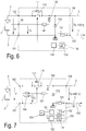
- FIG. 3 shows the structure of a protective device 100 in a further embodiment in a detailed circuit diagram.
- the same reference numerals in this as in the following figures identify the same and the same elements as in FIG. 1 ,
- the protective device 100 is connected with its inputs 101 and 102 via connection lines 2, in turn, to a PV generator 1, which is symbolized as a single photovoltaic cell. That's true FIG. 1 said in This as well as in the following embodiments, according to which it may be in the PV generator 1 to one or more, in particular series-connected PV modules.
- the protective device 100 has outputs 103 and 104. While the output 103 is permanently connected to the input 101 via a current measuring resistor (shunt) 131 in a low-impedance manner, the output 104 can be connected to the input 102 in a switchable manner via the switching element 110.
- the switching element 110 is symbolically reproduced as a controllable switch, the switching element 110 is preferably designed as a semiconductor switch, z. B. in the form of an IGBT (Insulated Gate Bipolar Transistor) or a MOSFET (Metal Oxide Semiconductor Field Effect Transistor). The switching element 110 can switch the output 104 as shown.
- both outputs 103, 104 can switch. It can also be provided, for example to increase the switching reliability, to use a plurality of switches, for example semiconductor switches, in a series connection as a switching element 110.
- a diode 111 is arranged parallel to the switching path of the switching element 110.
- the diode 111 protects a designed as a semiconductor switch switching device 110 against excessive reverse voltages that could occur when the PV generator 1 is shaded, but via the outputs 103, 104 voltage is applied, for. B. due to a capacitor in the DC input circuit of the inverter.
- the diode 111 is already integrated in the semiconductor switch due to the internal structure of the semiconductor. It is also called an intrinsic diode in such a case.
- Another diode 112 is connected in anti-parallel to the outputs 103, 104. It serves as a bypass diode for an application in which several PV generators 1 are each connected in series with their own protective circuits 100. Such a system design will also be related to FIG. 4 explained in more detail.
- the current measuring resistor 131 forms a current measuring device 130.
- a voltage which is proportional to the current Io is established in relation to a reference potential GND which is valid for the protective device 100. This is compared in the threshold value switch 132 with a voltage corresponding to a predetermined current Is.
- the output of the threshold switch 132 is supplied with a voltage when the current Io exceeds the predetermined threshold Is.
- a hysteresis in the switching process can be provided.
- a lower and an upper threshold Isu, Iso are given, which differ from each other.
- the thresholds are selected so that switching on of the switching element 110 upon contact with one of the DC lines 3 or at a greatly reduced insulation resistance of the DC lines 3 or the DC input of the inverter 4, z. B. by extinguishing water is excluded.
- the threshold switch 132 is connected to a timer 133, the output of which is then applied with a non-zero voltage, if applied to its input for longer than a predetermined period tx the non-zero signal. From the output of the timer 133, the switching member 110 is switched.
- the timer 133 precludes that short interference voltage pulses, which are induced for example in the DC lines 3, lead to switching of the switching member 110. Only when a longer than the predetermined period tx, z. B. longer than a few hundred milliseconds or a few seconds, continuous current flow lo greater Is is detected, the switching device 110 turns on, wherein optionally a further time delay is passed through before switching.
- the further time delay ensures that in the case of a plurality of protective devices 100 connected in parallel, switching on a first protection device 100 does not interrupt the current flow at the outputs 103, 104 of the further protection devices 100 before the end of the respective predetermined time period tx.
- the switching member 110 switches off immediately after falling below the switching threshold and only turns on again when the switching threshold is exceeded for longer than the predetermined period tx.
- the low voltage Us is generated via a DC-DC converter (DC / DC converter) 140 from the input voltage Ui.
- the low voltage Us is connected with its negative pole to the reference potential GND and guided with its positive pole via a series resistor 141 and a diode 142 to the output 104.
- the diode 142 prevents a backflow of current into the DC / DC converter 140, if the output 104 is applied with a voltage lying above the low voltage Us, z. B. when the switching device 110 is turned on.
- the series resistor 141 is used to limit the current flowing due to the low voltage Us.
- the series resistor 141 must not be chosen so large that a current flow greater than the threshold value Is at a given level of the low voltage Us is not reached. Of particular importance receives the series resistor 141 in connection with a plurality of interconnected, in particular parallel-connected protective devices and in connection with an arc extinguishing, as in connection with FIG. 6 is described.
- the DC / DC converter 140 may also be designed to be actively regulated in a current-limited manner.
- a voltage regulator designed as a longitudinal regulator or a transverse regulator can also be used in order to limit the input voltage Ui to the low voltage Us.
- Such regulators are simpler in construction but involve higher conversion losses.
- a diode 111 is not provided.
- the switching device 110 opens at currents lo less than or equal to the lower threshold Isu and thus also at negative currents (return currents). Without the diode 111 flows with the switching device open no reverse current through the PV generator 1.
- This functionality is particularly in a parallel circuit makes sense from several PV generators, since otherwise it can come to high reverse currents in one of the PV generators, for example, by a faulty connection or by defective bypass diodes.
- a protective circuit which prevents a reverse current can be dispensed with the hitherto used in a parallel connection of PV generators, for example, in a parallel connection of strings, fuse used when such a protection circuit is present for each of the parallel-connected PV generators.
- semiconductor switches with intrinsic diodes are used for the switching device 110, two such semiconductor switches can be bidirectionally connected in series to form a switching device 110, in which a return current is prevented when the switching device 110 is open.
- FIG. 4 shows the structure of a protective device 100 in a further embodiment in a detailed circuit diagram.
- a switching element 110 is also provided here, via one of the inputs, here the input 102, with one of the outputs, here the output 104, is connected to low resistance.
- the other input 101 is fixed to the other output 103.
- a DC / DC converter 140 is provided for generating a protective extra-low voltage Us, with which the outputs 103, 104 are applied via a series resistor 141 and a diode 142, if the switching member 110 is opened.
- the magnitude of the current I 0 output by the outputs does not represent the signal which is compared with predetermined criteria. Instead, the switching device 110 is turned on when a coded in a certain way waveform, such as a pulse train is detected, which is modulated on the voltage applied to the outputs 103, 104 DC voltage.
- the protective device 100 has for this purpose a decoding unit 134, which is supplied to the voltage applied to the outputs 103, 104 voltage Uo for evaluation.
- the decoding unit 134 monitors whether there is a voltage signal at the outputs 103, 104, which follows predetermined criteria changes over time.
- a temporal change, also called modulation can be given for example by a sequence of pulses (pulse pattern), wherein a pulse is characterized in each case by a brief voltage dip.
- pulse pattern a sequence of pulses
- the decoder unit 134 turns on the switch member 110, if not, the switch member 110 is turned off.
- the decoding unit 134 may alternatively be set up to evaluate the current Io flowing at the outputs 103, 104 to the presence of a modulated current signal.
- a modulation of the current Io can be analogous to the case of the evaluation of the output voltage Uo be given for example by a series of pulses, wherein a pulse is characterized in each case by a short increase in current.
- a corresponding signal for switching on the switching element 110 is modulated onto the DC lines 3 by a device positioned away from the protective device 100.
- the signal is repeated with the predetermined pattern, e.g. periodically modulated onto the DC lines 3, whereby they are acted upon by the voltage provided by the PV generator 1 voltage.
- the impressing of the signal with the predetermined pattern is omitted, whereupon the protective circuit 100 disconnects the low-resistance connection between the PV generator 1 and the DC lines 3 and supplies them with the harmless low voltage Us.
- This embodiment is particularly resistant to interference, since, for example, a current flow due to a short circuit or an arc is not mistakenly regarded as a signal for switching on the switching element.
- a complex pulse pattern can be selected for switching on, wherein a redundancy function can be provided so that a faulty detection of a supposed turn-on signal is minimized or virtually eliminated.
- the modulating can take place in that at least one tactile switch, which is connected to the DC lines 3, via a signal generator is controlled.
- the clockable switch can be connected in series with a load resistor between the two DC power lines 3, that is, parallel to the input terminals of an inverter and thus parallel to the terminals 103 and 104 of the protection device 100.
- a clocked switching on of the switch leads to a switch clock correspondingly modulated current signal, which also impresses a modulated voltage signal at the terminals 103 and 104 because of the non-zero internal resistance of the protective device 100.
- the internal resistance of the protective device 100 is dominated by the series resistor 141 when (still) open switching element 110.
- the tactile switch may be integrated into the inverter 4 specifically for this purpose. Such a switch would have the additional benefit that a capacitor present in an input stage of the inverter can be discharged via the series circuit of tactile switch and load resistor regardless of the operating state of the inverter, which may be desirable for safety reasons.
- an already existing switch in the inverter 4 can be used to impress the current or voltage signal, for example a switch of a DC-DC converter or another input stage of the inverter 4.
- a separate tactile switch can be used if the Inverter 4 is not yet in operation and the DC cables 3 are subjected to the low voltage Us.
- FIG. 5 shows a preferred embodiment of the invention, in which a plurality of PV generators 1 are provided, each of which a protective device 100 is associated, with which the respective PV generator 1 is connected. In such a constellation with several PV generators 1, these are also referred to as PV subgenerators 1.
- the protective devices 100 are connected in series with their outputs, and the series circuit of the protective devices 100 is connected to the inverter 4.
- a total output voltage U'o which is applied to the DC lines 3 and the input of the inverter 4, results as the sum of the voltages applied to the outputs of the protective devices 100 uo.
- the flowing current Io detected by the individual protection devices 100 is the same for all protection devices and corresponds to the current Io flowing in the DC lines 3.
- this current Io exceeds the threshold current Is, it is independently detected by each of the protection devices 100, which then turn on the corresponding switching elements 110 after the predetermined period of time tx, whereupon the electrical power provided by the respective PV generators 1 is transmitted to the inverter 4 can be.
- a single PV module as a PV subgenerator 1 and the respective protection device 100 integrated into this PV module, z. B. integrated into a junction box of the PV module to arrange.
- the maximum voltage in a PV module is below the threshold voltage of 120 V.
- a PV module is created, which, like a known PV module, which has no protective device, within a PV system z. B. can be connected in series to form a string with an inverter 4, wherein in case of danger at any point of the PV system is not a dangerous voltage.
- the junction box can also be splash-proof. In this way it can be prevented that connection lines, which lead within the PV module to the protection device 100 and where the possibly high output voltage of the PV module is applied directly, can come into contact with extinguishing water. Thus, even with PV modules whose maximum output voltage is above the specified threshold voltage of 120 V, a high level of safety in the event of danger is achieved.
- PV generators 1 in parallel with associated protective devices 100.
- the current flowing through the inverter and the DC lines 3 is distributed to the individual protection devices 100, so that an overall greater current flow from the inverter 4 must be requested to initiate the switching of the individual switching devices 110.
- the low voltages Us of the various protective devices 100 due to component tolerances of DC / DC converters 140 will not be exactly the same, could result in the parallel connection of the protective devices 100 a very uneven current distribution to the protective devices 100. This is prevented by the series resistor 141, via which the output of the DC / DC converter 140 is led to the output 104 of the protective device 100.
- FIG. 6 shows the circuit diagram of another embodiment of the protective device 100 in a representation analogous to FIG. 3 , In contrast to the embodiment of FIG. 3 Here, another input 105 is provided, which is connected to a voltage tap on the PV generator 1. The voltage tap on the PV generator 1 picks up a partial voltage of the actual output voltage.
- the tap may be implemented between two of the PV modules. If, for example, ten series-connected PV modules form the PV generator 1, the tap between the first and the second PV module can be made so that the voltage applied to the tap is uniformly irradiated across all the PV modules of the PV generator 1 tenth of the total voltage provided by the PV generator 1 voltage.
- the tapped voltage is supplied to the input 105 as a low voltage Us of the protective device 100, from where it is again applied via the series resistor 141 and the diode 142 to the output 104 of the protective device 100. Due to the illustrated interconnection, the protective device 100 can provide the low voltage Us without additional component complexity and without the losses associated with a DC / DC converter or a voltage regulator, or with a lower one of these losses.
- the provision of the low voltage Us via a voltage tap can also be carried out in an alternative embodiment if, as shown in FIG. 5, several PV subgenerators 1 are connected in series, each with its own associated protective device 100. This is particularly useful when used as PV sub-generators 1 individual PV modules and the protective device 100 is arranged in a junction box of the PV module.
- the PV cells of PV modules are often grouped into several groups, eg, three groups, with the PV cells of a group in series within the cell array.
- the terminals of the individual groups are led separately into the junction box, where they are then connected in series with each other, usually a bypass diode is provided in anti-parallel to each group.
- taps of the PV module, which carry partial voltages are already available in the junction box.
- One of these taps can be routed to the further input 105 in order to easily derive the low voltage Us from this partial voltage.
- FIG. 7 shows a further embodiment of the protective device 100 in a circuit diagram analogous to FIG. 3 .
- the protection device shown here not only serves to switch off a dangerously high DC voltage on the DC lines, but also to extinguish an arc in the current flow between the PV generator 1 and the inverter 4.
- a device for arc detection 150 which includes, for example, a bandpass filter 151 and a downstream envelope detector (envelope decoder) 152. Other methods of arc detection can also be used.
- the output of the envelope detector 152 and the output of the timer 133 are combined together via a logic AND gate 153, the input connected to the envelope detector 152 being negated.
- the output of the AND-switching element 153 controls the switching element 110.
- the switching element 110 is turned on, on the one hand, if there is a current flow lo lying above an upper threshold Iso for longer than the predetermined period tx and, on the other hand, no arc is detected , Conversely, the switching device 110 disconnects the output 104 from the input 102 when a current flow lo smaller than a lower threshold Isu is observed or when an arc is detected in the DC circuit.
- the protection circuit 100 After separation of the output 104 from the input 102 is at the outputs 103, 104 again only the low voltage Us on. In this case, due to the bias resistor 141, the protection circuit 100 does not provide enough current to sustain the arc, so that the arc is extinguished. In embodiments in which no series resistor 141 is present, the same is achieved by a then provided current limit of the DC / DC converter 140.
- FIGS. 5 to 7 illustrated embodiments on the in connection with the FIG. 3 shown embodiment in which the amount of current flow at the output of the protection circuit is used as a criterion, whether the output is supplied with the low voltage or the operating voltage of the PV generator. It can also in these remarks the example of the FIG. 4 underlying criterion of an impressed on the DC lines coded signal can be used.
Landscapes
- Engineering & Computer Science (AREA)
- Power Engineering (AREA)
- Physics & Mathematics (AREA)
- General Physics & Mathematics (AREA)
- Protection Of Static Devices (AREA)
- Inverter Devices (AREA)
- Photovoltaic Devices (AREA)
- Life Sciences & Earth Sciences (AREA)
- Sustainable Development (AREA)
- Sustainable Energy (AREA)
- Direct Current Feeding And Distribution (AREA)
Applications Claiming Priority (3)
| Application Number | Priority Date | Filing Date | Title |
|---|---|---|---|
| DE102011010172A DE102011010172A1 (de) | 2011-02-02 | 2011-02-02 | Signalerzeugender Wechselrichter und Betriebsverfahren für einen Wechselrichter |
| DE102011000737A DE102011000737B4 (de) | 2011-02-15 | 2011-02-15 | Schutzeinrichtung für eine Photovoltaikanlage, Photovoltaikmodul mit einer solchen Schutzeinrichtung sowie Betriebsverfahren für eine solche Schutzeinrichtung |
| PCT/EP2011/058049 WO2012103963A1 (de) | 2011-02-02 | 2011-05-18 | Schutzeinrichtung für eine photovoltaikanlage |
Publications (2)
| Publication Number | Publication Date |
|---|---|
| EP2671256A1 EP2671256A1 (de) | 2013-12-11 |
| EP2671256B1 true EP2671256B1 (de) | 2019-03-13 |
Family
ID=46602083
Family Applications (1)
| Application Number | Title | Priority Date | Filing Date |
|---|---|---|---|
| EP11720111.1A Active EP2671256B1 (de) | 2011-02-02 | 2011-05-18 | Schutzeinrichtung für eine photovoltaikanlage |
Country Status (8)
Families Citing this family (58)
| Publication number | Priority date | Publication date | Assignee | Title |
|---|---|---|---|---|
| US10693415B2 (en) | 2007-12-05 | 2020-06-23 | Solaredge Technologies Ltd. | Testing of a photovoltaic panel |
| US11881814B2 (en) | 2005-12-05 | 2024-01-23 | Solaredge Technologies Ltd. | Testing of a photovoltaic panel |
| US8618692B2 (en) | 2007-12-04 | 2013-12-31 | Solaredge Technologies Ltd. | Distributed power system using direct current power sources |
| US11855231B2 (en) | 2006-12-06 | 2023-12-26 | Solaredge Technologies Ltd. | Distributed power harvesting systems using DC power sources |
| US11735910B2 (en) | 2006-12-06 | 2023-08-22 | Solaredge Technologies Ltd. | Distributed power system using direct current power sources |
| US8013472B2 (en) | 2006-12-06 | 2011-09-06 | Solaredge, Ltd. | Method for distributed power harvesting using DC power sources |
| US9088178B2 (en) | 2006-12-06 | 2015-07-21 | Solaredge Technologies Ltd | Distributed power harvesting systems using DC power sources |
| US8963369B2 (en) | 2007-12-04 | 2015-02-24 | Solaredge Technologies Ltd. | Distributed power harvesting systems using DC power sources |
| US8319483B2 (en) | 2007-08-06 | 2012-11-27 | Solaredge Technologies Ltd. | Digital average input current control in power converter |
| US11569659B2 (en) | 2006-12-06 | 2023-01-31 | Solaredge Technologies Ltd. | Distributed power harvesting systems using DC power sources |
| US8473250B2 (en) | 2006-12-06 | 2013-06-25 | Solaredge, Ltd. | Monitoring of distributed power harvesting systems using DC power sources |
| US11296650B2 (en) | 2006-12-06 | 2022-04-05 | Solaredge Technologies Ltd. | System and method for protection during inverter shutdown in distributed power installations |
| US11309832B2 (en) | 2006-12-06 | 2022-04-19 | Solaredge Technologies Ltd. | Distributed power harvesting systems using DC power sources |
| US12316274B2 (en) | 2006-12-06 | 2025-05-27 | Solaredge Technologies Ltd. | Pairing of components in a direct current distributed power generation system |
| US11687112B2 (en) | 2006-12-06 | 2023-06-27 | Solaredge Technologies Ltd. | Distributed power harvesting systems using DC power sources |
| US8947194B2 (en) | 2009-05-26 | 2015-02-03 | Solaredge Technologies Ltd. | Theft detection and prevention in a power generation system |
| US8531055B2 (en) | 2006-12-06 | 2013-09-10 | Solaredge Ltd. | Safety mechanisms, wake up and shutdown methods in distributed power installations |
| US11888387B2 (en) | 2006-12-06 | 2024-01-30 | Solaredge Technologies Ltd. | Safety mechanisms, wake up and shutdown methods in distributed power installations |
| US8319471B2 (en) | 2006-12-06 | 2012-11-27 | Solaredge, Ltd. | Battery power delivery module |
| US8816535B2 (en) | 2007-10-10 | 2014-08-26 | Solaredge Technologies, Ltd. | System and method for protection during inverter shutdown in distributed power installations |
| US8384243B2 (en) | 2007-12-04 | 2013-02-26 | Solaredge Technologies Ltd. | Distributed power harvesting systems using DC power sources |
| WO2009072076A2 (en) | 2007-12-05 | 2009-06-11 | Solaredge Technologies Ltd. | Current sensing on a mosfet |
| US11264947B2 (en) | 2007-12-05 | 2022-03-01 | Solaredge Technologies Ltd. | Testing of a photovoltaic panel |
| WO2009136358A1 (en) | 2008-05-05 | 2009-11-12 | Solaredge Technologies Ltd. | Direct current power combiner |
| US10673222B2 (en) | 2010-11-09 | 2020-06-02 | Solaredge Technologies Ltd. | Arc detection and prevention in a power generation system |
| US10673229B2 (en) | 2010-11-09 | 2020-06-02 | Solaredge Technologies Ltd. | Arc detection and prevention in a power generation system |
| US10230310B2 (en) | 2016-04-05 | 2019-03-12 | Solaredge Technologies Ltd | Safety switch for photovoltaic systems |
| GB2485527B (en) | 2010-11-09 | 2012-12-19 | Solaredge Technologies Ltd | Arc detection and prevention in a power generation system |
| GB2483317B (en) | 2011-01-12 | 2012-08-22 | Solaredge Technologies Ltd | Serially connected inverters |
| US8570005B2 (en) | 2011-09-12 | 2013-10-29 | Solaredge Technologies Ltd. | Direct current link circuit |
| GB2498365A (en) | 2012-01-11 | 2013-07-17 | Solaredge Technologies Ltd | Photovoltaic module |
| GB2498790A (en) | 2012-01-30 | 2013-07-31 | Solaredge Technologies Ltd | Maximising power in a photovoltaic distributed power system |
| GB2498791A (en) | 2012-01-30 | 2013-07-31 | Solaredge Technologies Ltd | Photovoltaic panel circuitry |
| US9853565B2 (en) | 2012-01-30 | 2017-12-26 | Solaredge Technologies Ltd. | Maximized power in a photovoltaic distributed power system |
| DE102012019556A1 (de) * | 2012-10-05 | 2014-02-20 | M&S sectec GbR | Verfahren zum Betreiben einer Stromquelle und Vorrichtung zum Trennen einer Stromquelle von einem Verbraucher |
| CN102914709B (zh) * | 2012-10-09 | 2015-01-07 | 常州加伏沃新能源科技有限公司 | 基于信号回声器区分逆变器噪音和直流电弧信号的方法 |
| US10143101B2 (en) | 2013-03-12 | 2018-11-27 | Chuck McCune | PV stax—multi-function junction MF/J system |
| US9791835B2 (en) | 2013-03-12 | 2017-10-17 | Chuck McCune | PV stop potential voltage and hazard stop system |
| US9548619B2 (en) | 2013-03-14 | 2017-01-17 | Solaredge Technologies Ltd. | Method and apparatus for storing and depleting energy |
| US9571022B2 (en) | 2013-08-30 | 2017-02-14 | Abb Schweiz Ag | Electrical generator with integrated hybrid rectification system comprising active and passive rectifiers connected in series |
| US9385645B2 (en) * | 2013-08-30 | 2016-07-05 | Abb Technology Ag | Methods and systems for electrical DC generation |
| CN103616596B (zh) * | 2013-11-29 | 2017-01-18 | 华为技术有限公司 | 一种基于逆变器并网的组串异常检测方法及系统 |
| EP3251191B1 (en) | 2015-01-28 | 2020-09-16 | MARICI Holdings The Netherlands B.V. | Energy panel arrangement shutdown |
| DE102016100758A1 (de) * | 2016-01-18 | 2017-07-20 | Sma Solar Technology Ag | Trennvorrichtung für einen photovoltaischen String, Solaranlage und Betriebsverfahren für eine Solaranlage mit photovoltaischem String |
| US11018623B2 (en) | 2016-04-05 | 2021-05-25 | Solaredge Technologies Ltd. | Safety switch for photovoltaic systems |
| US11177663B2 (en) | 2016-04-05 | 2021-11-16 | Solaredge Technologies Ltd. | Chain of power devices |
| US12057807B2 (en) | 2016-04-05 | 2024-08-06 | Solaredge Technologies Ltd. | Chain of power devices |
| DE102017102771A1 (de) * | 2017-02-13 | 2018-08-16 | Sma Solar Technology Ag | Verfahren zur Bestimmung einer maximal möglichen Leistung einer PV-Anlage und PV-Anlage |
| WO2019205289A1 (zh) * | 2018-04-28 | 2019-10-31 | 北京汉能光伏投资有限公司 | 太阳能组件接线盒、太阳能系统及太阳能组件控制方法 |
| AU2019440052B2 (en) | 2019-03-29 | 2023-11-09 | Huawei Digital Power Technologies Co., Ltd. | Photovoltaic converter module string, control method, and system |
| US11190023B2 (en) | 2019-04-23 | 2021-11-30 | Delta Electronics (Shanghai) Co., Ltd. | Photovoltaic inverter system and method for controlling the same |
| US11128142B2 (en) * | 2019-04-23 | 2021-09-21 | Delta Electronics (Shanghai) Co., Ltd. | Photovoltaic power generation system and method for controlling the same |
| WO2021209101A1 (en) * | 2020-04-14 | 2021-10-21 | Aalborg Universitet | Non-invasive front-end for power electronic monitoring |
| DE102021211448A1 (de) * | 2021-10-11 | 2023-04-13 | Fraunhofer-Gesellschaft zur Förderung der angewandten Forschung eingetragener Verein | Elektronische Schaltung für ein Photovoltaik-Modul und Verfahren zum Zuschalten eines Photovoltaik-Moduls |
| US11670945B1 (en) | 2022-02-28 | 2023-06-06 | Lunar Energy, Inc. | Power optimizers in series with voltage sensors and a common reference signal |
| WO2023164209A2 (en) * | 2022-02-28 | 2023-08-31 | Lunar Energy, Inc. | Rapid shutdown |
| DE102022119559A1 (de) * | 2022-08-04 | 2024-02-15 | Sma Solar Technology Ag | Photovoltaikanlage mit sicherheitsabschaltung |
| KR20240152046A (ko) * | 2023-04-12 | 2024-10-21 | 한화솔루션 주식회사 | 안전 기능 수행 장치 및 이를 포함하는 태양광 발전 시스템 |
Family Cites Families (20)
| Publication number | Priority date | Publication date | Assignee | Title |
|---|---|---|---|---|
| JPS62126418A (ja) * | 1985-11-27 | 1987-06-08 | Toshiba Corp | 太陽光発電装置 |
| DE4041672A1 (de) * | 1990-12-22 | 1992-06-25 | Zsw | Ueberwachungseinrichtung fuer einen gleichstromkreis sowie damit ausgeruestete photovoltaische energiegewinnungsanalge |
| JPH07168638A (ja) * | 1993-12-14 | 1995-07-04 | Canon Inc | インバータ装置及びその制御方法並びに発電システム |
| JP3271730B2 (ja) * | 1994-04-28 | 2002-04-08 | キヤノン株式会社 | 発電システムの充電制御装置 |
| US6300766B1 (en) * | 1998-07-24 | 2001-10-09 | Eaton Corporation | Apparatus sensitive to arc amplitude for envelope detection of low current arcs |
| JP2000174307A (ja) * | 1998-12-01 | 2000-06-23 | Toshiba Corp | 太陽電池発電モジュール及びモジュール接続台数診断装置 |
| JP2005327259A (ja) * | 2004-04-12 | 2005-11-24 | Campus Create Co Ltd | 指示位置検出装置 |
| DE102005018173B4 (de) | 2005-04-19 | 2009-05-14 | Swiontek, Karl, Dipl.-Ing. | Schalteinrichtung zur sicheren Betriebsunterbrechung von Photovoltaikanlagen |
| WO2007010326A1 (en) * | 2005-07-20 | 2007-01-25 | Ecosol Solar Technologies, Inc. | A photovoltaic power output-utilizing device |
| DE102005061865A1 (de) | 2005-12-23 | 2007-07-05 | Robert Bosch Gmbh | Verfahren zur Erhöhung der Informationsdichte in Signalübertragungsleitungen |
| DE102006060815B4 (de) | 2006-09-21 | 2013-05-29 | Solarworld Innovations Gmbh | Solarenergieerzeugungsanlage |
| US8531055B2 (en) * | 2006-12-06 | 2013-09-10 | Solaredge Ltd. | Safety mechanisms, wake up and shutdown methods in distributed power installations |
| DE102007032605A1 (de) * | 2007-07-11 | 2009-02-05 | Robert Maier | Fotovoltaikanlage |
| DE102008004675B3 (de) * | 2007-10-12 | 2009-03-05 | Fraunhofer-Gesellschaft zur Förderung der angewandten Forschung e.V. | Steuerbare Umschaltvorrichtung für ein Solarmodul |
| DE102008003272A1 (de) | 2008-01-05 | 2009-07-09 | Hans-Hermann Hunfeld | Überwachungseinheit für Photovoltaik-Module |
| DE102008008505A1 (de) * | 2008-02-11 | 2009-08-13 | Siemens Aktiengesellschaft | PV-Teilgenerator-Anschlusskasten für eine PV-Anlage sowie PV-Anlage mit einer Vielzahl derartiger PV-Teilgenerator-Anschlusskästen |
| JP4653202B2 (ja) * | 2008-09-05 | 2011-03-16 | 日本電信電話株式会社 | 充電回路および充電方法 |
| WO2010078303A2 (en) * | 2008-12-29 | 2010-07-08 | Atonometrics, Inc. | Electrical safety shutoff system and devices for photovoltaic modules |
| DE102009022508A1 (de) | 2009-05-25 | 2010-12-09 | Eaton Industries Gmbh | Safety-Schaltanlage für Solaranlagen |
| DE102010037760B4 (de) | 2010-09-24 | 2015-05-28 | Ingenieurbüro Fred Tienken | Vorrichtung und Verfahren zur Spannungsfreischaltung elektrischer, in einem Gebäude oder Gebäudekomplex verlaufender Leitungen einer Photovoltaikanlage, Verwendung der Vorrichtung sowie System mit der Vorrichtung und einer Photovoltaikanlage |
-
2011
- 2011-05-18 CN CN201180066685.4A patent/CN103348487B/zh active Active
- 2011-05-18 WO PCT/EP2011/058049 patent/WO2012103963A1/de active Application Filing
- 2011-05-18 AU AU2011358195A patent/AU2011358195B2/en active Active
- 2011-05-18 EP EP11720111.1A patent/EP2671256B1/de active Active
- 2011-05-18 CA CA 2826430 patent/CA2826430A1/en not_active Abandoned
- 2011-07-12 JP JP2013552117A patent/JP6159259B2/ja active Active
- 2011-07-12 KR KR1020137022209A patent/KR101881494B1/ko active Active
-
2013
- 2013-08-02 US US13/957,569 patent/US9780550B2/en active Active
Non-Patent Citations (1)
| Title |
|---|
| None * |
Also Published As
| Publication number | Publication date |
|---|---|
| KR20140052940A (ko) | 2014-05-07 |
| US20130320778A1 (en) | 2013-12-05 |
| EP2671256A1 (de) | 2013-12-11 |
| AU2011358195A1 (en) | 2013-08-22 |
| JP6159259B2 (ja) | 2017-07-12 |
| JP2014509176A (ja) | 2014-04-10 |
| KR101881494B1 (ko) | 2018-08-24 |
| WO2012103963A1 (de) | 2012-08-09 |
| CA2826430A1 (en) | 2012-08-09 |
| CN103348487A (zh) | 2013-10-09 |
| WO2012103963A9 (de) | 2013-09-12 |
| CN103348487B (zh) | 2017-06-06 |
| AU2011358195B2 (en) | 2015-12-24 |
| US9780550B2 (en) | 2017-10-03 |
Similar Documents
| Publication | Publication Date | Title |
|---|---|---|
| EP2671256B1 (de) | Schutzeinrichtung für eine photovoltaikanlage | |
| DE19930122C1 (de) | Verfahren zur Verhinderung des Draufschaltens auf in Abzweigen bestehende elektrische Kurzschlüsse und zugehörige Anordnung | |
| DE102012109012B4 (de) | Schaltungsanordnung für ein Solarkraftwerk mit einer Gleichspannungsquelle für eine Offsetspannung | |
| WO2012028247A1 (de) | Verfahren und vorrichtung zum sicheren schalten einer photovoltaikanlage nach unterscheidung der lichtbogenart | |
| EP2256823A1 (de) | Anschlussdose, Solarpaneel und Verwendung des Solarpaneels | |
| WO2008110129A1 (de) | Verfahren zur schadenbegrenzung eines leistungshalbleiter aufweisenden stromrichters bei einem kurzschluss im gleichspannungszwischenkreis | |
| EP2954558A1 (de) | Sichere photovoltaik-anlage | |
| EP2296244A1 (de) | Verfahren und Schaltungsanordnung zum Verbinden mindestens eines Strings einer Photovoltaikanlage mit einem Wechselrichter | |
| DE102012112184A1 (de) | Verfahren und Vorrichtung zum Schutz mehrerer Strings eines Photovoltaikgenerators vor Rückströmen | |
| DE102010026778A1 (de) | Vorrichtung zur Bereitstellung einer Eingangsgleichspannung für einen Photovol taikwechselrichter und Photovoltaikanlage mit dieser | |
| DE202011110074U1 (de) | Modulbypassschaltung für ein Photovoltaikmodul | |
| DE102010060463B4 (de) | Schaltungsanordnung zur Potentialeinstellung eines Photovoltaikgenerators und Photovoltaikanlage | |
| EP3565074A1 (de) | Ankopplungsschaltung mit schaltender funktion zur ankopplung eines isolationsüberwachungsgerätes an ein ungeerdetes stromversorgungssystem | |
| EP3783783A1 (de) | Anordnung zum regeln eines leistungsflusses in einem wechselspannungsnetz und verfahren zum schutz der anordnung | |
| EP3516701B1 (de) | Solarmodul, photovoltaikanlage und verfahren zur spannungsbegrenzung | |
| DE102011000737B4 (de) | Schutzeinrichtung für eine Photovoltaikanlage, Photovoltaikmodul mit einer solchen Schutzeinrichtung sowie Betriebsverfahren für eine solche Schutzeinrichtung | |
| EP2456034B1 (de) | Photovoltaikanlage und Photovoltaikmodul | |
| DE102015115284B3 (de) | Schutzvorrichtung für eine elektrische Energieversorgungseinrichtung und elektrische Energieversorgungseinrichtung mit einer derartigen Schutzvorrichtung | |
| DE19736903A1 (de) | Umrichter mit Gleichspannungszwischenkreis sowie Verfahren zum Betrieb eines solchen Umrichters | |
| WO2010145682A1 (de) | Parallel zum leistungsschalter geschaltete stromversorgung für dessen steuerschaltung | |
| DE102010060399A1 (de) | Photovoltaikanlage zur Einspeisung von elektrischer Leistung in ein Energieversorgungsnetz und Verfahren zum Betreiben einer solchen Anlage | |
| DE102010004395A1 (de) | Schaltungsanordnung zum Schutz von Photovoltaikmodulen | |
| BE1024324B1 (de) | Photovoltaik-Anlage, Gleichstrom-Hybrid-Schalteinrichtung, Verwendung und Verfahren zum An-und Abschalten eines Photovoltaik-Strangs | |
| BE1024328B1 (de) | Multistrang-Photovoltaik-Anlage, Verfahren zum Betrieb einer solchen und Strangabschaltvorrichtung für eine solche | |
| DE102013112362A1 (de) | Photovoltaikanlage sowie Betriebsverfahren und Wechselrichter für eine Photovoltaikanlage |
Legal Events
| Date | Code | Title | Description |
|---|---|---|---|
| PUAI | Public reference made under article 153(3) epc to a published international application that has entered the european phase |
Free format text: ORIGINAL CODE: 0009012 |
|
| 17P | Request for examination filed |
Effective date: 20130830 |
|
| AK | Designated contracting states |
Kind code of ref document: A1 Designated state(s): AL AT BE BG CH CY CZ DE DK EE ES FI FR GB GR HR HU IE IS IT LI LT LU LV MC MK MT NL NO PL PT RO RS SE SI SK SM TR |
|
| DAX | Request for extension of the european patent (deleted) | ||
| GRAP | Despatch of communication of intention to grant a patent |
Free format text: ORIGINAL CODE: EPIDOSNIGR1 |
|
| STAA | Information on the status of an ep patent application or granted ep patent |
Free format text: STATUS: GRANT OF PATENT IS INTENDED |
|
| INTG | Intention to grant announced |
Effective date: 20181024 |
|
| GRAS | Grant fee paid |
Free format text: ORIGINAL CODE: EPIDOSNIGR3 |
|
| GRAA | (expected) grant |
Free format text: ORIGINAL CODE: 0009210 |
|
| STAA | Information on the status of an ep patent application or granted ep patent |
Free format text: STATUS: THE PATENT HAS BEEN GRANTED |
|
| RIN1 | Information on inventor provided before grant (corrected) |
Inventor name: HOPF, MARKUS Inventor name: GREIZER, FRANK Inventor name: FRIEBE, JENS Inventor name: VICTOR, MATTHIAS Inventor name: BETTENWORT, GERD |
|
| AK | Designated contracting states |
Kind code of ref document: B1 Designated state(s): AL AT BE BG CH CY CZ DE DK EE ES FI FR GB GR HR HU IE IS IT LI LT LU LV MC MK MT NL NO PL PT RO RS SE SI SK SM TR |
|
| REG | Reference to a national code |
Ref country code: GB Ref legal event code: FG4D Free format text: NOT ENGLISH |
|
| REG | Reference to a national code |
Ref country code: CH Ref legal event code: EP Ref country code: AT Ref legal event code: REF Ref document number: 1108884 Country of ref document: AT Kind code of ref document: T Effective date: 20190315 |
|
| REG | Reference to a national code |
Ref country code: IE Ref legal event code: FG4D Free format text: LANGUAGE OF EP DOCUMENT: GERMAN |
|
| REG | Reference to a national code |
Ref country code: DE Ref legal event code: R096 Ref document number: 502011015480 Country of ref document: DE |
|
| REG | Reference to a national code |
Ref country code: NL Ref legal event code: FP |
|
| REG | Reference to a national code |
Ref country code: LT Ref legal event code: MG4D |
|
| PG25 | Lapsed in a contracting state [announced via postgrant information from national office to epo] |
Ref country code: NO Free format text: LAPSE BECAUSE OF FAILURE TO SUBMIT A TRANSLATION OF THE DESCRIPTION OR TO PAY THE FEE WITHIN THE PRESCRIBED TIME-LIMIT Effective date: 20190613 Ref country code: FI Free format text: LAPSE BECAUSE OF FAILURE TO SUBMIT A TRANSLATION OF THE DESCRIPTION OR TO PAY THE FEE WITHIN THE PRESCRIBED TIME-LIMIT Effective date: 20190313 Ref country code: LT Free format text: LAPSE BECAUSE OF FAILURE TO SUBMIT A TRANSLATION OF THE DESCRIPTION OR TO PAY THE FEE WITHIN THE PRESCRIBED TIME-LIMIT Effective date: 20190313 Ref country code: SE Free format text: LAPSE BECAUSE OF FAILURE TO SUBMIT A TRANSLATION OF THE DESCRIPTION OR TO PAY THE FEE WITHIN THE PRESCRIBED TIME-LIMIT Effective date: 20190313 |
|
| PG25 | Lapsed in a contracting state [announced via postgrant information from national office to epo] |
Ref country code: BG Free format text: LAPSE BECAUSE OF FAILURE TO SUBMIT A TRANSLATION OF THE DESCRIPTION OR TO PAY THE FEE WITHIN THE PRESCRIBED TIME-LIMIT Effective date: 20190613 Ref country code: HR Free format text: LAPSE BECAUSE OF FAILURE TO SUBMIT A TRANSLATION OF THE DESCRIPTION OR TO PAY THE FEE WITHIN THE PRESCRIBED TIME-LIMIT Effective date: 20190313 Ref country code: GR Free format text: LAPSE BECAUSE OF FAILURE TO SUBMIT A TRANSLATION OF THE DESCRIPTION OR TO PAY THE FEE WITHIN THE PRESCRIBED TIME-LIMIT Effective date: 20190614 Ref country code: LV Free format text: LAPSE BECAUSE OF FAILURE TO SUBMIT A TRANSLATION OF THE DESCRIPTION OR TO PAY THE FEE WITHIN THE PRESCRIBED TIME-LIMIT Effective date: 20190313 Ref country code: RS Free format text: LAPSE BECAUSE OF FAILURE TO SUBMIT A TRANSLATION OF THE DESCRIPTION OR TO PAY THE FEE WITHIN THE PRESCRIBED TIME-LIMIT Effective date: 20190313 |
|
| PG25 | Lapsed in a contracting state [announced via postgrant information from national office to epo] |
Ref country code: CZ Free format text: LAPSE BECAUSE OF FAILURE TO SUBMIT A TRANSLATION OF THE DESCRIPTION OR TO PAY THE FEE WITHIN THE PRESCRIBED TIME-LIMIT Effective date: 20190313 Ref country code: SK Free format text: LAPSE BECAUSE OF FAILURE TO SUBMIT A TRANSLATION OF THE DESCRIPTION OR TO PAY THE FEE WITHIN THE PRESCRIBED TIME-LIMIT Effective date: 20190313 Ref country code: RO Free format text: LAPSE BECAUSE OF FAILURE TO SUBMIT A TRANSLATION OF THE DESCRIPTION OR TO PAY THE FEE WITHIN THE PRESCRIBED TIME-LIMIT Effective date: 20190313 Ref country code: ES Free format text: LAPSE BECAUSE OF FAILURE TO SUBMIT A TRANSLATION OF THE DESCRIPTION OR TO PAY THE FEE WITHIN THE PRESCRIBED TIME-LIMIT Effective date: 20190313 Ref country code: EE Free format text: LAPSE BECAUSE OF FAILURE TO SUBMIT A TRANSLATION OF THE DESCRIPTION OR TO PAY THE FEE WITHIN THE PRESCRIBED TIME-LIMIT Effective date: 20190313 Ref country code: PT Free format text: LAPSE BECAUSE OF FAILURE TO SUBMIT A TRANSLATION OF THE DESCRIPTION OR TO PAY THE FEE WITHIN THE PRESCRIBED TIME-LIMIT Effective date: 20190713 Ref country code: AL Free format text: LAPSE BECAUSE OF FAILURE TO SUBMIT A TRANSLATION OF THE DESCRIPTION OR TO PAY THE FEE WITHIN THE PRESCRIBED TIME-LIMIT Effective date: 20190313 |
|
| PG25 | Lapsed in a contracting state [announced via postgrant information from national office to epo] |
Ref country code: PL Free format text: LAPSE BECAUSE OF FAILURE TO SUBMIT A TRANSLATION OF THE DESCRIPTION OR TO PAY THE FEE WITHIN THE PRESCRIBED TIME-LIMIT Effective date: 20190313 Ref country code: SM Free format text: LAPSE BECAUSE OF FAILURE TO SUBMIT A TRANSLATION OF THE DESCRIPTION OR TO PAY THE FEE WITHIN THE PRESCRIBED TIME-LIMIT Effective date: 20190313 |
|
| REG | Reference to a national code |
Ref country code: DE Ref legal event code: R097 Ref document number: 502011015480 Country of ref document: DE |
|
| REG | Reference to a national code |
Ref country code: CH Ref legal event code: PL |
|
| PG25 | Lapsed in a contracting state [announced via postgrant information from national office to epo] |
Ref country code: IS Free format text: LAPSE BECAUSE OF FAILURE TO SUBMIT A TRANSLATION OF THE DESCRIPTION OR TO PAY THE FEE WITHIN THE PRESCRIBED TIME-LIMIT Effective date: 20190713 |
|
| PLBE | No opposition filed within time limit |
Free format text: ORIGINAL CODE: 0009261 |
|
| STAA | Information on the status of an ep patent application or granted ep patent |
Free format text: STATUS: NO OPPOSITION FILED WITHIN TIME LIMIT |
|
| PG25 | Lapsed in a contracting state [announced via postgrant information from national office to epo] |
Ref country code: MC Free format text: LAPSE BECAUSE OF FAILURE TO SUBMIT A TRANSLATION OF THE DESCRIPTION OR TO PAY THE FEE WITHIN THE PRESCRIBED TIME-LIMIT Effective date: 20190313 Ref country code: DK Free format text: LAPSE BECAUSE OF FAILURE TO SUBMIT A TRANSLATION OF THE DESCRIPTION OR TO PAY THE FEE WITHIN THE PRESCRIBED TIME-LIMIT Effective date: 20190313 Ref country code: CH Free format text: LAPSE BECAUSE OF NON-PAYMENT OF DUE FEES Effective date: 20190531 Ref country code: LI Free format text: LAPSE BECAUSE OF NON-PAYMENT OF DUE FEES Effective date: 20190531 |
|
| 26N | No opposition filed |
Effective date: 20191216 |
|
| PG25 | Lapsed in a contracting state [announced via postgrant information from national office to epo] |
Ref country code: SI Free format text: LAPSE BECAUSE OF FAILURE TO SUBMIT A TRANSLATION OF THE DESCRIPTION OR TO PAY THE FEE WITHIN THE PRESCRIBED TIME-LIMIT Effective date: 20190313 Ref country code: LU Free format text: LAPSE BECAUSE OF NON-PAYMENT OF DUE FEES Effective date: 20190518 |
|
| PG25 | Lapsed in a contracting state [announced via postgrant information from national office to epo] |
Ref country code: TR Free format text: LAPSE BECAUSE OF FAILURE TO SUBMIT A TRANSLATION OF THE DESCRIPTION OR TO PAY THE FEE WITHIN THE PRESCRIBED TIME-LIMIT Effective date: 20190313 |
|
| PG25 | Lapsed in a contracting state [announced via postgrant information from national office to epo] |
Ref country code: IE Free format text: LAPSE BECAUSE OF NON-PAYMENT OF DUE FEES Effective date: 20190518 |
|
| REG | Reference to a national code |
Ref country code: AT Ref legal event code: MM01 Ref document number: 1108884 Country of ref document: AT Kind code of ref document: T Effective date: 20190518 |
|
| PG25 | Lapsed in a contracting state [announced via postgrant information from national office to epo] |
Ref country code: AT Free format text: LAPSE BECAUSE OF NON-PAYMENT OF DUE FEES Effective date: 20190518 |
|
| PG25 | Lapsed in a contracting state [announced via postgrant information from national office to epo] |
Ref country code: CY Free format text: LAPSE BECAUSE OF FAILURE TO SUBMIT A TRANSLATION OF THE DESCRIPTION OR TO PAY THE FEE WITHIN THE PRESCRIBED TIME-LIMIT Effective date: 20190313 |
|
| PG25 | Lapsed in a contracting state [announced via postgrant information from national office to epo] |
Ref country code: MT Free format text: LAPSE BECAUSE OF FAILURE TO SUBMIT A TRANSLATION OF THE DESCRIPTION OR TO PAY THE FEE WITHIN THE PRESCRIBED TIME-LIMIT Effective date: 20190313 Ref country code: HU Free format text: LAPSE BECAUSE OF FAILURE TO SUBMIT A TRANSLATION OF THE DESCRIPTION OR TO PAY THE FEE WITHIN THE PRESCRIBED TIME-LIMIT; INVALID AB INITIO Effective date: 20110518 |
|
| PG25 | Lapsed in a contracting state [announced via postgrant information from national office to epo] |
Ref country code: MK Free format text: LAPSE BECAUSE OF FAILURE TO SUBMIT A TRANSLATION OF THE DESCRIPTION OR TO PAY THE FEE WITHIN THE PRESCRIBED TIME-LIMIT Effective date: 20190313 |
|
| P01 | Opt-out of the competence of the unified patent court (upc) registered |
Effective date: 20230614 |
|
| REG | Reference to a national code |
Ref country code: DE Ref legal event code: R079 Ref document number: 502011015480 Country of ref document: DE Free format text: PREVIOUS MAIN CLASS: H01L0031020000 Ipc: H10F0077000000 |
|
| PGFP | Annual fee paid to national office [announced via postgrant information from national office to epo] |
Ref country code: NL Payment date: 20250522 Year of fee payment: 15 |
|
| PGFP | Annual fee paid to national office [announced via postgrant information from national office to epo] |
Ref country code: DE Payment date: 20250519 Year of fee payment: 15 |
|
| PGFP | Annual fee paid to national office [announced via postgrant information from national office to epo] |
Ref country code: GB Payment date: 20250522 Year of fee payment: 15 |
|
| PGFP | Annual fee paid to national office [announced via postgrant information from national office to epo] |
Ref country code: IT Payment date: 20250530 Year of fee payment: 15 Ref country code: BE Payment date: 20250520 Year of fee payment: 15 |
|
| PGFP | Annual fee paid to national office [announced via postgrant information from national office to epo] |
Ref country code: FR Payment date: 20250521 Year of fee payment: 15 |