EP2670068B1 - Optical data transmission device using optical time domain reflectrometry - Google Patents
Optical data transmission device using optical time domain reflectrometry Download PDFInfo
- Publication number
- EP2670068B1 EP2670068B1 EP12305591.5A EP12305591A EP2670068B1 EP 2670068 B1 EP2670068 B1 EP 2670068B1 EP 12305591 A EP12305591 A EP 12305591A EP 2670068 B1 EP2670068 B1 EP 2670068B1
- Authority
- EP
- European Patent Office
- Prior art keywords
- optical
- signal
- unit
- measurement
- tia
- Prior art date
- Legal status (The legal status is an assumption and is not a legal conclusion. Google has not performed a legal analysis and makes no representation as to the accuracy of the status listed.)
- Not-in-force
Links
- 230000003287 optical effect Effects 0.000 title claims description 182
- 230000005540 biological transmission Effects 0.000 title claims description 122
- 238000005259 measurement Methods 0.000 claims description 92
- 238000000253 optical time-domain reflectometry Methods 0.000 claims description 22
- 238000000034 method Methods 0.000 claims description 9
- 230000004044 response Effects 0.000 description 8
- 230000001427 coherent effect Effects 0.000 description 6
- 239000000835 fiber Substances 0.000 description 5
- 230000001902 propagating effect Effects 0.000 description 5
- 239000013307 optical fiber Substances 0.000 description 4
- 238000012935 Averaging Methods 0.000 description 3
- 230000006870 function Effects 0.000 description 3
- 230000010354 integration Effects 0.000 description 2
- 230000021715 photosynthesis, light harvesting Effects 0.000 description 2
- 238000005311 autocorrelation function Methods 0.000 description 1
- 238000006243 chemical reaction Methods 0.000 description 1
- 239000006185 dispersion Substances 0.000 description 1
- 230000000694 effects Effects 0.000 description 1
- 238000005516 engineering process Methods 0.000 description 1
- 238000001914 filtration Methods 0.000 description 1
- 238000000691 measurement method Methods 0.000 description 1
- 238000012544 monitoring process Methods 0.000 description 1
- 239000004065 semiconductor Substances 0.000 description 1
Images

Classifications
-
- H—ELECTRICITY
- H04—ELECTRIC COMMUNICATION TECHNIQUE
- H04B—TRANSMISSION
- H04B10/00—Transmission systems employing electromagnetic waves other than radio-waves, e.g. infrared, visible or ultraviolet light, or employing corpuscular radiation, e.g. quantum communication
- H04B10/50—Transmitters
- H04B10/501—Structural aspects
- H04B10/503—Laser transmitters
-
- G—PHYSICS
- G01—MEASURING; TESTING
- G01M—TESTING STATIC OR DYNAMIC BALANCE OF MACHINES OR STRUCTURES; TESTING OF STRUCTURES OR APPARATUS, NOT OTHERWISE PROVIDED FOR
- G01M11/00—Testing of optical apparatus; Testing structures by optical methods not otherwise provided for
-
- G—PHYSICS
- G01—MEASURING; TESTING
- G01M—TESTING STATIC OR DYNAMIC BALANCE OF MACHINES OR STRUCTURES; TESTING OF STRUCTURES OR APPARATUS, NOT OTHERWISE PROVIDED FOR
- G01M11/00—Testing of optical apparatus; Testing structures by optical methods not otherwise provided for
- G01M11/30—Testing of optical devices, constituted by fibre optics or optical waveguides
- G01M11/31—Testing of optical devices, constituted by fibre optics or optical waveguides with a light emitter and a light receiver being disposed at the same side of a fibre or waveguide end-face, e.g. reflectometers
- G01M11/3109—Reflectometers detecting the back-scattered light in the time-domain, e.g. OTDR
- G01M11/3118—Reflectometers detecting the back-scattered light in the time-domain, e.g. OTDR using coded light-pulse sequences
-
- G—PHYSICS
- G01—MEASURING; TESTING
- G01M—TESTING STATIC OR DYNAMIC BALANCE OF MACHINES OR STRUCTURES; TESTING OF STRUCTURES OR APPARATUS, NOT OTHERWISE PROVIDED FOR
- G01M11/00—Testing of optical apparatus; Testing structures by optical methods not otherwise provided for
- G01M11/30—Testing of optical devices, constituted by fibre optics or optical waveguides
- G01M11/31—Testing of optical devices, constituted by fibre optics or optical waveguides with a light emitter and a light receiver being disposed at the same side of a fibre or waveguide end-face, e.g. reflectometers
- G01M11/3109—Reflectometers detecting the back-scattered light in the time-domain, e.g. OTDR
- G01M11/3127—Reflectometers detecting the back-scattered light in the time-domain, e.g. OTDR using multiple or wavelength variable input source
-
- H—ELECTRICITY
- H04—ELECTRIC COMMUNICATION TECHNIQUE
- H04B—TRANSMISSION
- H04B10/00—Transmission systems employing electromagnetic waves other than radio-waves, e.g. infrared, visible or ultraviolet light, or employing corpuscular radiation, e.g. quantum communication
- H04B10/07—Arrangements for monitoring or testing transmission systems; Arrangements for fault measurement of transmission systems
- H04B10/071—Arrangements for monitoring or testing transmission systems; Arrangements for fault measurement of transmission systems using a reflected signal, e.g. using optical time domain reflectometers [OTDR]
-
- H—ELECTRICITY
- H04—ELECTRIC COMMUNICATION TECHNIQUE
- H04B—TRANSMISSION
- H04B10/00—Transmission systems employing electromagnetic waves other than radio-waves, e.g. infrared, visible or ultraviolet light, or employing corpuscular radiation, e.g. quantum communication
- H04B10/07—Arrangements for monitoring or testing transmission systems; Arrangements for fault measurement of transmission systems
- H04B10/075—Arrangements for monitoring or testing transmission systems; Arrangements for fault measurement of transmission systems using an in-service signal
- H04B10/079—Arrangements for monitoring or testing transmission systems; Arrangements for fault measurement of transmission systems using an in-service signal using measurements of the data signal
-
- H—ELECTRICITY
- H04—ELECTRIC COMMUNICATION TECHNIQUE
- H04B—TRANSMISSION
- H04B10/00—Transmission systems employing electromagnetic waves other than radio-waves, e.g. infrared, visible or ultraviolet light, or employing corpuscular radiation, e.g. quantum communication
- H04B10/50—Transmitters
Definitions
- the invention relates to the field of telecommunications, and in particular to a device of and a method for optical data transmission in an optical access network.
- access networks also called passive optical networks (PON) are used, for connecting a plurality of customers to a core network of data transportation.
- PON passive optical networks
- the interconnection between the core network and the access network is given at a so-called central office, which contains an optical line terminal (OLT).
- OLT optical line terminal
- the OLT is connected via at least one optical fiber, preferably called optical feeder fiber, to a so-called remote node.
- an optical downlink signal transmitted by the OLT is split onto different optical branches, to which one or more customers are connected by means of optical network units (ONU).
- ONU optical network units
- the customers send via the optical branches optical uplink signals towards the remote node, which combines these optical uplink signals to a combined uplink signal and transmits this via the optical feeder fiber to the optical line terminal.
- a measurement technique of optical time domain reflectometry can be applied.
- OTDR optical time domain reflectometry
- a reflection profile of the transmission channel is estimated.
- the technique of OTDR is carried out at the OLT.
- a measurement signal in the form of an optical pulse may be transmitted into the optical channel.
- the received response signal which is reflected by the optical channel, can then be traced in the time domain, for determining the reflection profile.
- a measurement signal may be generated as an optical signal carrying a correlation sequence.
- the received response signal is then recorded and used for determining the reflection profile.
- the reflection profile can be determined, by correlating a sampled version of the received response signal with the initial correlation sequence itself.
- the auto-correlation function of the correlation sequence is equal to or approximated by the dirac delta function, the result of the correlation yields an estimate of the impulse response of the optical channel in the time domain, which is an approximation of the reflection profile.
- the transmission device and the separate OTDR device are in this case both coupled to the same optical channel, preferably via an optical coupler.
- the optical channel is preferably an optical fiber connected to the devices.
- a more advanced technique is that of embedded OTDR, in which the transmission device itself contains the hardware for generating the optical transmission signal as well as the hardware that is necessary for carrying out an OTDR measurement.
- the optical transmission signal is directly modulated in dependence on a correlation sequence, wherein the frequency of this direct modulation is chosen such that it does not disturb data reception at a receiving side.
- the response signal of the optical channel can be obtained, by filtering out from received optical signal that frequency, at which the optical transmission signal was modulated.
- This received response signal can then be used for determining a reflection profile via the technique of signal correlation as it has been described previously above.
- WO2011/123687A1 discloses an optical time domain reflectometry system that can be operated, such that different modes of OTDR measurement are controlled by an external control unit.
- the device comprises a laser transmission unit, which is operable to generate an optical transmission signal. Furthermore, the device comprises a driving unit, which is operable to control the laser transmission unit, such that the optical transmission signal is modulated in dependence on a data signal, which is preferably an electrical data signal. Furthermore, the device comprises an optical reception unit, which is adapted to convert at least a fraction of a received optical signal into an electrical measurement signal. For this conversion, the optical reception unit contains and makes use of a photo-diode and an electrical amplifier, which are both an integral part of the optical reception unit. The optical reception unit is furthermore separate from the laser transmission unit in the sense, that the optical reception unit and the laser transmission unit have respective casings that are not directly connected to each other.
- the device comprises furthermore at least one control unit, which is operable to control the laser transmission unit, such that the optical transmission signal is modulated in dependence on a measurement signal.
- the control unit is furthermore operable to measure multiple electrical measurement signals during a measurement interval and to determine an averaged received electrical measurement signal based on the measured electrical signals.
- control unit is operable to control the electrical amplifier, such that the electrical amplifier is turned off during at least a fraction of a time interval, which is prior to the measurement interval, and such that the electrical amplifier is turned on during the measurement interval, and such that thermal heat generated by the electrical amplifier dissipates from the optical reception unit to the laser transmission unit for causing a temperature change at the laser transmission unit and a change of a center wavelength of the optical transmission signal (OS) generated by the laser transmission unit.
- OS optical transmission signal
- this optical signal may have a fixed wavelength with a narrow line width, preferably called bandwidth.
- the wavelength is fixed, in the sense that for a given constant temperature of the laser transmission unit also the wavelength is constant.
- the proposed device has the advantage, that no extra thermoelectric cooler or thermoelectric heater has to be foreseen within or directly at the laser transmission unit for changing the temperature in order to change the center wavelength of the generated optical signal. Instead, the thermal energy of the electrical amplifier can be used for this. This allows a higher degree of integration within the optical transmission device. Since the electrical amplifier is already present anyway within the optical reception unit for converting the received optical signal into an electrical measurement signal, no extra component has to be foreseen within the optical transmission device for generating thermal energy in order to cause a temperature change of the laser transmission unit for achieving a change of the center wavelength. All that has to be foreseen is, that the control unit is operable to turn the amplifier off during a time interval prior to the measurement interval.
- Figure 1 shows an optical transmission device OTD, which is preferably used within an optical line terminal of an optical access network.
- the device OTD contains a laser transmission unit LD, which is preferably a laser diode.
- the laser transmission unit LD is a semiconductor laser, which may be in a preferred embodiment a distributed feedback (DFB) laser.
- the transmission unit LD generates an optical signal OS, which has a center wavelength and a line width.
- the optical signal OS is transmitted into an optical sub assembly OSA.
- the optical signal OS passes an optical isolator I as well as an optically partially transmitting device M and an optical filter F towards an optical interface OIF, at which preferably a lens L is located.
- the optical interface OIF may contain a plug for connecting an optical fiber, or as an even further alternative a so call fiber pigtail.
- the optical isolator I transmits optical signals propagating from the transmission unit LD towards the lens L, while it suppresses a transmission of optical signals propagating from the lens L towards the transmission unit LD.
- the optically partially transmitting device M is preferably an optically partially reflecting mirror, which allows a greater fraction of the signal OS to propagate in the direction from the transmission unit LD towards the lens L, while it reflects a smaller fraction of the signal OS propagating in this direction. Furthermore, this mirror allows a greater fraction of an optical signal to propagate from the lens L towards the transmission unit LD, while it reflects a smaller fraction of such a signal propagating in this direction. As an example, 90 % of the energy of an optical signal are transmitted by the optically partially reflecting mirror, while 10 % of the energy of an optical signal are reflected by the optically partially reflecting mirror.
- the optically partially transmitting device M is alternatively an optical wavelength division multiplex (WDM) tap coupler.
- WDM optical wavelength division multiplex
- Such a tap coupler transmits optical signals in the direction of the optical signal OS for first predefined wavelength or wavelength range, while it suppresses transmission optical signals in this direction for a second predefined wavelength or wavelength range.
- the first predefined wavelength is coincident with the wavelength of the optical signal OS.
- the tap coupler transmits optical signals in the direction from the lens L towards the transmission unit LD for the second wavelength or wavelength range, while it directs optical signals coming from the lens L towards the reception unit ORX for the first predefined wavelength or wavelength range.
- the optical filter F allows optical signals to propagate from the transmission unit LD towards the lens L.
- the filter F filters optical signals propagating from the lens L towards the filter F in the way, that optical signals having the wavelength of the transmitted optical signal OS pass the filter F towards the optically partially transmitting device M, while optical signals of a different wavelength are reflected by the filter F towards an optical data reception unit ODRX.
- the optical transmission signal OS is a downlink signal with a wavelength of 1490 nm
- an optical uplink signal OUS which is preferably a combined uplink signal, received at the device OTD, preferably from other units of a network, has a wavelength of 1310 nm.
- the optical transmission device OTD is connectable at the lens L to an optical fiber OF, into which the device OTD transmits the transmission signal OS and receives the optical uplink signal OUS.
- the lens L can be seen as an optical interface of the device OTD.
- the laser transmission unit LD is controlled by a driving unit LDU, such that the optical transmission signal OS is modulated in dependence on an electrical data signal.
- the electrical data signal is preferably received at the device OTD via a data interface DTX.
- the control unit OC controls the laser transmission unit, LD, such that the optical transmission signal OS is modulated in dependence on a measurement signal.
- the measurement signal is preferably a digital electrical signal representing a correlation sequence.
- the laser driving unit LDU provides an electrical bias signal to the transmission unit LD for power adjustment as well as an electrical modulation signal for modulating the optical signal OS in dependence on digital data received at the driving unit LDU.
- This data is preferably received at the device OTD via a data interface DTX.
- the laser driver LDU itself is controlled by a control unit MC, which is preferably a micro controller, wherein the unit MC controls a working point of the driving unit LDU. Furthermore, the unit MC controls the driving unit LDU, such that temperature compensation is carried out.
- a control unit MC which is preferably a micro controller, wherein the unit MC controls a working point of the driving unit LDU. Furthermore, the unit MC controls the driving unit LDU, such that temperature compensation is carried out.
- the modulation of the transmission signal OS in dependence on the measurement signal is preferably carried out, by using as a correlation sequence a pseudo-random bit sequence.
- This bit sequence has a pre-defined bit rate, which is preferably a bit rate of 10 MHz.
- the bit sequence has preferably a length of 2 11 -1.
- the device OTD receives from the fiber OF at the lens L a response signal ROS of the optical channel. This signal ROS then passes the optical filter F. A fraction FROS1 of this signal ROS is reflected or suppressed by the optically partially transmitting device M towards an optical reception unit ORX. A remaining fraction FROS2 of the signal ROS is transmitted by the optically partially transmitting device M towards the isolator I, which suppresses this remaining fraction FROS2, such that it does not reach the laser unit LD.
- the signal fraction FROS1 has a wavelength that is coincident with the first predefined wavelength or wavelength range, while the signal fraction FROS 2 has wavelength that is coincident with the second predefined wavelength or wavelength range.
- the laser transmission unit LD is controlled by a control unit OC, such that the transmission signal OS is modulated in dependence on a measurement signal.
- the fraction FROS1 of the received optical signal is converted into an electrical measurement signal EMS.
- the reception unit ORX contains a photo diode PD, which converts the signal fraction FROS1 into an electrical signal, as well an amplifier TIA, which amplifies the converted electrical signal for obtaining the electrical measurement signal EMS.
- the amplifier TIA is preferably a transimpedance amplifier.
- the amplifier TIA uses preferably electrical energy provided by a power supply PS.
- the modulation of the transmission signal OS in dependence on the measurement signal is preferably an amplitude modulation.
- the modulation of the optical signal OS in dependence on the received data is also an amplitude modulation at a predefined bit rate using on and off keying. This on and off keying is preferably carried out at a bit rate of 2.5 Gigabits per second.
- the amplitude, by which the optical signal OS is modulated in dependence on the measurement signal is preferably within the range of 5 to 10 % of the optical signal's OS maximal amplitude.
- the measurement signal is modulated onto the optical signal OS successively multiple times.
- the optical reception unit ORX thus measures multiple electrical measurement signals, by converting a fraction of the received optical signal FROS1 to these respective electrical measurement signals.
- the multiple electrical measurement signals are then provided to an OTDR control unit OC, which stores these multiple electrical measurement signals and determines an average received electrical measurement signal based on the measured electrical signals.
- This averaging may be an unweighted or a weighted averaging.
- the averaged received electrical measurement signal determined within the control unit OC may then be provided via a data bus I2C to a device, not explicitly shown in Figure 1 .
- a device may the correlate the averaged measurement signal with the correlation sequence itself for finally determining a reflection profile of the optical channel.
- this correlation may be carried out directly within the control unit OC.
- the control unit MC controls the amplifier TIA, such that the amplifier TIA is turned off during at least a fraction of a time interval prior to the measurement interval.
- control unit MC is connected to a power supply PS of the amplifier TIA via an electrical connection.
- control unit MC sends an electrical control signal CS, also shown as "TIA enable", to the power supply PS.
- CS electrical control signal
- the amplifier TIA is turned on and off in dependence on the control signal CS sent by the control unit MC.
- control unit MC is connected electrically directly with the amplifier TIA, wherein the amplifier TIA provides an interface, preferably a PIN-connection not explicitly shown in Figure 1 , at which an electrical control signal can turn the amplifier TIA directly on and off.
- the amplifier TIA will generate thermal energy when it is turned on.
- the amount of thermal energy present within the reception unit ORX can be varied.
- the thermal energy present within the reception unit ORX may dissipate from the reception unit ORX towards the separate laser transmission unit LD.
- the amount of thermal energy present within the transmission unit LD due to thermal energy dissipation can be varied.
- a change or variation of the center wavelength of the optical transmission signal generated by the transmission unit LD can be achieved.
- the reception unit ORX and the laser transmission unit LD are separate in the sense, that they have respective casings that are not directly connected to each other. These casing may preferably be indirectly connected to each other via a casing of an optical sub assembly (OSA), which will be described in detail further below.
- OSA optical sub assembly
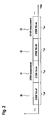
- Figure 2 shows different time intervals of measurement and non-measurement.
- the amplifier for measuring the electrical measurement signals within the reception unit has to be turned on only during such time intervals, during which a measurement of the reflection profile shall be carried out.
- the amplifier is turned on.
- the time interval I0 of non-measurement no OTDR measurement is to be performed, and thus the amplifier is turned off during this time interval of non-measurement.
- the amplifier does not have to be turned off during the whole time interval I0, but may preferably be turned off only during a fraction the time interval I0 of non-measurement.
- a number of 2 18 correlation sequences are transmitted, such that an averaged electrical measurement signal is based on 2 18 individual electrical measurement sequences.
- the time interval I1 of measurement is followed by another time interval 12 of non-measurement, which then is followed by a further time interval I3 of measurement.
- control unit controls the amplifier, such that it is turned off during at least a fraction of the time interval I2.
- the amplifier is turned on under control of the control unit.
- the turning on and off of the amplifier TIA during the respective time intervals may be carried out by a software task running on the control unit MC.
- control unit MC is preferably a micro controller
- control unit OC is preferably implemented as an application specific integrated circuit (ASIC).
- ASIC application specific integrated circuit
- control units MC and OC may be provided as separate control units or alternatively as one control unit.
- the control units OC und MC may be implemented as a common control unit or separate control units relying on different combinations of hardware and/or software.
- the optical subassembly OSA is optically connected to the laser transmission unit LD and the optical reception unit ORX.
- the optical subassembly OSA is able to provide the optical transmission signal OF to an optical interface OIF, preferably given by the lens L.
- optical subassembly OSA is able to receive the received optical signal ROF from the optical interface OIF.
- the optical subassembly OSA is preferably a hermetically sealed device with a casing CA. To this casing, the transmission unit LD and the reception unit ORX are mechanically connected. Furthermore, also an optical data reception unit ODRX is mechanically connected to the subassembly OSA.
- the optical sub-assembly may have a casing CA made of plastic.
- the casing CA of the subassembly OSA is a metallic casing, which provides the advantage of allowing a faster thermal energy dissipation from the reception unit ORX towards the transmission unit LD. This is especially of advantage in the case, that the reception unit ORX and the transmission unit LD are both sealed in respective metallic cases CA1, CA2, which are welded to the casing CA of the subassembly OSA.
- the transmission unit OTD contains preferably the optical data reception unit ODRX, which receives data via the uplink signals OUS.
- the optical data reception unit ODRX may also make use of a photo diode as well as an amplifier for deriving from the optical uplink signal OUS received data, which then may be provided to a data interface DRX.
- the proposed device discloses also a method of optical data transmission, as claimed in an independent claim, which comprises different steps corresponding to the independent claim claiming the proposed device.
- control unit' may be provided through the use of dedicated hardware as well as hardware capable of executing software in association with appropriate software.
- the functions may be provided by a single dedicated processor, by a single shared processor, or by a plurality of individual processors, some of which may be shared.
- explicit use of the term 'control unit' should not be construed to refer exclusively to hardware capable of executing software, and may implicitly include, without limitation, digital signal processor (DSP) hardware, application specific integrated circuit (ASIC), field programmable gate array (FPGA), read only memory (ROM) for storing software, random access memory (RAM), and non volatile storage.
- DSP digital signal processor
- ASIC application specific integrated circuit
- FPGA field programmable gate array
- ROM read only memory
- RAM random access memory
- non volatile storage Other hardware, conventional and/or custom, may also be included.
Landscapes
- Physics & Mathematics (AREA)
- Electromagnetism (AREA)
- Engineering & Computer Science (AREA)
- Computer Networks & Wireless Communication (AREA)
- Signal Processing (AREA)
- Optics & Photonics (AREA)
- Chemical & Material Sciences (AREA)
- Analytical Chemistry (AREA)
- General Physics & Mathematics (AREA)
- Optical Communication System (AREA)
- Light Receiving Elements (AREA)
Priority Applications (8)
| Application Number | Priority Date | Filing Date | Title |
|---|---|---|---|
| EP12305591.5A EP2670068B1 (en) | 2012-05-29 | 2012-05-29 | Optical data transmission device using optical time domain reflectrometry |
| CN201380027942.2A CN104350371B (zh) | 2012-05-29 | 2013-04-19 | 使用光时域反射计的光数据传输设备 |
| JP2015514392A JP5977445B2 (ja) | 2012-05-29 | 2013-04-19 | 光データ伝送装置 |
| KR1020147036329A KR101562159B1 (ko) | 2012-05-29 | 2013-04-19 | 광학 시간 도메인 반사측정법을 이용한 광학 데이터 송신 디바이스 |
| US14/399,330 US9287989B2 (en) | 2012-05-29 | 2013-04-19 | Optical data transmission device |
| PCT/EP2013/058132 WO2013178403A1 (en) | 2012-05-29 | 2013-04-19 | Optical data transmission device using optical time domain reflectrometry |
| IN9435DEN2014 IN2014DN09435A (enExample) | 2012-05-29 | 2013-04-19 | |
| TW102115442A TWI508470B (zh) | 2012-05-29 | 2013-04-30 | 光學資料傳輸裝置 |
Applications Claiming Priority (1)
| Application Number | Priority Date | Filing Date | Title |
|---|---|---|---|
| EP12305591.5A EP2670068B1 (en) | 2012-05-29 | 2012-05-29 | Optical data transmission device using optical time domain reflectrometry |
Publications (2)
| Publication Number | Publication Date |
|---|---|
| EP2670068A1 EP2670068A1 (en) | 2013-12-04 |
| EP2670068B1 true EP2670068B1 (en) | 2015-11-18 |
Family
ID=48141991
Family Applications (1)
| Application Number | Title | Priority Date | Filing Date |
|---|---|---|---|
| EP12305591.5A Not-in-force EP2670068B1 (en) | 2012-05-29 | 2012-05-29 | Optical data transmission device using optical time domain reflectrometry |
Country Status (8)
| Country | Link |
|---|---|
| US (1) | US9287989B2 (enExample) |
| EP (1) | EP2670068B1 (enExample) |
| JP (1) | JP5977445B2 (enExample) |
| KR (1) | KR101562159B1 (enExample) |
| CN (1) | CN104350371B (enExample) |
| IN (1) | IN2014DN09435A (enExample) |
| TW (1) | TWI508470B (enExample) |
| WO (1) | WO2013178403A1 (enExample) |
Families Citing this family (5)
| Publication number | Priority date | Publication date | Assignee | Title |
|---|---|---|---|---|
| EP2983310B1 (en) | 2014-08-05 | 2018-10-10 | Alcatel Lucent | Device and method for use in optical time domain reflectometry measurements |
| CN105024750A (zh) * | 2015-07-23 | 2015-11-04 | 常州市开拓科联通信设备有限公司 | 多功能ftth专用otdr测试仪 |
| CN107979411B (zh) * | 2016-10-21 | 2022-06-21 | 中兴通讯股份有限公司 | 一种光纤链路的监测方法及装置 |
| CN112204369B (zh) * | 2018-05-29 | 2022-11-18 | 住友电气工业株式会社 | 用于测量光纤的传输损耗的方法以及otdr测量装置 |
| US20240068905A1 (en) * | 2022-08-25 | 2024-02-29 | Ii-Vi Delaware, Inc. | Pluggable Optical Time Domain Reflectometer |
Family Cites Families (13)
| Publication number | Priority date | Publication date | Assignee | Title |
|---|---|---|---|---|
| JP2001305017A (ja) * | 2000-04-21 | 2001-10-31 | Ando Electric Co Ltd | 光パルス試験器 |
| EP1763158B1 (en) | 2005-09-12 | 2008-02-13 | Alcatel Lucent | Optical transceiver module for monitoring an optical fiber and method for making available measuring data from monitoring an optical fiber |
| KR100663462B1 (ko) | 2005-11-23 | 2007-01-02 | 삼성전자주식회사 | 수동형 광 가입자 망 |
| US20070154215A1 (en) * | 2006-01-05 | 2007-07-05 | Tellabs Bedford, Inc. | Method and apparatus for detecting optical reflections in an optical network |
| KR100912544B1 (ko) | 2006-12-01 | 2009-08-18 | 한국전자통신연구원 | 루프백방식의 파장분할다중방식 수동형 광가입자 시스템 |
| JP2008232849A (ja) * | 2007-03-20 | 2008-10-02 | Anritsu Corp | 光ファイバ監視方法及び光ファイバ監視システム |
| DE602007004951D1 (de) * | 2007-04-26 | 2010-04-08 | Alcatel Lucent | Optisches Netzwerk, Überwachungseinheit und Überwachungsverfahren |
| JP5280256B2 (ja) * | 2009-03-12 | 2013-09-04 | 住友電工デバイス・イノベーション株式会社 | 電子回路 |
| KR101033482B1 (ko) | 2009-05-11 | 2011-05-12 | 정병직 | 광선로 감시 네트워크 시스템 |
| KR101053169B1 (ko) | 2009-07-21 | 2011-08-01 | 주식회사 오이솔루션 | SiOB를 이용한 TO CAN 평행광 패키지 |
| US8854609B2 (en) * | 2010-03-31 | 2014-10-07 | Ultra Communications, Inc. | Integrated optical time domain reflectometer |
| JP5582942B2 (ja) * | 2010-09-28 | 2014-09-03 | 矢崎総業株式会社 | 信号伝送装置 |
| CN102412902B (zh) * | 2011-11-17 | 2015-12-09 | 青岛海信宽带多媒体技术有限公司 | 带光时域反射功能的光网络单元光电器件 |
-
2012
- 2012-05-29 EP EP12305591.5A patent/EP2670068B1/en not_active Not-in-force
-
2013
- 2013-04-19 KR KR1020147036329A patent/KR101562159B1/ko not_active Expired - Fee Related
- 2013-04-19 WO PCT/EP2013/058132 patent/WO2013178403A1/en not_active Ceased
- 2013-04-19 IN IN9435DEN2014 patent/IN2014DN09435A/en unknown
- 2013-04-19 CN CN201380027942.2A patent/CN104350371B/zh not_active Expired - Fee Related
- 2013-04-19 JP JP2015514392A patent/JP5977445B2/ja not_active Expired - Fee Related
- 2013-04-19 US US14/399,330 patent/US9287989B2/en not_active Expired - Fee Related
- 2013-04-30 TW TW102115442A patent/TWI508470B/zh not_active IP Right Cessation
Also Published As
| Publication number | Publication date |
|---|---|
| TW201407978A (zh) | 2014-02-16 |
| EP2670068A1 (en) | 2013-12-04 |
| IN2014DN09435A (enExample) | 2015-07-17 |
| CN104350371A (zh) | 2015-02-11 |
| KR101562159B1 (ko) | 2015-10-20 |
| TWI508470B (zh) | 2015-11-11 |
| KR20150013901A (ko) | 2015-02-05 |
| CN104350371B (zh) | 2017-05-24 |
| US9287989B2 (en) | 2016-03-15 |
| US20150117854A1 (en) | 2015-04-30 |
| JP2015525509A (ja) | 2015-09-03 |
| JP5977445B2 (ja) | 2016-08-24 |
| WO2013178403A1 (en) | 2013-12-05 |
Similar Documents
| Publication | Publication Date | Title |
|---|---|---|
| US9843397B2 (en) | Wavelength stabilizer for TWDM-PON burst mode DBR laser | |
| JP5689424B2 (ja) | Wdm−ponにおける波長アラインメントのための方法および装置 | |
| CN102771066B (zh) | 用于控制可调谐激光器的激射波长的设备及方法以及包括该设备的波分复用无源光网络 | |
| EP2670068B1 (en) | Optical data transmission device using optical time domain reflectrometry | |
| EP2731211B1 (en) | Self-seeding fiber laser device and driving method thereof, passive optical network system and device | |
| WO2012119391A1 (zh) | 可调激光器、光模块和无源光网络系统 | |
| US9106050B2 (en) | Self-characterization tunable optical network unit | |
| KR100918390B1 (ko) | 외부의 룩업 테이블을 이용한 파장 초기화 방법 및 이를사용한 파장 가변형 광송수신 장치 | |
| WO2013097183A1 (zh) | 可调激光器波长初始化方法、装置和系统 | |
| US20100322624A1 (en) | Bidirectional transmission network apparatus based on tunable rare-earth-doped fiber laser | |
| US9166691B2 (en) | Method for coupling an emitting device to a frequency splitter in an optical passive network | |
| CN102013925A (zh) | 光纤网络终端装置及其操作方法 | |
| Pöhlmann et al. | Low cost TWDM by wavelength-set division multiplexing | |
| CN105580222A (zh) | 光发射系统 | |
| JP6842869B2 (ja) | 局側終端装置 | |
| KR20090038992A (ko) | Wdm-pon 광 송신기의 구동 전류 제어 시스템 | |
| Grobe | Access networks based on tunable transmitters | |
| CN121702693A (zh) | 一种识别方法、识别装置及存储介质 | |
| KR20110129080A (ko) | 페브리-페롯 필터를 이용한 광대역 광원 | |
| JP2008263300A (ja) | 加入者側終端装置 | |
| Le et al. | Experimental demonstration of a 40 Gb/s DWDM metropolitan network over 90-km-long based on self-seeded RSOAs |
Legal Events
| Date | Code | Title | Description |
|---|---|---|---|
| PUAI | Public reference made under article 153(3) epc to a published international application that has entered the european phase |
Free format text: ORIGINAL CODE: 0009012 |
|
| 17P | Request for examination filed |
Effective date: 20121213 |
|
| AK | Designated contracting states |
Kind code of ref document: A1 Designated state(s): AL AT BE BG CH CY CZ DE DK EE ES FI FR GB GR HR HU IE IS IT LI LT LU LV MC MK MT NL NO PL PT RO RS SE SI SK SM TR |
|
| AX | Request for extension of the european patent |
Extension state: BA ME |
|
| 111Z | Information provided on other rights and legal means of execution |
Free format text: AL AT BE BG CH CY CZ DE DK EE ES FI FR GB GR HR HU IE IS IT LI LT LU LV MC MK MT NL NO PL PT RO RS SE SI SK SM TR Effective date: 20140303 |
|
| 17Q | First examination report despatched |
Effective date: 20140616 |
|
| RBV | Designated contracting states (corrected) |
Designated state(s): AL AT BE BG CH CY CZ DE DK EE ES FI FR GB GR HR HU IE IS IT LI LT LU LV MC MK MT NL NO PL PT RO RS SE SI SK SM TR |
|
| RAP1 | Party data changed (applicant data changed or rights of an application transferred) |
Owner name: ALCATEL LUCENT |
|
| D11X | Information provided on other rights and legal means of execution (deleted) | ||
| RIC1 | Information provided on ipc code assigned before grant |
Ipc: H04B 10/071 20130101AFI20150424BHEP Ipc: G01M 11/00 20060101ALI20150424BHEP |
|
| GRAP | Despatch of communication of intention to grant a patent |
Free format text: ORIGINAL CODE: EPIDOSNIGR1 |
|
| INTG | Intention to grant announced |
Effective date: 20150706 |
|
| GRAS | Grant fee paid |
Free format text: ORIGINAL CODE: EPIDOSNIGR3 |
|
| GRAA | (expected) grant |
Free format text: ORIGINAL CODE: 0009210 |
|
| AK | Designated contracting states |
Kind code of ref document: B1 Designated state(s): AL AT BE BG CH CY CZ DE DK EE ES FI FR GB GR HR HU IE IS IT LI LT LU LV MC MK MT NL NO PL PT RO RS SE SI SK SM TR |
|
| REG | Reference to a national code |
Ref country code: GB Ref legal event code: FG4D |
|
| REG | Reference to a national code |
Ref country code: CH Ref legal event code: EP |
|
| REG | Reference to a national code |
Ref country code: AT Ref legal event code: REF Ref document number: 762003 Country of ref document: AT Kind code of ref document: T Effective date: 20151215 |
|
| REG | Reference to a national code |
Ref country code: IE Ref legal event code: FG4D |
|
| REG | Reference to a national code |
Ref country code: DE Ref legal event code: R096 Ref document number: 602012012337 Country of ref document: DE |
|
| REG | Reference to a national code |
Ref country code: NL Ref legal event code: MP Effective date: 20160218 |
|
| REG | Reference to a national code |
Ref country code: LT Ref legal event code: MG4D |
|
| REG | Reference to a national code |
Ref country code: AT Ref legal event code: MK05 Ref document number: 762003 Country of ref document: AT Kind code of ref document: T Effective date: 20151118 |
|
| PG25 | Lapsed in a contracting state [announced via postgrant information from national office to epo] |
Ref country code: IT Free format text: LAPSE BECAUSE OF FAILURE TO SUBMIT A TRANSLATION OF THE DESCRIPTION OR TO PAY THE FEE WITHIN THE PRESCRIBED TIME-LIMIT Effective date: 20151118 Ref country code: NL Free format text: LAPSE BECAUSE OF FAILURE TO SUBMIT A TRANSLATION OF THE DESCRIPTION OR TO PAY THE FEE WITHIN THE PRESCRIBED TIME-LIMIT Effective date: 20151118 Ref country code: LT Free format text: LAPSE BECAUSE OF FAILURE TO SUBMIT A TRANSLATION OF THE DESCRIPTION OR TO PAY THE FEE WITHIN THE PRESCRIBED TIME-LIMIT Effective date: 20151118 Ref country code: NO Free format text: LAPSE BECAUSE OF FAILURE TO SUBMIT A TRANSLATION OF THE DESCRIPTION OR TO PAY THE FEE WITHIN THE PRESCRIBED TIME-LIMIT Effective date: 20160218 Ref country code: ES Free format text: LAPSE BECAUSE OF FAILURE TO SUBMIT A TRANSLATION OF THE DESCRIPTION OR TO PAY THE FEE WITHIN THE PRESCRIBED TIME-LIMIT Effective date: 20151118 Ref country code: HR Free format text: LAPSE BECAUSE OF FAILURE TO SUBMIT A TRANSLATION OF THE DESCRIPTION OR TO PAY THE FEE WITHIN THE PRESCRIBED TIME-LIMIT Effective date: 20151118 Ref country code: IS Free format text: LAPSE BECAUSE OF FAILURE TO SUBMIT A TRANSLATION OF THE DESCRIPTION OR TO PAY THE FEE WITHIN THE PRESCRIBED TIME-LIMIT Effective date: 20160318 |
|
| REG | Reference to a national code |
Ref country code: FR Ref legal event code: PLFP Year of fee payment: 5 |
|
| PG25 | Lapsed in a contracting state [announced via postgrant information from national office to epo] |
Ref country code: RS Free format text: LAPSE BECAUSE OF FAILURE TO SUBMIT A TRANSLATION OF THE DESCRIPTION OR TO PAY THE FEE WITHIN THE PRESCRIBED TIME-LIMIT Effective date: 20151118 Ref country code: SE Free format text: LAPSE BECAUSE OF FAILURE TO SUBMIT A TRANSLATION OF THE DESCRIPTION OR TO PAY THE FEE WITHIN THE PRESCRIBED TIME-LIMIT Effective date: 20151118 Ref country code: LV Free format text: LAPSE BECAUSE OF FAILURE TO SUBMIT A TRANSLATION OF THE DESCRIPTION OR TO PAY THE FEE WITHIN THE PRESCRIBED TIME-LIMIT Effective date: 20151118 Ref country code: FI Free format text: LAPSE BECAUSE OF FAILURE TO SUBMIT A TRANSLATION OF THE DESCRIPTION OR TO PAY THE FEE WITHIN THE PRESCRIBED TIME-LIMIT Effective date: 20151118 Ref country code: PT Free format text: LAPSE BECAUSE OF FAILURE TO SUBMIT A TRANSLATION OF THE DESCRIPTION OR TO PAY THE FEE WITHIN THE PRESCRIBED TIME-LIMIT Effective date: 20160318 Ref country code: PL Free format text: LAPSE BECAUSE OF FAILURE TO SUBMIT A TRANSLATION OF THE DESCRIPTION OR TO PAY THE FEE WITHIN THE PRESCRIBED TIME-LIMIT Effective date: 20151118 Ref country code: GR Free format text: LAPSE BECAUSE OF FAILURE TO SUBMIT A TRANSLATION OF THE DESCRIPTION OR TO PAY THE FEE WITHIN THE PRESCRIBED TIME-LIMIT Effective date: 20160219 Ref country code: AT Free format text: LAPSE BECAUSE OF FAILURE TO SUBMIT A TRANSLATION OF THE DESCRIPTION OR TO PAY THE FEE WITHIN THE PRESCRIBED TIME-LIMIT Effective date: 20151118 |
|
| PG25 | Lapsed in a contracting state [announced via postgrant information from national office to epo] |
Ref country code: CZ Free format text: LAPSE BECAUSE OF FAILURE TO SUBMIT A TRANSLATION OF THE DESCRIPTION OR TO PAY THE FEE WITHIN THE PRESCRIBED TIME-LIMIT Effective date: 20151118 |
|
| REG | Reference to a national code |
Ref country code: DE Ref legal event code: R097 Ref document number: 602012012337 Country of ref document: DE |
|
| PG25 | Lapsed in a contracting state [announced via postgrant information from national office to epo] |
Ref country code: SK Free format text: LAPSE BECAUSE OF FAILURE TO SUBMIT A TRANSLATION OF THE DESCRIPTION OR TO PAY THE FEE WITHIN THE PRESCRIBED TIME-LIMIT Effective date: 20151118 Ref country code: DK Free format text: LAPSE BECAUSE OF FAILURE TO SUBMIT A TRANSLATION OF THE DESCRIPTION OR TO PAY THE FEE WITHIN THE PRESCRIBED TIME-LIMIT Effective date: 20151118 Ref country code: SM Free format text: LAPSE BECAUSE OF FAILURE TO SUBMIT A TRANSLATION OF THE DESCRIPTION OR TO PAY THE FEE WITHIN THE PRESCRIBED TIME-LIMIT Effective date: 20151118 Ref country code: RO Free format text: LAPSE BECAUSE OF FAILURE TO SUBMIT A TRANSLATION OF THE DESCRIPTION OR TO PAY THE FEE WITHIN THE PRESCRIBED TIME-LIMIT Effective date: 20151118 Ref country code: BE Free format text: LAPSE BECAUSE OF NON-PAYMENT OF DUE FEES Effective date: 20160531 Ref country code: EE Free format text: LAPSE BECAUSE OF FAILURE TO SUBMIT A TRANSLATION OF THE DESCRIPTION OR TO PAY THE FEE WITHIN THE PRESCRIBED TIME-LIMIT Effective date: 20151118 |
|
| PLBE | No opposition filed within time limit |
Free format text: ORIGINAL CODE: 0009261 |
|
| STAA | Information on the status of an ep patent application or granted ep patent |
Free format text: STATUS: NO OPPOSITION FILED WITHIN TIME LIMIT |
|
| 26N | No opposition filed |
Effective date: 20160819 |
|
| PG25 | Lapsed in a contracting state [announced via postgrant information from national office to epo] |
Ref country code: SI Free format text: LAPSE BECAUSE OF FAILURE TO SUBMIT A TRANSLATION OF THE DESCRIPTION OR TO PAY THE FEE WITHIN THE PRESCRIBED TIME-LIMIT Effective date: 20151118 |
|
| PG25 | Lapsed in a contracting state [announced via postgrant information from national office to epo] |
Ref country code: LU Free format text: LAPSE BECAUSE OF FAILURE TO SUBMIT A TRANSLATION OF THE DESCRIPTION OR TO PAY THE FEE WITHIN THE PRESCRIBED TIME-LIMIT Effective date: 20160529 Ref country code: BE Free format text: LAPSE BECAUSE OF FAILURE TO SUBMIT A TRANSLATION OF THE DESCRIPTION OR TO PAY THE FEE WITHIN THE PRESCRIBED TIME-LIMIT Effective date: 20151118 |
|
| REG | Reference to a national code |
Ref country code: CH Ref legal event code: PL |
|
| PG25 | Lapsed in a contracting state [announced via postgrant information from national office to epo] |
Ref country code: CH Free format text: LAPSE BECAUSE OF NON-PAYMENT OF DUE FEES Effective date: 20160531 Ref country code: LI Free format text: LAPSE BECAUSE OF NON-PAYMENT OF DUE FEES Effective date: 20160531 |
|
| REG | Reference to a national code |
Ref country code: IE Ref legal event code: MM4A |
|
| REG | Reference to a national code |
Ref country code: FR Ref legal event code: PLFP Year of fee payment: 6 |
|
| PG25 | Lapsed in a contracting state [announced via postgrant information from national office to epo] |
Ref country code: IE Free format text: LAPSE BECAUSE OF NON-PAYMENT OF DUE FEES Effective date: 20160529 |
|
| REG | Reference to a national code |
Ref country code: FR Ref legal event code: PLFP Year of fee payment: 7 |
|
| PG25 | Lapsed in a contracting state [announced via postgrant information from national office to epo] |
Ref country code: HU Free format text: LAPSE BECAUSE OF FAILURE TO SUBMIT A TRANSLATION OF THE DESCRIPTION OR TO PAY THE FEE WITHIN THE PRESCRIBED TIME-LIMIT; INVALID AB INITIO Effective date: 20120529 Ref country code: CY Free format text: LAPSE BECAUSE OF FAILURE TO SUBMIT A TRANSLATION OF THE DESCRIPTION OR TO PAY THE FEE WITHIN THE PRESCRIBED TIME-LIMIT Effective date: 20151118 |
|
| PG25 | Lapsed in a contracting state [announced via postgrant information from national office to epo] |
Ref country code: TR Free format text: LAPSE BECAUSE OF FAILURE TO SUBMIT A TRANSLATION OF THE DESCRIPTION OR TO PAY THE FEE WITHIN THE PRESCRIBED TIME-LIMIT Effective date: 20151118 Ref country code: MC Free format text: LAPSE BECAUSE OF FAILURE TO SUBMIT A TRANSLATION OF THE DESCRIPTION OR TO PAY THE FEE WITHIN THE PRESCRIBED TIME-LIMIT Effective date: 20151118 Ref country code: MT Free format text: LAPSE BECAUSE OF NON-PAYMENT OF DUE FEES Effective date: 20160531 Ref country code: MK Free format text: LAPSE BECAUSE OF FAILURE TO SUBMIT A TRANSLATION OF THE DESCRIPTION OR TO PAY THE FEE WITHIN THE PRESCRIBED TIME-LIMIT Effective date: 20151118 |
|
| PG25 | Lapsed in a contracting state [announced via postgrant information from national office to epo] |
Ref country code: BG Free format text: LAPSE BECAUSE OF FAILURE TO SUBMIT A TRANSLATION OF THE DESCRIPTION OR TO PAY THE FEE WITHIN THE PRESCRIBED TIME-LIMIT Effective date: 20151118 |
|
| PGFP | Annual fee paid to national office [announced via postgrant information from national office to epo] |
Ref country code: DE Payment date: 20180522 Year of fee payment: 7 |
|
| PG25 | Lapsed in a contracting state [announced via postgrant information from national office to epo] |
Ref country code: AL Free format text: LAPSE BECAUSE OF FAILURE TO SUBMIT A TRANSLATION OF THE DESCRIPTION OR TO PAY THE FEE WITHIN THE PRESCRIBED TIME-LIMIT Effective date: 20151118 |
|
| PGFP | Annual fee paid to national office [announced via postgrant information from national office to epo] |
Ref country code: GB Payment date: 20180518 Year of fee payment: 7 |
|
| PGFP | Annual fee paid to national office [announced via postgrant information from national office to epo] |
Ref country code: FR Payment date: 20190410 Year of fee payment: 8 |
|
| REG | Reference to a national code |
Ref country code: DE Ref legal event code: R119 Ref document number: 602012012337 Country of ref document: DE |
|
| GBPC | Gb: european patent ceased through non-payment of renewal fee |
Effective date: 20190529 |
|
| PG25 | Lapsed in a contracting state [announced via postgrant information from national office to epo] |
Ref country code: GB Free format text: LAPSE BECAUSE OF NON-PAYMENT OF DUE FEES Effective date: 20190529 Ref country code: DE Free format text: LAPSE BECAUSE OF NON-PAYMENT OF DUE FEES Effective date: 20191203 |
|
| PG25 | Lapsed in a contracting state [announced via postgrant information from national office to epo] |
Ref country code: FR Free format text: LAPSE BECAUSE OF NON-PAYMENT OF DUE FEES Effective date: 20200531 |