EP2669938A2 - Semiconductor device with an oxide solder flow prevention area on a substrate and corresponding manufacturing method - Google Patents
Semiconductor device with an oxide solder flow prevention area on a substrate and corresponding manufacturing method Download PDFInfo
- Publication number
- EP2669938A2 EP2669938A2 EP13169401.0A EP13169401A EP2669938A2 EP 2669938 A2 EP2669938 A2 EP 2669938A2 EP 13169401 A EP13169401 A EP 13169401A EP 2669938 A2 EP2669938 A2 EP 2669938A2
- Authority
- EP
- European Patent Office
- Prior art keywords
- circuit layer
- semiconductor device
- metal circuit
- metal
- solder
- Prior art date
- Legal status (The legal status is an assumption and is not a legal conclusion. Google has not performed a legal analysis and makes no representation as to the accuracy of the status listed.)
- Withdrawn
Links
Images


Classifications
-
- H—ELECTRICITY
- H10—SEMICONDUCTOR DEVICES; ELECTRIC SOLID-STATE DEVICES NOT OTHERWISE PROVIDED FOR
- H10W—GENERIC PACKAGES, INTERCONNECTIONS, CONNECTORS OR OTHER CONSTRUCTIONAL DETAILS OF DEVICES COVERED BY CLASS H10
- H10W72/00—Interconnections or connectors in packages
- H10W72/20—Bump connectors, e.g. solder bumps or copper pillars; Dummy bumps; Thermal bumps
-
- H—ELECTRICITY
- H10—SEMICONDUCTOR DEVICES; ELECTRIC SOLID-STATE DEVICES NOT OTHERWISE PROVIDED FOR
- H10P—GENERIC PROCESSES OR APPARATUS FOR THE MANUFACTURE OR TREATMENT OF DEVICES COVERED BY CLASS H10
- H10P14/00—Formation of materials, e.g. in the shape of layers or pillars
- H10P14/60—Formation of materials, e.g. in the shape of layers or pillars of insulating materials
-
- H—ELECTRICITY
- H10—SEMICONDUCTOR DEVICES; ELECTRIC SOLID-STATE DEVICES NOT OTHERWISE PROVIDED FOR
- H10W—GENERIC PACKAGES, INTERCONNECTIONS, CONNECTORS OR OTHER CONSTRUCTIONAL DETAILS OF DEVICES COVERED BY CLASS H10
- H10W40/00—Arrangements for thermal protection or thermal control
- H10W40/20—Arrangements for cooling
- H10W40/25—Arrangements for cooling characterised by their materials
- H10W40/255—Arrangements for cooling characterised by their materials having a laminate or multilayered structure, e.g. direct bond copper [DBC] ceramic substrates
-
- H—ELECTRICITY
- H10—SEMICONDUCTOR DEVICES; ELECTRIC SOLID-STATE DEVICES NOT OTHERWISE PROVIDED FOR
- H10W—GENERIC PACKAGES, INTERCONNECTIONS, CONNECTORS OR OTHER CONSTRUCTIONAL DETAILS OF DEVICES COVERED BY CLASS H10
- H10W46/00—Marks applied to devices, e.g. for alignment or identification
-
- H—ELECTRICITY
- H10—SEMICONDUCTOR DEVICES; ELECTRIC SOLID-STATE DEVICES NOT OTHERWISE PROVIDED FOR
- H10W—GENERIC PACKAGES, INTERCONNECTIONS, CONNECTORS OR OTHER CONSTRUCTIONAL DETAILS OF DEVICES COVERED BY CLASS H10
- H10W90/00—Package configurations
-
- H—ELECTRICITY
- H10—SEMICONDUCTOR DEVICES; ELECTRIC SOLID-STATE DEVICES NOT OTHERWISE PROVIDED FOR
- H10W—GENERIC PACKAGES, INTERCONNECTIONS, CONNECTORS OR OTHER CONSTRUCTIONAL DETAILS OF DEVICES COVERED BY CLASS H10
- H10W46/00—Marks applied to devices, e.g. for alignment or identification
- H10W46/101—Marks applied to devices, e.g. for alignment or identification characterised by the type of information, e.g. logos or symbols
-
- H—ELECTRICITY
- H10—SEMICONDUCTOR DEVICES; ELECTRIC SOLID-STATE DEVICES NOT OTHERWISE PROVIDED FOR
- H10W—GENERIC PACKAGES, INTERCONNECTIONS, CONNECTORS OR OTHER CONSTRUCTIONAL DETAILS OF DEVICES COVERED BY CLASS H10
- H10W46/00—Marks applied to devices, e.g. for alignment or identification
- H10W46/101—Marks applied to devices, e.g. for alignment or identification characterised by the type of information, e.g. logos or symbols
- H10W46/103—Marks applied to devices, e.g. for alignment or identification characterised by the type of information, e.g. logos or symbols alphanumeric information, e.g. words, letters or serial numbers
-
- H—ELECTRICITY
- H10—SEMICONDUCTOR DEVICES; ELECTRIC SOLID-STATE DEVICES NOT OTHERWISE PROVIDED FOR
- H10W—GENERIC PACKAGES, INTERCONNECTIONS, CONNECTORS OR OTHER CONSTRUCTIONAL DETAILS OF DEVICES COVERED BY CLASS H10
- H10W46/00—Marks applied to devices, e.g. for alignment or identification
- H10W46/101—Marks applied to devices, e.g. for alignment or identification characterised by the type of information, e.g. logos or symbols
- H10W46/106—Marks applied to devices, e.g. for alignment or identification characterised by the type of information, e.g. logos or symbols digital information, e.g. bar codes
-
- H—ELECTRICITY
- H10—SEMICONDUCTOR DEVICES; ELECTRIC SOLID-STATE DEVICES NOT OTHERWISE PROVIDED FOR
- H10W—GENERIC PACKAGES, INTERCONNECTIONS, CONNECTORS OR OTHER CONSTRUCTIONAL DETAILS OF DEVICES COVERED BY CLASS H10
- H10W46/00—Marks applied to devices, e.g. for alignment or identification
- H10W46/401—Marks applied to devices, e.g. for alignment or identification for identification or tracking
-
- H—ELECTRICITY
- H10—SEMICONDUCTOR DEVICES; ELECTRIC SOLID-STATE DEVICES NOT OTHERWISE PROVIDED FOR
- H10W—GENERIC PACKAGES, INTERCONNECTIONS, CONNECTORS OR OTHER CONSTRUCTIONAL DETAILS OF DEVICES COVERED BY CLASS H10
- H10W46/00—Marks applied to devices, e.g. for alignment or identification
- H10W46/601—Marks applied to devices, e.g. for alignment or identification for use after dicing
- H10W46/607—Located on parts of packages, e.g. on encapsulations or on package substrates
-
- H—ELECTRICITY
- H10—SEMICONDUCTOR DEVICES; ELECTRIC SOLID-STATE DEVICES NOT OTHERWISE PROVIDED FOR
- H10W—GENERIC PACKAGES, INTERCONNECTIONS, CONNECTORS OR OTHER CONSTRUCTIONAL DETAILS OF DEVICES COVERED BY CLASS H10
- H10W70/00—Package substrates; Interposers; Redistribution layers [RDL]
- H10W70/60—Insulating or insulated package substrates; Interposers; Redistribution layers
-
- H—ELECTRICITY
- H10—SEMICONDUCTOR DEVICES; ELECTRIC SOLID-STATE DEVICES NOT OTHERWISE PROVIDED FOR
- H10W—GENERIC PACKAGES, INTERCONNECTIONS, CONNECTORS OR OTHER CONSTRUCTIONAL DETAILS OF DEVICES COVERED BY CLASS H10
- H10W70/00—Package substrates; Interposers; Redistribution layers [RDL]
- H10W70/60—Insulating or insulated package substrates; Interposers; Redistribution layers
- H10W70/62—Insulating or insulated package substrates; Interposers; Redistribution layers characterised by their interconnections
- H10W70/65—Shapes or dispositions of interconnections
- H10W70/658—Shapes or dispositions of interconnections for devices provided for in groups H10D8/00 - H10D48/00
-
- H—ELECTRICITY
- H10—SEMICONDUCTOR DEVICES; ELECTRIC SOLID-STATE DEVICES NOT OTHERWISE PROVIDED FOR
- H10W—GENERIC PACKAGES, INTERCONNECTIONS, CONNECTORS OR OTHER CONSTRUCTIONAL DETAILS OF DEVICES COVERED BY CLASS H10
- H10W72/00—Interconnections or connectors in packages
- H10W72/071—Connecting or disconnecting
- H10W72/073—Connecting or disconnecting of die-attach connectors
- H10W72/07331—Connecting techniques
- H10W72/07336—Soldering or alloying
-
- H—ELECTRICITY
- H10—SEMICONDUCTOR DEVICES; ELECTRIC SOLID-STATE DEVICES NOT OTHERWISE PROVIDED FOR
- H10W—GENERIC PACKAGES, INTERCONNECTIONS, CONNECTORS OR OTHER CONSTRUCTIONAL DETAILS OF DEVICES COVERED BY CLASS H10
- H10W72/00—Interconnections or connectors in packages
- H10W72/30—Die-attach connectors
- H10W72/351—Materials of die-attach connectors
- H10W72/352—Materials of die-attach connectors comprising metals or metalloids, e.g. solders
-
- H—ELECTRICITY
- H10—SEMICONDUCTOR DEVICES; ELECTRIC SOLID-STATE DEVICES NOT OTHERWISE PROVIDED FOR
- H10W—GENERIC PACKAGES, INTERCONNECTIONS, CONNECTORS OR OTHER CONSTRUCTIONAL DETAILS OF DEVICES COVERED BY CLASS H10
- H10W72/00—Interconnections or connectors in packages
- H10W72/30—Die-attach connectors
- H10W72/381—Auxiliary members
- H10W72/387—Flow barriers
-
- H—ELECTRICITY
- H10—SEMICONDUCTOR DEVICES; ELECTRIC SOLID-STATE DEVICES NOT OTHERWISE PROVIDED FOR
- H10W—GENERIC PACKAGES, INTERCONNECTIONS, CONNECTORS OR OTHER CONSTRUCTIONAL DETAILS OF DEVICES COVERED BY CLASS H10
- H10W72/00—Interconnections or connectors in packages
- H10W72/90—Bond pads, in general
- H10W72/951—Materials of bond pads
- H10W72/952—Materials of bond pads comprising metals or metalloids, e.g. PbSn, Ag or Cu
-
- H—ELECTRICITY
- H10—SEMICONDUCTOR DEVICES; ELECTRIC SOLID-STATE DEVICES NOT OTHERWISE PROVIDED FOR
- H10W—GENERIC PACKAGES, INTERCONNECTIONS, CONNECTORS OR OTHER CONSTRUCTIONAL DETAILS OF DEVICES COVERED BY CLASS H10
- H10W76/00—Containers; Fillings or auxiliary members therefor; Seals
- H10W76/10—Containers or parts thereof
- H10W76/12—Containers or parts thereof characterised by their shape
- H10W76/13—Containers comprising a conductive base serving as an interconnection
- H10W76/134—Containers comprising a conductive base serving as an interconnection having other interconnections parallel to the conductive base
-
- H—ELECTRICITY
- H10—SEMICONDUCTOR DEVICES; ELECTRIC SOLID-STATE DEVICES NOT OTHERWISE PROVIDED FOR
- H10W—GENERIC PACKAGES, INTERCONNECTIONS, CONNECTORS OR OTHER CONSTRUCTIONAL DETAILS OF DEVICES COVERED BY CLASS H10
- H10W90/00—Package configurations
- H10W90/701—Package configurations characterised by the relative positions of pads or connectors relative to package parts
- H10W90/731—Package configurations characterised by the relative positions of pads or connectors relative to package parts of die-attach connectors
- H10W90/734—Package configurations characterised by the relative positions of pads or connectors relative to package parts of die-attach connectors between a chip and a stacked insulating package substrate, interposer or RDL
Definitions
- the present invention relates to a semiconductor device and particularly relates to a semiconductor device suitable to power application uses such as for motor control and a method of manufacturing the same.
- Power semiconductor devices are semiconductor devices used for controlling electric equipment such as motors. With an increasing demand for energy saving and reduction in environmental loads in recent years, inverter control for motors has been developed and a demand for the power semiconductor devices has been increased rapidly along with development of markets for hybrid cars and electric cars.
- a semiconductor chip for power control typically represented by IGBT (Insulated Gate Bipolar Transistor) or a rectifying diode chip is bonded by soldering over a metal circuit layer of a circuit substrate in which the metal circuit layer is formed over an insulating substrate. Then, a metal terminal such as made of copper (Cu) is bonded by means of ultrasonic metal bonding or a fine wire such as formed of aluminum (Al) or copper is bonded by wire bonding on one identical surface of the metal circuit layer where the chip and the solder are provided and connected directly or indirectly with a terminal of a casing of the power semiconductor device.
- IGBT Insulated Gate Bipolar Transistor
- Al aluminum
- the processing temperature is excessively high, it causes a problem that not only the solder below the chip is melted and spreads from the inside to the outside of the chip failing to ensure sufficient thickness of the solder below the chip but also ultrasonic metal bonding or wire bonding can no more be attained if the solder spreads as far as the ultrasonic metal bonding portion or a wire bonding portion of the metal terminal.
- Japanese Unexamined Patent Application Publications Nos. 2004-71888 and Hei 08(1996)-31848 disclose techniques disclosed in Japanese Unexamined Patent Application Publications Nos. 2004-71888 and Hei 08(1996)-31848 .
- Japanese Unexamined Patent Application Publication No. 2004-71888 describes a semiconductor device in which grooves are formed over a circuit pattern by laser irradiation.
- Japanese Unexamined Patent Application Publication No. Hei08(1996)-31848 describes a semiconductor device of heating the surface of a copper film selectively by a laser light thereby forming a copper oxide film.
- the present invention has been achieved in view of the problems described above and it intends to provide a semiconductor device capable of effectively preventing solder below the chip from flowing at a reduced cost and with good productivity.
- a solder flow prevention area comprising an oxide material finely roughened at the surface is provided between a chip arranging region and an ultrasonic metal bonding region or a wire bonding region of a circuit substrate by laser irradiation.
- a solder flow prevention area is formed by laser irradiation.
- solder flow can be prevented, even when the chip and the ultrasonic metal bonding portion or the wire bonding portion are situated at a short distance due to high integration degree, a semiconductor device of high reliability with no occurrence of assembling failure can be obtained.
- a first embodiment of the invention is to be described with reference to Fig. 1 to Fig. 3 .
- Fig. 1 is a schematic plan view illustrating a circuit substrate of a semiconductor device according to this embodiment
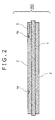
- Fig. 2 is a schematic view illustrating a cross section along line A-A' in Fig. 1
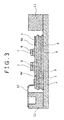
- Fig. 3 is a schematic cross sectional view of the semiconductor device of this embodiment.
- a circuit substrate 100 comprises an insulating substrate 1, and metal circuit layers 2 and 3 of a desired circuit pattern.
- the insulating substrate 1 comprises, for example, silicon nitride (Si 3 N 4 ), aluminum nitride (AlN), and alumina (Al 2 O 3 ).
- the metal circuit layers 2 and 3 each comprise, for example, a copper thin film, a copper thin film plated with nickel (Ni), and an aluminum (Al) thin film plated with nickel (Ni).
- a 2-dimensional bar code 5 is provided over the surface of the metal circuit layer 2.
- the 2-dimensional bar code 5 is marked on the surface of the metal circuit layer 2 by laser irradiation.
- the laser used for marking comprises, for example, a YV04 laser but other lasers than that described above may also be used.
- Solder flow prevention areas 4a and 4b are present in a region of metal bonding a metal terminal 10 on the surface of a metal circuit layer 2 by ultrasonic waves, that is, between an ultrasonic metal bonding region 53 as a metal wiring connection portion and a chip arranging region 51 and between a 2-dimensional bar code 5 and a chip arranging region 52.
- the solder flow prevention areas 4a and 4b are formed linearly in the metal circuit layer 2 and comprise a finely surface-roughened metal oxide.
- the surface of the solder flow prevention area is roughened compared with the surface of the metal circuit layer 2, and the thickness of the oxide on the surface of the solder flow prevention area is larger than that on the surface of the metal circuit layer 2.
- the metal oxide comprises, for example, copper oxide or, an oxide of a plating material, for example, a nickel oxide film when the metal circuit layer 2 is plated. A metal oxide less sensitive to reduction is more preferred.
- the solder flow prevention areas 4a and 4b are formed by laser irradiation to the surface of the metal circuit layer 2.
- the type of laser includes, for example, the YV04 laser but other type of lasers may also be used.
- the finely roughened surface can be formed by using, for example, pulse laser.
- a semiconductor device of a low cost and at high productivity can be obtained by forming the solder flow prevention area and marking the 2-dimensional bar code by an identical laser irradiation device.
- the width of the solder flow prevention area is preferably 0.01 mm or more and 0.1 mm or less, but the width may also be out of the range. It may suffice that the depth is less than the thickness of the metal circuit layer 2.
- a circuit substrate 100 in which a semiconductor chip 7 is connected by means of a solder 6 is mounted by the solder 8 to a metal base 9.
- a casing 11 is connected to the metal base 9 and a metal terminal 10 is connected by means of ultrasonic metal bonding to a predetermined position of the circuit substrate 100 by ultrasonic metal bonding (ultrasonic metal bonding region 53 in Fig. 1 ).
- the semiconductor chip 7 an IGBT chip or a diode chip is applicable.
- Wettability of solder to a copper oxide or nickel oxide is less than that to copper or nickel. Further, since a larger surface area is available in a finely uneven surface than in a planar surface, the surface tension of solder can be increased. In this embodiment illustrated in Fig. 1 , since the solder flow prevention areas 4a and 4b comprise copper oxide or nickel oxide in the finely roughened state, molten solder can be prevented from spreading.
- the solder flow prevention area may be provided optionally to a desired place. In this embodiment, the solder preventing area is provided between the ultrasonic metal bonding region 53 and the chip arranging region 51 and between the 2-dimensional bar code 5 and the chip arranging region 52.
- solder flow prevention area may be disposed, for example, also between the wire bonding connection region and the chip arranging region.
- the 2-dimensional bar code 5 is formed over the circuit substrate 100 by using a laser device for forming the solder flow prevention area. For example, identification number of an individual circuit substrate is registered in the 2-dimensional bar code. This can administrate the assembling data of parts such as chips mounted on the circuit substrate. Further, since the solder flow prevention area and the 2-dimensional bar code can be formed by using an identical laser irradiation device, cost for introducing the device can be saved.
- the solder flow prevention areas 4a and 4b described in this embodiment are provided each by one row between the chip arranging region 51 and the metal bonding region 53 or the 2-dimensional bar code 5, but they may be arranged each in a plurality of rows. Even if a great amount of molten solder spreads under wetting, solder that overrides the first row can be prevented from spreading by the second and succeeding rows by using a plurality rows of solder flow prevention areas.
- the size of the width and the pitch of the solder flow prevention area when they are arranged in a plurality rows is preferably 0.01 mm or more and 0.1 mm or less of width and 0.01 mm or more and 0.1 mm or less of pitch, but the width and the pitch may be out of the range described above.
- the 2-dimensional bar code is marked to the circuit substrate, but other marks than the 2-dimensional bar code, for example, other symbols, letters, etc. may also be marked.
- the semiconductor device of this embodiment is intended for preventing solder below the semiconductor chip from flowing
- this invention is also applicable to prevention of solder from flowing in connection of other electronic parts than the semiconductor chip, for example, a thermister which is connected by soldering.
- Fig. 4 is a schematic plan view illustrating a circuit substrate of a semiconductor device according to this embodiment
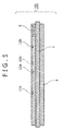
- Fig. 5 is a schematic view illustrating a cross section along line B-B' in Fig. 4
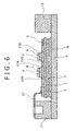
- Fig. 6 is a schematic cross sectional view of the semiconductor device according to this embodiment.
- solder flow prevention areas 12a and 12b surround chip arrangement regions 51 and 52.
- the following function and effect can be obtained in addition to the function and effect shown in the first embodiment.
- solder flow prevention areas 12a and 12b surround the chip arranging regions 51 and 52 respectively, but a plurality of chip arranging regions may be surrounded also by one solder flow prevention area. Since this can shorten the time of laser irradiation, productivity can be improved.
- the solver flow prevention area is not restricted to one row but may comprise a plurality of rows.
Landscapes
- Die Bonding (AREA)
- Chemical & Material Sciences (AREA)
- Engineering & Computer Science (AREA)
- Ceramic Engineering (AREA)
- Cooling Or The Like Of Semiconductors Or Solid State Devices (AREA)
Abstract
Description
- The present invention relates to a semiconductor device and particularly relates to a semiconductor device suitable to power application uses such as for motor control and a method of manufacturing the same.
- Power semiconductor devices are semiconductor devices used for controlling electric equipment such as motors. With an increasing demand for energy saving and reduction in environmental loads in recent years, inverter control for motors has been developed and a demand for the power semiconductor devices has been increased rapidly along with development of markets for hybrid cars and electric cars.
- In the power semiconductor device, a semiconductor chip for power control typically represented by IGBT (Insulated Gate Bipolar Transistor) or a rectifying diode chip is bonded by soldering over a metal circuit layer of a circuit substrate in which the metal circuit layer is formed over an insulating substrate. Then, a metal terminal such as made of copper (Cu) is bonded by means of ultrasonic metal bonding or a fine wire such as formed of aluminum (Al) or copper is bonded by wire bonding on one identical surface of the metal circuit layer where the chip and the solder are provided and connected directly or indirectly with a terminal of a casing of the power semiconductor device.
- In the step of assembling such a power semiconductor device, if the processing temperature is excessively high, it causes a problem that not only the solder below the chip is melted and spreads from the inside to the outside of the chip failing to ensure sufficient thickness of the solder below the chip but also ultrasonic metal bonding or wire bonding can no more be attained if the solder spreads as far as the ultrasonic metal bonding portion or a wire bonding portion of the metal terminal.
- The existent art for preventing the solder from flowing includes, for example, techniques disclosed in Japanese Unexamined Patent Application Publications Nos.
2004-71888 Hei 08(1996)-31848 2004-71888 Hei08(1996)-31848 - However, in the technique described in Japanese Unexamined Patent Application Publication No.
2004-71888 - Further, by the method described in Japanese Unexamined Patent Application Publication No.
Hei 08(1996)-31848 - The present invention has been achieved in view of the problems described above and it intends to provide a semiconductor device capable of effectively preventing solder below the chip from flowing at a reduced cost and with good productivity.
- In the semiconductor device according to an aspect of the invention, a solder flow prevention area comprising an oxide material finely roughened at the surface is provided between a chip arranging region and an ultrasonic metal bonding region or a wire bonding region of a circuit substrate by laser irradiation.
- Further, in the method of manufacturing a semiconductor device according to another aspect of the invention, a solder flow prevention area is formed by laser irradiation.
- According to the aspects of the invention, since solder flow can be prevented, even when the chip and the ultrasonic metal bonding portion or the wire bonding portion are situated at a short distance due to high integration degree, a semiconductor device of high reliability with no occurrence of assembling failure can be obtained.
-
-
Fig. 1 is a schematic plan view of a circuit substrate of a semiconductor device according to a first embodiment; -
Fig. 2 is a schematic cross sectional view of the circuit substrate of the semiconductor device according to the first embodiment; -
Fig. 3 is a schematic cross sectional view of the semiconductor device according to the first embodiment; -
Fig. 4 is a schematic plan view of a circuit substrate of a semiconductor device according to a second embodiment; -
Fig. 5 is a schematic cross sectional view of the circuit substrate of the semiconductor device according to the second embodiment; and -
Fig. 6 is a schematic cross sectional view of the semiconductor device according to the second embodiment. - Preferred embodiments of the present invention are to be described with reference to the drawings.
- A first embodiment of the invention is to be described with reference to
Fig. 1 to Fig. 3 . -
Fig. 1 is a schematic plan view illustrating a circuit substrate of a semiconductor device according to this embodiment,Fig. 2 is a schematic view illustrating a cross section along line A-A' inFig. 1 , andFig. 3 is a schematic cross sectional view of the semiconductor device of this embodiment. - A
circuit substrate 100 comprises aninsulating substrate 1, andmetal circuit layers insulating substrate 1 comprises, for example, silicon nitride (Si3N4), aluminum nitride (AlN), and alumina (Al2O3). Further, themetal circuit layers - A 2-
dimensional bar code 5 is provided over the surface of themetal circuit layer 2. The 2-dimensional bar code 5 is marked on the surface of themetal circuit layer 2 by laser irradiation. The laser used for marking comprises, for example, a YV04 laser but other lasers than that described above may also be used. - By the way, in the manufacture of semiconductor devices, hysteresis of inspection data for individual parts, etc. are administrated for product control. In the semiconductor devices in which parts are mounted on a casing, various conditions such as temperature in the assembling step and inspection data can be put to one-to-one correspondence to products by bonding a seal that describes product number to the case. In the same manner, while one-to-one correspondence is required in the step before mounting to the casing, that is, between individual parts and inspection data and assembling conditions also for the parts in which a chip, etc. are mounted over a circuit substrate as in this embodiment. According to the bar code used in this embodiment, hysteresis of assembling parts can be administrated even for parts in which the semiconductor chip, etc. are mounted over the circuit substrate.
- Solder
flow prevention areas metal terminal 10 on the surface of ametal circuit layer 2 by ultrasonic waves, that is, between an ultrasonicmetal bonding region 53 as a metal wiring connection portion and achip arranging region 51 and between a 2-dimensional bar code 5 and achip arranging region 52. The solderflow prevention areas metal circuit layer 2 and comprise a finely surface-roughened metal oxide. The surface of the solder flow prevention area is roughened compared with the surface of themetal circuit layer 2, and the thickness of the oxide on the surface of the solder flow prevention area is larger than that on the surface of themetal circuit layer 2. - The metal oxide comprises, for example, copper oxide or, an oxide of a plating material, for example, a nickel oxide film when the
metal circuit layer 2 is plated. A metal oxide less sensitive to reduction is more preferred. The solderflow prevention areas metal circuit layer 2. The type of laser includes, for example, the YV04 laser but other type of lasers may also be used. The finely roughened surface can be formed by using, for example, pulse laser. A semiconductor device of a low cost and at high productivity can be obtained by forming the solder flow prevention area and marking the 2-dimensional bar code by an identical laser irradiation device. - The width of the solder flow prevention area is preferably 0.01 mm or more and 0.1 mm or less, but the width may also be out of the range. It may suffice that the depth is less than the thickness of the
metal circuit layer 2. - In the schematic cross sectional view illustrated in
Fig. 3 , acircuit substrate 100 in which asemiconductor chip 7 is connected by means of asolder 6 is mounted by thesolder 8 to ametal base 9. Acasing 11 is connected to themetal base 9 and ametal terminal 10 is connected by means of ultrasonic metal bonding to a predetermined position of thecircuit substrate 100 by ultrasonic metal bonding (ultrasonicmetal bonding region 53 inFig. 1 ). As thesemiconductor chip 7, an IGBT chip or a diode chip is applicable. - The function and the effect of this embodiment are to be described below.
- Wettability of solder to a copper oxide or nickel oxide is less than that to copper or nickel. Further, since a larger surface area is available in a finely uneven surface than in a planar surface, the surface tension of solder can be increased. In this embodiment illustrated in
Fig. 1 , since the solderflow prevention areas metal bonding region 53 and thechip arranging region 51 and between the 2-dimensional bar code 5 and thechip arranging region 52. This can prevent the molten solder from spreading under wetting to the ultrasonicmetal bonding region 51 and the 2-dimensional bar code 5. In addition to the configuration of this embodiment, the solder flow prevention area may be disposed, for example, also between the wire bonding connection region and the chip arranging region. - Further, according to the semiconductor device of this embodiment, the 2-
dimensional bar code 5 is formed over thecircuit substrate 100 by using a laser device for forming the solder flow prevention area. For example, identification number of an individual circuit substrate is registered in the 2-dimensional bar code. This can administrate the assembling data of parts such as chips mounted on the circuit substrate. Further, since the solder flow prevention area and the 2-dimensional bar code can be formed by using an identical laser irradiation device, cost for introducing the device can be saved. - The solder
flow prevention areas chip arranging region 51 and themetal bonding region 53 or the 2-dimensional bar code 5, but they may be arranged each in a plurality of rows. Even if a great amount of molten solder spreads under wetting, solder that overrides the first row can be prevented from spreading by the second and succeeding rows by using a plurality rows of solder flow prevention areas. The size of the width and the pitch of the solder flow prevention area when they are arranged in a plurality rows is preferably 0.01 mm or more and 0.1 mm or less of width and 0.01 mm or more and 0.1 mm or less of pitch, but the width and the pitch may be out of the range described above. - In the semiconductor device of this embodiment, the 2-dimensional bar code is marked to the circuit substrate, but other marks than the 2-dimensional bar code, for example, other symbols, letters, etc. may also be marked.
- While the semiconductor device of this embodiment is intended for preventing solder below the semiconductor chip from flowing, this invention is also applicable to prevention of solder from flowing in connection of other electronic parts than the semiconductor chip, for example, a thermister which is connected by soldering.
- Then, a second embodiment of the invention is to be described with reference to
Fig. 4 to Fig. 6 . -
Fig. 4 is a schematic plan view illustrating a circuit substrate of a semiconductor device according to this embodiment, andFig. 5 is a schematic view illustrating a cross section along line B-B' inFig. 4 .Fig. 6 is a schematic cross sectional view of the semiconductor device according to this embodiment. - This embodiment is different from the first embodiment in that solder
flow prevention areas chip arrangement regions - According to the semiconductor device of this embodiment, the following function and effect can be obtained in addition to the function and effect shown in the first embodiment.
- According to the semiconductor device of this embodiment, since spreading of solder under wetting can be reduced more than that of the first embodiment, decrease in the film thickness of solder below the chip can be prevented. This can prevent, development of fatigue crackings generated in solder below the chip.
- In this embodiment, the solder
flow prevention areas chip arranging regions - In the same manner as in the first embodiment, the solver flow prevention area is not restricted to one row but may comprise a plurality of rows.
Claims (9)
- A semiconductor device in which a metal circuit layer (2) is provided over a main planar surface of an insulating substrate (1), a semiconductor chip (7) is connected by way of solder (6) over the metal circuit layer (2), and a metal wiring (10) is connected over the metal circuit layer,
wherein a linear oxide material is formed between the semiconductor chip (7) and the metal wiring connection portion over the surface of the metal circuit layer. - The semiconductor device according to claim 1, wherein the thickness of the oxide material is larger than the thickness of an oxide film over the metal circuit layer.
- The semiconductor device according to claim 1 or 2, wherein the surface of the oxide material is roughened more than the surface of the metal circuit layer.
- The semiconductor device according to any one of claims 1 to 3, wherein the oxide material is disposed so as to surround the semiconductor chip (7).
- The semiconductor device according to any one of claims 1 to 4, wherein a mark (5) is formed to the metal circuit layer (2).
- A method of manufacturing a semiconductor device in which a metal circuit layer (2) is provided over the main planar surface of an insulating substrate (1), a semiconductor chip (7) is connected by way of a solder (6) over the metal circuit layer (2), and a metal wiring (10) is connected over the metal circuit layer, the method comprising:forming a linear oxide material between the semiconductor chip (7) andthe metal wiring connection portion over the metal circuit layer.
- The method of manufacturing a semiconductor device according to claim 6, wherein the oxide material is formed by laser irradiation.
- The method of manufacturing a semiconductor device according to claim 6 or claim 7, wherein a mark (5) is formed over the metal circuit layer (2).
- The method of manufacturing a semiconductor device according to claim 8, wherein the mark is formed by laser irradiation.
Applications Claiming Priority (1)
| Application Number | Priority Date | Filing Date | Title |
|---|---|---|---|
| JP2012120376A JP2013247256A (en) | 2012-05-28 | 2012-05-28 | Semiconductor device and method of manufacturing the same |
Publications (2)
| Publication Number | Publication Date |
|---|---|
| EP2669938A2 true EP2669938A2 (en) | 2013-12-04 |
| EP2669938A3 EP2669938A3 (en) | 2014-04-09 |
Family
ID=48626263
Family Applications (1)
| Application Number | Title | Priority Date | Filing Date |
|---|---|---|---|
| EP13169401.0A Withdrawn EP2669938A3 (en) | 2012-05-28 | 2013-05-27 | Semiconductor device with an oxide solder flow prevention area on a substrate and corresponding manufacturing method |
Country Status (3)
| Country | Link |
|---|---|
| US (1) | US9076774B2 (en) |
| EP (1) | EP2669938A3 (en) |
| JP (1) | JP2013247256A (en) |
Cited By (3)
| Publication number | Priority date | Publication date | Assignee | Title |
|---|---|---|---|---|
| WO2014198511A1 (en) * | 2013-06-14 | 2014-12-18 | Robert Bosch Gmbh | Substrate having a soldering resist region consisting of oxide, sulfide or nitride for delimiting a soldering region and corresponding production process |
| EP3361504A1 (en) * | 2017-02-14 | 2018-08-15 | Infineon Technologies AG | Power electronic substrate with marker, manufacturing of a power electronic substrate and detection of a marker |
| US11587879B2 (en) | 2020-01-23 | 2023-02-21 | Fuji Electric Co., Ltd. | Electronic apparatus and manufacturing method thereof |
Families Citing this family (11)
| Publication number | Priority date | Publication date | Assignee | Title |
|---|---|---|---|---|
| WO2016092791A1 (en) * | 2014-12-10 | 2016-06-16 | 株式会社デンソー | Semiconductor device and method for manufacturing same |
| JP6578900B2 (en) * | 2014-12-10 | 2019-09-25 | 株式会社デンソー | Semiconductor device and manufacturing method thereof |
| EP3217428B1 (en) * | 2016-03-07 | 2022-09-07 | Infineon Technologies AG | Multiple substrate and method for the production of same |
| JP2017159335A (en) * | 2016-03-10 | 2017-09-14 | 株式会社デンソー | Semiconductor device and manufacturing method thereof |
| JP6485398B2 (en) * | 2016-04-13 | 2019-03-20 | 株式会社デンソー | Electronic device and manufacturing method thereof |
| JP7192241B2 (en) | 2018-05-01 | 2022-12-20 | 富士電機株式会社 | Semiconductor module and method for manufacturing semiconductor module |
| WO2021049039A1 (en) * | 2019-09-13 | 2021-03-18 | 株式会社デンソー | Semiconductor device |
| JP2021118350A (en) * | 2020-01-23 | 2021-08-10 | 富士電機株式会社 | Electronic device and manufacturing method for electronic device |
| JP7587570B2 (en) * | 2020-03-26 | 2024-11-20 | デンカ株式会社 | Ceramic circuit board, heat dissipation member, and aluminum-diamond composite |
| WO2023008200A1 (en) * | 2021-07-26 | 2023-02-02 | デンカ株式会社 | Bonded substrate, circuit board and manufacturing method therefor, and individual substrate and manufacturing method therefor |
| CN121215520A (en) * | 2024-04-25 | 2025-12-26 | 派德芯能半导体(上海)有限公司 | Solder mask packaging methods and solder mask packaging structures |
Citations (3)
| Publication number | Priority date | Publication date | Assignee | Title |
|---|---|---|---|---|
| JPH0831848A (en) | 1994-07-19 | 1996-02-02 | Fuji Electric Co Ltd | Method for manufacturing semiconductor device |
| US6063689A (en) * | 1998-07-06 | 2000-05-16 | United Microelectronics Corp. | Method for forming an isolation |
| JP2004071888A (en) | 2002-08-07 | 2004-03-04 | Mitsubishi Electric Corp | Circuit board for semiconductor device and semiconductor device |
Family Cites Families (9)
| Publication number | Priority date | Publication date | Assignee | Title |
|---|---|---|---|---|
| US6707152B1 (en) * | 1999-04-16 | 2004-03-16 | Micron Technology, Inc. | Semiconductor device, electrical conductor system, and method of making |
| JP2000332376A (en) | 1999-05-25 | 2000-11-30 | Mitsubishi Electric Corp | Semiconductor device marking method |
| DE10351120A1 (en) | 2003-11-03 | 2005-06-09 | eupec Europäische Gesellschaft für Leistungshalbleiter mbH | Lötstopbarriere |
| JP5102497B2 (en) * | 2007-01-19 | 2012-12-19 | Dowaメタルテック株式会社 | Method for manufacturing metal-ceramic bonded circuit board |
| JP5145729B2 (en) | 2007-02-26 | 2013-02-20 | 富士電機株式会社 | Solder bonding method and semiconductor device manufacturing method using the same |
| US20080237353A1 (en) | 2007-03-29 | 2008-10-02 | Joy Lau | Unique identifier on integrated circuit device |
| JP2009218280A (en) * | 2008-03-07 | 2009-09-24 | Toshiba Corp | Semiconductor device |
| JP5299303B2 (en) | 2010-02-05 | 2013-09-25 | 三菱マテリアル株式会社 | Power module substrate with identification symbol and method for manufacturing the same |
| CN102549738B (en) * | 2010-05-18 | 2015-07-01 | 丰田自动车株式会社 | Semiconductor device and method for manufacturing the same |
-
2012
- 2012-05-28 JP JP2012120376A patent/JP2013247256A/en active Pending
-
2013
- 2013-05-15 US US13/894,756 patent/US9076774B2/en active Active
- 2013-05-27 EP EP13169401.0A patent/EP2669938A3/en not_active Withdrawn
Patent Citations (3)
| Publication number | Priority date | Publication date | Assignee | Title |
|---|---|---|---|---|
| JPH0831848A (en) | 1994-07-19 | 1996-02-02 | Fuji Electric Co Ltd | Method for manufacturing semiconductor device |
| US6063689A (en) * | 1998-07-06 | 2000-05-16 | United Microelectronics Corp. | Method for forming an isolation |
| JP2004071888A (en) | 2002-08-07 | 2004-03-04 | Mitsubishi Electric Corp | Circuit board for semiconductor device and semiconductor device |
Non-Patent Citations (1)
| Title |
|---|
| ANUFRIENKO V F ET AL: "A Study of Linear Copper Oxide Structures in the Channels of the ZSM-5 Zeolite by Electronic Diffuse Reflectance Spectroscopy", DOKLADY PHYSICAL CHEMISTRY, vol. 392, no. 1-3, 2003, pages 207 - 211, XP055241273 * |
Cited By (3)
| Publication number | Priority date | Publication date | Assignee | Title |
|---|---|---|---|---|
| WO2014198511A1 (en) * | 2013-06-14 | 2014-12-18 | Robert Bosch Gmbh | Substrate having a soldering resist region consisting of oxide, sulfide or nitride for delimiting a soldering region and corresponding production process |
| EP3361504A1 (en) * | 2017-02-14 | 2018-08-15 | Infineon Technologies AG | Power electronic substrate with marker, manufacturing of a power electronic substrate and detection of a marker |
| US11587879B2 (en) | 2020-01-23 | 2023-02-21 | Fuji Electric Co., Ltd. | Electronic apparatus and manufacturing method thereof |
Also Published As
| Publication number | Publication date |
|---|---|
| EP2669938A3 (en) | 2014-04-09 |
| JP2013247256A (en) | 2013-12-09 |
| US20130313711A1 (en) | 2013-11-28 |
| US9076774B2 (en) | 2015-07-07 |
Similar Documents
| Publication | Publication Date | Title |
|---|---|---|
| US9076774B2 (en) | Semiconductor device and a method of manufacturing same | |
| US9691673B2 (en) | Power module semiconductor device | |
| US9391006B2 (en) | Semiconductor device and method of manufacturing semiconductor device | |
| EP2557633B1 (en) | Press fit terminal and semiconductor module | |
| US10529656B2 (en) | Semiconductor device | |
| US9159715B2 (en) | Miniaturized semiconductor device | |
| US9978664B2 (en) | Semiconductor module | |
| US20170133308A1 (en) | Semiconductor device and production method thereof | |
| US9142479B2 (en) | Electronic device and semiconductor device | |
| US9214418B2 (en) | Lead frame with radiator plate, method for manufacturing lead frame with radiator plate, semiconductor device, and method for manufacturing semiconductor device | |
| US10727150B2 (en) | Semiconductor module and power converter | |
| JP5262408B2 (en) | Positioning jig and method for manufacturing semiconductor device | |
| JP5795282B2 (en) | Electronic equipment | |
| US10141249B2 (en) | Molded intelligent power module and method of making the same | |
| US20170170150A1 (en) | Semiconductor module and semiconductor device | |
| CN105529277B (en) | Method for welding circuit carrier and carrier board | |
| US20240332141A1 (en) | Semiconductor device package for press fit assembly | |
| US20140078687A1 (en) | Device mounting board, semiconductor module, and method for fabricating the device mounting board | |
| US11195778B2 (en) | Electronic power module | |
| JP2005051109A (en) | Power semiconductor module | |
| JP2016001644A (en) | Semiconductor module | |
| US20260068737A1 (en) | Semiconductor module and manufacturing method of semiconductor module | |
| US12519041B2 (en) | Semiconductor module for a power semiconductor device | |
| JP2003318315A (en) | Transistor bare chip mounting wiring board and method of manufacturing the same | |
| CN107045991A (en) | Circuit module and its manufacture method |
Legal Events
| Date | Code | Title | Description |
|---|---|---|---|
| PUAI | Public reference made under article 153(3) epc to a published international application that has entered the european phase |
Free format text: ORIGINAL CODE: 0009012 |
|
| AK | Designated contracting states |
Kind code of ref document: A2 Designated state(s): AL AT BE BG CH CY CZ DE DK EE ES FI FR GB GR HR HU IE IS IT LI LT LU LV MC MK MT NL NO PL PT RO RS SE SI SK SM TR |
|
| AX | Request for extension of the european patent |
Extension state: BA ME |
|
| 17P | Request for examination filed |
Effective date: 20131016 |
|
| RBV | Designated contracting states (corrected) |
Designated state(s): AL AT BE BG CH CY CZ DE DK EE ES FI FR GB GR HR HU IE IS IT LI LT LU LV MC MK MT NL NO PL PT RO RS SE SI SK SM TR |
|
| PUAL | Search report despatched |
Free format text: ORIGINAL CODE: 0009013 |
|
| AK | Designated contracting states |
Kind code of ref document: A3 Designated state(s): AL AT BE BG CH CY CZ DE DK EE ES FI FR GB GR HR HU IE IS IT LI LT LU LV MC MK MT NL NO PL PT RO RS SE SI SK SM TR |
|
| AX | Request for extension of the european patent |
Extension state: BA ME |
|
| RIC1 | Information provided on ipc code assigned before grant |
Ipc: H01L 23/373 20060101ALI20140304BHEP Ipc: H01L 21/48 20060101ALI20140304BHEP Ipc: H01L 25/07 20060101ALN20140304BHEP Ipc: H01L 21/60 20060101AFI20140304BHEP Ipc: H01L 23/544 20060101ALI20140304BHEP |
|
| RAP1 | Party data changed (applicant data changed or rights of an application transferred) |
Owner name: HITACHI POWER SEMICONDUCTOR DEVICE, LTD. |
|
| 17Q | First examination report despatched |
Effective date: 20160120 |
|
| STAA | Information on the status of an ep patent application or granted ep patent |
Free format text: STATUS: THE APPLICATION IS DEEMED TO BE WITHDRAWN |
|
| 18D | Application deemed to be withdrawn |
Effective date: 20160531 |