EP2669912A1 - Power-feeding module of contactless power-feeding apparatus, method of using power-feeding module of contactless power-feeding apparatus, and method of manufacturing power-feeding module of contactless power-feeding apparatus - Google Patents
Power-feeding module of contactless power-feeding apparatus, method of using power-feeding module of contactless power-feeding apparatus, and method of manufacturing power-feeding module of contactless power-feeding apparatus Download PDFInfo
- Publication number
- EP2669912A1 EP2669912A1 EP12739194.4A EP12739194A EP2669912A1 EP 2669912 A1 EP2669912 A1 EP 2669912A1 EP 12739194 A EP12739194 A EP 12739194A EP 2669912 A1 EP2669912 A1 EP 2669912A1
- Authority
- EP
- European Patent Office
- Prior art keywords
- coil
- power supplying
- unit
- printed wiring
- wiring substrate
- Prior art date
- Legal status (The legal status is an assumption and is not a legal conclusion. Google has not performed a legal analysis and makes no representation as to the accuracy of the status listed.)
- Granted
Links
- 238000004519 manufacturing process Methods 0.000 title claims abstract description 41
- 238000000034 method Methods 0.000 title claims description 25
- 239000000758 substrate Substances 0.000 claims description 223
- 230000005540 biological transmission Effects 0.000 claims description 56
- 239000002184 metal Substances 0.000 claims description 42
- 238000001514 detection method Methods 0.000 claims description 40
- 229920005989 resin Polymers 0.000 claims description 14
- 239000011347 resin Substances 0.000 claims description 14
- 239000012212 insulator Substances 0.000 claims description 11
- 230000008878 coupling Effects 0.000 claims description 10
- 238000010168 coupling process Methods 0.000 claims description 10
- 238000005859 coupling reaction Methods 0.000 claims description 10
- 239000003990 capacitor Substances 0.000 claims description 9
- 230000005674 electromagnetic induction Effects 0.000 claims description 5
- 238000005304 joining Methods 0.000 abstract description 10
- 230000005284 excitation Effects 0.000 description 41
- 238000010586 diagram Methods 0.000 description 17
- 230000004907 flux Effects 0.000 description 12
- WABPQHHGFIMREM-UHFFFAOYSA-N lead(0) Chemical compound [Pb] WABPQHHGFIMREM-UHFFFAOYSA-N 0.000 description 10
- 239000000463 material Substances 0.000 description 7
- 238000012546 transfer Methods 0.000 description 6
- 238000013461 design Methods 0.000 description 5
- 230000007274 generation of a signal involved in cell-cell signaling Effects 0.000 description 4
- 238000009499 grossing Methods 0.000 description 4
- 230000004308 accommodation Effects 0.000 description 3
- 239000000284 extract Substances 0.000 description 3
- 229920003002 synthetic resin Polymers 0.000 description 3
- 239000000057 synthetic resin Substances 0.000 description 3
- 230000015572 biosynthetic process Effects 0.000 description 2
- 230000008859 change Effects 0.000 description 2
- 230000007423 decrease Effects 0.000 description 2
- 239000000696 magnetic material Substances 0.000 description 2
- 238000000465 moulding Methods 0.000 description 2
- 238000003825 pressing Methods 0.000 description 2
- 238000004804 winding Methods 0.000 description 2
- 238000004891 communication Methods 0.000 description 1
- RKTYLMNFRDHKIL-UHFFFAOYSA-N copper;5,10,15,20-tetraphenylporphyrin-22,24-diide Chemical compound [Cu+2].C1=CC(C(=C2C=CC([N-]2)=C(C=2C=CC=CC=2)C=2C=CC(N=2)=C(C=2C=CC=CC=2)C2=CC=C3[N-]2)C=2C=CC=CC=2)=NC1=C3C1=CC=CC=C1 RKTYLMNFRDHKIL-UHFFFAOYSA-N 0.000 description 1
- 230000035699 permeability Effects 0.000 description 1
- 239000011295 pitch Substances 0.000 description 1
- 238000012545 processing Methods 0.000 description 1
- 239000004065 semiconductor Substances 0.000 description 1
- 229910000859 α-Fe Inorganic materials 0.000 description 1
Images


Classifications
-
- H04B5/79—
-
- H—ELECTRICITY
- H01—ELECTRIC ELEMENTS
- H01F—MAGNETS; INDUCTANCES; TRANSFORMERS; SELECTION OF MATERIALS FOR THEIR MAGNETIC PROPERTIES
- H01F38/00—Adaptations of transformers or inductances for specific applications or functions
- H01F38/14—Inductive couplings
-
- H—ELECTRICITY
- H02—GENERATION; CONVERSION OR DISTRIBUTION OF ELECTRIC POWER
- H02J—CIRCUIT ARRANGEMENTS OR SYSTEMS FOR SUPPLYING OR DISTRIBUTING ELECTRIC POWER; SYSTEMS FOR STORING ELECTRIC ENERGY
- H02J50/00—Circuit arrangements or systems for wireless supply or distribution of electric power
- H02J50/10—Circuit arrangements or systems for wireless supply or distribution of electric power using inductive coupling
- H02J50/12—Circuit arrangements or systems for wireless supply or distribution of electric power using inductive coupling of the resonant type
-
- H—ELECTRICITY
- H02—GENERATION; CONVERSION OR DISTRIBUTION OF ELECTRIC POWER
- H02J—CIRCUIT ARRANGEMENTS OR SYSTEMS FOR SUPPLYING OR DISTRIBUTING ELECTRIC POWER; SYSTEMS FOR STORING ELECTRIC ENERGY
- H02J50/00—Circuit arrangements or systems for wireless supply or distribution of electric power
- H02J50/40—Circuit arrangements or systems for wireless supply or distribution of electric power using two or more transmitting or receiving devices
- H02J50/402—Circuit arrangements or systems for wireless supply or distribution of electric power using two or more transmitting or receiving devices the two or more transmitting or the two or more receiving devices being integrated in the same unit, e.g. power mats with several coils or antennas with several sub-antennas
-
- H—ELECTRICITY
- H02—GENERATION; CONVERSION OR DISTRIBUTION OF ELECTRIC POWER
- H02J—CIRCUIT ARRANGEMENTS OR SYSTEMS FOR SUPPLYING OR DISTRIBUTING ELECTRIC POWER; SYSTEMS FOR STORING ELECTRIC ENERGY
- H02J50/00—Circuit arrangements or systems for wireless supply or distribution of electric power
- H02J50/60—Circuit arrangements or systems for wireless supply or distribution of electric power responsive to the presence of foreign objects, e.g. detection of living beings
-
- H—ELECTRICITY
- H02—GENERATION; CONVERSION OR DISTRIBUTION OF ELECTRIC POWER
- H02J—CIRCUIT ARRANGEMENTS OR SYSTEMS FOR SUPPLYING OR DISTRIBUTING ELECTRIC POWER; SYSTEMS FOR STORING ELECTRIC ENERGY
- H02J50/00—Circuit arrangements or systems for wireless supply or distribution of electric power
- H02J50/80—Circuit arrangements or systems for wireless supply or distribution of electric power involving the exchange of data, concerning supply or distribution of electric power, between transmitting devices and receiving devices
-
- H—ELECTRICITY
- H02—GENERATION; CONVERSION OR DISTRIBUTION OF ELECTRIC POWER
- H02J—CIRCUIT ARRANGEMENTS OR SYSTEMS FOR SUPPLYING OR DISTRIBUTING ELECTRIC POWER; SYSTEMS FOR STORING ELECTRIC ENERGY
- H02J50/00—Circuit arrangements or systems for wireless supply or distribution of electric power
- H02J50/90—Circuit arrangements or systems for wireless supply or distribution of electric power involving detection or optimisation of position, e.g. alignment
-
- H—ELECTRICITY
- H05—ELECTRIC TECHNIQUES NOT OTHERWISE PROVIDED FOR
- H05K—PRINTED CIRCUITS; CASINGS OR CONSTRUCTIONAL DETAILS OF ELECTRIC APPARATUS; MANUFACTURE OF ASSEMBLAGES OF ELECTRICAL COMPONENTS
- H05K13/00—Apparatus or processes specially adapted for manufacturing or adjusting assemblages of electric components
- H05K13/04—Mounting of components, e.g. of leadless components
-
- H—ELECTRICITY
- H02—GENERATION; CONVERSION OR DISTRIBUTION OF ELECTRIC POWER
- H02J—CIRCUIT ARRANGEMENTS OR SYSTEMS FOR SUPPLYING OR DISTRIBUTING ELECTRIC POWER; SYSTEMS FOR STORING ELECTRIC ENERGY
- H02J50/00—Circuit arrangements or systems for wireless supply or distribution of electric power
- H02J50/70—Circuit arrangements or systems for wireless supply or distribution of electric power involving the reduction of electric, magnetic or electromagnetic leakage fields
-
- Y—GENERAL TAGGING OF NEW TECHNOLOGICAL DEVELOPMENTS; GENERAL TAGGING OF CROSS-SECTIONAL TECHNOLOGIES SPANNING OVER SEVERAL SECTIONS OF THE IPC; TECHNICAL SUBJECTS COVERED BY FORMER USPC CROSS-REFERENCE ART COLLECTIONS [XRACs] AND DIGESTS
- Y10—TECHNICAL SUBJECTS COVERED BY FORMER USPC
- Y10T—TECHNICAL SUBJECTS COVERED BY FORMER US CLASSIFICATION
- Y10T29/00—Metal working
- Y10T29/49—Method of mechanical manufacture
- Y10T29/49002—Electrical device making
- Y10T29/4902—Electromagnet, transformer or inductor
Abstract
Description
- The present invention relates to a power supplying module for a contactless power supplying device, a method for using the power supplying module of the contactless power supplying device, and a method for manufacturing the power supplying module of the contactless power supplying device.
- In recent years, various types of practical systems that use a contactless power supplying technique have been proposed. For example, a large number of power supplying modules, each having a plurality of power supplying coils, are laid along a transfer route. A moving body including a power receiving coil is arranged on the transfer route. The moving body generates secondary power at the power receiving coil through electromagnetic induction resulting from excitation of the power supplying coils in the power supplying modules laid along the transfer route. The secondary power is used to drive, for example, a motor and thus move the moving body (patent document 1).
- Patent Document 1: Japanese Laid-Open Patent Publication No.
2006-121791 - In the contactless power supplying system, each of the large number of power supplying modules laid along the transfer route is configured by integrally forming a single power supplying coil and a power supplying circuit that controls excitation of that power supplying coil. The power supplying circuit includes a central processing unit (CPU) and a read-only semiconductor memory (ROM) just for the single power supplying coil. The power supplying circuit is thus a complex and expensive power supplying module. Furthermore, each power supplying module has a complex structure since a commercial power supply is input to each power supplying module. Therefore, each power supplying module is very expensive.
-
Patent document 1 discloses a method for laying out the power supplying modules along the transfer route. The task of assembling the complex power supplying modules on the transfer route is very cumbersome and requires effort and time. - Therefore, there is a limitation to the freedom of design for an area where the power supplying modules can be laid out and supplied with power.
- It is an object of the present invention to provide a power supplying module for a contactless power supplying device, a method for using the power supplying module of the contactless power supplying device, and a method for manufacturing the power supplying module of the contactless power supplying device that has a high degree of freedom for design, allows for contactless power supply in various modes, and enables manufacturing that is easy and performed within a short period of time.
- A power supplying module for a contactless power supplying device according to the present invention includes a plurality of coil units. Each of the coil units includes a primary coil and one or more first terminals. When the primary coil is excited and a secondary coil of a device is arranged adjacent to the primary coil, secondary power is generated by electromagnetic induction at the secondary coil, and the secondary power is supplied to a load of the device. A printed wiring substrate includes a plurality of first layout regions respectively defined for arrangement of the coil units. Each of the first layout regions includes one or more second terminals for connection to the one or more first terminals of the corresponding coil unit. One or more wires are formed on the printed wiring substrate to drive the coil unit arranged in each of the first layout regions. The coil units are arranged on the printed wiring substrate by arranging the coil units in the first layout regions of the printed wiring substrate and connecting the one or more second terminals of each first layout region to the one or more first terminals of each coil unit.
- In the above configuration, the first layout regions are defined to set a linear power suppliable region in which the coil units are arranged on the printed wiring substrate in a single line in either one of a front-back direction and a left-right direction.
- In the above configuration, the first layout regions are defined to set a planar power suppliable region in which the coil units are arranged in front-back and left-right directions on the printed wiring substrate is set.
- In the above configuration, the coil units arranged in the front-back and left-right directions on the printed wiring substrate satisfy "A" < "F" and "B" < "F", where "A" represents the distance between two coil units adjacent in the left-right direction, "B" represents the distance between two coil units adjacent in the front-back direction, and "F" represents the longest distance among a side and a diameter or a diagonal line of the secondary coil of a device, which includes the secondary coil having the smallest coil area, among devices usable for the power supplying module.
- In the above configuration, the plurality of first layout regions are defined to set a circular or a sector-shaped power suppliable region so that the coil units are arranged at different angles relative to the printed wiring substrate.
- In the above configuration, the coil units have the same specification.
- In the above configuration, each of the coil units includes a coil portion having the primary coil, a drive portion with an inverter circuit that excites the primary coil, and an insulating resin that integrally molds the coil portion and the drive portion.
- In the above configuration, each of the coil units includes a reception unit that receives a signal from the device.
- In the above configuration, each of the coil units includes at least one of a device authentication unit, a metal detection unit, and a data transmission/reception unit, which transmits and receives data to and from the device.
- In the above configuration, the primary coils of each of the coil units are wound around a core formed by a magnetic body.
- The above configuration includes a resonance capacitor connected to the primary coil of each of the coil units.
- In the above configuration, the primary coil of each of the coil units has a cuboid shape.
- The above configuration includes an insulator arranged on the coil units arranged on the printed wiring substrate. Power suppliable to the device is set by changing a thickness of the insulator.
- In the above configuration, each of the first layout regions formed on the printed wiring substrate is a coil unit fitting recess into which the coil unit is fitted. Each of the coil unit fitting recesses includes a bottom surface, and the one or more second terminals formed on the bottom surface of each of the coil unit fitting recesses and connected to the one or more first terminals of the coil unit that is fitted.
- The above configuration includes a system unit that centrally drives and controls each of the coil units and includes a plurality of third terminals, and a second layout region defined and formed on the printed wiring substrate for arrangement of the system unit. The second layout region includes a plurality of fourth terminals respectively connected to the third terminals of the system unit, and the third terminals of the system unit and the one or more first terminals of each coil unit are electrically connected.
- The above configuration includes a power suppliable region section that is defined on the printed wiring substrate and is applicable to a device of a further standardized specification. A plurality of coil units for the device of the further standardized specification are arranged in the power suppliable region section.
- The above configuration includes a magnetic member that electromagnetically shields the coil unit in the coil units arranged on the printed wiring substrate.
- The above configuration includes planarly arranging a plurality of identical power supplying modules in conformance with a power suppliable region.
- The above configuration includes three-dimensionally arranging a plurality of identical power supplying modules in conformance with a power suppliable region.
- A method for manufacturing a power supplying module of a contactless power supplying device according to the present invention includes preparing a printed wiring substrate and a plurality of coil units. Each of the coil units includes a primary coil and one or more first terminals. When the primary coil is excited and the secondary coil of the device is arranged adjacent to the primary coil, secondary power is generated by electromagnetic induction at the secondary coil, and the secondary power is supplied to a load of the device. The printed wiring substrate includes a plurality of first layout regions respectively defined for arrangement of the coil units, one or more second terminals formed in each of the first layout regions for connection to the one or more first terminals of the corresponding coil unit, and one or more wires formed on the printed wiring substrate to drive the coil unit arranged in each of the first layout regions. The method further includes arranging the coil units in at least one of the first layout regions of the printed wiring substrate, connecting the one or more second terminals of the first layout region in which the coil units are arranged and the one or more first terminals of the corresponding coil unit, and coupling the plurality of coil units to the printed wiring substrate.
- In the above configuration, the arranging includes arranging the coil units in all of the first layout regions formed in the printed wiring substrate, and respectively coupling the coil units to all of the first layout regions of the printed wiring substrate.
- In the above configuration, the arranging includes selecting one or more of the first layout regions formed in the printed wiring substrate in accordance with a preset power suppliable region, arranging the coil unit in the selected first layout region on the printed wiring substrate, and coupling the coil units to the selected first layout region on the printed wiring substrate.
- In the above configuration, the coil units have the same specification.
- In the above configuration, the first layout regions formed on the printed wiring substrate are coil unit fitting recesses to which the coil units are fitted. Each of the coil unit fitting recesses includes a bottom surface, and the one or more second terminals formed on the bottom surface of each of the coil unit fitting recesses and connected to the one or more first terminals of the coil unit that is fitted.
- In the above configuration, the one or more second terminals formed in each of the first layout regions on the printed wiring substrate are flip-chip connected to the one or more first terminals formed in each of the coil units.
- In the above configuration, the one or more second terminals formed in each of the first layout regions on the printed wiring substrate are connected by a male-type contact plug terminal and a female-type contact plug terminal to the one or more terminals formed in each of the coil units.
- The present invention provides a power supplying module for a contactless power supplying device having a high degree of freedom for design, allowing for contactless power supply in various modes, and enabling manufacturing that is easy and performed within a short period of time.
-
Fig. 1 is an overall perspective view of a contactless power supplying device of a first embodiment. -
Fig. 2 is an overall perspective view of a power supplying module. -
Fig. 3 is an exploded perspective view of the power supplying module. -
Fig. 4 is a cross-sectional view of a coil unit. -
Fig. 5 is an overall perspective view of a coil portion of the coil unit. -
Fig. 6 is a cross-sectional view of a system unit. -
Fig. 7 is schematic diagram showing the layout of the coil units on a printed wiring substrate. -
Fig. 8 is an electric circuit diagram showing an electrical configuration of the contactless power supplying device. -
Fig. 9 is an exploded perspective view of a power supplying module showing another example of the first embodiment.. -
Fig. 10 is an overall perspective view of the power supplying module. -
Fig. 11 is an overall perspective view of the power supplying module. -
Fig. 12 is an overall perspective view of the power supplying module. -
Fig. 13 is an overall perspective view of the power supplying module. -
Fig. 14 is an overall perspective view of the power supplying module. -
Fig. 15 is an overall perspective view of the power supplying module. -
Fig. 16 is an overall perspective view of the power supplying module. -
Fig. 17 is an overall perspective view of the power supplying module. -
Fig. 18 is an overall perspective view of the power supplying module. -
Fig. 19 is an overall perspective view of the power supplying module. -
Fig. 20 is an overall perspective view of the power supplying module. -
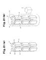
Fig. 21(a) is a diagram showing the arrangement of a plurality of power supplying modules, andFig. 21(b) is a diagram showing the plurality of power supplying modules arranged in a column. -
Fig. 22(a) is a diagram showing the arrangement of the plurality of power supplying modules, andFig. 22(b) is a diagram showing the plurality of power supplying modules arranged in a box. -
Fig. 23 is a view in which the power supplying module is arranged under a floor. -
Fig. 24 is an exploded perspective view of a power supplying module of a second embodiment. -
Fig. 25 is an overall perspective view of the power supplying module. -
Fig. 26(a) is a diagram showing a connecting state of the coil unit and the drive unit,Fig. 26(b) is a diagram showing a connecting state of the drive unit for coil units connected in series, andFig. 26(c) is a diagram showing a connecting state of the drive unit for coil units connected in parallel. -
Fig. 27 is a diagram showing another example of the second embodiment in which a resonance capacitor is connected to the primary coil and the secondary coil. -
Fig. 28 is an overall perspective view of a power supplying module capable of performing supplying power to a device of another standardized specification. -
Fig. 29 is an electric circuit diagram showing an electrical configuration of the power supplying device. -
Fig. 30 is schematic diagram showing another method for forming the coil unit fitting recess and the system unit fitting recess. -
Fig. 31 is a diagram showing another arrangement method of the coil unit. -
Fig. 32(a) is a diagram showing a positional relationship with the secondary coil when the coil units are arranged in a lattice form, andFig. 32(b) is a diagram showing a positional relationship with the secondary coil of when the coil units are arranged in a zigzagged manner. -
Fig. 33 is a diagram showing the system unit separated from the printed wiring substrate. -
Fig. 34 is a side view showing a state in which the coil units and the system unit are arranged on a mold frame. - A first embodiment of a contactless power supplying device according to a contactless power supplying system of the present invention will now be described with reference to the drawings.
- As shown in
Fig. 1 , a contactlesspower supplying device 1 includes ahousing 2. Thehousing 2 includes atetragonal box body 3, which has an upper opening, and atop plate 4, which is formed by an insulating body and closes the opening of thebox body 3. Thetop plate 4 includes asetting surface 5, which is an upper surface of the contactlesspower supplying device 1 for mounting a device E to supply power in a contactless manner. - As shown in
Fig. 2 , a power supplying module M is accommodated in thehousing 2. The power supplying module M includes a printedwiring substrate 10, a plurality of coil units CU, and a system unit SU. The plurality of coil units CU are arranged on the printedwiring substrate 10 and electrically connected to the printedwiring substrate 10. The system unit SU is arranged on the printedwiring substrate 10 and electrically connected to the printedwiring substrate 10. The system unit SU centrally controls the coil units CU. - In the present embodiment, the printed
wiring substrate 10 is a multi-layered printed wiring substrate. As shown inFig. 3 , the printedwiring substrate 10 includes anupper surface 10a. Theupper surface 10a includes a total of 18 coil unit fitting recesses 11, three in a front-back direction and six in a left-right direction. In the present embodiment, each coilunit fitting recess 11 is a rectangular recess having a long side that extends in the front-back direction. An interval between adjacent coil unit fitting recesses 11 in the left-right direction is fixed. The coil unit CU is fitted into the coilunit fitting recess 11. The coil unit CU includes electrodes P having a plurality of external input/output terminals (seeFig. 4 ). - A system
unit fitting recess 12 is formed on a left back side of theupper surface 10a of the printedwiring substrate 10. In the present embodiment, the length in the front-back direction of the systemunit fitting recess 12 is the same as the length in the front-back direction of the coilunit fitting recess 11. The length in the left-right direction of the systemunit fitting recess 12 is longer than the length in the left-right direction of the coilunit fitting recess 11. The system unit SU for drive controlling each coil unit CU is fitted into the systemunit fitting recess 12. The system unit SU includes electrodes P having a plurality of external input/output terminals (seeFig. 6 ). - Each coil
unit fitting recess 11 includes a bottom surface S1. Each bottom surface S1 includes a plurality of pads PD, each of which is electrically connected to the electrodes P of the plurality of external input/output terminals of the coil unit CU (seeFig. 4 ). - Each bottom surface S2 of the system
unit fitting recess 12 of the printedwiring substrate 10 includes a plurality of pads PD, each of which is electrically connected to the electrodes P of the plurality of external input/output terminals of the system unit SU (seeFig. 6 ). - The printed
wiring substrate 10 includes a plurality of wires IN for electrically connecting each coil unit CU and the system unit SU. As shown inFig. 2 , each coil unit CU and the system unit SU are electrically connected through the plurality of wires IN by fitting the system unit SU to the systemunit fitting recess 12 and fitting the coil unit CU to each coilunit fitting recess 11. - The material, shape, and size of each coil unit CU have the same specification. As shown in
Fig. 3 , each coil unit CU is a rectangular parallelepiped so that each coil unit CU can be fitted into the coilunit fitting recess 11. Each coil unit CU has outer side surfaces including a lower surface. As shown inFig. 4 , the outer side surface excluding the lower surface of each coil unit CU is molded from an insulatingresin 13. As shown inFig. 4 andFig. 5 , each coil unit CU is formed by integrating acoil portion 14a and adrive portion 14b, which is configured by resin molding a circuit substrate having circuit elements of various types of circuits such as an inverter circuit for excitation driving a primary coil L1 to the lower surface of thecoil portion 14a. Eachcoil portion 14a includes a rectangular parallelepiped-shaped core C, which has a large magnetic permeability such as ferrite core, the primary coil L1 wound around the core C, and the lower surface. Eachdrive portion 14b includes the circuit substrate, which includes circuit elements of various types of circuits such as the inverter circuit for excitation driving the primary coil L1, and a lower surface. Each circuit substrate is resin molded to the lower surface of thecoil portion 14a. In other words, each coil unit CU of the present embodiment is an inverter integrated coil unit. - Each
coil portion 14a includes a signal reception antenna AT1 and a metal detection antenna AT2. Each signal reception antenna AT1 is arranged to surround the primary coil L1 on an outer side of the upper end of the primary coil L1 in thecoil portion 14a and fixed to the primary coil L1. Each metal detection antenna AT2 is arranged to surround the core C at an inner side of the upper end of the primary coil L1, and is fixed to the primary coil L1. - As shown in
Fig. 4 , the electrodes P having the plurality of external input/output terminals are formed on the lower surface of eachdrive portion 14b (surface on the bottom surface S1 side of the coil unit fitting recess 11). The electrodes P having the plurality of external input/output terminals are respectively electrically connected to the plurality of pads PD on the printedwiring substrate 10. Therefore, in each coil unit CU molded from the insulatingresin 13, only the plurality of electrodes P are formed in a projecting manner from the lower surface of each coil unit CU. - As shown in
Fig. 2 , when the inverter integrated coil unit CU fitted into each coilunit fitting recess 11 is electrically connected to the wire IN formed on the printedwiring substrate 10, the upper surface of the coil unit CU projects from theupper surface 10a of the printedwiring substrate 10. - The plurality of electrodes P of each coil unit CU and the plurality of pads PD formed on the bottom surface S1 of each coil
unit fitting recess 11 are joined by applying pressure and ultrasonic waves to the coil unit CU (e.g., flip-chip) toward the bottom surface of the coilunit fitting recess 11. - A power suppliable region AR is a region that surrounds a total of 18 coil units, three in the front-back direction and six in the left-right direction, arranged on the printed
wiring substrate 10 at the upward position of the printedwiring substrate 10. That is, when changing the power suppliable region AR, the power suppliable region AR can be easily changed by simply changing the layout of the plurality of coil units CU arranged on the printedwiring substrate 10. - A large number of coil unit fitting recesses 11 of the printed
wiring substrate 10 may be formed in advance, the predetermined plurality of coil unit fitting recesses 11 may be selected from the large number of coil unit fitting recesses 11 in accordance with the desired power suppliable region AR of the user, and the plurality of coil units CU may be fitted into the plurality of selected coil unit fitting recesses 11. In this case, various power suppliable regions AR requested by the user can be easily selected by simply selecting the coilunit fitting recess 11 as requested by the user, and fitting the coil unit CU to the plurality of selected coil unit fitting recesses 11. - The arrangement interval of the coil units CU can also be easily set. The supplying power requested by the user can be selected by simply changing the arrangement interval of the coil units CU.
- As shown in
Fig. 3 , the system unit SU is a rectangular parallelepiped so that the system unit SU can be fitted into the systemunit fitting recess 12. As shown inFig. 6 , the outer side surface excluding the lower surface of the system unit SU is molded from an insulatingresin 15. The system unit SU includes a system control unit 36 (seeFig. 8 ) including a microcomputer that centrally controls thedrive portion 14b of each coil unit CU. The system unit SU also includes acircuit substrate 18, on which adevice 17 is configured by resin molding a power supply circuit and the like. Thecircuit substrate 18 requests for drive power to each coil unit CU. Thecircuit substrate 18 is molded from the insulatingresin 15. - The system unit SU (circuit substrate 18) includes a lower surface (surface on the bottom surface S2 side of the system unit fitting recess 12) provided with the electrodes P of the plurality of external input/output terminals, each of which is electrically connected to the plurality of pads PD on the printed
wiring substrate 10 formed in correspondence with the system unit SU. Therefore, in the system unit SU molded from the insulatingresin 15, only the plurality of electrodes P are formed projecting from the lower surface of the system unit SU. As shown inFig. 2 , when the system unit SU fitted into the systemunit fitting recess 12 is electrically connected to the printedwiring substrate 10, the upper surface of the system unit SU projects from theupper surface 10a of the printedwiring substrate 10. - Each electrode P of the system unit SU and each pad PD formed on the bottom surface S2 of the system
unit fitting recess 12 are joined by applying pressure and ultrasonic waves to the system unit SU (e.g., flip-chip) toward the bottom surface of the systemunit fitting recess 12 in the same manner as described above. - Each coil unit CU is driven based on a control of the system unit SU. That is, the primary coil L1 of each coil unit CU is excited alone or is excited in cooperation with another primary coil L1.
- The plurality of (18 in the present embodiment) coil units CU can thus be easily coupled to the printed
wiring substrate 10 by simply fitting the coil unit CU into each coilunit fitting recess 11 formed in the printedwiring substrate 10 and joining each coilunit fitting recess 11 with the coil unit CU. This improves the manufacturing efficiency of the contactlesspower supplying device 1. Furthermore, since each coil unit CU has the same specification and can be mass-produced, the coil unit CU can be formed with low costs. Moreover, the number of components and the manufacturing steps of the coil unit CU are fewer, and the component management is also easier compared to when coupling coil units of different specifications. - The system unit SU can be easily coupled to the printed
wiring substrate 10 by simply fitting the system unit SU into the systemunit fitting recess 12 formed in the printedwiring substrate 10 and joining the systemunit fitting recess 12 with the system unit SU. Furthermore, the system unit SU is electrically connected to each coil unit CU by the plurality of wires IN of the printedwiring substrate 10. Thus, the wiring step of the system unit SU and each coil unit CU is very simple, and the manufacturing efficiency of the contactlesspower supplying device 1 can be improved. - The power supplying module M including the printed
wiring substrate 10, to which the system unit SU and the plurality of coil units CU are assembled, is accommodated in thebox body 3 of thehousing 2. Thebox body 3 of thehousing 2 is closed with thetop plate 4. When thebox body 3 is closed with thetop plate 4, the upper surface of each coil unit CU is arranged at a position proximate to the lower surface of thetop plate 4, and the device E is set on thesetting surface 5 of thetop plate 4. - As shown in
Fig. 1 , the device E set on thesetting surface 5 of the contactlesspower supplying device 1 includes a secondary coil L2. The secondary coil L2 of the device E is excited and supplied with power through the excitation of the primary coil L1 of the contactlesspower supplying device 1, and supplies the supplied secondary power to a load Z (seeFig. 8 ) of the device E. - As shown in
Fig. 1 , a transmission/reception antenna AT3 is arranged to surround the secondary coil L2 at an outer side of the secondary coil L2 of the device E. When set on thesetting surface 5 of the contactlesspower supplying device 1, the device E exchanges data and information through wireless communication with thedrive portion 14b of the coil unit CU through the signal reception antenna AT1 surrounding the primary coil L1 of the coil unit CU located immediately below the device E. - A metal detection antenna AT4 is arranged at an inner side of each secondary coil L2. The metal detection antenna AT4 detects a metal piece arranged between the setting
surface 5 and the device E when the device E is set on thesetting surface 5. - The relative position of the plurality of coil units CU, that is, the formation position (first layout region) of each coil
unit fitting recess 11 is set based on the one of the devices E, which may be used for the power supplying module M, including the secondary coil L2 having the smallest coil area. - In detail, if the plurality of coil units CU are arranged in the front-back and left-right directions, that is, in the planar direction, as shown in
Fig. 7 , the distance between two coil units CU adjacent in the left-right direction is represented by "A", and the distance between two coil units CU adjacent in the front-back direction is represented by "B". - The one of the devices that can be used for the contactless power supplying device 1 (power supplying module M) including the secondary coil L2 having the smallest coil area is selected. The one among the side and the diameter or the diagonal line of the selected device E with the secondary coil L2 having the smallest coil area is set as distance "F".
- Each coil unit CU is arranged on the printed
wiring substrate 10 so as to satisfy the relationships "A"<"F" and "B"<"F". - If such conditions are satisfied, wherever the secondary coil L2 of the device E is arranged on the power suppliable region AR, at least a portion of the primary coil L1 overlaps with the secondary coil L2 of the device E immediately below the secondary coil L2. By avoiding a situation in which there are no primary coils L1 immediately below the secondary coil L2 of the subject device E, a large decrease in the magnetic flux density of the power supplying surface is prevented. The secondary coil L2 may generate a minimum induced electromotive force regardless of where the secondary coil L2 is arranged on the power suppliable region AR. This obtains the minimum voltage required and the required output for the device E.
- The electrical configuration of the contactless power supplying device 1 (power supplying module M) and the device will now be described with reference to
Fig. 8 . - As shown in
Fig. 8 , the device E includes a rectifying/smoothingcircuit 21, a voltage/current control circuit 22, an authenticationsignal generation circuit 23, a device transmission/reception circuit 24, an inverteradjustment control circuit 25, ametal detection circuit 26, and a load Z. The secondary coil L2 of the device E is excited and supplied with power through the excitation of the primary coil L1 of the power supplying module M (coil unit CU), and outputs the supplied secondary power to the rectifying/smoothingcircuit 21. The rectifying/smoothingcircuit 21 converts the secondary power to a DC (Direct Current) voltage without ripples, and outputs the DC voltage to the voltage/current control circuit 22. The voltage/current control circuit 22 voltage/current controls the DC voltage, and supplies the DC voltage to the load Z of the device E. - The authentication
signal generation circuit 23 generates a device authentication signal ID for the contactlesspower supplying device 1 indicating that the device E is the one that is to receive power from the contactlesspower supplying device 1. The device authentication signal ID generated by the authenticationsignal generation circuit 23 is output to the device transmission/reception circuit 24. The device transmission/reception circuit 24 is connected to the transmission/reception antenna AT3, and transmits the device authentication signal ID to the contactlesspower supplying device 1 through the transmission/reception antenna AT3. - The device transmission/
reception circuit 24 exchanges data with the load Z to acquire data on the present electrical state of the load Z. The device transmission/reception circuit 24 transmits the acquired data to the contactlesspower supplying device 1 through the transmission/reception antenna AT3. - Furthermore, the inverter
adjustment control circuit 25 is connected to the device transmission/reception circuit 24. The inverteradjustment control circuit 25 controls the excitation state of the primary coil L1 of the power supplying module M in accordance with the condition of the voltage/current control circuit 22. The inverteradjustment control circuit 25, for example, calculates the drive capacity of the voltage/current control circuit 22 for the load Z that continuously changes, and transmits the data of the drive capacity to the contactlesspower supplying device 1 through the transmission/reception antenna AT3. - The device transmission/
reception circuit 24 is connected to themetal detection circuit 26. Themetal detection circuit 26 is connected to the metal detection antenna AT4. The metal detection antenna AT4 detects a metal piece arranged between the settingsurface 5 and the device E. When the metal detection antenna AT4 detects a metal piece arranged between the settingsurface 5 and the device E, themetal detection circuit 26 transmits a metal-present signal ST to the device transmission/reception circuit 24. The device transmission/reception circuit 24 transmits the metal-present signal ST to the contactlesspower supplying device 1 through the transmission/reception antenna AT3. - As shown in
Fig. 8 , thedrive portion 14b arranged in each coil unit CU includes a deviceauthentication reception circuit 31, ametal detection circuit 32, a data transmission/reception circuit 33, anexcitation control circuit 34, and a highfrequency inverter circuit 35. - The device
authentication reception circuit 31 is connected to the signal reception antenna AT1 of thecoil portion 14a of the coil unit CU. When the device E is set on thesetting surface 5 immediately above the coil unit CU, the deviceauthentication reception circuit 31 receives the transmission signal transmitted from the device transmission/reception circuit 24 of the device E through the signal reception antenna AT1. The deviceauthentication reception circuit 31 extracts the device authentication signal ID indicating that the device E is the device E that can receive power supply from the received transmission signal. After extracting the device authentication signal ID from the transmission signal, the deviceauthentication reception circuit 31 outputs the device authentication signal ID to theexcitation control circuit 34. - The
metal detection circuit 32 is connected to the metal detection antenna AT2 arranged in thecoil portion 14a. Themetal detection circuit 32 detects whether or not a metal piece is set on thesetting surface 5 immediately above or proximate to the coil unit CU through the metal detection antenna AT2. When detecting that a metal piece is set on thesetting surface 5, themetal detection circuit 32 outputs the metal-present signal ST to theexcitation control circuit 34. - When the device E is set on the
setting surface 5 immediately above the coil unit CU, themetal detection circuit 32 receives the transmission signal transmitted from the device transmission/reception circuit 24 of the device E through the signal reception antenna AT1. Themetal detection circuit 32 extracts the metal-present signal ST from the received transmission signal. When extracting the metal-present signal ST from the transmission signal, themetal detection circuit 32 outputs the metal-present signal ST to theexcitation control circuit 34. - The data transmission/
reception circuit 33 is connected to the signal reception antenna AT1 of thecoil portion 14a. When the device E is set on thesetting surface 5 immediately above the coil unit CU, the data transmission/reception circuit 33 receives the transmission signal transmitted from the device transmission/reception circuit 24 of the device E through the signal reception antenna AT1. The data transmission/reception circuit 33 extracts various types of data from the device E from the received transmission signal. When extracting the various types of data from the transmission signal, the data transmission/reception circuit 33 outputs such data to theexcitation control circuit 34. - The device authentication signal ID from the device
authentication reception circuit 31 that is presently output, the metal-present signal ST from themetal detection circuit 32, and the various types of data from the data transmission/reception circuit 33 are input to theexcitation control circuit 34. Theexcitation control circuit 34 adds a position identification signal, which identifies its coil unit CU, to the device authentication signal ID that is presently input, the metal-present signal ST, and the various types of data. Theexcitation control circuit 34 outputs the device authentication signal ID, the metal-present signal ST, the various types of data, and the position identification signal to thesystem control unit 36 arranged in the system unit SU through the plurality of wires IN of the printedwiring substrate 10. - The
excitation control circuit 34 waits for a permission signal from thesystem control unit 36 when outputting the device authentication ID, the metal-present signal ST, and the various types of data. - The
system control unit 36 outputs to theexcitation control circuit 34 the permission signal for exciting and driving the primary coil L1 of the coil unit CU to supply power when the device authentication signal ID is input. Theexcitation control circuit 34 outputs a drive control signal CT for exciting and driving the primary coil L1 to supply power to the highfrequency inverter circuit 35 arranged in thedrive portion 14b when the permission signal from thesystem control unit 36 is input. - The
system control unit 36 does not output the permission signal even if the device authentication signal ID is input when the metal-present signal ST is input from theexcitation control circuit 34. Therefore, theexcitation control circuit 34 does not output the drive control signal CT for excitation driving the primary coil L1 to the highfrequency inverter circuit 35. - Furthermore, the
system control unit 36 stops the output of the permission signal when the device authentication signal ID from theexcitation control circuit 34 is no longer input while outputting the permission signal. Therefore, theexcitation control circuit 34 also does not output the drive control signal CT to the highfrequency inverter circuit 35 in this case. - The high
frequency inverter circuit 35 is connected to the primary coil L1 arranged in thecoil portion 14a of the coil unit CU. The highfrequency inverter circuit 35 oscillates at a predetermined frequency in accordance with the drive control signal CT to excite and drive the primary coil L1. - In detail, the high
frequency inverter circuit 35 excites and drives the primary coil L1 when the drive control signal CT for exciting and driving the primary coil L1 is input from theexcitation control circuit 34. - Therefore, when the device E that can receive power from the contactless power supplying device 1 (power supplying module M) is set on the
setting surface 5 immediately above the coil unit CU, the device authentication signal ID is transmitted from the device E, and a metal piece is not present in the vicinity of the device E, the primary coil L1 is excited and driven by the highfrequency inverter circuit 35. In other words, the primary coil L1 is excited and driven to supply the secondary power to the device E from the secondary coil L2 through contactless power supply. - The
system control unit 36 arranged in the system unit SU includes a microcomputer. Thesystem control unit 36 is electrically connected to thedrive portion 14b of each of the coil units CU through the wires IN formed on the printedwiring substrate 10. Thesystem control unit 36 inputs the device authentication ID, the metal-present signal ST, and the various types of data, which includes the position identification signal for identifying the coil unit CU, from theexcitation control circuit 34 of eachdrive portion 14b. - The
system control unit 36 determines whether or not the device E that can be supplied with power and is requesting for power supply is set immediately above thedrive portion 14b of the coil unit CU based on the device authentication signal ID from theexcitation control circuit 34 of thedrive portion 14b. - When the device authentication signal ID is input from the
excitation control circuit 34 of thedrive portion 14b, thesystem control unit 36 outputs the permission signal to theexcitation control circuit 34 of thedrive portion 14b. That is, thesystem control unit 36 determines that the device E that can be supplied with power and that is requesting for power supply is set immediately above thedrive portion 14b, and outputs the permission signal to theexcitation control circuit 34 of thedrive portion 14b. - If the size of the device E that can be supplied with power and is requesting for power supply is large and set on the
setting surface 5 of the contactlesspower supplying device 1, two or more coil units CU (coil portions 14a) may be positioned immediately underneath. - In this case, the
drive portion 14b of each coil unit CU (coil portion 14a) positioned immediately below the device E receives the device authentication signal ID of the device E. Eachdrive portion 14b then outputs the device authentication signal ID of the device E to thesystem control unit 36. - The
system control unit 36 determines whether or not the device E set immediately above each coil unit CU is the same as the device corresponding to the device authentication signal ID based on the device authentication signal ID including the position identification signal from thedrive portion 14b of each coil unit CU. - In this case, if the size of the device E is large, each coil unit CU can be determined from a group of coil units CU that are adjacent to each other and not separated using the position identification signal for identifying each coil unit CU and the device authentication signal ID.
- The
system control unit 36 then simultaneously outputs the permission signal to thedrive portions 14b (excitation control circuits 34) of the plurality of coil units CU, which is a group that is positioned immediately below the mounted device E having a large size and outputting the device authentication signal ID. - Therefore, the plurality of
drive portions 14b of the plurality of coil units CU cooperate to excite the plurality of primary coils L1 of the corresponding plurality of coil units CU, and supply power to the one device E having a large size. - Two or more devices E requesting for power supply may be set on the
setting surface 5 of the contactlesspower supplying device 1. - In this case, the
drive portion 14b corresponding to the coil unit CU (coil portion 14a) positioned immediately below each device E receives the device authentication signal ID for the corresponding device E and outputs the device authentication signal ID to thesystem control unit 36. - The
system control unit 36 determines whether or not the device E set immediately above each coil unit CU is not one but two or more based on the device authentication signal ID including the position identification signal from thedrive portion 14b of each coil unit CU. - In this case, if two or more devices E are mounted, it may be determined that the coil units CU are located at separate positions with the position identification signal and the device authentication signal ID from the
drive portion 14b of each coil unit CU. - The
system control unit 36 outputs the permission signal to thedrive portion 14b for each coil unit CU that is located immediately below the two or more set devices E and that output the device authentication signal ID. Therefore, thedrive portion 14b of the coil unit CU corresponding to each device E excites the primary coil L1 of thecoil portion 14a, and supplies power to each device E. - The
system control unit 36 determines that the metal piece is set immediately above each coil unit CU based on the metal-present signal ST from thedrive portion 14b (excitation control circuit 34) of each coil unit CU. When the metal-present signal ST is input from theexcitation control circuit 34 of thedrive portion 14b to thesystem control unit 36, thesystem control unit 36 does not output the permission signal to theexcitation control circuit 34 of thedrive portion 14b. That is, thesystem control unit 36 determines that the metal piece is set immediately above the coil unit CU, and does not output the permission signal to thedrive portion 14b (excitation control circuit 34) of the coil unit CU. - When various types of data including the position identification signal is input from the
drive portion 14b of each coil unit CU to thesystem control unit 36, thesystem control unit 36 determines the state of the load Z of the device E set immediately above the coil unit CU and the state of the voltage/current control circuit 22. Thesystem control unit 36 then calculates an amplitude value for exciting the primary coil L1 arranged in thecoil portion 14a of the coil unit CU at an optimum amplitude and a frequency value for exciting at an optimum frequency to optimize the state of the load Z of the device E and the state of the voltage/current control circuit 22. Thesystem control unit 36 then outputs the amplitude value and the frequency value to thecorresponding drive portion 14b (excitation control circuit 34). - The
excitation control circuit 34 outputs the amplitude value and the frequency value calculated by thesystem control unit 36 to the highfrequency inverter circuit 35. The highfrequency inverter circuit 35 oscillates based on the amplitude value and the frequency value, and excites and drives the primary coil L1. The device E set immediately above the coil unit CU thus receives the optimum secondary power, and can control the state of the load Z and the state of the voltage/current control circuit 22 to an optimum state. - The manufacturing method of the power supplying module M will now be described.
- With regard to the power supplying module M for the contactless
power supplying device 1, the size of the power suppliable region AR is set, and the number of coil units CU and the layout of the coil units CU are determined for the set size of the power suppliable region AR. After the number and the layout of coil units CU are determined, the printedwiring substrate 10 having a size that fits the layout is set. Then, with respect to the printedwiring substrate 10 of which the size has been determined, the coilunit fitting recess 11 is formed at a desired position for each coil unit CU, and the systemunit fitting recess 12 is formed at a desired position (second arrangement section) for the system unit SU. - The pad PD is formed on the bottom surface of each coil
unit fitting recess 11 in accordance with the electrode P of the coil unit CU, and the pad PD is formed on the bottom surface of the systemunit fitting recess 12 in accordance with the electrode P of the system unit SU. - With regard to the printed
wiring substrate 10, the plurality of wires IN for electrically connecting the system unit SU fitted into the systemunit fitting recess 12 and the coil unit CU fitted into each coilunit fitting recess 11 are designed and manufactured. - For such printed
wiring substrate 10 formed in advance, the flip-chip coil unit CU is fitted into each coilunit fitting recess 11, and the plurality of pads PD of the printedwiring substrate 10 and the plurality of electrodes P of the coil units CU are respectively joined. In the same manner, the flip-chip system unit SU is fitted into the systemunit fitting recess 12, and the plurality of pads PD of the printedwiring substrate 10 and the plurality of electrodes P of the system unit SU are respectively joined. - Thus, a plurality of (18 in the present embodiment) coil units CU are coupled to the printed
wiring substrate 10, and the system unit SU for centrally controlling each coil unit CU is coupled to the printedwiring substrate 10. This manufactures the power supplying module M. - The power supplying module M in which the system unit SU and the plurality of coil units CU are coupled to the printed
wiring substrate 10 is then accommodated in thebox body 3 of thehousing 2 and closed by thetop plate 4. This completes the contactlesspower supplying device 1. - First, the printed
wiring substrate 10, which includes the systemunit fitting recess 12 and the large number of coil unit fitting recesses 11, is formed in advance. In this case, the plurality of pads PD are formed on the bottom surface S2 of the systemunit fitting recess 12, and the plurality of pads PD are also formed on the bottom surface S1 of the large number of coil unit fitting recesses 11. Furthermore, the plurality of wires IN for electrically connecting the plurality of pads PD formed on the bottom surface S2 of the systemunit fitting recess 12 and the plurality of pads PD formed in the coil unit fitting recesses 11 are formed. - The coil
unit fitting recess 11 that is to be used is selected from the large number of coil unit fitting recesses 11 using the printedwiring substrate 10 including the systemunit fitting recess 12 and the large number of coil unit fitting recesses 11. That is, for example, the coil unit fitting recesses 11 positioned within the power suppliable region AR, which is set in accordance with the request of the user, are selected. - The flip-chip coil unit CU is fitted into each selected coil
unit fitting recess 11 within the desired power suppliable region AR of the user, and the plurality of pads PD of the printedwiring substrate 10 and the plurality of electrodes P of each coil unit CU are respectively joined. In the same manner, the flip-chip system unit SU is fitted into the systemunit fitting recess 12, and the plurality of pads PD of the printedwiring substrate 10 and the plurality of electrodes P of the system unit SU are respectively joined. - In the manufacturing method, the necessary coil
unit fitting recess 11 is selected in the printedwiring substrate 10 including the large number of coil unit fitting recesses 11. The coil unit CU is coupled to the selected coilunit fitting recess 11. The system unit SU for centrally controlling each coil unit CU is coupled to the printedwiring substrate 10. This manufactures the power supplying module M. - In this case, the large number of coil unit fitting recesses 11 are formed in advance in the printed
wiring substrate 10. The necessary coilunit fitting recess 11 is selected, and the coil unit CU is coupled to the selected coilunit fitting recess 11. Thus, the same printedwiring substrate 10 is applicable to various power suppliable regions AR. - The first embodiment has the advantages described below.
- (1) The first embodiment uses the plurality of coil units CU including the primary coils L1 of the same specification. The coil unit fitting recesses 11 are formed in the printed
wiring substrate 10 in conformance with the plurality of coil units CU. The plurality of pads PD, which are respectively joined with the plurality of electrodes P formed in the coil unit CU, are formed on the bottom surface S1 of each coilunit fitting recess 11. - Therefore, the plurality of coil units CU are easily coupled to the printed
wiring substrate 10 by simply fitting and joining each coil unit CU to the corresponding coilunit fitting recess 11. This improves the manufacturing efficiency. - In addition, each coil unit CU has the same specification with respect to material, shape, and size, and the coil units CU of the same specification are used. Thus, the coil unit CU may be mass-produced. This reduces costs of the coil unit CU.
- Moreover, since the coil units CU of the same specification are used, the number of components of the coil unit CU is small, and there are few manufacturing steps. This facilitates component management.
- (2) In the first embodiment, the primary coil L1 of each coil unit CU is configured to be wound around the core C, which is formed by a magnetic body. Therefore, the primary coil L1 is miniaturized as compared with an air core coil, and the size of the contactless power supplying device 1 (power supplying module M) is reduced. Furthermore, the miniature primary coil increases the power supplying capacity and improves the power supplying efficiency.
- (3) In the first embodiment, the system
unit fitting recess 12 is formed in the printedwiring substrate 10. The plurality of pads PD, which are to be joined with the plurality of electrodes P formed on the system unit SU, are formed on the bottom surface S2 of the systemunit fitting recess 12. The system unit SU for centrally controlling each coil unit CU is fitted into the systemunit fitting recess 12 to join the systemunit fitting recess 12 and the system unit SU. Therefore, the system unit SU is easily coupled to the printedwiring substrate 10. - Furthermore, the system unit SU is electrically connected to each coil unit CU through the plurality of wires IN of the printed
wiring substrate 10. Thus, the wiring step of the system unit SU and each coil unit CU is significantly simplified, and the manufacturing efficiency of the power supplying module M is improved. - (4) In the first embodiment, the plurality of coil unit fitting recesses 11 and the system
unit fitting recess 12 are formed in the printedwiring substrate 10. The plurality of coil units CU and the system unit SU are fitted into the plurality of coil unit fitting recesses 11 and the systemunit fitting recess 12. Therefore, the coupling task for arranging the coil unit CU and the system unit SU on the printedwiring substrate 10 is easily and accurately performed. - (5) In the first embodiment, the system unit SU and the plurality of coil units CU are coupled to the printed
wiring substrate 10 to manufacture one power supplying module M. The power supplying module M integrates the printedwiring substrate 10, the system unit SU, and the plurality of coil units CU. Thus, a large number of power suppliable power supplying modules M can be simultaneously transported. In addition, the step of accommodating in thebox body 3 of thehousing 2, which is performed at different location, merely includes accommodating only the power supplying module M in thebox body 3. Thus, the operation step of accommodating in thebox body 3 of thehousing 2 is very simple and completed within a short time. - (6) According to the first embodiment, the large number of coil unit fitting recesses 11 is formed in advance in the printed
wiring substrate 10. The necessary coilunit fitting recess 11 is selected in accordance with the power suppliable region AR, and the same coil unit CU is coupled to the selected coil unit fitting recesses 11 to form the power supplying module M. Therefore, the same printedwiring substrate 10 is applicable to various power suppliable regions AR, and the degree of freedom in design for the same printedwiring substrate 10 is increased. - Furthermore, since the plurality of the same coil units CU are coupled, a plurality of the same coil units CU are mass-produced. This lowers the price of the coil unit CU. Moreover, since a plurality of the same coil units CU are coupled, there are no complicated assembling tasks, and the efficiency is achieved.
- (7) In the first embodiment, one power suppliable power supplying module M is configured to couple the system unit SU and the plurality of coil units CU to the printed
wiring substrate 10. Thus, the mode of the power suppliable power supplying module M, that is, the shape of the printedwiring substrate 10, the number of coil units CU, and the arrangement state of the plurality of coil units CU are simply and easily changed in accordance with the power suppliable region AR. - Furthermore, in the present embodiment, each coil unit CU has a rectangular parallelepiped shape. The power supplying module M having a linear power suppliable region AR can be formed by arranging the plurality of coil units CU in the longitudinal directions along a single line. The power supplying module M having a wide and elongated power suppliable region may be formed by arranging the plurality of coil units CU in the short-side direction along a single line. Therefore, a power supplying module M having the linear power suppliable region AR and a power supplying module M having the wide elongated power suppliable region AR are realized using one type of coil unit CU.
- For example, as shown in
Fig. 9 and Fig. 10 , a plurality of coil unit fitting recesses 11, which extend in the front-back direction and into which the plurality of coil units CU are fitted, and the systemunit fitting recess 12, into which the system unit SU is fitted, are formed in the linear printedwiring substrate 10 extending in the front-back direction. The coil unit CU is fitted into each coilunit fitting recess 11 to join the plurality of coil unit fitting recesses 11 and the plurality of coil units CU. The system unit SU is fitted into the systemunit fitting recess 12 to join the systemunit fitting recess 12 and the system unit SU. This easily forms the power supplying module M having the linear power suppliable region AR extending in the front-back direction. - As shown in
Fig. 11 , a plurality of coil unit fitting recesses 11 and the systemunit fitting recess 12 are formed in the linear printedwiring substrate 10 extending in the left-right direction so that the plurality of coil units CU and the system unit SU, which longitudinal directions are directed in the left-right direction, are adjacent to each other. The plurality of coil units CU are fitted into the plurality of coil unit fitting recesses 11 formed in the linear printedwiring substrate 10 to join the plurality of coil unit fitting recesses 11 and the plurality of coil units CU. The system unit SU is fitted into the systemunit fitting recess 12 to join the systemunit fitting recess 12 and the system unit SU. This easily manufactures the power supplying module M having the linear power suppliable region AR extending in the left-right direction and in which two coil units CU are adjacent to each other. - As shown in
Fig. 12 , the plurality of coil units CU and the system unit SU are arranged together in the left-right direction on the linear printedwiring substrate 10 extending in the left-right direction so that the plurality of coil units CU and the system unit SU, of which the longitudinal directions are opposed in the front-back direction, are adjacent to each other. This allows for easy manufacturing of the power supplying module M including the linear power suppliable region AR arranged in the left-right direction so that the plurality of coil units CU and the system unit SU, of which the longitudinal directions are opposed in the front-back direction, are adjacent to each other. - Furthermore, as shown in
Fig. 13 , the plurality of coil units CU are arranged in parallel on the planar printedwiring substrate 10 extending in the front-back and left-right directions so that the plurality of coil units CU adjacent to each other in the front-back direction are also adjacent to each other in the left-right direction. This allows for easy manufacturing of the power supplying module M having the planar power suppliable region AR in which the plurality of coil units CU adjacent to each other in the front-back direction are adjacent to each other. - The first embodiment may be performed as described below.
- As shown in
Fig. 14 , amagnetic sheet 41 serving as the magnetic member made of magnetic material for electromagnetic shield may be arranged on the lower surface of the printedwiring substrate 10 of the power supplying module M. A magnetic body film may be formed between layers in the printedwiring substrate 10 of the multi-layered printed wiring substrate. - Thus, noise can be prevented without increasing the size of the power supplying module M (printed wiring substrate 10).
- As shown in
Fig. 15 , the power supplying module M having the linear power suppliable region AR shown inFig. 11 is arranged vertically. The power supplying module M may, for example, be arranged along awall 42 in this state. In the same manner, as shown inFig. 16 , the power supplying module M having the linear power suppliable region AR shown inFig. 11 is arranged horizontally. The power supplying module M may, for example, be arranged along thewall 42 in this horizontal state. - Furthermore, as shown in
Fig. 17 , a plurality of (two inFig. 17 ) power supplying modules M having the linear power suppliable region AR are arranged in parallel in the vertical direction. For example, the plurality of power supplying modules M may be arranged along thewall 42. In this case, the device E can receive power supply from the plurality of power supplying modules M, and thus can receive a large power. - In these cases, the power supplying modules M may be directly arranged on the
wall 42, or the power supplying modules M may be installed while being accommodated in thehousing 2. The power supplying modules M may be arranged on thewall 42. - As shown in
Fig. 18 , the plurality of (four inFig. 15 ) power suppliable power supplying modules M of the first embodiment may be adjacently arranged in the front-back and left-right directions. In this case, power can be supplied from the plurality of power supplying modules M to one device E. The device E thus can receive a large power. - As shown in
Fig. 19 , the power supplying module M in which the plurality of coil units CU are arranged on the printedwiring substrate 10 at equal angular intervals in the circumferential direction with the arrangement angle of the plurality of coil units CU changed may be formed. In this case, a circular power suppliable region AR can be formed. The power supplying module M including the spread power suppliable region AR can thus be provided. The power supplying module M in which the plurality of coil units CU are arranged in a fan-shape with respect to the printedwiring substrate 10 may be formed. In this case, the sector-shaped power suppliable region can be formed. The power supplying module M including the spread power suppliable region AR thus can be provided. For example, by arranging or embedding the sector-shaped or circular power supplying module M on or in a table, the power can be supplied by simply placing the device E at a place set as the power suppliable region of the table. - As shown in
Fig. 20 , the power supplying module M in which the plurality of coil units CU arranged at an equiangular interval in the circumferential direction are arranged in plurals with respect to the printedwiring substrate 10 of large size may be formed. In this case, a plurality of power suppliable regions AR can be formed. - As shown in
Figs. 21 (a), and 21 (b) (the drawings do not show the printed wiring substrate 10), the power supplying module M having the linear power suppliable region AR as shown inFig. 15 may be combined three-dimensionally in the vertical direction so that a plurality of (four in the figure) printedwiring substrates 10 face the inner side. For example, as shown inFig. 21 (b) , the three-dimensional contactless power supplying device including the plurality of power supplying modules M may be arranged or embedded on or in a circular column-shapedcolumn 44. This enables power supply at the surface of thecolumn 44. - As described above, the power supplying module M shown in
Fig. 12 is configured to arrange together the plurality of coil units CU and the system unit SU, of which longitudinal directions are opposed in the front-back direction, in the left-right direction to be adjacent to each other on the printedwiring substrate 10 extending in the left-right direction. As shown inFigs. 22(a) and 22(b) (the drawings do not show the printed wiring substrate 10), the power supplying module M may be three-dimensionally combined into a box-shape so that the plurality of (four in the drawing) printedwiring substrates 10 face the outer side. - The three-dimensional (box-shaped) contactless power supplying device including a plurality of power supplying modules M may, for example, be arranged on
plates 45a to 45e configuring anaccommodation box 45 or inside theplates 45a to 45e, as shown inFig. 22(b) . This enables power supply in theaccommodation box 45. - Each coil unit CU has the same specification, and the primary coil L1 of the
coil portion 14a of each coil unit CU also has the same specification. However, for example, only the number of windings of the primary coil L1 may be changed without changing the outer shape of each coil unit CU. - The interval between the coil units CU may be appropriately changed to change the average magnetic flux density in accordance with the power supplying capacity for supplying power.
- An insulator having a thickness may be arranged on the plurality of coil units CU arranged on the printed
wiring substrate 10. The suppliable power to the device E can be set by changing the thickness of the insulator. That is, the receiving power and the receiving voltage can be changed even in the contactless power supplying device having the same supplying power performance when the distance between the contactless power supplying device (power supplying module M) and the device E is changed by interposing the insulator. Thus, power can be supplied to various devices E. - Apparently, one insulator may be arranged on all of the upper surfaces of the plurality of coil units CU arranged on the printed
wiring substrate 10. - When the power supplying module M is used accommodated in the
housing 2, the thickness of thetop plate 4 may be changed. As shown inFig. 23 , when the contactless power supplying device (power supplying module M) is arranged under afloor plate 46, the suppliable power to the device E can be set by setting the interval between thefloor plate 46 and the contactless power supplying device 1 (power supplying module M). - In the first embodiment, the depth of the plurality of coil unit fitting recesses 11 and the system
unit fitting recess 12 is the depth at which the plurality of coil units CU and the system unit SU project from theupper surface 10a. However, the depth may be the depth at which the upper surfaces of the plurality of coil units CU and the system unit SU are flush with theupper surface 10a of the printedwiring substrate 10, or the emerging depth. - In the first embodiment, the plurality of coil unit fitting recesses 11 and the system
unit fitting recess 12 are formed, the coil unit CU is fitted into each coilunit fitting recess 11, and the system unit SU is fitted into the systemunit fitting recess 12. However, the coilunit fitting recess 11 and the systemunit fitting recess 12 may be omitted. - In the first embodiment, the system unit SU is coupled to the printed
wiring substrate 10 for the power supplying module M. However, the power supplying module M may be configured such that the system unit SU is omitted and the plurality of coil units CU are coupled to the printedwiring substrate 10. - In the first embodiment, the
drive portion 14b of the coil unit CU includes the deviceauthentication reception circuit 31, themetal detection circuit 32,the data transmission/reception circuit 33, theexcitation control circuit 34, and the highfrequency inverter circuit 35. There is no such limitation, and thedrive portion 14b of the coil unit CU may include the deviceauthentication reception circuit 31, themetal detection circuit 32, the data transmission/reception circuit 33, and theexcitation control circuit 34, excluding the highfrequency inverter circuit 35. Thedrive portion 14b of the coil unit CU may have all components omitted, or at least one omitted from the configuration of the first embodiment. If all are omitted, the detection of the device E is detected with another means, and thesystem control unit 36 drive controls the highfrequency inverter circuit 35 based on such detection. - A second embodiment of the present invention will now be described.
- The coil unit CU of the first embodiment is configured by the
coil portion 14a and thedrive portion 14b. In contrast, the coil unit of the second embodiment has thedrive portion 14b omitted from the coil unit CU of the first embodiment. - As shown in
Fig. 24 , eight coil unit fitting recesses 11 a are formed in the left-right direction at the back side of theupper surface 10a of the printedwiring substrate 10. Eight drive unit fitting recesses 11b and one systemunit fitting recess 12 are formed in the left-right direction on the front side of theupper surface 10a of the printedwiring substrate 10. - Each coil
unit fitting recess 11 a has a rectangular shape extending in the front-back direction. The coil unit fitting recesses 11 a are formed at equal pitches from the adjacent coil unitfitting recess 11a in the left-right direction. Each driveunit fitting recess 11b has a rectangular shape extending in the front-back direction, and is formed in juxtaposition with each coilunit fitting recess 11 a formed on the back side of theupper surface 10a. The systemunit fitting recess 12 is adjacently formed on the left side of the plurality of drive unit fitting recesses 11 b. - A coil unit CUa is fitted into each coil unit
fitting recess 11a. A drive unit CUb is fitted into each driveunit fitting recess 11 b. The system unit SU is fitted into the systemunit fitting recess 12. - Each coil unit CUa of the second embodiment includes the
coil portion 14a having a cuboid shape in which thedrive portion 14b of the coil unit CU shown in the first embodiment is omitted. That is, each coil unit CUa of the second embodiment includes thecoil portion 14a of the first embodiment shown inFig. 4 andFig. 5 , and is molded from the insulatingresin 13. On the lower surface of each coil unit CUa, the electrodes P of a plurality of external input/output terminals are electrically connected respectively with the drive unit CUb through the plurality of wires IN formed on the printedwiring substrate 10. - Each coil unit CUa is formed with the same specification in terms of material, shape, and size.
- Each drive unit CUb includes the
drive portion 14b in which thecoil portion 14a of the coil unit CU shown in the first embodiment is omitted. That is, the drive unit CUb of the second embodiment includes thecoil portion 14a of the first embodiment shown inFig. 4 , and is molded from the insulatingresin 13. On the lower surface of each drive unit CUb is formed the electrodes P of a plurality of external input/output terminals to be electrically connected respectively with the coil unit CUa and the system unit SU through the plurality of wires IN formed on the printedwiring substrate 10. - Each drive unit CUb is formed with the same specification in terms of material, shape, and size.
- Each drive unit CUb is electrically connected with the coil unit CUa. Each drive unit CUb excites and drives the primary coil L1 of the coil unit CUa. Furthermore, each drive unit CUb inputs the reception signal received by the signal reception antenna AT1 arranged in the coil unit CUa and the metal-present signal ST received by the metal detection antenna AT2.
- The system unit SU includes the
system control unit 36, which includes the microcomputer for centrally controlling each drive unit CUb, the power supply circuit, and the like, similar to the first embodiment. The lower surface of the system unit SU includes the electrodes P of a plurality of external input/output terminals electrically connected with the drive unit CUb through the plurality of wires IN formed on the printedwiring substrate 10, respectively. - A plurality of pads PD, each of which is electrically connected to the electrodes P of the plurality of external input/output terminals of the coil unit CUa fitted into the coil
unit fitting recess 11 a, are formed on a bottom surface S1a of each coil unitfitting recess 11a of the printedwiring substrate 10. A plurality of pads PD, each of which is electrically connected to the electrodes P of the plurality of external input/output terminals of the drive unit CUb fitted into the driveunit fitting recess 11 b, are formed on a bottom surface S1b of each driveunit fitting recess 11 b of the printedwiring substrate 10. - A plurality of pads PD, each of which is electrically connected to the electrodes P of the plurality of external input/output terminals of the system unit SU fitted into the system
unit fitting recess 12, are formed on a bottom surface S2 of the systemunit fitting recess 12 of the printedwiring substrate 10. - As shown in
Fig. 25 , the coil unit CUa is fitted into the coilunit fitting recess 11 a. The drive unit CUb is fitted into each driveunit fitting recess 11 b. This joins the corresponding electrode P and the pad PD. Therefore, the coil unit CUa and the drive unit CUb extending in the front-back direction are electrically connected through the plurality of wires IN formed on the printedwiring substrate 10. - The system unit SU is fitted into the system
unit fitting recess 12. The system unit SU and each drive unit CUb are electrically connected through the plurality of wires IN formed on the printedwiring substrate 10 by joining the electrode P and the pad PD. - The manufacturing method of the power supplying module M configured as above will now be described.
- With regard to the power supplying module M, the size of the power suppliable region AR is set. The number of coil units CUa, the number of drive units CUb, and the layout of the coil units CUa and the drive units CUb are determined for the set size of the power suppliable region AR. After the numbers and the layout of the coil units CUa and the drive units CUb are determined, the printed
wiring substrate 10 having a size that fits the layout is set. - Then, with respect to the printed
wiring substrate 10 in which the size is determined, the coilunit fitting recess 11 a and the driveunit fitting recess 11 b are formed at positions to arrange each coil unit CUa and each drive unit Cub as desired, and the systemunit fitting recess 12 is formed at a position to arrange the system unit SU as desired. - The plurality of pads PD are formed on the bottom surfaces S1a, S1b of each coil unit
fitting recess 11a and each driveunit fitting recess 11b in accordance with the plurality of electrodes P of the coil unit CUa and the drive unit CUb, and the plurality of pads PD are formed on the bottom surface of the systemunit fitting recess 12 in accordance with the plurality of electrodes P of the system unit SU. - Then, with regard to the printed
wiring substrate 10, the plurality of wires IN for electrically connecting the coil unit CUa fitted into each coil unitfitting recess 11a and the drive unit CUb fitted into each driveunit fitting recess 11 b are designed and manufactured. The plurality of wires IN for electrically connecting the fitted system unit SU of the systemunit fitting recess 12 and the drive unit CUb fitted into each driveunit fitting recess 11 b are designed and manufactured. - With respect to the printed
wiring substrate 10 formed in advance, the flip-chip coil unit CUa is fitted into each coilunit fitting recess 11 a, and the plurality of pads PD of the printedwiring substrate 10 and the plurality of electrodes P of each coil unit CUa are respectively joined. In the same manner, the flip-chip drive unit CUb is fitted into each driveunit fitting recess 11 b, and the plurality of pads PD of the printedwiring substrate 10 and the plurality of electrodes P of each drive unit CUb are respectively joined. Furthermore, the flip-chip system unit SU is fitted into the systemunit fitting recess 12, and the plurality of pads PD of the printedwiring substrate 10 and the plurality of electrodes P of the system unit SU are respectively joined. - According to such manufacturing method, the plurality of coil units CUa and the plurality of drive units CUb are coupled to the printed
wiring substrate 10. The system unit SU for centrally controlling each drive unit CUb (coil unit CUa) is coupled to the printedwiring substrate 10. This manufactures the power supplying module M. - First, the printed
wiring substrate 10, which includes the systemunit fitting recess 12, a large number of coil unit fitting recesses 11 a, and a large number of drive unit fitting recesses 11 b, is formed in advance. In this case, the plurality of pads PD are formed on the bottom surface S2 of the systemunit fitting recess 12, and the plurality of pads PD are also formed on the bottom surface S1 a, S1b of the large number of coil unit fitting recesses 11 a and the large number of drive unit fitting recesses 11 b. Furthermore, the plurality of wires IN for electrically connecting the plurality of pads PD formed on the bottom surface S2 of the systemunit fitting recess 12 and the plurality of pads PD formed in each driveunit fitting recesses 11b are formed. Additionally, the plurality of wires IN for electrically connecting the plurality of pads PD formed on the bottom surface S1 a of each coil unit fitting recesses 11 a and the plurality of pads PD formed on the corresponding driveunit fitting recesses 11b are also formed. - The coil unit
fitting recess 11a that is to be used is selected from the large number of coil unit fitting recesses 11 using the printedwiring substrate 10 that includes the systemunit fitting recess 12, the large number of coil unit fitting recesses 11 a, and the large number of drive unit fitting recesses 11 b. That is, for example, the coilunit fitting recess 11 a positioned within the power suppliable region AR set in accordance with the request of the user is selected. - The flip-chip coil unit CUa is fitted into each selected coil unit
fitting recess 11a within the desired power suppliable region AR of the user. The plurality of pads PD of the printedwiring substrate 10 and the plurality of electrodes P of each coil unit CU are respectively joined. Furthermore, at this time, the flip-chip drive unit CUb corresponding to the coil unit CUa is fitted into the corresponding driveunit fitting recess 11 b. The plurality of pads PD of the printedwiring substrate 10 and the plurality of electrodes P of each drive unit CUb are respectively joined. In the same manner, the flip-chip system unit SU is fitted into the systemunit fitting recess 12. The plurality of pads PD of the printedwiring substrate 10 and the plurality of electrodes P of the system unit SU are respectively joined. - According to such manufacturing method, the necessary coil unit
fitting recess 11a and the driveunit fitting recess 11b are selected in the printedwiring substrate 10 including the large number of coil unit fitting recesses 11 a and the large number of drive unit fitting recesses 11 b. The coil unit CUa is coupled to the selected coilunit fitting recess 11 a. The drive unit CUb is coupled to the selected driveunit fitting recess 11 b. The system unit SU for centrally controlling each coil unit CUa is coupled to the printedwiring substrate 10. This manufactures the power supplying module M. - In this case, the large number of coil unit fitting recesses 11a and the large number of drive
unit fitting recesses 11b are formed in the printedwiring substrate 10. The necessary coilunit fitting recess 11 a and the driveunit fitting recess 11b are selected, and the coil unit CUa and the drive unit CUb are simply coupled to the selected coilunit fitting recess 11 a and the driveunit fitting recess 11 b. Thus, the single printedwiring substrate 10 is applicable to various power suppliable regions AR. - The second embodiment has the advantages described below.
- (1) In the second embodiment, the plurality of coil units CUa include the plurality of primary coils L1 having the same specification in terms of material, shape, and size. The plurality of drive units CUb has the same specification in terms of material, shape, and size. Each coil unit
fitting recess 11a is formed in the printedwiring substrate 10, and each driveunit fitting recess 11b is formed in the printedwiring substrate 10 arranged in accordance with the drive unit CUb for exciting and driving the coil unit CUa. - The plurality of pads PD joined with the plurality of electrodes P formed in the coil unit CUa and the drive unit CUb are formed on the bottom surfaces S1a, S1b of each coil
unit fitting recess 11 a and each driveunit fitting recess 11 b. - Therefore, the coil units CUa are easily coupled to the printed
wiring substrate 10 by simply fitting and joining each coil unit CUa to the corresponding coilunit fitting recess 11 a. This improves the manufacturing efficiency of the contactlesspower supplying device 1. - In the same manner, the drive unit CUb for each coil unit CUa is easily coupled to the printed
wiring substrate 10 by simply fitting and joining each drive unit CUb to the driveunit fitting recess 11 b. This improves the manufacturing efficiency of the contactlesspower supplying device 1. - Furthermore, the plurality of coil units CUa and the plurality of drive units CUb are electrically connected by the plurality of wires IN of the printed
wiring substrate 10. Thus, the wiring step of each coil unit CUa and each drive unit CUb is extremely simplified, and the manufacturing efficiency of the contactlesspower supplying device 1 is improved. - Moreover, the plurality of coil units CUa and the plurality of drive units CUb have the same specification. Thus, the plurality of coil units CUa and the plurality of drive units CUb are mass-produced, and the price of the coil unit CUa and the drive unit CUb is lowered.
- Additionally, since the plurality of coil units CUa have the same specification and the plurality of drive units CUb also have the same specification, the number of components is small, and there are few manufacturing steps. This facilitates component management.
- (2) In the second embodiment, the primary coil L1 of each coil unit CUa is wound around the core C made of a magnetic body in the same manner as the first embodiment. Therefore, the primary coil L1 is miniaturized in comparison with an air core coil. As a result, the size of the contactless power supplying device 1 (power supplying module M) is reduced. Furthermore, the power supplying capacity is increased and the power supplying efficiency is improved with the plurality of primary coils of the same size.
- (3) In the second embodiment, the system
unit fitting recess 12 is formed in the printedwiring substrate 10. The system unit SU is easily coupled to the printedwiring substrate 10 by simply fitting and joining the system unit SU, which includes thesystem control unit 36 for centrally controlling each drive unit CUb, into the systemunit fitting recess 12. - Furthermore, the system unit SU and each drive unit CUb are electrically connected through the plurality of wires IN of the printed
wiring substrate 10. Thus, the wiring step of the system unit SU and each drive unit CUb is extremely simplified, and the manufacturing efficiency of the contactlesspower supplying device 1 is improved. - (4) In the second embodiment, the plurality of coil unit fitting recesses 11 a, the plurality of drive unit fitting recesses 11 b, and the single system
unit fitting recess 12 are formed in the printedwiring substrate 10. The coil unit CUa, the drive unit CUb, and the system unit SU are fitted into thefitting recesses wiring substrate 10 is easily and accurately performed. - (5) In the second embodiment, the system unit SU, the plurality of coil units CUa, and the plurality of drive units CUb are coupled to the printed
wiring substrate 10 to manufacture one power supplying module M. Therefore, the power supplying module M integrates the printedwiring substrate 10, the system unit SU, the plurality of coil units CUa, and the plurality of drive units CUb. This allows a large number of power suppliable power supplying modules M to all be transported at the same time. Furthermore, the step of accommodating in thebox body 3 of thehousing 2, which is performed at a different location, merely includes accommodating only the power supplying module M in thebox body 3. Thus, the operation step is extremely simple and completed in a short time. - (6) In the embodiment, the large number of coil unit fitting recesses 11a and the large number of drive
unit fitting recesses 11b are formed in the printedwiring substrate 10 in advance, and the necessary coil unit fitting recesses 11 a and the large number of driveunit fitting recesses 11b are selected in accordance with the power suppliable region AR. The coil unit CUa and the drive unit CUb are coupled to the selected coil unitfitting recess 11a and the driveunit fitting recess 11b b to form the power supplying module M. Therefore, the single printedwiring substrate 10 is applicable to various power suppliable regions AR, and the degree of freedom in design with one printed wiring substrate is increased. - Furthermore, since the plurality of coil units CUa have the same specification and the plurality of drive units CUb have the same specification, the plurality of the coil units CUa and the plurality of drive units CUb are mass-produced. This lowers the price of the coil unit CU. Furthermore, since the plurality of coil units CU having the same specification are coupled, the coupling task is not complicated, and the efficiency is improved.
- (7) In the second embodiment, a single power suppliable power supplying module M is configured to couple the system unit SU, the plurality of coil units CUa, and the plurality of drive units CUb to the printed
wiring substrate 10. Thus, the mode of the power supplying module M, that is, the shape of the printedwiring substrate 10, the number of coil units CUa and drive units CUb, and the arrangement state of the plurality of coil units CUa and the plurality of drive units CUb are simply and easily changed in accordance with the power suppliable region AR. - Furthermore, the plurality of coil units CUa have a rectangular parallelepiped shape, and the power supplying module M having a linear power suppliable region can be formed by arranging the longitudinal sides along a line. The power supplying module M having a wide, elongated, and planar power suppliable region can be formed by arranging the plurality of coil units CUa such that the short sides of the plurality of coil units CUa are arranged along a line. Therefore, the power supplying module M of both power suppliable regions AR is achieved with one type of coil unit CUa.
- Accordingly, the power supplying module M of various modes similar to those described in the first embodiment can be manufactured from the printed
wiring substrate 10, the system unit SU, the plurality of coil units CUa, and the plurality of drive units CUb. - (8) In the second embodiment, with regard to the coil unit CUa, the portion corresponding to the
coil portion 14a of the coil unit CU of the first embodiment is changed to the coil unit CUa. This differs from the coil unit CU including thecoil portion 14a and thedrive portion 14b in the first embodiment. The portion corresponding to thecoil portion 14a of the coil unit CU of the first embodiment is changed to the drive unit CUb. - That is, in the present embodiment, the
coil portion 14a and thedrive portion 14b are separated and each formed as units, whereas thecoil portion 14a and thedrive portion 14b of the coil unit CU are integrated in the first embodiment. - Therefore, as shown in
Figs. 26(a), 26(b), and 26(c) , each coil unit CUa can be excited and driven in various modes.Fig. 26(a) shows a mode in which one drive unit CUb is excited and driven with respect to one coil unit CUa.Fig. 26(b) shows a mode in which the plurality of coil units CUa are connected in series, and one drive unit CUb is excited and driven for the plurality of coil units CUa connected in series.Fig. 26(c) shows a mode in which the plurality of coil units CUa are connected in parallel to one drive unit CUb, and one drive unit CUb is excited and driven for the plurality of coil units CUa connected in parallel. - The second embodiment may be performed as described below.
- As shown in
Fig. 27 , acapacitor 48 that resonates with the primary coil L1 may be connected in series to the primary coil L1 of each coil unit CUa, and acapacitor 49 that resonates with the secondary coil L2 may be connected in parallel to the secondary coil L2 of the device E. Thus, the impedance becomes small, the input/output current can be increased, the coil terminal voltage can be greatly increased using the parallel resonance, and the receivable power and voltage can be increased. As a result, the efficiency is improved, and the power supplying distance and the power supplying area also increase. - A capacitor that resonates with the primary coil L1 may be connected in parallel to each primary coil L1, or a capacitor that resonates with the secondary coil L2 may be connected in series to the secondary coil L2.
- Such resonance capacitors may apparently be applied to the power supplying module M of the first embodiment.
- The interval between the coil units CUa may be appropriately changed to change the average magnetic flux density in accordance with the power supplying capacity to supply power.
- In the second embodiment, the
magnetic sheet 41 serving as the magnetic member made of magnetic material for electromagnetic shielding may be arranged on the lower surface of the printedwiring substrate 10 of the power supplying module M described in another example of the first embodiment, or a magnetic body film may be formed between layers. - As shown in
Fig. 28 , the power supplying module M may include a power suppliable region ARx where the device Ex of another standardized specification can be supplied with power on one side (right side in the figure) of the printedwiring substrate 10, so that the device Ex of another standardized specification can be supplied with power. - In this case, the plurality of coil units CUa and the plurality of drive units CUb are arranged on the printed
wiring substrate 10 within the power suppliable region ARx, and a transmission/reception antenna AT5 for receiving the transmission signal transmitted from the device Ex of another standardized specification is also arranged (seeFig. 29 ). A device selecting circuit (seeFig. 29 ) for decoding the transmission signal transmitted from the device Ex of another standardized specification, determining the power supplying method for the standard and property of the device Ex of another standardized specification, and controlling the coil unit CUa arranged on the printedwiring substrate 10 within the power suppliable region ARx through the drive unit CUb needs to be arranged. -
Fig. 29 shows an electric circuit diagram applied to the power supplying module M of the first embodiment. The transmission signal transmitted from the transmission antenna AT6 of the device Ex of another standardized specification is received by the transmission/reception antenna AT5. The transmission signal from the device Ex of another standardized specification received by the transmission/reception antenna AT5 is output to thedevice selecting circuit 51 through the transmission/reception circuit 50. Thedevice selecting circuit 51 determines the power supplying method for the standard and property of the device Ex of another standardized specification is from the transmission signal, and outputs the determined information to thesystem control unit 36. - The
system control unit 36 excites and controls the primary coil L1 of the coil unit CU through thedrive portion 14b of the coil unit CU within the power suppliable region ARx, in which the device Ex of another standardized specification is arranged, based on the power supplying method determined by thedevice selecting circuit 51. - The contactless power supplying device 1 (power supplying module M) thus can respond to the device Ex of another standardized specification, and hence the convenience increases.
- The contactless power supplying device 1 (power supplying module M) may add a mark, or the like to one section where the device Ex of another standardized specification can be arranged to display that the device Ex of another standardized specification can be responded.
- In the second embodiment, the depth of the plurality of coil unit fitting recesses 11 a, the plurality of drive unit fitting recesses 11 b, and the single system
unit fitting recess 12 is the depth at which the plurality of coil units CUa, the plurality of drive units CUb, and the single system unit SU project out from theupper surface 10a, but may be the depth at which the upper surfaces of the plurality of coil units CUa, the plurality of drive units CUb, and the single system unit SU are flush with theupper surface 10a of the printedwiring substrate 10, or the emerging depth. - In the second embodiment, the plurality of coil unit
fitting recesses 11a, the plurality of drive unit fitting recesses 11 b, and the single systemunit fitting recess 12 are formed, and the plurality of coil units CUa, the plurality of drive units CUb, and the single system unit SU are fitted into the plurality of coil unitfitting recesses 11a, the plurality of drive unit fitting recesses 11 b, and the single systemunit fitting recess 12, but the plurality of coil unit fitting recesses 11 a, the plurality of driveunit fitting recesses 11b, and the single systemunit fitting recess 12 may be omitted. - In the second embodiment, the system unit SU is coupled to the printed
wiring substrate 10 as the power supplying module M, but the power supplying module M may be configured such that the system unit SU is omitted and the plurality of coil units CUa and the plurality of drive units CUb are coupled to the printedwiring substrate 10. - Furthermore, the power supplying module M in which the system unit SU and the drive unit CUb are omitted, and the plurality of coil units CUa are coupled to the printed
wiring substrate 10 may be obtained. - In the second embodiment, each drive unit CUb includes the device
authentication reception circuit 31, themetal detection circuit 32, the data transmission/reception circuit 33, theexcitation control circuit 34, and the highfrequency inverter circuit 35. Each drive unit CUb may have all or at least one of the deviceauthentication reception circuit 31, themetal detection circuit 32, the data transmission/reception circuit 33, and theexcitation control circuit 34 excluding the highfrequency inverter circuit 35 omitted. If all of the configuring elements mentioned above are omitted, the detection of the device E is detected with another means, and thesystem control unit 36 drives and controls the highfrequency inverter circuit 35 based on such detection. - In the second embodiment, the plurality of electrodes P are arranged on the system unit SU, each coil unit CUa, and each drive unit CUb, and the plurality of pads PD are formed on the bottom surfaces S2, S1 a, S1b of the
fitting recesses - The plurality of electrodes P of the system unit SU, each coil unit CUa, and each drive unit CUb are changed to a male-type contact plug terminal. Afemale-type contact plug terminal is attached to the bottom surfaces Ss, S1 a, S1b of the
fitting recesses wiring substrate 10. The male-type contact plug terminal may be fitted into and electrically connected to the female-type contact plug terminal. - Apparently, the power supplying module M may be applied to the first embodiment.
- In the second embodiment, each coil unit CUa has the primary coil L1 wound around the core C in the same manner as the first embodiment. However, the primary coil L1 does not have to be wound around the core C. This also applied for each primary coil L1 of the first embodiment.
- Each coil unit CU, CUa of the second embodiment is a cuboid but is not limited in such a manner and may have any shape such as a cube, a circular column body, a pot, and the like. The shape of the core C around which each primary coil L1 is wound may be appropriately changed accordingly. In the same manner in the first embodiment, the shape of the coil unit CU may apparently be changed.
- The plurality of coil units CUa have the same specification and the plurality of primary coils L1 of the plurality of coil units CUa also have the same specification. However, for example, only the number of windings of the plurality of primary coils L1 may be changed without changing the outer shape of the plurality of coil units CUa.
- In the second embodiment, the insulator having a thickness is arranged on the plurality of coil units CUa arranged on the printed
wiring substrate 10, and suppliable power to the device E is changed by changing the thickness of the insulator. In the insulatingresin 13 that molded each coil unit CUa, the thickness of the upper surface portion of the coil unit CUa may be appropriately changed. - Thus, the receiving power and the receiving voltage of the device E can be changed even in the contactless power supplying device 1 (power supplying module M) having the same supplying power performance by changing the distance between the contactless power supplying device 1 (power supplying module M) and the device E. This allows for power to be supplied to further various devices E.
- In the same manner, also in the first embodiment, the receiving power and the receiving voltage of the device E may be changed by changing the distance between the contactless power supplying device 1 (power supplying module M) and the device E with the insulator.
- In the first embodiment and the second embodiment, the magnitude of the secondary power obtained by the arrangement combination of the coil unit CU (CUa) of the device E with respect to the arrangement of the plurality of coil units CU (CUa) of the power supplying module M can be varied. In other words, since the magnetic flux density on the surface can be increased by closely arranging the plurality of coil units CU (CUa), the distance for obtaining the same secondary power (distance from the coil unit CU (CUa) to the secondary coil L2) can be increased even with the secondary coil L2 having the same coil area.
- For example, in the power supplying module M shown in
Fig. 11, Fig. 12 , andFig. 13 , each coil unit CU (CUa) can supply power to a maximum of 10 W. The magnetic flux density on the surface of the power supplying module M shown inFig. 12 is the largest. The magnetic flux density on the surface of the power supplying module M shown inFig. 11 is the same as the magnetic flux density on the surface of the power supplying module M shown inFig. 13 . Also, the magnetic flux density on the surface of the power supplying module M shown inFig. 11 andFig. 13 is smaller than the magnetic flux density on the surface of the power supplying module M shown inFig. 12 . - Furthermore, if the secondary coil L2 of the device E on the left side shown in
Fig. 11 , the secondary coil L2 of the device E on the right side shown inFig. 13 , and the secondary coil L2 of the device E on the left side shown inFig. 13 have the same coil area and are coils for 20 W, the distance at which the power can be received while maintaining the secondary output voltage at 48 V becomes the longest when using the power supplying module M in which the magnetic flux density on the surface of the power supplying module M shown inFig. 12 is the largest. That is, when the magnetic flux density on the surface of the power supplying module M is large, the distance from the coil unit CU (CUa) to the secondary coil L2 at which the same secondary power can be obtained can be increased even with the secondary coil L2 having the same coil area. - In the first embodiment (In the same manner in the second embodiment), the wiring pattern is laid on the printed
wiring substrate 10 to electrically connect the system unit SU and each coil unit CU. However, such wiring pattern may be omitted. - In this case, as shown in
Fig. 30 , a plurality of (partially omitted)connectors 60 are arranged at one area of the printedwiring substrate 10 to electrically connect the system unit SU and each coil unit CU. A lead wire 61 (partially omitted) is connected to each coil unit CU, and aplug 62 is arranged at a distal end of thelead wire 61. Each coil unit CU is connected by inserting itsplug 62 to the correspondingconnector 60. Each coil unit CU is thereby controlled by the system unit SU through thelead wire 61. - In this case, a complex wiring pattern is not formed on the printed
wiring substrate 10 to electrically connect the system unit SU and each coil unit CU through thelead wire 61. Therefore, the manufacturing of the printedwiring substrate 10 is facilitated and is thus inexpensive. This reduces the cost of the entire power supplying module M. - Furthermore, as shown in
Fig. 30 , the plurality of coil unit fitting recesses 11 and the systemunit fitting recess 12 of the printedwiring substrate 10 are omitted, and instead, arecess forming plate 65 including an insulating plate made of synthetic resin, or the like is arranged. A through-hole 66 is formed at positions corresponding to the plurality of coil unit fitting recesses 11 and the systemunit fitting recess 12 of therecess forming plate 65, and theconnector 60. - The
recess forming plate 65 is securely attached to the upper surface of the printedwiring substrate 10 in which the plurality of coil unit fitting recesses 11 and the systemunit fitting recess 12 are omitted. The coilunit fitting recess 11 is thereby formed at the position where each coil unit CU is to be arranged, and the systemunit fitting recess 12 is formed at the position where the system unit SU is to be arranged. - In this case, the formation of the plurality of coil unit fitting recesses 11 and the system
unit fitting recess 12 on the expensive printedwiring substrate 10 is omitted, and the inexpensiverecess forming plate 65 can be used instead. This reduces costs. In particular, the cost decreases as the size of the printedwiring substrate 10 increases. - In the first embodiment (In the same manner in the second embodiment), each coil unit CU is arranged on the printed
wiring substrate 10 in a lattice form such that the coil units adjacent in the left-right and front-back directions face each other at equal intervals. - This may be realized by arranging the plurality of cuboid coil units CU on the upper surface of the printed
wiring substrate 10 in a zigzagged manner, as shown inFig. 31 . In such an arrangement, the device E can be detected, and the power supplying module M of higher power supplying efficiency can be obtained. - In other words,
Fig. 32(a) shows a case in which the plurality of coil units CU are arranged in a lattice form.Fig. 32(b) shows a case in which the plurality of coil units CU are arranged in a zigzagged manner. - The secondary coil L2 of the device E is arranged at a position shown with by double-dashed lines in
Fig. 32(a) and Fig. 32(b) . - When the coil units CU are arranged in a lattice form as shown in
Fig. 32(a) , four coil units CU need to be excited depending on the location. Furthermore, unnecessary magnetic flux increases and lowers efficiency. Since the area where the secondary coil L2 is provided is small in all four coil units CU, that is, only the ends of the secondary coil L2 are provided in the four coil units CU, detection of the secondary coil L2 located immediately above may be hindered, and power may not be supplied. - On the contrary, when the plurality of coil units CU are arranged in a zigzagged manner as shown in
Fig. 32(b) , the area where the secondary coil L2 of the device E is provided becomes large in one of the coil units CU. As a result, detection can be ensured when the secondary coil L2 is located immediately above. This ensures that power is supplied. - The plurality of cuboid coil units CU are arranged in a zigzagged manner in
Fig. 31 . Instead, a plurality of circular column-shaped (circular plane) coil units CU may be arranged in a zigzagged manner, as shown inFig. 33 . In this case, the assembly of the system unit SU to the printedwiring substrate 10 may be omitted, and a connector (not shown) arranged on the printedwiring substrate 10 and a connector (not shown) arranged on a substrate (not shown) including with the system unit SU may be electrically connected with awire harness 68. - Thus, by separating the system unit SU from the printed
wiring substrate 10, the size of the printedwiring substrate 10 of the power supplying module M can be reduced accordingly, and the thickness can be reduced by the amount the system unit SU, which is thicker than the coil unit CU, is omitted. As a result, the power supplying module M can be smoothly incorporated without strangeness to the top plate of a table and housing architectural material, and the system unit SU that somewhat has a thickness can be installed in an area that does not become a hindrance even if formed to be thick by thewire harness 68. The thickness of the power supplying surface can thus be reduced. - In the first embodiment (also in the second embodiment), the coil unit CU and the system unit are arranged on the printed
wiring substrate 10. - As shown in
Fig. 34 , the coil unit CU and the system unit may be arranged on amold form 70 including an insulating plate made of synthetic resin and the like, in place of the printedwiring substrate 10. - That is, as shown in
Fig. 34 , a plurality of coil unit fitting recesses 71 and the single systemunit fitting recess 72 are formed at positions corresponding to the plurality of coil unit fitting recesses 11 and the single systemunit fitting recess 12 on themold frame 70 including the insulating plate made of synthetic resin, and the like. - A
lead wire 73 is connected to each coil unit CU, and aplug 74 is arranged at a distal end of eachlead wire 73. The system unit SU is set on awiring substrate 77, on which theconnector 76 to be connected with eachplug 74 is mounted. - The coil unit CU connected with the
lead wire 73 is fitted into and securely attached to the plurality of coil unit fitting recesses 71. Thewiring substrate 77 mounted with theconnector 76 and the system unit SU is fitted into and securely attached to the systemunit fitting recess 72. - Then, each coil unit CU inserts and connects its
plug 74 to the correspondingconnector 76. Each coil unit CU is thereby controlled by the system unit SU through thelead wire 73. - In this case, the
inexpensive mold form 70 can be substituted in place of the expensive printedwiring substrate 10, and thus the cost of the power supplying module M can be reduced. In particular, the cost reduces the larger the power supplying module M. -
- 1:
- contactless power supplying device
- 2:
- housing
- 3:
- box body
- 4:
- top plate
- 5:
- setting surface
- 10:
- printed wiring substrate
- 10a:
- upper surface
- 11, 11a:
- coil unit fitting recess
- 12:
- system unit fitting recess
- 13, 15:
- insulating resin
- 14a:
- coil portion
- 14b:
- drive portion
- 17:
- device
- 18:
- circuit substrate
- 21:
- rectifying/smoothing circuit
- 22:
- voltage/current control circuit
- 23:
- authentication signal generation circuit
- 24:
- device transmission/reception circuit
- 25:
- inverter adjustment control circuit
- 26:
- metal detection circuit
- 31:
- device authentication reception circuit (device authentication unit)
- 32:
- metal detection circuit (metal detection unit)
- 33:
- data transmission/reception circuit (data transmission/reception unit)
- 34:
- excitation control circuit
- 35:
- high frequency inverter circuit
- 36:
- system control unit
- 41:
- magnetic sheet
- 42:
- wall
- 44:
- column
- 45:
- accommodation box
- 45a to 45e:
- plate
- 46:
- floor plate
- 48, 49:
- capacitor
- 50:
- transmission/reception circuit
- 51:
- device selecting circuit
- 60:
- connector
- 61:
- lead wire
- 62:
- plug
- 65:
- recess forming plate
- 66:
- through-hole
- 68:
- wire harness
- 70:
- mold frame
- 71:
- coil unit fitting recess
- 72:
- system unit fitting recess
- 73:
- lead wire
- 74:
- plug connector
- 77:
- wiring substrate
- AT1:
- signal reception antenna (reception unit)
- AT2:
- metal detection antenna (metal detection means)
- AT3:
- transmission/reception antenna
- AT4:
- metal detection antenna
- AT4:
- transmission/reception antenna
- AT6:
- transmission antenna
- AR, ARx:
- power suppliable region
- E, Ex:
- device
- M:
- power supplying module
- C:
- core
- CU, CUa:
- coil unit
- CUb:
- drive portion
- SU:
- system unit
- IN:
- wiring
- L1:
- primary coil
- L2:
- secondary coil
- P:
- electrode
- PD:
- pad
- S1, S1a, S1b, S2:
- bottom surface
- ID:
- device authentication signal
- ST:
- metal-present signal
- Z:
- load
Claims (26)
- A power supplying module for a contactless power supplying device, the power supplying module comprising:a plurality of coil units, wherein each of the coil units includes a primary coil and one or more first terminals, and when the primary coil is excited and a secondary coil of a device is arranged adjacent to the primary coil, secondary power is generated by electromagnetic induction at the secondary coil, and the secondary power is supplied to a load of the device; anda printed wiring substrate includinga plurality of first layout regions respectively defined for arrangement of the coil units, wherein each of the first layout regions includes one or more second terminals for connection to the one or more first terminals of the corresponding coil unit, andone or more wires formed on the printed wiring substrate to drive the coil unit arranged in each of the first layout regions;wherein the coil units are arranged on the printed wiring substrate by arranging the coil units in the first layout regions of the printed wiring substrate and connecting the one or more second terminals of each first layout region to the one or more first terminals of each coil unit.
- The power supplying module for a contactless power supplying device according to claim 1, wherein the first layout regions are defined to set a linear power suppliable region in which the coil units are arranged on the printed wiring substrate in a single line in either one of a front-back direction and a left-right direction.
- The power supplying module for a contactless power supplying device according to claim 1, wherein the first layout regions are defined to set a planar power suppliable region in which the coil units are arranged in front-back and left-right directions on the printed wiring substrate is set.
- The power supplying module for a contactless power supplying device according to claim 3, wherein
the coil units arranged in the front-back and left-right directions on the printed wiring substrate satisfy "A" < "F" and "B" < "F", where
"A" represents the distance between two coil units adjacent in the left-right direction, "B" represents the distance between two coil units adjacent in the front-back direction, and
"F" represents the longest distance among a side and a diameter or a diagonal line of the secondary coil of a device, which includes the secondary coil having the smallest coil area, among devices usable for the power supplying module. - The power supplying module for a contactless power supplying device according to claim 1, wherein the plurality of first layout regions are defined to set a circular or a sector-shaped power suppliable region so that the coil units are arranged at different angles relative to the printed wiring substrate.
- The power supplying module for a contactless power supplying device according to any one of claims 1 to 5, wherein the coil units have the same specification.
- The power supplying module for a contactless power supplying device according to any one of claims 1 to 6, wherein each of the coil units includes a coil portion having the primary coil, a drive portion with an inverter circuit that excites the primary coil, and an insulating resin that integrally molds the coil portion and the drive portion.
- The power supplying module for a contactless power supplying device according to any one of claims 1 to 7, wherein each of the coil units includes a reception unit that receives a signal from the device.
- The power supplying module for a contactless power supplying device according to any one of claims 1 to 8, wherein each of the coil units includes at least one of a device authentication unit, a metal detection unit, and a data transmission/reception unit, which transmits and receives data to and from the device.
- The power supplying module for a contactless power supplying device according to any one of claims 1 to 9, wherein the primary coils of each of the coil units are wound around a core formed by a magnetic body.
- The power supplying module for a contactless power supplying device according to any one of claims 1 to 10, comprising a resonance capacitor connected to the primary coil of each of the coil units.
- The power supplying module for a contactless power supplying device according to any one of claims 1 to 11, wherein the primary coil of each of the coil units has a cuboid shape.
- The power supplying module for a contactless power supplying device according to any one of claims 1 to 12, comprising an insulator arranged on the coil units arranged on the printed wiring substrate, wherein power suppliable to the device is set by changing a thickness of the insulator.
- The power supplying module for a contactless power supplying device according to any one of claims 1 to 13, wherein
each of the first layout regions formed on the printed wiring substrate is a coil unit fitting recess into which the coil unit is fitted; and
each of the coil unit fitting recesses includesa bottom surface, andthe one or more second terminals formed on the bottom surface of each of the coil unit fitting recesses and connected to the one or more first terminals of the coil unit that is fitted. - The power supplying module for a contactless power supplying device according to any one of claims 1 to 14, comprising:a system unit that centrally drives and controls each of the coil units and includes a plurality of third terminals; anda second layout region defined and formed on the printed wiring substrate for arrangement of the system unit, whereinthe second layout region includes a plurality of fourth terminals respectively connected to the third terminals of the system unit, andthe third terminals of the system unit and the one or more first terminals of each coil unit are electrically connected.
- The power supplying module for a contactless power supplying device according to any one of claims 1 to 15, comprising a power suppliable region section that is defined on the printed wiring substrate and is applicable to a device of a further standardized specification,
wherein a plurality of coil units for the device of the further standardized specification are arranged in the power suppliable region section. - The power supplying module for a contactless power supplying device according to any one of claims 1 to 16, comprising a magnetic member that electromagnetically shields the coil unit in the coil units arranged on the printed wiring substrate.
- A method for using the power supplying module of a contactless power supplying device according to any one of claims 1 to 17, the method comprising planarly arranging a plurality of identical power supplying modules in conformance with a power suppliable region.
- The method for using the power supplying module of a contactless power supplying device according to any one of claims 1 to 17, further comprising three-dimensionally arranging a plurality of identical power supplying modules in conformance with a power suppliable region.
- A method for manufacturing a power supplying module of a contactless power supplying device, the method comprising:preparing a printed wiring substrate and a plurality of coil units, whereineach of the coil units includesa primary coil and one or more first terminals, wherein when the primary coil is excited and the secondary coil of the device is arranged adjacent to the primary coil, secondary power is generated by electromagnetic induction at the secondary coil, and the secondary power is supplied to a load of the device, andthe printed wiring substrate includesa plurality of first layout regions respectively defined for arrangement of the coil units,one or more second terminals formed in each of the first layout regions for connection to the one or more first terminals of the corresponding coil unit, andone or more wires formed on the printed wiring substrate to drive the coil unit arranged in each of the first layout regions;arranging the coil units in at least one of the first layout regions of the printed wiring substrate;connecting the one or more second terminals of the first layout region in which the coil units are arranged and the one or more first terminals of the corresponding coil unit; andcoupling the plurality of coil units to the printed wiring substrate.
- The method for manufacturing a power supplying module of a contactless power supplying device according to claim 20, wherein the arranging includes
arranging the coil units in all of the first layout regions formed in the printed wiring substrate, and respectively coupling the coil units to all of the first layout regions of the printed wiring substrate. - The method for manufacturing the power supplying module of a contactless power supplying device according to claim 20, wherein the arranging includes
selecting one or more of the first layout regions formed in the printed wiring substrate in accordance with a preset power suppliable region, arranging the coil unit in the selected first layout region on the printed wiring substrate, and coupling the coil units to the selected first layout region on the printed wiring substrate. - The method for manufacturing the power supplying module of a contactless power supplying device according to any one of claims 20 to 22, wherein the coil units have the same specification.
- The method for manufacturing the power supplying module of a contactless power supplying device according to any one of claims 20 to 23, wherein
the first layout regions formed on the printed wiring substrate are coil unit fitting recesses to which the coil units are fitted; and
each of the coil unit fitting recesses includesa bottom surface, andthe one or more second terminals formed on the bottom surface of each of the coil unit fitting recesses and connected to the one or more first terminals of the coil unit that is fitted. - The method for manufacturing the power supplying module of a contactless power supplying device according to any one of claims 20 to 24, wherein the one or more second terminals formed in each of the first layout regions on the printed wiring substrate are flip-chip connected to the one or more first terminals formed in each of the coil units.
- The method for manufacturing the power supplying module of a contactless power supplying device according to any one of claims 20 to 25, wherein the one or more second terminals formed in each of the first layout regions on the printed wiring substrate are connected by a male-type contact plug terminal and a female-type contact plug terminal to the one or more terminals formed in each of the coil units.
Applications Claiming Priority (2)
| Application Number | Priority Date | Filing Date | Title |
|---|---|---|---|
| JP2011017018A JP5654367B2 (en) | 2011-01-28 | 2011-01-28 | Power supply module of non-contact power supply device, method of using power supply module of non-contact power supply device, and method of manufacturing power supply module of non-contact power supply device |
| PCT/JP2012/050353 WO2012102075A1 (en) | 2011-01-28 | 2012-01-11 | Power-feeding module of contactless power-feeding apparatus, method of using power-feeding module of contactless power-feeding apparatus, and method of manufacturing power-feeding module of contactless power-feeding apparatus |
Publications (3)
| Publication Number | Publication Date |
|---|---|
| EP2669912A1 true EP2669912A1 (en) | 2013-12-04 |
| EP2669912A4 EP2669912A4 (en) | 2015-03-25 |
| EP2669912B1 EP2669912B1 (en) | 2019-06-12 |
Family
ID=46580648
Family Applications (1)
| Application Number | Title | Priority Date | Filing Date |
|---|---|---|---|
| EP12739194.4A Active EP2669912B1 (en) | 2011-01-28 | 2012-01-11 | Power supplying module for a contactless power supplying device, use of a power supplying module for a contactless power supplying device, and method of manufacturing a power supplying module for a contactless power supplying device |
Country Status (7)
| Country | Link |
|---|---|
| US (1) | US9325386B2 (en) |
| EP (1) | EP2669912B1 (en) |
| JP (1) | JP5654367B2 (en) |
| KR (1) | KR101448090B1 (en) |
| CN (1) | CN103262188B (en) |
| TW (1) | TWI455439B (en) |
| WO (1) | WO2012102075A1 (en) |
Families Citing this family (154)
| Publication number | Priority date | Publication date | Assignee | Title |
|---|---|---|---|---|
| US9001527B2 (en) * | 2008-02-18 | 2015-04-07 | Cyntec Co., Ltd. | Electronic package structure |
| US9960642B2 (en) * | 2008-03-17 | 2018-05-01 | Powermat Technologies Ltd. | Embedded interface for wireless power transfer to electrical devices |
| EP2266123B1 (en) | 2008-03-17 | 2018-10-10 | Powermat Technologies Ltd. | Inductive transmission system |
| US8981598B2 (en) | 2008-07-02 | 2015-03-17 | Powermat Technologies Ltd. | Energy efficient inductive power transmission system and method |
| US10128693B2 (en) | 2014-07-14 | 2018-11-13 | Energous Corporation | System and method for providing health safety in a wireless power transmission system |
| US10270261B2 (en) | 2015-09-16 | 2019-04-23 | Energous Corporation | Systems and methods of object detection in wireless power charging systems |
| US9876394B1 (en) | 2014-05-07 | 2018-01-23 | Energous Corporation | Boost-charger-boost system for enhanced power delivery |
| US10063064B1 (en) | 2014-05-23 | 2018-08-28 | Energous Corporation | System and method for generating a power receiver identifier in a wireless power network |
| US10090699B1 (en) | 2013-11-01 | 2018-10-02 | Energous Corporation | Wireless powered house |
| US10038337B1 (en) | 2013-09-16 | 2018-07-31 | Energous Corporation | Wireless power supply for rescue devices |
| US9812890B1 (en) | 2013-07-11 | 2017-11-07 | Energous Corporation | Portable wireless charging pad |
| US10103582B2 (en) | 2012-07-06 | 2018-10-16 | Energous Corporation | Transmitters for wireless power transmission |
| US10291055B1 (en) | 2014-12-29 | 2019-05-14 | Energous Corporation | Systems and methods for controlling far-field wireless power transmission based on battery power levels of a receiving device |
| US10063106B2 (en) | 2014-05-23 | 2018-08-28 | Energous Corporation | System and method for a self-system analysis in a wireless power transmission network |
| US9787103B1 (en) | 2013-08-06 | 2017-10-10 | Energous Corporation | Systems and methods for wirelessly delivering power to electronic devices that are unable to communicate with a transmitter |
| US10148097B1 (en) | 2013-11-08 | 2018-12-04 | Energous Corporation | Systems and methods for using a predetermined number of communication channels of a wireless power transmitter to communicate with different wireless power receivers |
| US10141768B2 (en) | 2013-06-03 | 2018-11-27 | Energous Corporation | Systems and methods for maximizing wireless power transfer efficiency by instructing a user to change a receiver device's position |
| US10218227B2 (en) | 2014-05-07 | 2019-02-26 | Energous Corporation | Compact PIFA antenna |
| US10193396B1 (en) | 2014-05-07 | 2019-01-29 | Energous Corporation | Cluster management of transmitters in a wireless power transmission system |
| US10263432B1 (en) | 2013-06-25 | 2019-04-16 | Energous Corporation | Multi-mode transmitter with an antenna array for delivering wireless power and providing Wi-Fi access |
| US10199849B1 (en) | 2014-08-21 | 2019-02-05 | Energous Corporation | Method for automatically testing the operational status of a wireless power receiver in a wireless power transmission system |
| US10312715B2 (en) | 2015-09-16 | 2019-06-04 | Energous Corporation | Systems and methods for wireless power charging |
| US10211674B1 (en) | 2013-06-12 | 2019-02-19 | Energous Corporation | Wireless charging using selected reflectors |
| US11502551B2 (en) | 2012-07-06 | 2022-11-15 | Energous Corporation | Wirelessly charging multiple wireless-power receivers using different subsets of an antenna array to focus energy at different locations |
| US10199835B2 (en) | 2015-12-29 | 2019-02-05 | Energous Corporation | Radar motion detection using stepped frequency in wireless power transmission system |
| US10291066B1 (en) | 2014-05-07 | 2019-05-14 | Energous Corporation | Power transmission control systems and methods |
| US9853458B1 (en) | 2014-05-07 | 2017-12-26 | Energous Corporation | Systems and methods for device and power receiver pairing |
| US10124754B1 (en) | 2013-07-19 | 2018-11-13 | Energous Corporation | Wireless charging and powering of electronic sensors in a vehicle |
| US10211680B2 (en) | 2013-07-19 | 2019-02-19 | Energous Corporation | Method for 3 dimensional pocket-forming |
| US9438045B1 (en) | 2013-05-10 | 2016-09-06 | Energous Corporation | Methods and systems for maximum power point transfer in receivers |
| US20150326070A1 (en) | 2014-05-07 | 2015-11-12 | Energous Corporation | Methods and Systems for Maximum Power Point Transfer in Receivers |
| US9887584B1 (en) | 2014-08-21 | 2018-02-06 | Energous Corporation | Systems and methods for a configuration web service to provide configuration of a wireless power transmitter within a wireless power transmission system |
| US10090886B1 (en) | 2014-07-14 | 2018-10-02 | Energous Corporation | System and method for enabling automatic charging schedules in a wireless power network to one or more devices |
| US9859797B1 (en) | 2014-05-07 | 2018-01-02 | Energous Corporation | Synchronous rectifier design for wireless power receiver |
| US10141791B2 (en) | 2014-05-07 | 2018-11-27 | Energous Corporation | Systems and methods for controlling communications during wireless transmission of power using application programming interfaces |
| US9867062B1 (en) | 2014-07-21 | 2018-01-09 | Energous Corporation | System and methods for using a remote server to authorize a receiving device that has requested wireless power and to determine whether another receiving device should request wireless power in a wireless power transmission system |
| US10008889B2 (en) | 2014-08-21 | 2018-06-26 | Energous Corporation | Method for automatically testing the operational status of a wireless power receiver in a wireless power transmission system |
| US10243414B1 (en) | 2014-05-07 | 2019-03-26 | Energous Corporation | Wearable device with wireless power and payload receiver |
| US10223717B1 (en) | 2014-05-23 | 2019-03-05 | Energous Corporation | Systems and methods for payment-based authorization of wireless power transmission service |
| US10128699B2 (en) | 2014-07-14 | 2018-11-13 | Energous Corporation | Systems and methods of providing wireless power using receiver device sensor inputs |
| US10965164B2 (en) | 2012-07-06 | 2021-03-30 | Energous Corporation | Systems and methods of wirelessly delivering power to a receiver device |
| US9124125B2 (en) | 2013-05-10 | 2015-09-01 | Energous Corporation | Wireless power transmission with selective range |
| US9843201B1 (en) | 2012-07-06 | 2017-12-12 | Energous Corporation | Wireless power transmitter that selects antenna sets for transmitting wireless power to a receiver based on location of the receiver, and methods of use thereof |
| US10992185B2 (en) | 2012-07-06 | 2021-04-27 | Energous Corporation | Systems and methods of using electromagnetic waves to wirelessly deliver power to game controllers |
| US9871398B1 (en) | 2013-07-01 | 2018-01-16 | Energous Corporation | Hybrid charging method for wireless power transmission based on pocket-forming |
| US9825674B1 (en) | 2014-05-23 | 2017-11-21 | Energous Corporation | Enhanced transmitter that selects configurations of antenna elements for performing wireless power transmission and receiving functions |
| US10439448B2 (en) | 2014-08-21 | 2019-10-08 | Energous Corporation | Systems and methods for automatically testing the communication between wireless power transmitter and wireless power receiver |
| US10224758B2 (en) | 2013-05-10 | 2019-03-05 | Energous Corporation | Wireless powering of electronic devices with selective delivery range |
| US10063105B2 (en) | 2013-07-11 | 2018-08-28 | Energous Corporation | Proximity transmitters for wireless power charging systems |
| US10186913B2 (en) | 2012-07-06 | 2019-01-22 | Energous Corporation | System and methods for pocket-forming based on constructive and destructive interferences to power one or more wireless power receivers using a wireless power transmitter including a plurality of antennas |
| US10381880B2 (en) | 2014-07-21 | 2019-08-13 | Energous Corporation | Integrated antenna structure arrays for wireless power transmission |
| US10205239B1 (en) | 2014-05-07 | 2019-02-12 | Energous Corporation | Compact PIFA antenna |
| US10230266B1 (en) | 2014-02-06 | 2019-03-12 | Energous Corporation | Wireless power receivers that communicate status data indicating wireless power transmission effectiveness with a transmitter using a built-in communications component of a mobile device, and methods of use thereof |
| US10206185B2 (en) | 2013-05-10 | 2019-02-12 | Energous Corporation | System and methods for wireless power transmission to an electronic device in accordance with user-defined restrictions |
| US10992187B2 (en) | 2012-07-06 | 2021-04-27 | Energous Corporation | System and methods of using electromagnetic waves to wirelessly deliver power to electronic devices |
| US10256657B2 (en) | 2015-12-24 | 2019-04-09 | Energous Corporation | Antenna having coaxial structure for near field wireless power charging |
| US10211682B2 (en) | 2014-05-07 | 2019-02-19 | Energous Corporation | Systems and methods for controlling operation of a transmitter of a wireless power network based on user instructions received from an authenticated computing device powered or charged by a receiver of the wireless power network |
| JP6048800B2 (en) | 2012-09-06 | 2016-12-21 | パナソニックIpマネジメント株式会社 | Contactless power supply system, contactless adapter |
| JP5938310B2 (en) * | 2012-09-12 | 2016-06-22 | 株式会社半導体エネルギー研究所 | Power transmission device, power supply system, and power supply method |
| JP6205704B2 (en) * | 2012-10-25 | 2017-10-04 | セイコーエプソン株式会社 | Ultrasonic measuring device, head unit, probe and diagnostic device |
| JP5914879B2 (en) * | 2012-10-31 | 2016-05-11 | パナソニックIpマネジメント株式会社 | Non-contact power supply system, movable device, and control method for power supply device of non-contact power supply system |
| CN110098642A (en) * | 2012-11-05 | 2019-08-06 | 苹果公司 | Inductively electrical power transmission system |
| KR101963906B1 (en) * | 2013-03-19 | 2019-03-29 | 지이 하이브리드 테크놀로지스, 엘엘씨 | Wireless power transmission system, furniture having wireless charging function used therein and wireless power transmssion apparatus used therein |
| US10103552B1 (en) | 2013-06-03 | 2018-10-16 | Energous Corporation | Protocols for authenticated wireless power transmission |
| US10021523B2 (en) | 2013-07-11 | 2018-07-10 | Energous Corporation | Proximity transmitters for wireless power charging systems |
| US9620983B2 (en) * | 2013-10-01 | 2017-04-11 | Intel Corporation | Ultrasonic universal wireless charging |
| US9780573B2 (en) * | 2014-02-03 | 2017-10-03 | Witricity Corporation | Wirelessly charged battery system |
| US10075017B2 (en) | 2014-02-06 | 2018-09-11 | Energous Corporation | External or internal wireless power receiver with spaced-apart antenna elements for charging or powering mobile devices using wirelessly delivered power |
| US10158257B2 (en) | 2014-05-01 | 2018-12-18 | Energous Corporation | System and methods for using sound waves to wirelessly deliver power to electronic devices |
| US10170917B1 (en) | 2014-05-07 | 2019-01-01 | Energous Corporation | Systems and methods for managing and controlling a wireless power network by establishing time intervals during which receivers communicate with a transmitter |
| US10153653B1 (en) | 2014-05-07 | 2018-12-11 | Energous Corporation | Systems and methods for using application programming interfaces to control communications between a transmitter and a receiver |
| US10153645B1 (en) | 2014-05-07 | 2018-12-11 | Energous Corporation | Systems and methods for designating a master power transmitter in a cluster of wireless power transmitters |
| US10068703B1 (en) | 2014-07-21 | 2018-09-04 | Energous Corporation | Integrated miniature PIFA with artificial magnetic conductor metamaterials |
| US10116143B1 (en) | 2014-07-21 | 2018-10-30 | Energous Corporation | Integrated antenna arrays for wireless power transmission |
| EP2983266B1 (en) * | 2014-08-05 | 2017-02-22 | Panasonic Corporation | Power transmission device and wireless power transmission system |
| KR101730157B1 (en) * | 2014-10-02 | 2017-04-26 | 한국과학기술원 | Method and Apparatus for Wide Area Wireless Power Transmission Using Multi Synchronization of Magnetic Field |
| US20160149527A1 (en) | 2014-11-26 | 2016-05-26 | Kohler Co. | Alternator Rotor Controller |
| US10256758B2 (en) | 2014-11-26 | 2019-04-09 | Kohler Co. | Printed circuit board based exciter |
| US10122415B2 (en) | 2014-12-27 | 2018-11-06 | Energous Corporation | Systems and methods for assigning a set of antennas of a wireless power transmitter to a wireless power receiver based on a location of the wireless power receiver |
| EP3308388A4 (en) | 2015-03-29 | 2018-12-19 | ChargEdge, Inc. | Wireless power transfer using multiple coil arrays |
| US10110063B2 (en) | 2015-03-29 | 2018-10-23 | Chargedge, Inc. | Wireless power alignment guide |
| US10581276B2 (en) | 2015-03-29 | 2020-03-03 | Chargedge, Inc. | Tuned resonant microcell-based array for wireless power transfer |
| JP6525730B2 (en) * | 2015-05-27 | 2019-06-05 | シャープ株式会社 | Mobile terminal and contactless charger |
| KR20170008617A (en) * | 2015-07-14 | 2017-01-24 | 삼성전기주식회사 | Wireless power receiver and method for manufacturing therof |
| US9923419B2 (en) * | 2015-08-05 | 2018-03-20 | Kabushiki Kaisha Toshiba | Electric power transmitter, electric power transmission method and semiconductor device |
| US10523033B2 (en) | 2015-09-15 | 2019-12-31 | Energous Corporation | Receiver devices configured to determine location within a transmission field |
| US10199850B2 (en) | 2015-09-16 | 2019-02-05 | Energous Corporation | Systems and methods for wirelessly transmitting power from a transmitter to a receiver by determining refined locations of the receiver in a segmented transmission field associated with the transmitter |
| US10211685B2 (en) | 2015-09-16 | 2019-02-19 | Energous Corporation | Systems and methods for real or near real time wireless communications between a wireless power transmitter and a wireless power receiver |
| US11710321B2 (en) | 2015-09-16 | 2023-07-25 | Energous Corporation | Systems and methods of object detection in wireless power charging systems |
| US10186893B2 (en) | 2015-09-16 | 2019-01-22 | Energous Corporation | Systems and methods for real time or near real time wireless communications between a wireless power transmitter and a wireless power receiver |
| US10008875B1 (en) | 2015-09-16 | 2018-06-26 | Energous Corporation | Wireless power transmitter configured to transmit power waves to a predicted location of a moving wireless power receiver |
| US10158259B1 (en) | 2015-09-16 | 2018-12-18 | Energous Corporation | Systems and methods for identifying receivers in a transmission field by transmitting exploratory power waves towards different segments of a transmission field |
| US9871387B1 (en) | 2015-09-16 | 2018-01-16 | Energous Corporation | Systems and methods of object detection using one or more video cameras in wireless power charging systems |
| US10778041B2 (en) | 2015-09-16 | 2020-09-15 | Energous Corporation | Systems and methods for generating power waves in a wireless power transmission system |
| US10135295B2 (en) | 2015-09-22 | 2018-11-20 | Energous Corporation | Systems and methods for nullifying energy levels for wireless power transmission waves |
| US10027168B2 (en) | 2015-09-22 | 2018-07-17 | Energous Corporation | Systems and methods for generating and transmitting wireless power transmission waves using antennas having a spacing that is selected by the transmitter |
| US10135294B1 (en) | 2015-09-22 | 2018-11-20 | Energous Corporation | Systems and methods for preconfiguring transmission devices for power wave transmissions based on location data of one or more receivers |
| US10128686B1 (en) | 2015-09-22 | 2018-11-13 | Energous Corporation | Systems and methods for identifying receiver locations using sensor technologies |
| US10050470B1 (en) | 2015-09-22 | 2018-08-14 | Energous Corporation | Wireless power transmission device having antennas oriented in three dimensions |
| US10153660B1 (en) | 2015-09-22 | 2018-12-11 | Energous Corporation | Systems and methods for preconfiguring sensor data for wireless charging systems |
| US10020678B1 (en) | 2015-09-22 | 2018-07-10 | Energous Corporation | Systems and methods for selecting antennas to generate and transmit power transmission waves |
| US10033222B1 (en) | 2015-09-22 | 2018-07-24 | Energous Corporation | Systems and methods for determining and generating a waveform for wireless power transmission waves |
| US10333332B1 (en) | 2015-10-13 | 2019-06-25 | Energous Corporation | Cross-polarized dipole antenna |
| US10734717B2 (en) | 2015-10-13 | 2020-08-04 | Energous Corporation | 3D ceramic mold antenna |
| US9853485B2 (en) | 2015-10-28 | 2017-12-26 | Energous Corporation | Antenna for wireless charging systems |
| US10027180B1 (en) | 2015-11-02 | 2018-07-17 | Energous Corporation | 3D triple linear antenna that acts as heat sink |
| US10135112B1 (en) | 2015-11-02 | 2018-11-20 | Energous Corporation | 3D antenna mount |
| US10063108B1 (en) | 2015-11-02 | 2018-08-28 | Energous Corporation | Stamped three-dimensional antenna |
| US11056918B2 (en) * | 2015-12-11 | 2021-07-06 | Chargedge, Inc. | System for inductive wireless power transfer for portable devices |
| US10027159B2 (en) | 2015-12-24 | 2018-07-17 | Energous Corporation | Antenna for transmitting wireless power signals |
| US10116162B2 (en) | 2015-12-24 | 2018-10-30 | Energous Corporation | Near field transmitters with harmonic filters for wireless power charging |
| US10320446B2 (en) | 2015-12-24 | 2019-06-11 | Energous Corporation | Miniaturized highly-efficient designs for near-field power transfer system |
| US10256677B2 (en) | 2016-12-12 | 2019-04-09 | Energous Corporation | Near-field RF charging pad with adaptive loading to efficiently charge an electronic device at any position on the pad |
| US10079515B2 (en) | 2016-12-12 | 2018-09-18 | Energous Corporation | Near-field RF charging pad with multi-band antenna element with adaptive loading to efficiently charge an electronic device at any position on the pad |
| US11863001B2 (en) | 2015-12-24 | 2024-01-02 | Energous Corporation | Near-field antenna for wireless power transmission with antenna elements that follow meandering patterns |
| US10038332B1 (en) | 2015-12-24 | 2018-07-31 | Energous Corporation | Systems and methods of wireless power charging through multiple receiving devices |
| US10263476B2 (en) * | 2015-12-29 | 2019-04-16 | Energous Corporation | Transmitter board allowing for modular antenna configurations in wireless power transmission systems |
| WO2017141378A1 (en) | 2016-02-17 | 2017-08-24 | 富士機械製造株式会社 | Non-contact power supply device |
| US10312745B2 (en) | 2016-03-28 | 2019-06-04 | Chargedge, Inc. | Wireless power transfer system with automatic foreign object rejection |
| US11239027B2 (en) | 2016-03-28 | 2022-02-01 | Chargedge, Inc. | Bent coil structure for wireless power transfer |
| US10923966B2 (en) | 2016-06-05 | 2021-02-16 | Chargedge, Inc. | Coil structures for alignment and inductive wireless power transfer |
| CN107786002A (en) * | 2016-08-24 | 2018-03-09 | 泰科电子(上海)有限公司 | Wireless power supply and electrical equipment |
| US10923954B2 (en) | 2016-11-03 | 2021-02-16 | Energous Corporation | Wireless power receiver with a synchronous rectifier |
| JP6691273B2 (en) | 2016-12-12 | 2020-04-28 | エナージャス コーポレイション | A method for selectively activating the antenna area of a near-field charging pad to maximize delivered wireless power |
| US10439442B2 (en) | 2017-01-24 | 2019-10-08 | Energous Corporation | Microstrip antennas for wireless power transmitters |
| US10680319B2 (en) | 2017-01-06 | 2020-06-09 | Energous Corporation | Devices and methods for reducing mutual coupling effects in wireless power transmission systems |
| US10389161B2 (en) | 2017-03-15 | 2019-08-20 | Energous Corporation | Surface mount dielectric antennas for wireless power transmitters |
| US10804726B2 (en) | 2017-01-15 | 2020-10-13 | Chargedge, Inc. | Wheel coils and center-tapped longitudinal coils for wireless power transfer |
| US10840745B1 (en) | 2017-01-30 | 2020-11-17 | Chargedge, Inc. | System and method for frequency control and foreign object detection in wireless power transfer |
| DE102017105726A1 (en) * | 2017-03-16 | 2018-09-20 | Komet Group Gmbh | Rotary transmission for machine tools |
| WO2018183892A1 (en) | 2017-03-30 | 2018-10-04 | Energous Corporation | Flat antennas having two or more resonant frequencies for use in wireless power transmission systems |
| US10511097B2 (en) | 2017-05-12 | 2019-12-17 | Energous Corporation | Near-field antennas for accumulating energy at a near-field distance with minimal far-field gain |
| US11462949B2 (en) | 2017-05-16 | 2022-10-04 | Wireless electrical Grid LAN, WiGL Inc | Wireless charging method and system |
| CN107276254A (en) * | 2017-06-23 | 2017-10-20 | 里程 | A kind of wireless charging control method, charging panel and system |
| US10848853B2 (en) | 2017-06-23 | 2020-11-24 | Energous Corporation | Systems, methods, and devices for utilizing a wire of a sound-producing device as an antenna for receipt of wirelessly delivered power |
| US10122219B1 (en) | 2017-10-10 | 2018-11-06 | Energous Corporation | Systems, methods, and devices for using a battery as a antenna for receiving wirelessly delivered power from radio frequency power waves |
| JP6649925B2 (en) * | 2017-10-11 | 2020-02-19 | 矢崎総業株式会社 | Power transmission unit |
| US11342798B2 (en) | 2017-10-30 | 2022-05-24 | Energous Corporation | Systems and methods for managing coexistence of wireless-power signals and data signals operating in a same frequency band |
| US10615647B2 (en) | 2018-02-02 | 2020-04-07 | Energous Corporation | Systems and methods for detecting wireless power receivers and other objects at a near-field charging pad |
| US11159057B2 (en) | 2018-03-14 | 2021-10-26 | Energous Corporation | Loop antennas with selectively-activated feeds to control propagation patterns of wireless power signals |
| US11515732B2 (en) | 2018-06-25 | 2022-11-29 | Energous Corporation | Power wave transmission techniques to focus wirelessly delivered power at a receiving device |
| US11437735B2 (en) | 2018-11-14 | 2022-09-06 | Energous Corporation | Systems for receiving electromagnetic energy using antennas that are minimally affected by the presence of the human body |
| US10862543B2 (en) * | 2019-01-17 | 2020-12-08 | Capital One Services, Llc | Apparatus and method for wireless communication with improved reliability |
| KR20210117283A (en) | 2019-01-28 | 2021-09-28 | 에너저스 코포레이션 | Systems and methods for a small antenna for wireless power transmission |
| CN113661660B (en) | 2019-02-06 | 2023-01-24 | 艾诺格思公司 | Method of estimating optimal phase, wireless power transmitting apparatus, and storage medium |
| EP4032166A4 (en) | 2019-09-20 | 2023-10-18 | Energous Corporation | Systems and methods of protecting wireless power receivers using multiple rectifiers and establishing in-band communications using multiple rectifiers |
| US11139699B2 (en) | 2019-09-20 | 2021-10-05 | Energous Corporation | Classifying and detecting foreign objects using a power amplifier controller integrated circuit in wireless power transmission systems |
| WO2021055898A1 (en) | 2019-09-20 | 2021-03-25 | Energous Corporation | Systems and methods for machine learning based foreign object detection for wireless power transmission |
| US11381118B2 (en) | 2019-09-20 | 2022-07-05 | Energous Corporation | Systems and methods for machine learning based foreign object detection for wireless power transmission |
| EP4073905A4 (en) | 2019-12-13 | 2024-01-03 | Energous Corp | Charging pad with guiding contours to align an electronic device on the charging pad and efficiently transfer near-field radio-frequency energy to the electronic device |
| US10985617B1 (en) | 2019-12-31 | 2021-04-20 | Energous Corporation | System for wirelessly transmitting energy at a near-field distance without using beam-forming control |
| US11799324B2 (en) | 2020-04-13 | 2023-10-24 | Energous Corporation | Wireless-power transmitting device for creating a uniform near-field charging area |
| CN113872338A (en) * | 2020-06-30 | 2021-12-31 | 华为技术有限公司 | Wireless charging circuit, charging equipment and equipment to be charged |
| US11916398B2 (en) | 2021-12-29 | 2024-02-27 | Energous Corporation | Small form-factor devices with integrated and modular harvesting receivers, and shelving-mounted wireless-power transmitters for use therewith |
Citations (7)
| Publication number | Priority date | Publication date | Assignee | Title |
|---|---|---|---|---|
| JP2006121791A (en) * | 2004-10-20 | 2006-05-11 | Chugoku Electric Power Co Inc:The | Noncontact power feeder for vehicle |
| JP2006166570A (en) * | 2004-12-06 | 2006-06-22 | Nissan Motor Co Ltd | Road-to-vehicle power supply system |
| KR20080086712A (en) * | 2007-03-23 | 2008-09-26 | 송만호 | Coil embedded board, coil embedded circuit board and power module using the same, mould for fabricating coil embedded board and fabrication method of coil embedded circuit board using the same |
| WO2009047768A2 (en) * | 2007-10-09 | 2009-04-16 | Powermat Ltd. | Inductive power providing system |
| US20100219693A1 (en) * | 2007-11-19 | 2010-09-02 | Powermat Ltd. | System for inductive power provision in wet environments |
| US20100314946A1 (en) * | 2006-10-26 | 2010-12-16 | Koninklijke Philips Electronics N.V. | Floor covering and inductive power system |
| EP2490318A1 (en) * | 2009-10-14 | 2012-08-22 | UD Trucks Corporation | Electric storage device |
Family Cites Families (29)
| Publication number | Priority date | Publication date | Assignee | Title |
|---|---|---|---|---|
| JPS589571A (en) | 1981-07-08 | 1983-01-19 | Seiko Epson Corp | Generating system for double voltage |
| GB2262634B (en) * | 1991-12-18 | 1995-07-12 | Apple Computer | Power connection scheme |
| JP3261931B2 (en) | 1995-06-11 | 2002-03-04 | 株式会社豊田自動織機 | Unit structure of non-contact power supply line of mobile object |
| JP3772997B2 (en) * | 1995-07-31 | 2006-05-10 | 住友電装株式会社 | Electric vehicle charging system and electromagnetic coupling device for electric vehicle charging |
| JP3732880B2 (en) * | 1996-01-19 | 2006-01-11 | 富士通コンポーネント株式会社 | Board-to-board connector and electronic circuit module mounted circuit device |
| EP1061631A1 (en) | 1996-01-30 | 2000-12-20 | Sumitomo Wiring Systems, Ltd. | Connection system and connection method for an electric automotive vehicle |
| JP2003070188A (en) | 2001-08-24 | 2003-03-07 | Murata Mach Ltd | Non-contact feeding system |
| US7180503B2 (en) | 2001-12-04 | 2007-02-20 | Intel Corporation | Inductive power source for peripheral devices |
| EP1392089A1 (en) * | 2002-08-21 | 2004-02-25 | Ultratera Corporation | Printed circuit board with self align bonding pads thereon |
| JP4208757B2 (en) * | 2004-03-31 | 2009-01-14 | 株式会社椿本チエイン | Contactless power supply system |
| JP4639773B2 (en) | 2004-11-24 | 2011-02-23 | 富士電機ホールディングス株式会社 | Non-contact power feeding device |
| US7521890B2 (en) * | 2005-12-27 | 2009-04-21 | Power Science Inc. | System and method for selective transfer of radio frequency power |
| US8169185B2 (en) * | 2006-01-31 | 2012-05-01 | Mojo Mobility, Inc. | System and method for inductive charging of portable devices |
| CN101523693B (en) | 2006-08-04 | 2012-05-23 | Sk化学株式会社 | Induction coil for cordless energy charging and data transfer |
| KR100877646B1 (en) * | 2007-03-05 | 2009-01-09 | 엘에스전선 주식회사 | Wireless charger having multiple coil pad and Battery charging set having the same |
| JP2008273434A (en) * | 2007-05-01 | 2008-11-13 | Murata Mach Ltd | Non-contact electric supply system and its extending method |
| US7973635B2 (en) | 2007-09-28 | 2011-07-05 | Access Business Group International Llc | Printed circuit board coil |
| JP5105417B2 (en) * | 2007-11-20 | 2012-12-26 | スパンション エルエルシー | Semiconductor device and manufacturing method thereof |
| WO2009069844A1 (en) | 2007-11-30 | 2009-06-04 | Chun-Kil Jung | Multiple non-contact charging system of wireless power transmision and control method thereof |
| JP5314278B2 (en) | 2007-12-25 | 2013-10-16 | パナソニック株式会社 | Contactless power supply system |
| JP5188211B2 (en) * | 2008-03-07 | 2013-04-24 | キヤノン株式会社 | Power supply apparatus and power supply method |
| KR101604600B1 (en) * | 2008-04-03 | 2016-03-18 | 코닌클리케 필립스 엔.브이. | Wireless power transmission system |
| JP4536131B2 (en) * | 2008-05-23 | 2010-09-01 | カワサキプラントシステムズ株式会社 | Insulated power feeder for moving objects |
| JP4743244B2 (en) * | 2008-09-18 | 2011-08-10 | トヨタ自動車株式会社 | Non-contact power receiving device |
| MY163859A (en) * | 2008-11-12 | 2017-10-31 | Far East Pyramid Sdn Bhd | Detachable electrical extension sockets |
| US9312924B2 (en) | 2009-02-10 | 2016-04-12 | Qualcomm Incorporated | Systems and methods relating to multi-dimensional wireless charging |
| JP5552752B2 (en) * | 2009-04-15 | 2014-07-16 | セイコーエプソン株式会社 | Power receiving device, electronic device and non-contact power transmission system |
| CN101938149A (en) * | 2009-06-29 | 2011-01-05 | 鸿富锦精密工业(深圳)有限公司 | Wireless charge device |
| WO2011119002A2 (en) * | 2010-03-26 | 2011-09-29 | 엘지전자 주식회사 | Method and apparatus for performing measurement in a wireless communication system |
-
2011
- 2011-01-28 JP JP2011017018A patent/JP5654367B2/en active Active
-
2012
- 2012-01-11 WO PCT/JP2012/050353 patent/WO2012102075A1/en active Application Filing
- 2012-01-11 CN CN201280003980.XA patent/CN103262188B/en active Active
- 2012-01-11 US US13/823,975 patent/US9325386B2/en active Active
- 2012-01-11 EP EP12739194.4A patent/EP2669912B1/en active Active
- 2012-01-11 KR KR1020137011641A patent/KR101448090B1/en active IP Right Grant
- 2012-01-17 TW TW101101817A patent/TWI455439B/en active
Patent Citations (7)
| Publication number | Priority date | Publication date | Assignee | Title |
|---|---|---|---|---|
| JP2006121791A (en) * | 2004-10-20 | 2006-05-11 | Chugoku Electric Power Co Inc:The | Noncontact power feeder for vehicle |
| JP2006166570A (en) * | 2004-12-06 | 2006-06-22 | Nissan Motor Co Ltd | Road-to-vehicle power supply system |
| US20100314946A1 (en) * | 2006-10-26 | 2010-12-16 | Koninklijke Philips Electronics N.V. | Floor covering and inductive power system |
| KR20080086712A (en) * | 2007-03-23 | 2008-09-26 | 송만호 | Coil embedded board, coil embedded circuit board and power module using the same, mould for fabricating coil embedded board and fabrication method of coil embedded circuit board using the same |
| WO2009047768A2 (en) * | 2007-10-09 | 2009-04-16 | Powermat Ltd. | Inductive power providing system |
| US20100219693A1 (en) * | 2007-11-19 | 2010-09-02 | Powermat Ltd. | System for inductive power provision in wet environments |
| EP2490318A1 (en) * | 2009-10-14 | 2012-08-22 | UD Trucks Corporation | Electric storage device |
Non-Patent Citations (1)
| Title |
|---|
| See also references of WO2012102075A1 * |
Also Published As
| Publication number | Publication date |
|---|---|
| CN103262188B (en) | 2016-08-31 |
| KR101448090B1 (en) | 2014-10-07 |
| US20130175877A1 (en) | 2013-07-11 |
| KR20130063543A (en) | 2013-06-14 |
| TW201236303A (en) | 2012-09-01 |
| JP2012161110A (en) | 2012-08-23 |
| CN103262188A (en) | 2013-08-21 |
| EP2669912B1 (en) | 2019-06-12 |
| JP5654367B2 (en) | 2015-01-14 |
| EP2669912A4 (en) | 2015-03-25 |
| TWI455439B (en) | 2014-10-01 |
| WO2012102075A1 (en) | 2012-08-02 |
| US9325386B2 (en) | 2016-04-26 |
Similar Documents
| Publication | Publication Date | Title |
|---|---|---|
| EP2669912B1 (en) | Power supplying module for a contactless power supplying device, use of a power supplying module for a contactless power supplying device, and method of manufacturing a power supplying module for a contactless power supplying device | |
| CN108431913B (en) | Coil device | |
| WO2012027531A1 (en) | Wireless power supply system and multi-layer shim assembly | |
| EP2120290A1 (en) | Antenna coil for mounting on circuit board | |
| CN105556747A (en) | Camera module, and electronic apparatus | |
| US9674972B2 (en) | Modular electronic system and bus subscriber | |
| EP3385964B1 (en) | A device for a wireless power transfer system | |
| US20160352153A1 (en) | Coil unit and power supply system including the same | |
| EP3438996B1 (en) | A device for a wireless power transfer system for a vehicle | |
| CN104205656A (en) | Inductive energy supply unit | |
| CN110521100A (en) | Power inverter filter module | |
| JP2015070783A (en) | Power incoming device, power transmitting device and vehicle | |
| CN117223191A (en) | Charging coil for hearing aid charger | |
| JP6612657B2 (en) | Coil assembly for non-contact charging | |
| JP6301675B2 (en) | Coil unit and power supply system having the same | |
| WO2020066085A1 (en) | Planar-type wireless power-receiving circuit module | |
| EP3656602B1 (en) | Capacitor unit for contactless power transmission system | |
| US20120229124A1 (en) | Fixing structure for signal wires of a resolver | |
| JP6573527B2 (en) | Non-contact power transmission unit | |
| CN117877867A (en) | Coil device | |
| JP2019129625A (en) | Power supply device | |
| CN112786289A (en) | Coil device | |
| JP2018133519A (en) | Power transmission unit and magnetic member for coil |
Legal Events
| Date | Code | Title | Description |
|---|---|---|---|
| PUAI | Public reference made under article 153(3) epc to a published international application that has entered the european phase |
Free format text: ORIGINAL CODE: 0009012 |
|
| 17P | Request for examination filed |
Effective date: 20130606 |
|
| AK | Designated contracting states |
Kind code of ref document: A1 Designated state(s): AL AT BE BG CH CY CZ DE DK EE ES FI FR GB GR HR HU IE IS IT LI LT LU LV MC MK MT NL NO PL PT RO RS SE SI SK SM TR |
|
| DAX | Request for extension of the european patent (deleted) | ||
| A4 | Supplementary search report drawn up and despatched |
Effective date: 20150223 |
|
| RIC1 | Information provided on ipc code assigned before grant |
Ipc: H01F 27/28 20060101ALI20150217BHEP Ipc: H02J 17/00 20060101ALI20150217BHEP Ipc: H02J 5/00 20060101ALI20150217BHEP Ipc: H01F 38/14 20060101AFI20150217BHEP |
|
| RAP1 | Party data changed (applicant data changed or rights of an application transferred) |
Owner name: PANASONIC INTELLECTUAL PROPERTY MANAGEMENT CO., LT |
|
| STAA | Information on the status of an ep patent application or granted ep patent |
Free format text: STATUS: EXAMINATION IS IN PROGRESS |
|
| 17Q | First examination report despatched |
Effective date: 20180503 |
|
| RIC1 | Information provided on ipc code assigned before grant |
Ipc: H04B 5/00 20060101ALI20181011BHEP Ipc: H01F 38/14 20060101AFI20181011BHEP |
|
| GRAP | Despatch of communication of intention to grant a patent |
Free format text: ORIGINAL CODE: EPIDOSNIGR1 |
|
| STAA | Information on the status of an ep patent application or granted ep patent |
Free format text: STATUS: GRANT OF PATENT IS INTENDED |
|
| INTG | Intention to grant announced |
Effective date: 20181123 |
|
| GRAS | Grant fee paid |
Free format text: ORIGINAL CODE: EPIDOSNIGR3 |
|
| RAP1 | Party data changed (applicant data changed or rights of an application transferred) |
Owner name: PANASONIC INTELLECTUAL PROPERTY MANAGEMENT CO., LT |
|
| GRAA | (expected) grant |
Free format text: ORIGINAL CODE: 0009210 |
|
| STAA | Information on the status of an ep patent application or granted ep patent |
Free format text: STATUS: THE PATENT HAS BEEN GRANTED |
|
| AK | Designated contracting states |
Kind code of ref document: B1 Designated state(s): AL AT BE BG CH CY CZ DE DK EE ES FI FR GB GR HR HU IE IS IT LI LT LU LV MC MK MT NL NO PL PT RO RS SE SI SK SM TR |
|
| REG | Reference to a national code |
Ref country code: GB Ref legal event code: FG4D |
|
| REG | Reference to a national code |
Ref country code: CH Ref legal event code: EP |
|
| REG | Reference to a national code |
Ref country code: AT Ref legal event code: REF Ref document number: 1143646 Country of ref document: AT Kind code of ref document: T Effective date: 20190615 |
|
| REG | Reference to a national code |
Ref country code: DE Ref legal event code: R096 Ref document number: 602012060913 Country of ref document: DE |
|
| REG | Reference to a national code |
Ref country code: IE Ref legal event code: FG4D |
|
| REG | Reference to a national code |
Ref country code: NL Ref legal event code: MP Effective date: 20190612 |
|
| REG | Reference to a national code |
Ref country code: LT Ref legal event code: MG4D |
|
| PG25 | Lapsed in a contracting state [announced via postgrant information from national office to epo] |
Ref country code: ES Free format text: LAPSE BECAUSE OF FAILURE TO SUBMIT A TRANSLATION OF THE DESCRIPTION OR TO PAY THE FEE WITHIN THE PRESCRIBED TIME-LIMIT Effective date: 20190612 Ref country code: HR Free format text: LAPSE BECAUSE OF FAILURE TO SUBMIT A TRANSLATION OF THE DESCRIPTION OR TO PAY THE FEE WITHIN THE PRESCRIBED TIME-LIMIT Effective date: 20190612 Ref country code: NO Free format text: LAPSE BECAUSE OF FAILURE TO SUBMIT A TRANSLATION OF THE DESCRIPTION OR TO PAY THE FEE WITHIN THE PRESCRIBED TIME-LIMIT Effective date: 20190912 Ref country code: SE Free format text: LAPSE BECAUSE OF FAILURE TO SUBMIT A TRANSLATION OF THE DESCRIPTION OR TO PAY THE FEE WITHIN THE PRESCRIBED TIME-LIMIT Effective date: 20190612 Ref country code: AL Free format text: LAPSE BECAUSE OF FAILURE TO SUBMIT A TRANSLATION OF THE DESCRIPTION OR TO PAY THE FEE WITHIN THE PRESCRIBED TIME-LIMIT Effective date: 20190612 Ref country code: FI Free format text: LAPSE BECAUSE OF FAILURE TO SUBMIT A TRANSLATION OF THE DESCRIPTION OR TO PAY THE FEE WITHIN THE PRESCRIBED TIME-LIMIT Effective date: 20190612 Ref country code: LT Free format text: LAPSE BECAUSE OF FAILURE TO SUBMIT A TRANSLATION OF THE DESCRIPTION OR TO PAY THE FEE WITHIN THE PRESCRIBED TIME-LIMIT Effective date: 20190612 |
|
| PG25 | Lapsed in a contracting state [announced via postgrant information from national office to epo] |
Ref country code: BG Free format text: LAPSE BECAUSE OF FAILURE TO SUBMIT A TRANSLATION OF THE DESCRIPTION OR TO PAY THE FEE WITHIN THE PRESCRIBED TIME-LIMIT Effective date: 20190912 Ref country code: RS Free format text: LAPSE BECAUSE OF FAILURE TO SUBMIT A TRANSLATION OF THE DESCRIPTION OR TO PAY THE FEE WITHIN THE PRESCRIBED TIME-LIMIT Effective date: 20190612 Ref country code: LV Free format text: LAPSE BECAUSE OF FAILURE TO SUBMIT A TRANSLATION OF THE DESCRIPTION OR TO PAY THE FEE WITHIN THE PRESCRIBED TIME-LIMIT Effective date: 20190612 Ref country code: GR Free format text: LAPSE BECAUSE OF FAILURE TO SUBMIT A TRANSLATION OF THE DESCRIPTION OR TO PAY THE FEE WITHIN THE PRESCRIBED TIME-LIMIT Effective date: 20190913 |
|
| REG | Reference to a national code |
Ref country code: AT Ref legal event code: MK05 Ref document number: 1143646 Country of ref document: AT Kind code of ref document: T Effective date: 20190612 |
|
| PG25 | Lapsed in a contracting state [announced via postgrant information from national office to epo] |
Ref country code: AT Free format text: LAPSE BECAUSE OF FAILURE TO SUBMIT A TRANSLATION OF THE DESCRIPTION OR TO PAY THE FEE WITHIN THE PRESCRIBED TIME-LIMIT Effective date: 20190612 Ref country code: NL Free format text: LAPSE BECAUSE OF FAILURE TO SUBMIT A TRANSLATION OF THE DESCRIPTION OR TO PAY THE FEE WITHIN THE PRESCRIBED TIME-LIMIT Effective date: 20190612 Ref country code: EE Free format text: LAPSE BECAUSE OF FAILURE TO SUBMIT A TRANSLATION OF THE DESCRIPTION OR TO PAY THE FEE WITHIN THE PRESCRIBED TIME-LIMIT Effective date: 20190612 Ref country code: RO Free format text: LAPSE BECAUSE OF FAILURE TO SUBMIT A TRANSLATION OF THE DESCRIPTION OR TO PAY THE FEE WITHIN THE PRESCRIBED TIME-LIMIT Effective date: 20190612 Ref country code: CZ Free format text: LAPSE BECAUSE OF FAILURE TO SUBMIT A TRANSLATION OF THE DESCRIPTION OR TO PAY THE FEE WITHIN THE PRESCRIBED TIME-LIMIT Effective date: 20190612 Ref country code: SK Free format text: LAPSE BECAUSE OF FAILURE TO SUBMIT A TRANSLATION OF THE DESCRIPTION OR TO PAY THE FEE WITHIN THE PRESCRIBED TIME-LIMIT Effective date: 20190612 Ref country code: PT Free format text: LAPSE BECAUSE OF FAILURE TO SUBMIT A TRANSLATION OF THE DESCRIPTION OR TO PAY THE FEE WITHIN THE PRESCRIBED TIME-LIMIT Effective date: 20191014 |
|
| PG25 | Lapsed in a contracting state [announced via postgrant information from national office to epo] |
Ref country code: IS Free format text: LAPSE BECAUSE OF FAILURE TO SUBMIT A TRANSLATION OF THE DESCRIPTION OR TO PAY THE FEE WITHIN THE PRESCRIBED TIME-LIMIT Effective date: 20191012 Ref country code: IT Free format text: LAPSE BECAUSE OF FAILURE TO SUBMIT A TRANSLATION OF THE DESCRIPTION OR TO PAY THE FEE WITHIN THE PRESCRIBED TIME-LIMIT Effective date: 20190612 Ref country code: SM Free format text: LAPSE BECAUSE OF FAILURE TO SUBMIT A TRANSLATION OF THE DESCRIPTION OR TO PAY THE FEE WITHIN THE PRESCRIBED TIME-LIMIT Effective date: 20190612 |
|
| REG | Reference to a national code |
Ref country code: DE Ref legal event code: R097 Ref document number: 602012060913 Country of ref document: DE |
|
| PG25 | Lapsed in a contracting state [announced via postgrant information from national office to epo] |
Ref country code: TR Free format text: LAPSE BECAUSE OF FAILURE TO SUBMIT A TRANSLATION OF THE DESCRIPTION OR TO PAY THE FEE WITHIN THE PRESCRIBED TIME-LIMIT Effective date: 20190612 |
|
| PLBE | No opposition filed within time limit |
Free format text: ORIGINAL CODE: 0009261 |
|
| STAA | Information on the status of an ep patent application or granted ep patent |
Free format text: STATUS: NO OPPOSITION FILED WITHIN TIME LIMIT |
|
| PG25 | Lapsed in a contracting state [announced via postgrant information from national office to epo] |
Ref country code: PL Free format text: LAPSE BECAUSE OF FAILURE TO SUBMIT A TRANSLATION OF THE DESCRIPTION OR TO PAY THE FEE WITHIN THE PRESCRIBED TIME-LIMIT Effective date: 20190612 Ref country code: DK Free format text: LAPSE BECAUSE OF FAILURE TO SUBMIT A TRANSLATION OF THE DESCRIPTION OR TO PAY THE FEE WITHIN THE PRESCRIBED TIME-LIMIT Effective date: 20190612 |
|
| 26N | No opposition filed |
Effective date: 20200313 |
|
| PG25 | Lapsed in a contracting state [announced via postgrant information from national office to epo] |
Ref country code: IS Free format text: LAPSE BECAUSE OF FAILURE TO SUBMIT A TRANSLATION OF THE DESCRIPTION OR TO PAY THE FEE WITHIN THE PRESCRIBED TIME-LIMIT Effective date: 20200224 Ref country code: SI Free format text: LAPSE BECAUSE OF FAILURE TO SUBMIT A TRANSLATION OF THE DESCRIPTION OR TO PAY THE FEE WITHIN THE PRESCRIBED TIME-LIMIT Effective date: 20190612 |
|
| PG2D | Information on lapse in contracting state deleted |
Ref country code: IS |
|
| PG25 | Lapsed in a contracting state [announced via postgrant information from national office to epo] |
Ref country code: MC Free format text: LAPSE BECAUSE OF FAILURE TO SUBMIT A TRANSLATION OF THE DESCRIPTION OR TO PAY THE FEE WITHIN THE PRESCRIBED TIME-LIMIT Effective date: 20190612 |
|
| REG | Reference to a national code |
Ref country code: CH Ref legal event code: PL |
|
| GBPC | Gb: european patent ceased through non-payment of renewal fee |
Effective date: 20200111 |
|
| REG | Reference to a national code |
Ref country code: BE Ref legal event code: MM Effective date: 20200131 |
|
| PG25 | Lapsed in a contracting state [announced via postgrant information from national office to epo] |
Ref country code: GB Free format text: LAPSE BECAUSE OF NON-PAYMENT OF DUE FEES Effective date: 20200111 Ref country code: LU Free format text: LAPSE BECAUSE OF NON-PAYMENT OF DUE FEES Effective date: 20200111 Ref country code: FR Free format text: LAPSE BECAUSE OF NON-PAYMENT OF DUE FEES Effective date: 20200131 |
|
| PG25 | Lapsed in a contracting state [announced via postgrant information from national office to epo] |
Ref country code: CH Free format text: LAPSE BECAUSE OF NON-PAYMENT OF DUE FEES Effective date: 20200131 Ref country code: LI Free format text: LAPSE BECAUSE OF NON-PAYMENT OF DUE FEES Effective date: 20200131 Ref country code: BE Free format text: LAPSE BECAUSE OF NON-PAYMENT OF DUE FEES Effective date: 20200131 |
|
| PG25 | Lapsed in a contracting state [announced via postgrant information from national office to epo] |
Ref country code: IE Free format text: LAPSE BECAUSE OF NON-PAYMENT OF DUE FEES Effective date: 20200111 |
|
| PG25 | Lapsed in a contracting state [announced via postgrant information from national office to epo] |
Ref country code: MT Free format text: LAPSE BECAUSE OF FAILURE TO SUBMIT A TRANSLATION OF THE DESCRIPTION OR TO PAY THE FEE WITHIN THE PRESCRIBED TIME-LIMIT Effective date: 20190612 Ref country code: CY Free format text: LAPSE BECAUSE OF FAILURE TO SUBMIT A TRANSLATION OF THE DESCRIPTION OR TO PAY THE FEE WITHIN THE PRESCRIBED TIME-LIMIT Effective date: 20190612 |
|
| PG25 | Lapsed in a contracting state [announced via postgrant information from national office to epo] |
Ref country code: MK Free format text: LAPSE BECAUSE OF FAILURE TO SUBMIT A TRANSLATION OF THE DESCRIPTION OR TO PAY THE FEE WITHIN THE PRESCRIBED TIME-LIMIT Effective date: 20190612 |
|
| PGFP | Annual fee paid to national office [announced via postgrant information from national office to epo] |
Ref country code: DE Payment date: 20230123 Year of fee payment: 12 |