EP2658127A2 - Gate driving apparatus - Google Patents
Gate driving apparatus Download PDFInfo
- Publication number
- EP2658127A2 EP2658127A2 EP13162705.1A EP13162705A EP2658127A2 EP 2658127 A2 EP2658127 A2 EP 2658127A2 EP 13162705 A EP13162705 A EP 13162705A EP 2658127 A2 EP2658127 A2 EP 2658127A2
- Authority
- EP
- European Patent Office
- Prior art keywords
- switching device
- nmos transistor
- gate
- driving apparatus
- transistor
- Prior art date
- Legal status (The legal status is an assumption and is not a legal conclusion. Google has not performed a legal analysis and makes no representation as to the accuracy of the status listed.)
- Withdrawn
Links
- 230000003071 parasitic effect Effects 0.000 claims description 3
- 238000010586 diagram Methods 0.000 description 6
- 238000012986 modification Methods 0.000 description 3
- 230000004048 modification Effects 0.000 description 3
- 239000004065 semiconductor Substances 0.000 description 3
- 239000000969 carrier Substances 0.000 description 1
- 230000000694 effects Effects 0.000 description 1
- 230000005669 field effect Effects 0.000 description 1
- 238000004519 manufacturing process Methods 0.000 description 1
- 229910044991 metal oxide Inorganic materials 0.000 description 1
- 150000004706 metal oxides Chemical class 0.000 description 1
Images



Classifications
-
- H—ELECTRICITY
- H03—ELECTRONIC CIRCUITRY
- H03K—PULSE TECHNIQUE
- H03K17/00—Electronic switching or gating, i.e. not by contact-making and –breaking
- H03K17/16—Modifications for eliminating interference voltages or currents
- H03K17/161—Modifications for eliminating interference voltages or currents in field-effect transistor switches
-
- H—ELECTRICITY
- H02—GENERATION; CONVERSION OR DISTRIBUTION OF ELECTRIC POWER
- H02M—APPARATUS FOR CONVERSION BETWEEN AC AND AC, BETWEEN AC AND DC, OR BETWEEN DC AND DC, AND FOR USE WITH MAINS OR SIMILAR POWER SUPPLY SYSTEMS; CONVERSION OF DC OR AC INPUT POWER INTO SURGE OUTPUT POWER; CONTROL OR REGULATION THEREOF
- H02M7/00—Conversion of AC power input into DC power output; Conversion of DC power input into AC power output
- H02M7/42—Conversion of DC power input into AC power output without possibility of reversal
- H02M7/44—Conversion of DC power input into AC power output without possibility of reversal by static converters
- H02M7/48—Conversion of DC power input into AC power output without possibility of reversal by static converters using discharge tubes with control electrode or semiconductor devices with control electrode
-
- H—ELECTRICITY
- H03—ELECTRONIC CIRCUITRY
- H03K—PULSE TECHNIQUE
- H03K17/00—Electronic switching or gating, i.e. not by contact-making and –breaking
- H03K17/04—Modifications for accelerating switching
- H03K17/041—Modifications for accelerating switching without feedback from the output circuit to the control circuit
- H03K17/0412—Modifications for accelerating switching without feedback from the output circuit to the control circuit by measures taken in the control circuit
- H03K17/04123—Modifications for accelerating switching without feedback from the output circuit to the control circuit by measures taken in the control circuit in field-effect transistor switches
-
- H—ELECTRICITY
- H03—ELECTRONIC CIRCUITRY
- H03K—PULSE TECHNIQUE
- H03K17/00—Electronic switching or gating, i.e. not by contact-making and –breaking
- H03K17/06—Modifications for ensuring a fully conducting state
-
- H—ELECTRICITY
- H03—ELECTRONIC CIRCUITRY
- H03K—PULSE TECHNIQUE
- H03K19/00—Logic circuits, i.e. having at least two inputs acting on one output; Inverting circuits
- H03K19/01—Modifications for accelerating switching
- H03K19/017—Modifications for accelerating switching in field-effect transistor circuits
- H03K19/01707—Modifications for accelerating switching in field-effect transistor circuits in asynchronous circuits
- H03K19/01721—Modifications for accelerating switching in field-effect transistor circuits in asynchronous circuits by means of a pull-up or down element
Definitions
- the embodiment relates to a gate driving apparatus for driving an IGBT (insulated gate bipolar mode transistor) in a power semiconductor system. More particularly, the embodiment relates to a gate driving apparatus having an improved output terminal structure for driving an IGBT in a power semiconductor system.
- IGBT insulated gate bipolar mode transistor
- an inverter is extensively used in various industrial fields, such as a field of a motor and various electronic appliances.
- the inverter is a device to convert DC voltage into AC voltage and includes a switching device and a gate driving apparatus for driving the switching device in order to DC voltage into AC voltage.
- the IGBT is extensively used as a switching device for driving the gate driving apparatus.
- the IGBT is a transistor including emitter, collector and gate terminals, in which the gate terminal is insulated.
- the IGBT has high input impedance, so the IGBT can be readily and simply driven and minority carriers are not accumulated in the IGBT. That is, the IGBT is a switching device having the advantage of a MOSFET (metal oxide film field effect transistor) that operates at the high speed as well as the advantage of a BJT (bipolar transistor) that generates high current and is fabricated at an inexpensive cost. Since the IGBT has great input capacitance, the inverter requires a gate driving apparatus to drive a gate by amplifying current of a PWM (pulse width modulation) signal.
- PWM pulse width modulation
- the gate driving apparatus has the structural feature suitable for high output voltage and a chip size may be enlarged, so that the chip cost is expensive.
- the embodiment provides a gate driving apparatus capable of preventing output voltage drop while reducing a chip size by connecting an NMOS and a PMOS to an upper portion of an output terminal of the gate driving apparatus in parallel and connecting an NMOS to a lower portion of the output terminal of the gate driving apparatus.
- a gate driving apparatus may include a first switching device, a second switching device that outputs a signal to charge a capacitance of the first switching device, a third switching device connected in parallel to the second switching device to prevent a drop of a voltage output from the second switching device, and a fourth switching device that outputs a signal to discharge the capacitance of the first switching device.
- the first switching device may be an insulated gate bipolar transistor
- the second and fourth switching devices may be NMOS transistors
- the third switching device may be a PMOS transistor.
- the gate driving apparatus may further include a driver that receives a pulse width modulation signal to drive the first switching device by supplying a current to the first switching device.
- the driver may drive the second switching device and the fourth switching device while setting a dead time.
- the driver may turn on the second and third switching devices and turn off the fourth switching device.
- the driver may turn off the second and third switching devices and turn on the fourth switching device.
- the first switching device may be an insulated gate bipolar transistor and the capacitance of the first switching device may be a gate capacitance of the insulated gate bipolar transistor.
- the capacitance of the first switching device may be a parasitic capacitance generated in the first switching device.
- a gate driving apparatus may include a first NMOS transistor, a second NMOS transistor, a PMOS transistor and an insulated gate bipolar transistor.
- a drain terminal of the first NMOS transistor may be connected to a terminal of a power source and the PMOS transistor, a gate terminal of the first NMOS transistor may be connected to a driver, and a source terminal of the first NMOS transistor may be connected to a drain terminal of the PMOS transistor, a drain terminal of the second NMOS transistor and a gate terminal of the insulated gate bipolar transistor.
- a gate terminal of the PMOS transistor may be connected to the driver, a gate terminal of the second NMOS transistor may be connected to the driver, and a source terminal of the second NMOS transistor and an emitter terminal of the insulated gate bipolar transistor may be grounded.
- the PMOS transistor may drop an output voltage of the first NMOS transistor.
- the driver may turn on the first NMOS transistor and the PMOS transistor and turn off the second NMOS transistor to charge a gate capacitance of the insulated gate bipolar transistor.
- the driver may turn off the first NMOS transistor and the PMOS transistor and turn on the second NMOS transistor to discharge a gate capacitance of the insulated gate bipolar transistor.
- the driver may prevent an arm short among the first NMOS transistor, the PMOS transistor and the second NMOS transistor by setting a dead time.
- the NMOS transistor is used as the main switching device and the PMOS transistor connected in parallel to the NMOS transistor is used as the sub-switching device, so that the chip size can be reduced without dropping the output voltage of the gate driving apparatus.
- the loss of the switching device can be prevented by preventing the output voltage of the gate driving apparatus from being dropped.
- FIG. 1 is a circuit diagram of a gate driving apparatus according to the first embodiment
- FIG. 2 is a view to explain an output waveform of a first NMOS transistor of a gate driving apparatus according to the first embodiment
- FIG. 3 is a circuit diagram of a gate driving apparatus according to the second embodiment
- FIG. 4 is a view to explain an output waveform of a PMOS transistor of a gate driving apparatus according to the second embodiment
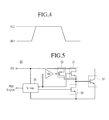
- FIG. 5 is a circuit diagram of a gate driving apparatus according to the third embodiment.
- FIG. 6 is a view to explain an output waveform of a gate driving apparatus according to the third embodiment.
- an output terminal of a gate driving apparatus has a push-pull structure and the gate driving apparatus employs two NMOS elements or a PMOS element and an NMOS element.
- FIG. 1 shows an embodiment using two NMOS devices provided at an output terminal of the gate driving apparatus and
- FIG. 3 shows another embodiment using a PMOS device and an NMOS device.
- FIG. 1 is a circuit diagram of a gate driving apparatus according to the first embodiment.
- the gate driving apparatus 10 includes a first NMOS transistor 11, a second NMOS transistor 12, an IGBT 13 and a driver 14.
- the first NMOS transistor 11 is located higher than the second NMOS transistor 12.
- a drain terminal of the first NMOS transistor 11 is connected to a power supply terminal VCC and a source terminal of the first NMOS transistor 11 is connected to a drain terminal of the second NMOS transistor 12 and a gate terminal of the IGBT 13.
- a gate terminal of the first NMOS transistor 11 is connected to the driver 14.
- the second NMOS transistor 12 is located lower than the first NMOS transistor 11.
- the drain terminal of the second NMOS transistor 12 is connected to a source terminal of the first NMOS transistor 11 and the gate terminal of the IGBT 13.
- a source terminal of the second NMOS transistor 12 is grounded and a gate terminal of the second NMOS transistor 12 is connected to the driver 14.
- An emitter terminal of the IGBT 13 is grounded and the gate terminal of the IGBT 13 is connected to the source terminal of the first NMOS transistor 11 and the drain terminal of the second NMOS transistor 12.
- the gate driving apparatus 10 amplifies a switching signal generated from the driver 14.
- a signal having intensity the same as that of a signal output from the driver 14 and a phase opposite to that of the signal output from the driver 14 is input into the gate terminal of the first NMOS transistor 11.
- the signal output from the driver 14 is input into the gate terminal of the second NMOS transistor 12 and the second NMOS transistor 12 outputs an amplified gate switching signal to drive the gate of the IGBT 13.
- the driver 14 drives the gate driving apparatus 10 and can prevent the arm short by setting a dead time upon the operation of the first and second NMOS transistors 11 and 12.
- the dead time signifies a time during which the other switching device is not turned on until one switching device is completely turned off. If the dead time is not set in the switching device, two switching devices may be simultaneously turned on, so excessive current may flow in a short period of time, so that the efficiency is lowered and the switching devices are damaged.
- the gate driving apparatus 10 In a state that the operating power is applied to the power supply terminal VCC, the gate driving apparatus 10 outputs the switching signal according to a control signal input thereto from a control unit (not shown). If the IGBT 13 is turned on, the first NMOS transistor 11 is turned on and the second NMOS transistor 12 is turned off. After that, the gate capacitance of the IGBT 13 is charged by the first NMOS transistor 11 so that the gate voltage rises. If the IGBT 13 is turned off, the first NMOS transistor 11 is turned off and the second NMOS transistor 12 is turned on and the gate capacitance of the IGBT 13 is discharged by the first NMOS transistor 11 so that the gate voltage drops.
- FIG. 2 is a view to explain an output waveform of the first NMOS transistor of the gate driving apparatus according to the first embodiment.
- An on-resistance value of the first NMOS transistor 11 is low, so the first NMOS transistor 11 is advantageous to drive high current.
- the predetermined value is calculated by subtracting threshold voltage Vth from power supply voltage VCC (VCC-Vth)
- VCC-Vth power supply voltage
- the voltage drop may occur to the extent of the threshold voltage based on the power supply voltage VCC.
- a switching device such as the IGBT, must have gate driving voltage having a predetermined level or more. Otherwise, the turn-on loss of the switching device is increased so that the efficiency is lowered and the life span of the switching device is shortened. In order to prevent the voltage drop, power supply voltage is increased corresponding to the voltage drop, causing great power consumption of the gate driving apparatus.
- FIG. 3 is a circuit diagram of the gate driving apparatus according to the second embodiment.
- the gate driving apparatus 20 includes a PMOS transistor 21, an NMOS transistor 22, an IGBT 23 and a driver 24.
- the PMOS transistor 21 is located higher than the NMOS transistor 22.
- a source terminal of the PMOS transistor 21 is connected to a power supply terminal VCC and a drain terminal of the PMOS transistor 21 is connected to a drain terminal of the NMOS transistor 22 and a gate terminal of the IGBT 23.
- a gate terminal of the PMOS transistor 21 is connected to the driver 24.
- the NMOS transistor 22 is located lower than the PMOS transistor 21.
- the drain terminal of the NMOS transistor 22 is connected to the drain terminal of the PMOS transistor 21 and the gate terminal of the IGBT 23.
- a source terminal of the NMOS transistor 22 is grounded and a gate terminal of the NMOS transistor 22 is connected to the driver 24.
- An emitter terminal of the IGBT 23 is grounded and the gate terminal of the IGBT 23 is connected to the drain terminal of the PMOS transistor 21 and the drain terminal of the NMOS transistor 22.
- the gate driving apparatus 20 amplifies a switching signal generated from the driver 24.
- a signal output from the driver 24 is input into the gate terminal of the PMOS transistor 21.
- the signal output from the driver 24 is input into the gate terminal of the NMOS transistor 22 and the NMOS transistor 22 outputs an amplified gate switching signal to drive the gate of the IGBT 23.
- the driver 24 drives the gate driving apparatus 20 and can prevent the arm short by setting a dead time upon the operation of the PMOS and NMOS transistors 21 and 22.
- the gate driving apparatus 20 In a state that the operating power is applied to the power supply terminal VCC, the gate driving apparatus 20 outputs the switching signal according to a control signal input thereto from a control unit (not shown). If the IGBT 23 is turned on, the PMOS transistor 21 is turned on and the NMOS transistor 22 is turned off. Therefore, the gate capacitance of the IGBT 23 is charged by the PMOS transistor 21 so that the gate voltage rises. If the IGBT 23 is turned off, the PMOS transistor 21 is turned off and the NMOS transistor 22 is turned on and the gate capacitance of the IGBT 23 is discharged by the NMOS transistor 22 so that the gate voltage drops.
- FIG. 4 is a view to explain an output waveform of the PMOS transistor of the gate driving apparatus according to the second embodiment.
- the output waveform of the PMOS transistor 21 has no voltage drop which occurs in the output terminal of the gate driving apparatus 10 shown in FIG. 1 .
- the output voltage of the PMOS transistor 21 may rise up to the power supply voltage VCC.
- the resistance value when the PMOS transistor 21 is turned on is higher than the resistance value when the NMOS transistor 22 is turned on, the chip size may become enlarged although the same current capacitance is driven so that the chip manufacturing cost may be increased.
- FIG. 5 is a circuit diagram of a gate driving apparatus according to the third embodiment.
- the gate driving apparatus 30 includes a first NMOS transistor 31, a second NMOS transistor 32, a PMOS transistor 33, an IGBT 34 and a driver 35.
- the first NMOS transistor 31 is located higher than the second NMOS transistor 32.
- a drain terminal of the first NMOS transistor 31 is connected to a power supply terminal VCC and a gate terminal of the PMOS transistor 33, a source terminal of the first NMOS transistor 31 is connected to a drain terminal of the second NMOS transistor 32, a gate terminal of the IGBT 34, and a drain terminal of the PMOS transistor 33.
- a gate terminal of the first NMOS transistor 31 is connected to the driver 35.
- the second NMOS transistor 32 is located lower than the first NMOS transistor 31.
- the drain terminal of the second NMOS transistor 32 is connected to the source terminal of the first NMOS transistor 31, the gate terminal of the IGBT 34, and the drain terminal of the PMOS transistor 33.
- a source terminal of the second NMOS transistor 32 is grounded and a gate terminal of the second NMOS transistor 32 is connected to the driver 35.
- the PMOS transistor 33 may be connected to the first NMOS transistor 31 in parallel.
- a source terminal of the PMOS transistor 33 is connected to the power supply terminal VCC
- the drain terminal of the PMOS transistor 33 is connected to the source terminal of the first NMOS transistor 31, the drain terminal of the second NMOS transistor 32 and the gate terminal of the IGBT 34.
- a gate terminal of the PMOS transistor 33 is connected to the driver 35.
- An emitter terminal of the IGBT 34 is grounded and the gate terminal of the IGBT 34 is connected to the source terminal of the first NMOS transistor 31, the drain terminal of the second NMOS transistor 32 and the drain terminal of the PMOS transistor 33.
- the driver 35 receives the PWM signal from the outside to drive the IGBT 34 by supplying current to the gate of the IGBT 34.
- a signal having intensity the same as that of a signal output from the driver 35 and a phase opposite to that of the signal output from the driver 35 is input into the gate terminal of the first NMOS transistor 31 and the first NMOS transistor 31 transfers the signal to the gate terminal of the IGBT 34.
- the first NMOS transistor 31 can amplify the current of the signal output from the driver 35.
- the PMOS transistor 33 receives the signal output from the driver 35 through the gate terminal and transfers the signal to the gate terminal of the IGBT 34.
- the first NMOS transistor 31 and the PMOS transistor 33 may charge the gate capacitance of the IGBT 34.
- the gate capacitance refers to parasitic capacitance generated from the IGBT 34 itself.
- the second NMOS transistor 32 may discharge the gate capacitance of the IGBT 34.
- the gate capacitance of the IGBT 34 may be charged through the turn-on of the first NMOS transistor 31 and the PMOS transistor 33 and the turn-off of the second NMOS transistor 32 and may be discharged through the turn-off of the first NMOS transistor 31 and the PMOS transistor 33 and the turn-on of the second NMOS transistor 32. That is, the gate capacitance of the IGBT 34 may be charged or discharged through the operation of the three switching devices so that the IGBT 34 can be driven.
- the IGBT 34 is connected to a motor and a load to serve as a switching device.
- the gate driving apparatus 30 may further include a control unit (not shown) that outputs driving signals for the first NMOS transistor 31, the second NMOS transistor 32 and the IGBT 34.
- the driving signal may be a turn-on signal or a turn-off signal.
- the driver 35 drives the gate driving apparatus 30 and can prevent the arm short by setting a dead time upon the operation of the first and second NMOS transistors 31 and 32.
- the dead time signifies a time during which the other switching device is not turned on until one switching device is completely turned off. If the dead time is not set in the switching device, two switching devices may be simultaneously turned on, so excessive current may flow in a short period of time, so that the efficiency is lowered and the switching devices are damaged.
- the time value of the dead time may be preset when the gate driving apparatus 30 is designed, but the embodiment is not limited thereto.
- the time value of the dead time may vary depending on the setting of the user.
- FIG. 6 is a view to explain an output waveform of the gate driving apparatus according to the third embodiment.
- the turn-off signal is input into the gate terminal of the first NMOS transistor 31 and the gate terminal of the PMOS transistor 33 and the turn-on signal is input into the gate terminal of the second NMOS transistor 32, so the output voltage of the gate driving apparatus 30 is maintained at 0 V.
- the turn-on signal is input into the gate terminal of the first NMOS transistor 31 and the gate terminal of the PMOS transistor 33 and the turn-off signal is input into the gate terminal of the second NMOS transistor 32, so the output voltage of the gate driving apparatus 30 rises rapidly.
- a B section shows the output waveform of the gate driving apparatus 30 in a state that the turn-off signal is being input into the gate terminal of the first NMOS transistor 31 and the gate terminal of the PMOS transistor 33.
- the output voltage of the first NMOS transistor 31 rises, the voltage between the gate terminal and the source terminal of the first NMOS transistor 31 becomes lower than the threshold voltage Vth, so the first NMOS transistor 31 is turned off.
- the PMOS transistor 33 is still turned on while charging the gate capacitance of the IGBT, so the output voltage of the gate driving apparatus 30 may reach the power supply voltage Vcc.
- the output voltage of the gate driving apparatus 30 may reach the power supply voltage Vcc, so the damage to the switching device caused by the output voltage drop can be prevented.
Landscapes
- Engineering & Computer Science (AREA)
- Power Engineering (AREA)
- Power Conversion In General (AREA)
Abstract
Description
- The embodiment relates to a gate driving apparatus for driving an IGBT (insulated gate bipolar mode transistor) in a power semiconductor system. More particularly, the embodiment relates to a gate driving apparatus having an improved output terminal structure for driving an IGBT in a power semiconductor system.
- In general, an inverter is extensively used in various industrial fields, such as a field of a motor and various electronic appliances. The inverter is a device to convert DC voltage into AC voltage and includes a switching device and a gate driving apparatus for driving the switching device in order to DC voltage into AC voltage.
- The IGBT is extensively used as a switching device for driving the gate driving apparatus. The IGBT is a transistor including emitter, collector and gate terminals, in which the gate terminal is insulated. The IGBT has high input impedance, so the IGBT can be readily and simply driven and minority carriers are not accumulated in the IGBT. That is, the IGBT is a switching device having the advantage of a MOSFET (metal oxide film field effect transistor) that operates at the high speed as well as the advantage of a BJT (bipolar transistor) that generates high current and is fabricated at an inexpensive cost. Since the IGBT has great input capacitance, the inverter requires a gate driving apparatus to drive a gate by amplifying current of a PWM (pulse width modulation) signal.
- However, the gate driving apparatus according to the related art has the structural feature suitable for high output voltage and a chip size may be enlarged, so that the chip cost is expensive.
- The embodiment provides a gate driving apparatus capable of preventing output voltage drop while reducing a chip size by connecting an NMOS and a PMOS to an upper portion of an output terminal of the gate driving apparatus in parallel and connecting an NMOS to a lower portion of the output terminal of the gate driving apparatus.
- A gate driving apparatus according to the embodiment may include a first switching device, a second switching device that outputs a signal to charge a capacitance of the first switching device, a third switching device connected in parallel to the second switching device to prevent a drop of a voltage output from the second switching device, and a fourth switching device that outputs a signal to discharge the capacitance of the first switching device.
- The first switching device may be an insulated gate bipolar transistor, the second and fourth switching devices may be NMOS transistors and the third switching device may be a PMOS transistor.
- The gate driving apparatus may further include a driver that receives a pulse width modulation signal to drive the first switching device by supplying a current to the first switching device.
- The driver may drive the second switching device and the fourth switching device while setting a dead time.
- The driver may turn on the second and third switching devices and turn off the fourth switching device.
- The driver may turn off the second and third switching devices and turn on the fourth switching device.
- The first switching device may be an insulated gate bipolar transistor and the capacitance of the first switching device may be a gate capacitance of the insulated gate bipolar transistor.
- The capacitance of the first switching device may be a parasitic capacitance generated in the first switching device.
- A gate driving apparatus according to another embodiment may include a first NMOS transistor, a second NMOS transistor, a PMOS transistor and an insulated gate bipolar transistor.
- A drain terminal of the first NMOS transistor may be connected to a terminal of a power source and the PMOS transistor, a gate terminal of the first NMOS transistor may be connected to a driver, and a source terminal of the first NMOS transistor may be connected to a drain terminal of the PMOS transistor, a drain terminal of the second NMOS transistor and a gate terminal of the insulated gate bipolar transistor. A gate terminal of the PMOS transistor may be connected to the driver, a gate terminal of the second NMOS transistor may be connected to the driver, and a source terminal of the second NMOS transistor and an emitter terminal of the insulated gate bipolar transistor may be grounded.
- The PMOS transistor may drop an output voltage of the first NMOS transistor.
- The driver may turn on the first NMOS transistor and the PMOS transistor and turn off the second NMOS transistor to charge a gate capacitance of the insulated gate bipolar transistor.
- The driver may turn off the first NMOS transistor and the PMOS transistor and turn on the second NMOS transistor to discharge a gate capacitance of the insulated gate bipolar transistor.
- The driver may prevent an arm short among the first NMOS transistor, the PMOS transistor and the second NMOS transistor by setting a dead time.
- According to the embodiment, the NMOS transistor is used as the main switching device and the PMOS transistor connected in parallel to the NMOS transistor is used as the sub-switching device, so that the chip size can be reduced without dropping the output voltage of the gate driving apparatus.
- In addition, according to the embodiment, the loss of the switching device can be prevented by preventing the output voltage of the gate driving apparatus from being dropped.
- Meanwhile, other various effects will be directly or indirectly disclosed in the detailed description of the embodiment.
-
FIG. 1 is a circuit diagram of a gate driving apparatus according to the first embodiment; -
FIG. 2 is a view to explain an output waveform of a first NMOS transistor of a gate driving apparatus according to the first embodiment; -
FIG. 3 is a circuit diagram of a gate driving apparatus according to the second embodiment; -
FIG. 4 is a view to explain an output waveform of a PMOS transistor of a gate driving apparatus according to the second embodiment; -
FIG. 5 is a circuit diagram of a gate driving apparatus according to the third embodiment; and -
FIG. 6 is a view to explain an output waveform of a gate driving apparatus according to the third embodiment. - Hereinafter, embodiments will be described in detail with reference to accompanying drawings so that those skilled in the art can easily work with the embodiments.
- In a power semiconductor system, an output terminal of a gate driving apparatus has a push-pull structure and the gate driving apparatus employs two NMOS elements or a PMOS element and an NMOS element.
-
FIG. 1 shows an embodiment using two NMOS devices provided at an output terminal of the gate driving apparatus andFIG. 3 shows another embodiment using a PMOS device and an NMOS device. -
FIG. 1 is a circuit diagram of a gate driving apparatus according to the first embodiment. - Referring to
FIG. 1 , thegate driving apparatus 10 includes afirst NMOS transistor 11, asecond NMOS transistor 12, anIGBT 13 and adriver 14. - The
first NMOS transistor 11 is located higher than thesecond NMOS transistor 12. A drain terminal of thefirst NMOS transistor 11 is connected to a power supply terminal VCC and a source terminal of thefirst NMOS transistor 11 is connected to a drain terminal of thesecond NMOS transistor 12 and a gate terminal of theIGBT 13. A gate terminal of thefirst NMOS transistor 11 is connected to thedriver 14. - The
second NMOS transistor 12 is located lower than thefirst NMOS transistor 11. The drain terminal of thesecond NMOS transistor 12 is connected to a source terminal of thefirst NMOS transistor 11 and the gate terminal of theIGBT 13. A source terminal of thesecond NMOS transistor 12 is grounded and a gate terminal of thesecond NMOS transistor 12 is connected to thedriver 14. - An emitter terminal of the
IGBT 13 is grounded and the gate terminal of theIGBT 13 is connected to the source terminal of thefirst NMOS transistor 11 and the drain terminal of thesecond NMOS transistor 12. - The
gate driving apparatus 10 amplifies a switching signal generated from thedriver 14. - A signal having intensity the same as that of a signal output from the
driver 14 and a phase opposite to that of the signal output from thedriver 14 is input into the gate terminal of thefirst NMOS transistor 11. - The signal output from the
driver 14 is input into the gate terminal of thesecond NMOS transistor 12 and thesecond NMOS transistor 12 outputs an amplified gate switching signal to drive the gate of theIGBT 13. - The
driver 14 drives thegate driving apparatus 10 and can prevent the arm short by setting a dead time upon the operation of the first andsecond NMOS transistors - In a state that the operating power is applied to the power supply terminal VCC, the
gate driving apparatus 10 outputs the switching signal according to a control signal input thereto from a control unit (not shown). If theIGBT 13 is turned on, thefirst NMOS transistor 11 is turned on and thesecond NMOS transistor 12 is turned off. After that, the gate capacitance of theIGBT 13 is charged by thefirst NMOS transistor 11 so that the gate voltage rises. If theIGBT 13 is turned off, thefirst NMOS transistor 11 is turned off and thesecond NMOS transistor 12 is turned on and the gate capacitance of theIGBT 13 is discharged by thefirst NMOS transistor 11 so that the gate voltage drops. -
FIG. 2 is a view to explain an output waveform of the first NMOS transistor of the gate driving apparatus according to the first embodiment. - An on-resistance value of the
first NMOS transistor 11 is low, so thefirst NMOS transistor 11 is advantageous to drive high current. However, as shown inFIG. 2 , if output voltage rises by a predetermined value or more, in which the predetermined value is calculated by subtracting threshold voltage Vth from power supply voltage VCC (VCC-Vth), the voltage drop may occur to the extent of the threshold voltage based on the power supply voltage VCC. A switching device, such as the IGBT, must have gate driving voltage having a predetermined level or more. Otherwise, the turn-on loss of the switching device is increased so that the efficiency is lowered and the life span of the switching device is shortened. In order to prevent the voltage drop, power supply voltage is increased corresponding to the voltage drop, causing great power consumption of the gate driving apparatus. -
FIG. 3 is a circuit diagram of the gate driving apparatus according to the second embodiment. - Referring to
FIG. 2 , thegate driving apparatus 20 includes aPMOS transistor 21, anNMOS transistor 22, anIGBT 23 and adriver 24. - The
PMOS transistor 21 is located higher than theNMOS transistor 22. A source terminal of thePMOS transistor 21 is connected to a power supply terminal VCC and a drain terminal of thePMOS transistor 21 is connected to a drain terminal of theNMOS transistor 22 and a gate terminal of theIGBT 23. A gate terminal of thePMOS transistor 21 is connected to thedriver 24. - The
NMOS transistor 22 is located lower than thePMOS transistor 21. The drain terminal of theNMOS transistor 22 is connected to the drain terminal of thePMOS transistor 21 and the gate terminal of theIGBT 23. A source terminal of theNMOS transistor 22 is grounded and a gate terminal of theNMOS transistor 22 is connected to thedriver 24. - An emitter terminal of the
IGBT 23 is grounded and the gate terminal of theIGBT 23 is connected to the drain terminal of thePMOS transistor 21 and the drain terminal of theNMOS transistor 22. - The
gate driving apparatus 20 amplifies a switching signal generated from thedriver 24. - A signal output from the
driver 24 is input into the gate terminal of thePMOS transistor 21. - The signal output from the
driver 24 is input into the gate terminal of theNMOS transistor 22 and theNMOS transistor 22 outputs an amplified gate switching signal to drive the gate of theIGBT 23. - The
driver 24 drives thegate driving apparatus 20 and can prevent the arm short by setting a dead time upon the operation of the PMOS andNMOS transistors - In a state that the operating power is applied to the power supply terminal VCC, the
gate driving apparatus 20 outputs the switching signal according to a control signal input thereto from a control unit (not shown). If theIGBT 23 is turned on, thePMOS transistor 21 is turned on and theNMOS transistor 22 is turned off. Therefore, the gate capacitance of theIGBT 23 is charged by thePMOS transistor 21 so that the gate voltage rises. If theIGBT 23 is turned off, thePMOS transistor 21 is turned off and theNMOS transistor 22 is turned on and the gate capacitance of theIGBT 23 is discharged by theNMOS transistor 22 so that the gate voltage drops. -
FIG. 4 is a view to explain an output waveform of the PMOS transistor of the gate driving apparatus according to the second embodiment. - Referring to
FIG. 4 , the output waveform of thePMOS transistor 21 has no voltage drop which occurs in the output terminal of thegate driving apparatus 10 shown inFIG. 1 . Thus, the output voltage of thePMOS transistor 21 may rise up to the power supply voltage VCC. - However, the resistance value when the
PMOS transistor 21 is turned on is higher than the resistance value when theNMOS transistor 22 is turned on, the chip size may become enlarged although the same current capacitance is driven so that the chip manufacturing cost may be increased. -
FIG. 5 is a circuit diagram of a gate driving apparatus according to the third embodiment. - Referring to
FIG. 5 , thegate driving apparatus 30 includes afirst NMOS transistor 31, asecond NMOS transistor 32, aPMOS transistor 33, anIGBT 34 and adriver 35. - The
first NMOS transistor 31 is located higher than thesecond NMOS transistor 32. - A drain terminal of the
first NMOS transistor 31 is connected to a power supply terminal VCC and a gate terminal of thePMOS transistor 33, a source terminal of thefirst NMOS transistor 31 is connected to a drain terminal of thesecond NMOS transistor 32, a gate terminal of theIGBT 34, and a drain terminal of thePMOS transistor 33. A gate terminal of thefirst NMOS transistor 31 is connected to thedriver 35. - The
second NMOS transistor 32 is located lower than thefirst NMOS transistor 31. The drain terminal of thesecond NMOS transistor 32 is connected to the source terminal of thefirst NMOS transistor 31, the gate terminal of theIGBT 34, and the drain terminal of thePMOS transistor 33. A source terminal of thesecond NMOS transistor 32 is grounded and a gate terminal of thesecond NMOS transistor 32 is connected to thedriver 35. - The
PMOS transistor 33 may be connected to thefirst NMOS transistor 31 in parallel. In detail, a source terminal of thePMOS transistor 33 is connected to the power supply terminal VCC, the drain terminal of thePMOS transistor 33 is connected to the source terminal of thefirst NMOS transistor 31, the drain terminal of thesecond NMOS transistor 32 and the gate terminal of theIGBT 34. A gate terminal of thePMOS transistor 33 is connected to thedriver 35. - An emitter terminal of the
IGBT 34 is grounded and the gate terminal of theIGBT 34 is connected to the source terminal of thefirst NMOS transistor 31, the drain terminal of thesecond NMOS transistor 32 and the drain terminal of thePMOS transistor 33. - The
driver 35 receives the PWM signal from the outside to drive theIGBT 34 by supplying current to the gate of theIGBT 34. - A signal having intensity the same as that of a signal output from the
driver 35 and a phase opposite to that of the signal output from thedriver 35 is input into the gate terminal of thefirst NMOS transistor 31 and thefirst NMOS transistor 31 transfers the signal to the gate terminal of theIGBT 34. - The
first NMOS transistor 31 can amplify the current of the signal output from thedriver 35. - The
PMOS transistor 33 receives the signal output from thedriver 35 through the gate terminal and transfers the signal to the gate terminal of theIGBT 34. - The
first NMOS transistor 31 and thePMOS transistor 33 may charge the gate capacitance of theIGBT 34. The gate capacitance refers to parasitic capacitance generated from theIGBT 34 itself. - The
second NMOS transistor 32 may discharge the gate capacitance of theIGBT 34. - The gate capacitance of the
IGBT 34 may be charged through the turn-on of thefirst NMOS transistor 31 and thePMOS transistor 33 and the turn-off of thesecond NMOS transistor 32 and may be discharged through the turn-off of thefirst NMOS transistor 31 and thePMOS transistor 33 and the turn-on of thesecond NMOS transistor 32. That is, the gate capacitance of theIGBT 34 may be charged or discharged through the operation of the three switching devices so that theIGBT 34 can be driven. - The
IGBT 34 is connected to a motor and a load to serve as a switching device. - The
gate driving apparatus 30 may further include a control unit (not shown) that outputs driving signals for thefirst NMOS transistor 31, thesecond NMOS transistor 32 and theIGBT 34. The driving signal may be a turn-on signal or a turn-off signal. - The
driver 35 drives thegate driving apparatus 30 and can prevent the arm short by setting a dead time upon the operation of the first andsecond NMOS transistors - According to one embodiment, the time value of the dead time may be preset when the
gate driving apparatus 30 is designed, but the embodiment is not limited thereto. The time value of the dead time may vary depending on the setting of the user. -
FIG. 6 is a view to explain an output waveform of the gate driving apparatus according to the third embodiment. - Referring to
FIG. 6 , before an A section of the output waveform, the turn-off signal is input into the gate terminal of thefirst NMOS transistor 31 and the gate terminal of thePMOS transistor 33 and the turn-on signal is input into the gate terminal of thesecond NMOS transistor 32, so the output voltage of thegate driving apparatus 30 is maintained at 0 V. - In the A section, the turn-on signal is input into the gate terminal of the
first NMOS transistor 31 and the gate terminal of thePMOS transistor 33 and the turn-off signal is input into the gate terminal of thesecond NMOS transistor 32, so the output voltage of thegate driving apparatus 30 rises rapidly. - A B section shows the output waveform of the
gate driving apparatus 30 in a state that the turn-off signal is being input into the gate terminal of thefirst NMOS transistor 31 and the gate terminal of thePMOS transistor 33. In this case, as the output voltage of thefirst NMOS transistor 31 rises, the voltage between the gate terminal and the source terminal of thefirst NMOS transistor 31 becomes lower than the threshold voltage Vth, so thefirst NMOS transistor 31 is turned off. However, thePMOS transistor 33 is still turned on while charging the gate capacitance of the IGBT, so the output voltage of thegate driving apparatus 30 may reach the power supply voltage Vcc. - As described above, according to the third embodiment, the output voltage of the
gate driving apparatus 30 may reach the power supply voltage Vcc, so the damage to the switching device caused by the output voltage drop can be prevented. - Although embodiments have been described with reference to a number of illustrative embodiments thereof, it should be understood that numerous other modifications and embodiments can be devised by those skilled in the art that will fall within the spirit and scope of the principles of this disclosure.
More particularly, various variations and modifications are possible in the component parts and/or arrangements of the subject combination arrangement within the scope of the disclosure, the drawings and the appended claims. In addition to variations and modifications in the component parts and/or arrangements, alternative uses will also be apparent to those skilled in the art.
Claims (13)
- A gate driving apparatus comprising:a first switching device;a second switching device that outputs a signal to charge a capacitance of the first switching device;a third switching device connected in parallel to the second switching device to prevent a drop of a voltage output from the second switching device; anda fourth switching device that outputs a signal to discharge the capacitance of the first switching device.
- The gate driving apparatus of claim 1, further comprising a driver that receives a pulse width modulation signal to drive the first switching device by supplying a current to the first switching device.
- The gate driving apparatus of claim 3, wherein the driver drives the second switching device and the fourth switching device while setting a dead time.
- The gate driving apparatus of claim 3, wherein the driver turns on the second and third switching devices and turns off the fourth switching device.
- The gate driving apparatus of claim 3, wherein the driver turns off the second and third switching devices and turns on the fourth switching device.
- The gate driving apparatus according to one of the claims 1 to 5, wherein the first switching device is an insulated gate bipolar transistor, the second and fourth switching devices are NMOS transistors and the third switching device is a PMOS transistor.
- The gate driving apparatus according to one of the claims 1 to 5, wherein the first switching device is an insulated gate bipolar transistor and the capacitance of the first switching device is a gate capacitance of the insulated gate bipolar transistor.
- The gate driving apparatus of claim 1, wherein the capacitance of the first switching device is a parasitic capacitance generated in the first switching device.
- A gate driving apparatus including a power source and a driver, the gate driving comprising:a first NMOS transistor;a second NMOS transistor;a PMOS transistor; andan insulated gate bipolar transistor,wherein a drain terminal of the first NMOS transistor is connected to a terminal of the power source and the PMOS transistor, a gate terminal of the first NMOS transistor is connected to the driver, and a source terminal of the first NMOS transistor is connected to a drain terminal of the PMOS transistor, a drain terminal of the second NMOS transistor and a gate terminal of the insulated gate bipolar transistor,a gate terminal of the PMOS transistor is connected to the driver,a gate terminal of the second NMOS transistor is connected to the driver, anda source terminal of the second NMOS transistor and an emitter terminal of the insulated gate bipolar transistor are grounded.
- The gate driving apparatus of claim 9, wherein the PMOS transistor drops an output voltage of the first NMOS transistor.
- The gate driving apparatus of claim 9, wherein the driver turns on the first NMOS transistor and the PMOS transistor and turns off the second NMOS transistor to charge a gate capacitance of the insulated gate bipolar transistor.
- The gate driving apparatus of claim 9, wherein the driver turns off the first NMOS transistor and the PMOS transistor and turns on the second NMOS transistor to discharge a gate capacitance of the insulated gate bipolar transistor.
- The gate driving apparatus of claim 9, wherein the driver prevents an arm short among the first NMOS transistor, the PMOS transistor and the second NMOS transistor by setting a dead time.
Applications Claiming Priority (1)
| Application Number | Priority Date | Filing Date | Title |
|---|---|---|---|
| KR1020120042883A KR101297460B1 (en) | 2012-04-24 | 2012-04-24 | Apparatus for driving gate |
Publications (2)
| Publication Number | Publication Date |
|---|---|
| EP2658127A2 true EP2658127A2 (en) | 2013-10-30 |
| EP2658127A3 EP2658127A3 (en) | 2014-09-03 |
Family
ID=48045339
Family Applications (1)
| Application Number | Title | Priority Date | Filing Date |
|---|---|---|---|
| EP13162705.1A Withdrawn EP2658127A3 (en) | 2012-04-24 | 2013-04-08 | Gate driving apparatus |
Country Status (5)
| Country | Link |
|---|---|
| US (1) | US8760200B2 (en) |
| EP (1) | EP2658127A3 (en) |
| JP (1) | JP5698299B2 (en) |
| KR (1) | KR101297460B1 (en) |
| CN (1) | CN103378714A (en) |
Cited By (1)
| Publication number | Priority date | Publication date | Assignee | Title |
|---|---|---|---|---|
| EP4037186A4 (en) * | 2019-09-27 | 2022-11-23 | Tamura Corporation | GRID ATTACK CIRCUIT |
Families Citing this family (9)
| Publication number | Priority date | Publication date | Assignee | Title |
|---|---|---|---|---|
| WO2015079882A1 (en) * | 2013-11-29 | 2015-06-04 | 日産自動車株式会社 | Switching device |
| EP3068022B1 (en) | 2015-03-13 | 2019-03-06 | Nxp B.V. | Discharging an input capacitor of a switch mode power supply |
| CN105048790B (en) * | 2015-07-22 | 2017-12-05 | 深圳市稳先微电子有限公司 | Power tube control system and the drive circuit for driving external power tube |
| CN108599750A (en) * | 2018-01-23 | 2018-09-28 | 电子科技大学 | A kind of single supply driving circuit of SiC-BJT |
| JP2019134622A (en) * | 2018-02-01 | 2019-08-08 | ローム株式会社 | Driver circuit and switching regulator |
| CN117424585A (en) * | 2019-12-30 | 2024-01-19 | 上海瞻芯电子科技有限公司 | Gate driving device and electronic equipment |
| US11599760B2 (en) | 2020-06-25 | 2023-03-07 | Samsung Electronics Co., Ltd. | Bi-directional voltage converter of smart card and smart card including the same |
| US12212224B2 (en) * | 2020-12-25 | 2025-01-28 | Fuji Electric Co., Ltd. | Driving apparatus |
| CN115102371B (en) * | 2022-05-20 | 2026-03-17 | 昂宝集成电路股份有限公司 | Switching power supply control circuit and method |
Family Cites Families (25)
| Publication number | Priority date | Publication date | Assignee | Title |
|---|---|---|---|---|
| JPH03169273A (en) * | 1989-11-22 | 1991-07-22 | Mitsubishi Electric Corp | Drive circuit for switching device |
| US5010261A (en) * | 1989-12-08 | 1991-04-23 | General Electric Company | Lossless gate driver circuit for a high frequency converter |
| JP3337796B2 (en) * | 1993-11-17 | 2002-10-21 | 東洋電機製造株式会社 | Drive circuit for voltage-driven elements |
| JP3123349B2 (en) * | 1994-06-29 | 2001-01-09 | 富士電機株式会社 | Control circuit for semiconductor device |
| JP3430878B2 (en) * | 1997-09-19 | 2003-07-28 | 富士電機株式会社 | MOS gate type element driving circuit |
| JP3047869B2 (en) * | 1997-09-26 | 2000-06-05 | 日本電気株式会社 | Output amplitude adjustment circuit |
| US6133757A (en) * | 1998-07-16 | 2000-10-17 | Via Technologies, Inc. | High-speed and low-noise output buffer |
| JP3666843B2 (en) * | 1999-02-26 | 2005-06-29 | 株式会社東芝 | Gate circuit of insulated gate semiconductor device |
| JP2001223571A (en) * | 2000-02-10 | 2001-08-17 | Fuji Electric Co Ltd | Gate drive device for voltage driven semiconductor device |
| JP2005045590A (en) * | 2003-07-23 | 2005-02-17 | Mitsubishi Electric Corp | Semiconductor device |
| US20060192437A1 (en) * | 2003-08-01 | 2006-08-31 | Koninklijke Philips Electronics N.V. | High frequency control of a semiconductor switch |
| US7598792B2 (en) * | 2005-01-31 | 2009-10-06 | Queen's University At Kingston | Resonant gate drive circuits |
| JP4952112B2 (en) * | 2006-07-24 | 2012-06-13 | サンケン電気株式会社 | Drive circuit for voltage-driven element |
| JP4909684B2 (en) * | 2006-09-06 | 2012-04-04 | 三菱電機株式会社 | Semiconductor device |
| KR100807541B1 (en) * | 2006-09-29 | 2008-02-29 | 엘에스산전 주식회사 | Gate driving circuit of power semiconductor switch |
| JP2008306618A (en) * | 2007-06-11 | 2008-12-18 | Nissan Motor Co Ltd | Driving circuit for driving a voltage driven element |
| JP4682173B2 (en) * | 2007-07-12 | 2011-05-11 | 株式会社日立製作所 | Voltage-driven semiconductor element drive circuit and inverter device |
| JP5145142B2 (en) * | 2008-07-08 | 2013-02-13 | パナソニック株式会社 | Half bridge circuit |
| JP5284077B2 (en) * | 2008-12-26 | 2013-09-11 | 株式会社日立製作所 | Semiconductor device and power conversion device using the same |
| JP5487922B2 (en) * | 2009-03-09 | 2014-05-14 | サンケン電気株式会社 | Semiconductor device, driving method thereof, and driving device |
| JP5029678B2 (en) * | 2009-12-07 | 2012-09-19 | 株式会社デンソー | Driving device for switching element |
| JP2013038930A (en) * | 2011-08-08 | 2013-02-21 | Toshiba Corp | Switching circuit and dc-dc converter |
| JP5488550B2 (en) * | 2011-08-19 | 2014-05-14 | 株式会社安川電機 | Gate drive circuit and power conversion device |
| US8513937B2 (en) * | 2011-09-09 | 2013-08-20 | Micrel, Inc. | Switching regulator with optimized switch node rise time |
| JP5561352B2 (en) * | 2012-02-22 | 2014-07-30 | 株式会社デンソー | Driving circuit |
-
2012
- 2012-04-24 KR KR1020120042883A patent/KR101297460B1/en not_active Expired - Fee Related
-
2013
- 2013-04-04 US US13/857,056 patent/US8760200B2/en not_active Expired - Fee Related
- 2013-04-08 EP EP13162705.1A patent/EP2658127A3/en not_active Withdrawn
- 2013-04-15 JP JP2013084792A patent/JP5698299B2/en not_active Expired - Fee Related
- 2013-04-24 CN CN2013101457274A patent/CN103378714A/en active Pending
Non-Patent Citations (1)
| Title |
|---|
| None |
Cited By (2)
| Publication number | Priority date | Publication date | Assignee | Title |
|---|---|---|---|---|
| EP4037186A4 (en) * | 2019-09-27 | 2022-11-23 | Tamura Corporation | GRID ATTACK CIRCUIT |
| US11855612B2 (en) | 2019-09-27 | 2023-12-26 | Tamura Corporation | High-side driver |
Also Published As
| Publication number | Publication date |
|---|---|
| US8760200B2 (en) | 2014-06-24 |
| KR101297460B1 (en) | 2013-08-16 |
| CN103378714A (en) | 2013-10-30 |
| JP2013230081A (en) | 2013-11-07 |
| EP2658127A3 (en) | 2014-09-03 |
| US20130278322A1 (en) | 2013-10-24 |
| JP5698299B2 (en) | 2015-04-08 |
Similar Documents
| Publication | Publication Date | Title |
|---|---|---|
| US8760200B2 (en) | Gate driving apparatus | |
| US11611339B2 (en) | Power switch drive circuit and device | |
| US8362812B2 (en) | Switching gate driver | |
| CN106688183B (en) | Short circuit protection circuit for self-extinguishing semiconductor components | |
| CN205725692U (en) | For driving the gate driver circuit of power switch | |
| EP2015453B1 (en) | Drive circuit for voltage driven switching element | |
| US20080303580A1 (en) | Control circuit for a high-side semiconductor switch for switching a supply voltage | |
| US9331188B2 (en) | Short-circuit protection circuits, system, and method | |
| KR101202204B1 (en) | Power mosfet driver and method therefor | |
| CN102545559A (en) | Gate driver and semiconductor device employing the same | |
| CN102064729B (en) | Half-bridge drive circuit | |
| US11923832B1 (en) | Gate driver circuit with a limiting function to maintain control voltage under a rated limit | |
| CN104866000B (en) | Gate drive circuit and method with voltage regulator | |
| CN105024676B (en) | High-voltage bootstrap type grid driving device | |
| JP2018093681A (en) | DRIVE CIRCUIT AND SEMICONDUCTOR MODULE COMPRISING THE CIRCUIT | |
| CN104040890A (en) | Apparatus and method for control of semiconductor switching devices | |
| US20160134279A1 (en) | Method and circuit for recharging a bootstrap capacitor using a transfer capacitor | |
| CN107395000B (en) | Semiconductor device | |
| CN106464122A (en) | Gate driver controlling a collector to emitter voltage variation of an electronic switch and circuits including the gate driver | |
| KR101758808B1 (en) | Intelligent Power Module And Power Driving Module Thereof | |
| JP2019009914A (en) | Semiconductor device, power conversion device, drive device, vehicle, and elevator | |
| JP2009194514A (en) | Power semiconductor gate drive circuit | |
| CN109889026B (en) | Power device and electric appliance | |
| CN110289601B (en) | Active clamp circuit built into driver IC to protect IGBT | |
| US9768769B2 (en) | Power electronic device assembly for preventing parasitic switching-on of feeder circuit-breaker |
Legal Events
| Date | Code | Title | Description |
|---|---|---|---|
| PUAI | Public reference made under article 153(3) epc to a published international application that has entered the european phase |
Free format text: ORIGINAL CODE: 0009012 |
|
| AK | Designated contracting states |
Kind code of ref document: A2 Designated state(s): AL AT BE BG CH CY CZ DE DK EE ES FI FR GB GR HR HU IE IS IT LI LT LU LV MC MK MT NL NO PL PT RO RS SE SI SK SM TR |
|
| AX | Request for extension of the european patent |
Extension state: BA ME |
|
| PUAL | Search report despatched |
Free format text: ORIGINAL CODE: 0009013 |
|
| AK | Designated contracting states |
Kind code of ref document: A3 Designated state(s): AL AT BE BG CH CY CZ DE DK EE ES FI FR GB GR HR HU IE IS IT LI LT LU LV MC MK MT NL NO PL PT RO RS SE SI SK SM TR |
|
| AX | Request for extension of the european patent |
Extension state: BA ME |
|
| RIC1 | Information provided on ipc code assigned before grant |
Ipc: H03K 19/017 20060101ALN20140725BHEP Ipc: H03K 17/0412 20060101AFI20140725BHEP Ipc: H03K 17/06 20060101ALI20140725BHEP |
|
| 17P | Request for examination filed |
Effective date: 20141201 |
|
| RBV | Designated contracting states (corrected) |
Designated state(s): AL AT BE BG CH CY CZ DE DK EE ES FI FR GB GR HR HU IE IS IT LI LT LU LV MC MK MT NL NO PL PT RO RS SE SI SK SM TR |
|
| 17Q | First examination report despatched |
Effective date: 20160302 |
|
| STAA | Information on the status of an ep patent application or granted ep patent |
Free format text: STATUS: THE APPLICATION IS DEEMED TO BE WITHDRAWN |
|
| 18D | Application deemed to be withdrawn |
Effective date: 20171010 |