EP2654093B1 - Package and method for manufacturing package - Google Patents
Package and method for manufacturing package Download PDFInfo
- Publication number
- EP2654093B1 EP2654093B1 EP13163043.6A EP13163043A EP2654093B1 EP 2654093 B1 EP2654093 B1 EP 2654093B1 EP 13163043 A EP13163043 A EP 13163043A EP 2654093 B1 EP2654093 B1 EP 2654093B1
- Authority
- EP
- European Patent Office
- Prior art keywords
- electrode
- housing
- package
- light emitting
- emitting element
- Prior art date
- Legal status (The legal status is an assumption and is not a legal conclusion. Google has not performed a legal analysis and makes no representation as to the accuracy of the status listed.)
- Not-in-force
Links
Images


Classifications
-
- H—ELECTRICITY
- H10—SEMICONDUCTOR DEVICES; ELECTRIC SOLID-STATE DEVICES NOT OTHERWISE PROVIDED FOR
- H10H—INORGANIC LIGHT-EMITTING SEMICONDUCTOR DEVICES HAVING POTENTIAL BARRIERS
- H10H20/00—Individual inorganic light-emitting semiconductor devices having potential barriers, e.g. light-emitting diodes [LED]
- H10H20/80—Constructional details
- H10H20/83—Electrodes
- H10H20/831—Electrodes characterised by their shape
-
- H—ELECTRICITY
- H10—SEMICONDUCTOR DEVICES; ELECTRIC SOLID-STATE DEVICES NOT OTHERWISE PROVIDED FOR
- H10H—INORGANIC LIGHT-EMITTING SEMICONDUCTOR DEVICES HAVING POTENTIAL BARRIERS
- H10H20/00—Individual inorganic light-emitting semiconductor devices having potential barriers, e.g. light-emitting diodes [LED]
- H10H20/80—Constructional details
- H10H20/85—Packages
- H10H20/8506—Containers
-
- H—ELECTRICITY
- H10—SEMICONDUCTOR DEVICES; ELECTRIC SOLID-STATE DEVICES NOT OTHERWISE PROVIDED FOR
- H10H—INORGANIC LIGHT-EMITTING SEMICONDUCTOR DEVICES HAVING POTENTIAL BARRIERS
- H10H20/00—Individual inorganic light-emitting semiconductor devices having potential barriers, e.g. light-emitting diodes [LED]
- H10H20/80—Constructional details
- H10H20/85—Packages
- H10H20/857—Interconnections, e.g. lead-frames, bond wires or solder balls
-
- H—ELECTRICITY
- H10—SEMICONDUCTOR DEVICES; ELECTRIC SOLID-STATE DEVICES NOT OTHERWISE PROVIDED FOR
- H10H—INORGANIC LIGHT-EMITTING SEMICONDUCTOR DEVICES HAVING POTENTIAL BARRIERS
- H10H20/00—Individual inorganic light-emitting semiconductor devices having potential barriers, e.g. light-emitting diodes [LED]
- H10H20/80—Constructional details
- H10H20/85—Packages
- H10H20/858—Means for heat extraction or cooling
- H10H20/8582—Means for heat extraction or cooling characterised by their shape
-
- H—ELECTRICITY
- H01—ELECTRIC ELEMENTS
- H01L—SEMICONDUCTOR DEVICES NOT COVERED BY CLASS H10
- H01L2224/00—Indexing scheme for arrangements for connecting or disconnecting semiconductor or solid-state bodies and methods related thereto as covered by H01L24/00
- H01L2224/01—Means for bonding being attached to, or being formed on, the surface to be connected, e.g. chip-to-package, die-attach, "first-level" interconnects; Manufacturing methods related thereto
- H01L2224/42—Wire connectors; Manufacturing methods related thereto
- H01L2224/44—Structure, shape, material or disposition of the wire connectors prior to the connecting process
- H01L2224/45—Structure, shape, material or disposition of the wire connectors prior to the connecting process of an individual wire connector
- H01L2224/45001—Core members of the connector
- H01L2224/45099—Material
- H01L2224/451—Material with a principal constituent of the material being a metal or a metalloid, e.g. boron (B), silicon (Si), germanium (Ge), arsenic (As), antimony (Sb), tellurium (Te) and polonium (Po), and alloys thereof
- H01L2224/45138—Material with a principal constituent of the material being a metal or a metalloid, e.g. boron (B), silicon (Si), germanium (Ge), arsenic (As), antimony (Sb), tellurium (Te) and polonium (Po), and alloys thereof the principal constituent melting at a temperature of greater than or equal to 950°C and less than 1550°C
- H01L2224/45144—Gold (Au) as principal constituent
-
- H—ELECTRICITY
- H01—ELECTRIC ELEMENTS
- H01L—SEMICONDUCTOR DEVICES NOT COVERED BY CLASS H10
- H01L2224/00—Indexing scheme for arrangements for connecting or disconnecting semiconductor or solid-state bodies and methods related thereto as covered by H01L24/00
- H01L2224/01—Means for bonding being attached to, or being formed on, the surface to be connected, e.g. chip-to-package, die-attach, "first-level" interconnects; Manufacturing methods related thereto
- H01L2224/42—Wire connectors; Manufacturing methods related thereto
- H01L2224/47—Structure, shape, material or disposition of the wire connectors after the connecting process
- H01L2224/48—Structure, shape, material or disposition of the wire connectors after the connecting process of an individual wire connector
- H01L2224/4805—Shape
- H01L2224/4809—Loop shape
- H01L2224/48091—Arched
-
- H—ELECTRICITY
- H01—ELECTRIC ELEMENTS
- H01L—SEMICONDUCTOR DEVICES NOT COVERED BY CLASS H10
- H01L2224/00—Indexing scheme for arrangements for connecting or disconnecting semiconductor or solid-state bodies and methods related thereto as covered by H01L24/00
- H01L2224/73—Means for bonding being of different types provided for in two or more of groups H01L2224/10, H01L2224/18, H01L2224/26, H01L2224/34, H01L2224/42, H01L2224/50, H01L2224/63, H01L2224/71
- H01L2224/732—Location after the connecting process
- H01L2224/73251—Location after the connecting process on different surfaces
- H01L2224/73265—Layer and wire connectors
-
- H—ELECTRICITY
- H10—SEMICONDUCTOR DEVICES; ELECTRIC SOLID-STATE DEVICES NOT OTHERWISE PROVIDED FOR
- H10H—INORGANIC LIGHT-EMITTING SEMICONDUCTOR DEVICES HAVING POTENTIAL BARRIERS
- H10H20/00—Individual inorganic light-emitting semiconductor devices having potential barriers, e.g. light-emitting diodes [LED]
- H10H20/01—Manufacture or treatment
- H10H20/036—Manufacture or treatment of packages
- H10H20/0365—Manufacture or treatment of packages of means for heat extraction or cooling
-
- H—ELECTRICITY
- H10—SEMICONDUCTOR DEVICES; ELECTRIC SOLID-STATE DEVICES NOT OTHERWISE PROVIDED FOR
- H10H—INORGANIC LIGHT-EMITTING SEMICONDUCTOR DEVICES HAVING POTENTIAL BARRIERS
- H10H20/00—Individual inorganic light-emitting semiconductor devices having potential barriers, e.g. light-emitting diodes [LED]
- H10H20/80—Constructional details
- H10H20/85—Packages
- H10H20/858—Means for heat extraction or cooling
- H10H20/8585—Means for heat extraction or cooling being an interconnection
Definitions
- the present disclosure relates to a package onto which a light emitting element is mounted and a method for manufacturing such a package.
- a conventional package for a light emitting element such as a light emitting diode (LED) may include a resin housing and lead electrodes, which are connected to the light emitting element (refer to, for example, Japanese Laid-Open Patent Publication Nos. 2002-280616 and 2005-197329 ).
- the package will now be described briefly.
- the housing includes a recess (cavity). Two lead electrodes are exposed in the recess. Each lead electrode has one end facing one end of the other lead electrode.
- a light emitting element is mounted on one lead electrode and connected to the other lead electrode with a wire.
- the lead electrodes may be bent in correspondence with the mounting method the package.
- This package can be prepared by arranging a lead frame including the lead electrodes in a metal mold, injecting molten resin into the metal mold, and then curing the resin.
- Recent light emitting elements have increased luminance. Such a light emitting element generates more heat as the amount of the supplied current increases.
- the package including the above lead electrodes has relatively low heat radiation. This makes it difficult to efficiently transfer heat out of the package.
- US 2006/102917 A1 (OYAMA TOSHIHIKO [JP] ET AL; pub. date: 18 May 2006) discloses a package for mounting a light emitting element having an electrically connected reflector to a lead wire and a wiring connector.
- a package for mounting a light emitting element is provided with a housing including an upper surface, a lower surface, and a side surface.
- a flat plate-shaped electrode includes a lower surface and an upper surface. The lower surface of the electrode is exposed from the lower surface of the housing, and the upper surface of the electrode includes a mounting area on which the light emitting element is mounted.
- An insulator is arranged on a periphery of the upper surface of the electrode.
- a frame-shaped element connector is connected to an upper surface of the insulator.
- a tubular reflective portion extends from a periphery of the element connector to a height corresponding to the upper surface of the housing.
- a terminal is arranged on the side surface of the housing and connected to the reflective portion.
- a recess accommodates the light emitting element.
- the recess is formed in an upper portion of the housing. The recess is formed by the upper surface of the electrode, the element connector, and the reflective portion.
- the prevent disclosure provides a package having high heat radiation.
- the present invention discloses a package for mounting a light emitting element and the method for manufacturing thereof according to the claims 1 and 9. Further embodiments are disclosed in the dependent claims.
- the package 10 is a substantially tetragonal and planar structure.
- the package 10 includes a housing 20, a first electrode 30, an insulating sheet 40, and a second electrode 50.
- the package 10 further includes a resist film 60.
- the first electrode 30 is an example of an electrode.
- the insulating sheet 40 is an example of an insulator.
- the housing 20 is a tetragonal frame.
- the housing 20 is prepared by resin-molding the first electrode 30, the insulating sheet 40, and the second electrode 50. The molded product is then cut into tetragonal pieces.
- the housing 20 may be formed from an insulating resin, such as polyimide resin, epoxy resin, and silicone resin.
- the housing 20 may also be formed from a resin material obtained by mixing such a resin with a filler of silica or alumina.
- the housing 20 may be formed from, for example, a white insulating resin.
- the white insulating resin may be, for example, a resin material containing epoxy resin or organopolysiloxane resin mixed with a white filler or a white pigment such as TiO 2 or BaSO 4 .
- the first electrode 30 is substantially tetragonal and flat plate-shaped. In the illustrated example, the first electrode 30 includes four corners that are rounded to have a predetermined radius. The first electrode 30 has a thickness of, for example, 0.2 to 0.3 millimeters (mm). As shown in Fig. 4A , a light emitting element 70 is mounted on an upper surface 31 of the first electrode 30. The upper surface 31 of the first electrode 30 includes a mounting area for the light emitting element 70.
- the light emitting element 70 which may be, for example, a high-luminance light emitting diode (LED), includes electrodes on its upper and lower surfaces. As shown in Fig.
- the light emitting element 70 is connected to the upper surface 31 of the first electrode 30 with, for example, solder 72.
- the first electrode 30 is formed from a conductive material.
- the first electrode 30 may have a size and thickness selected in accordance with the shape and the characteristics (input current and the like) of the light emitting element 70.
- the first electrode 30 has a lower surface 32 exposed from the lower surface of the package 10.
- the lower surface 32 of the first electrode 30 is substantially flush with a lower surface 21 of the housing 20. It is preferable that the entire lower surface 32 of the first electrode 30 be exposed from the lower surface of the package 10.
- the light emitting element 70 is supplied with power from the exposed first electrode 30.
- the exposed first electrode 30 may function as a heat-radiating path or a heat-radiating component that releases the heat generated in the light emitting element 70 out of the package 10.
- the first electrode 30 is formed from a highly conductive material.
- the first electrode 30 may be formed from, for example, copper (Cu), a Cu-base alloy, a Fe-Ni alloy, or a Fe-Ni-base alloy.
- the first electrode 30 may be prepared by, for example, etching or stamping a metal plate.
- the first electrode 30 may be entirely or partially plated.
- the plated portions of the first electrode 30 may include the mounting area for the light emitting element 70 and the lower surface 32, which is connected electrically to another conductor.
- the plating may be, for example, silver plating, a laminate of nickel plating and silver plating sequentially formed on the first electrode 30 or a laminate of nickel plating, palladium plating, and silver plating sequentially formed on the first electrode 30.
- the lower surface of the first electrode 30 may be referred to as a heat radiation-power supply surface.
- An insulator such as the insulating sheet 40 having the shape of a tetragonal frame, is arranged on the periphery of the upper surface of the first electrode 30.
- the insulating sheet 40 connects the periphery of the upper surface of the first electrode 30 to the second electrode 50.
- the insulating sheet 40 may be formed from, for example, a highly-insulative resin material, such as polyimide.
- the second electrode 50 includes a base 51, which has the shape of a tetragonal frame.
- the inner edge of the base 51 defines an opening 52, which has four corners rounded to a predetermined radius.
- the second electrode 50 includes a reflective portion 53, which extends from the inner edge defining the opening 52 toward the first electrode 30.
- the reflective portion 53 which is substantially tetragonal and tubular, is shaped in conformance with the opening 52. In the illustrated example of Fig. 1B , the reflective portion 53 is tapered to have inner dimensions that decrease from its upper end (the inner edge defining the opening 52) toward its lower end.
- the inner side surface of the reflective portion 53 may function as an inclined reflective surface that is continuous with the base 51.
- a frame-shaped element connector 54 is connected to the upper surface of the insulating sheet 40.
- the element connector 54 extends from the lower end of the reflective portion 53.
- the element connector 54 is a substantially tetragonal frame that is parallel to the base 51.
- the element connector 54 is parallel to the upper surface 31 of the first electrode 30.
- the insulating sheet 40 connects the element connector 54 to the periphery of the upper surface of the first electrode 30.
- the reflective portion 53, the element connector 54, and the first electrode 30, which is connected to the element connector 54 define a recess 11 in the upper surface of the package 10. As shown in Fig. 4A , the recess 11 forms a cavity, in which the light emitting element 70 is mounted.
- a wire 71 electrically connects the element connector 54 to the light emitting element 70.
- the wire 71 includes one end connected to the upper surface of the element connector 54 and another end connected to the electrode arranged on the upper surface of the light emitting element 70.
- the second electrode 50 includes a terminal 55. As shown in Figs. 1A and 2A , the terminal 55 is located at a substantially middle position in one side of the package 10.
- the terminal 55 includes a semi-circular side wall 56, and a substantially semi-circular connecting terminal 57, which extends from the lower end of the side wall 56.
- the side wall 56 extends from the upper surface to the lower surface of the package 10.
- a lower surface 58 of the connecting terminal 57 is substantially flush with the lower surface 21 of the housing 20 in the same manner as the first electrode 30. In other words, the lower surface 58 of the connecting terminal 57 is exposed from the lower surface of the package 10.
- the light emitting element 70 is supplied with power from the exposed connecting terminal 57 through the second electrode 50 and the wire 71 (refer to Fig. 4A ).
- the base 51 of the second electrode 50 includes a plurality of slits 59a to 59e.
- the second electrode 50 is obtained by, for example, stamping (drawing) a metal plate having a predetermined thickness (0.1 mm, for example). This allows the base 51, the reflective portion 53, the element connector 54, and the terminal 55 to be formed from an integral metal plate.
- the second electrode 50 is formed from a conductive material having high processability.
- the second electrode 50 may be formed from, for example, Cu, a Cu-base alloy, a Fe-Ni alloy, or a Fe-Ni-base alloy.
- the second electrode 50 is entirely or partially plated.
- the plated portions of the second electrode 50 may include the inner side surface of the reflective portion 53, the upper surface of the element connector 54, and the lower surface 58 of the connecting terminal 57.
- the plating may be, for example, silver plating, a laminate of nickel plating and silver plating sequentially formed on a metal plate or a laminate of nickel plating, palladium plating, and silver plating sequentially formed on a metal plate.
- the use of silver plating, or the use of the uppermost silver plating layer in the laminated plating layers effectively increases the reflection of light emitted from the light emitting element 70.
- the slits 59a to 59d prevent or reduce distortion or the like of the reflective portion 53 and the element connector 54 that may occur during processing of the second electrode 50.
- the slit 59e prevents or reduces distortion or the like of the terminal 55 that may occur during processing of the second electrode 50.
- the slits 59a to 59e are filled with resin that forms the housing 20 (refer to resin portions 22 in Fig. 3 ). The resin portions 22 fitted in the slits 59a to 59e allow for closer contact between the housing 20 and the second electrode 50.
- the resist film 60 substantially covers the upper surface of the housing 20 and the upper surface of the second electrode 50.
- the resist film 60 is formed from, for example, a white insulating resin.
- the white resist film 60 may also function as a reflective film.
- the white insulating resin may be, for example, a resin material containing epoxy resin or organopolysiloxane resin mixed with a white filler or a white pigment such as TiO 2 or BaSO 4 .
- a light emitting device includes the package 10 and the light emitting element 70 mounted on the package 10.
- the light emitting element 70 is, for example, a high-luminance light emitting diode (LED).
- the solder 72 for example, electrically connects the light emitting element 70, which is mounted on the upper surface 31 of the first electrode 30, to the first electrode 30.
- the solder may be formed from, for example, an alloy containing Pb, a Sn-Au alloy, a Sn-Cu alloy, a Sn-Ag alloy, or a Sn-Ag-Cu alloy.
- the material for connecting the light emitting element 70 to the first electrode 30 may be a conductive paste, such as a silver paste, or a conductive resin.
- the first electrode 30 is plate-shaped and has an upper surface 31 that is larger than the footprint of the light emitting element 70.
- the upper surface 31 is partially exposed from the light emitting element 70. This allows the upper surface 31 of the first electrode 30 and the lower surface of the light emitting element 70 to be connected to each other with a low resistance.
- the entire lower surface of the light emitting element 70 is connected to the upper surface of the first electrode 30. Heat in the light emitting element 70 is transferred from the entire lower surface of the light emitting element 70 to the first electrode 30.
- the first electrode 30, which is plate-shaped and has a predetermined thickness, efficiently transfers the heat of the light emitting element 70 from its upper surface to its lower surface and thereby release the heat out of the package 10 from the lower surface of the first electrode 30.
- the first electrode 30 allows for higher radiation of heat generated in the light emitting element 70.
- the wire 71 includes one end connected to the upper surface of the light emitting element 70 and another end connected to the upper surface of the element connector 54 of the second electrode 50.
- the wire 71 may be, for example, a gold (Au) wire.
- the element connector 54 has the shape of a frame. This allows the wire 71 to extend in any direction to the light emitting element 70. This structure has no limitation in the connecting direction of the wire 71, and reduces limitations (e.g., directions of the package 10 and the light emitting element 70) imposed on a bonding apparatus that is used to connect the wire 71.
- the light emitting element 70 which is mounted in the recess (cavity) 11 of the package 10, is covered by a transparent resin material 73 filled in the recess 11.
- a silicone resin may be used as the transparent resin material 73.
- the resin material 73 may contain, for example, a phosphor.
- Figs. 4A , 5 , 6 , and 11 do not show the resin material 73.
- a further element such as a lens may also be mounted on the package 10.
- the light emitting device including the light emitting element 70 and the package 10 is mounted on a substrate 80 as shown in Fig. 5 .
- Power supply pads 81 and 82 and a wiring pattern 83 which is connected to the power supply pads 81 and 82, are formed on the substrate 80.
- the substrate 80 includes a substantially tetragonal connecting pad 84, to which the first electrode 30 of the package 10 is connected, and a connecting pad 85, to which the terminal 55 (connecting terminal 57) of the package 10 is connected.
- the power supply pads 81 and 82 and the wiring pattern 83 supply the package 10 shown in Fig. 5 with drive current.
- the light emitting element 70 which is connected to the substrate 80 as described above, emits light when supplied with current.
- the reflective portion 53 reflects some of the light emitted from the light emitting element 70.
- the surface of the reflective portion 53 is inclined and reflects light upward.
- the white resist film 60 which is on the upper surface of the package 10, further reflects the light upward from the package 10. This allows for efficient use of the light emitted from the light emitting element 70.
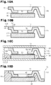
- a metal plate 100 having a predetermined thickness is first prepared.
- the metal plate 100 may have a thickness of, for example, 0.1 mm.
- a through-hole 101 is formed in the metal plate 100 by, for example, performing etching or stamping.
- the size of the through-hole 101 corresponds with the size of an inner opening 54a of the element connector 54 as shown in Fig. 1A .
- the size of the through-hole 101 is determined in accordance with the dimensions of the light emitting element 70 that is to be mounted.
- the slits 59a to 59e shown in Fig. 1A can be formed simultaneously with when the through-hole 101 is formed.
- the entire surface of the metal plate 100 is plated to form a plating layer 102.
- the metal plate 100 undergoes stamping (drawing) to form the second electrode 50 shown in Fig. 7D .
- the plating layer 102 may be formed after the stamping (drawing).
- Figs. 7A to 7D illustrate the procedures for forming a single second electrode 50
- a plurality of second electrodes 50 be simultaneously formed from the metal plate 100.
- Fig. 8A for example, multiple sets of the through-hole 101 and the slits 59a to 59e may be formed in an integral metal plate.
- stamping is performed to form a lead frame 105 including a plurality of connected second electrodes 50, each including the reflective portion 53, the element connector 54, and the terminal 55.
- a metal plate 110 with a predetermined thickness is prepared.
- the metal plate 110 may have a thickness of, for example, 0.2 mm.
- the entire surface of the metal plate 110 is plated to form a plating layer 111. This completes the first electrode 30 shown in Fig. 9B .
- an insulating sheet 40 to which an adhesive or the like has been applied, is prepared.
- the insulating sheet 40 connects the second electrode 50 to the upper surface 31 of the first electrode 30.
- the first electrode 30 is connected to the second electrode 50, which is included in the lead frame 105 shown in Fig. 8A .
- a mold tape 120 is adhered to the upper surface of the lead frame 105 (second electrode 50), which is shown in Fig. 8B .
- the mold tape 120 covers the opening 52 of the second electrode 50, or the inner side surface of the reflective portion 53, the element connector 54, and the middle area of the upper surface 31 of the first electrode 30.
- Fig. 10B illustrates the terminal 55 as if it is open in the horizontal direction (rightward in the drawing), adjacent second electrodes 50 are continuously formed in the lead frame 105 as shown in Fig. 8B .
- the mold tape 120 shown in Fig. 10B covers and closes the truncated conical recess, which is used to form the terminal 55.
- Fig. 10C the product shown in Fig. 10B including the first electrode 30 is set in a metal mold 130. Resin 140 is then injected into the metal mold 130.
- Fig. 10C illustrates the metal mold 130 accommodating a single first electrode 30 and a single second electrode 50, it is preferable that the metal mold 130 be able to accommodate the lead frame 105 shown in Fig. 8B and the first electrodes 30, which are connected to the second electrodes 50 of the lead frame 105 by the insulating sheet 40.
- the metal mold 130 is box-shaped.
- the inner height of the metal mold 130 is substantially the same as the height from the lower surface 32 of the first electrode 30 to the upper surface of the second electrode 50.
- the lower surface 32 of the first electrode 30 comes into contact with the inner surface of the metal mold 130.
- the lower surface 32 of the first electrode 30 is not covered by the resin 140.
- the frame-shaped insulating sheet 40 connects the element connector 54 of the second electrode 50 and the upper surface 31 of the first electrode 30.
- the upper surface of the second electrode 50 is covered by the mold tape 120. This prevents the resin 140 from entering the recess 11 (cavity), which is formed by the second electrode 50 and the first electrode 30, and the recess for the terminal 55.
- the resin 140 injected in the metal mold 130 is cured. Then, the molded product is removed from the metal mold 130, and the mold tape 120 is removed. A resin material is then applied to the upper surface of the second electrode 50 by, for example, performing screen printing. This forms the resist film 60. Subsequently, the lead frame 105 is cut and singulate. This forms the package 10 shown in Fig. 10D .
- the package 10 does not have to be singulated after resin molding.
- the resin molding may be performed after the singulation process.
- the lower surface 58 of the connecting terminal 57 included in the terminal 55 be substantially flush with the lower surface 21 of the housing 20.
- the side wall 56 of the terminal 55 may be covered by resin.
- a vertical cavity surface emitting laser may be used as the light emitting element.
- the light emitting element should not be limited to an element that outputs light in the visible region.
- the light emitting element may output ultraviolet rays or infrared rays.
- the light emitting element 70 and a zener diode 75 may be mounted on the package 10.
- the zener diode 75 also includes electrodes on its upper and lower surfaces for connection.
- solder or a conductive paste electrically connects the zener diode 75 to the first electrode 30, and a wire 76 electrically connects the zener diode 75 to the element connector 54.
- Fig. 11 does not show resin that covers the light emitting element 70 and the zener diode 75.
- any element other than a zener diode may be mounted on the package 10.
- a light emitting element, a protective element (e.g., zener diode or capacitor) that protects such a semiconductor element from damages caused by overvoltage, or a combination of such elements may be mounted on the package 10.
- the element connector 54 for connecting the elements is frame-shaped. This allows the mounted elements to be arranged at any position that does not affect the light emitting element 70 and allows a wire to be connected to the element connector 54.
- the shape of the first electrode 30 may be changed.
- the first electrode 30 may have a flange 33 as shown in Fig. 12 .
- the flange 33 may be formed by, for example, stamping or etching.
- the flange 33 allows for closer contact between the first electrode 30 and the resin that forms the housing 20.
- the first electrode 30 may have a lower surface 32 having a larger area than the upper surface 31.
- the first electrode 30 may be in the shape of a frustum.
Landscapes
- Led Device Packages (AREA)
Applications Claiming Priority (1)
| Application Number | Priority Date | Filing Date | Title |
|---|---|---|---|
| JP2012095488A JP5989388B2 (ja) | 2012-04-19 | 2012-04-19 | パッケージ及びパッケージの製造方法 |
Publications (3)
| Publication Number | Publication Date |
|---|---|
| EP2654093A2 EP2654093A2 (en) | 2013-10-23 |
| EP2654093A3 EP2654093A3 (en) | 2015-11-18 |
| EP2654093B1 true EP2654093B1 (en) | 2018-11-28 |
Family
ID=48326072
Family Applications (1)
| Application Number | Title | Priority Date | Filing Date |
|---|---|---|---|
| EP13163043.6A Not-in-force EP2654093B1 (en) | 2012-04-19 | 2013-04-10 | Package and method for manufacturing package |
Country Status (4)
| Country | Link |
|---|---|
| US (1) | US8890295B2 (OSRAM) |
| EP (1) | EP2654093B1 (OSRAM) |
| JP (1) | JP5989388B2 (OSRAM) |
| CN (1) | CN103378268B (OSRAM) |
Families Citing this family (15)
| Publication number | Priority date | Publication date | Assignee | Title |
|---|---|---|---|---|
| WO2014208495A1 (ja) * | 2013-06-28 | 2014-12-31 | シチズンホールディングス株式会社 | Led装置 |
| WO2015083527A1 (ja) * | 2013-12-03 | 2015-06-11 | 日本カーバイド工業株式会社 | 発光素子搭載用基板、及び、それを用いた発光装置 |
| USD778848S1 (en) * | 2015-04-07 | 2017-02-14 | Cree, Inc. | Solid state light emitter component |
| JP6168096B2 (ja) | 2015-04-28 | 2017-07-26 | 日亜化学工業株式会社 | 発光装置、パッケージ及びそれらの製造方法 |
| JP6628031B2 (ja) * | 2015-11-04 | 2020-01-08 | ローム株式会社 | 電子部品 |
| DE102016106270A1 (de) * | 2016-04-06 | 2017-10-12 | Osram Opto Semiconductors Gmbh | Herstellung eines halbleiterbauelements |
| JP1566953S (OSRAM) * | 2016-04-28 | 2017-01-16 | ||
| TWI647867B (zh) * | 2016-08-31 | 2019-01-11 | 大陸商開發晶照明(廈門)有限公司 | Led金屬基板和led模組 |
| US10378736B2 (en) * | 2016-11-03 | 2019-08-13 | Foshan Nationstar Optoelectronics Co., Ltd. | LED bracket, LED bracket array, LED device and LED display screen |
| CN108269899B (zh) * | 2016-12-30 | 2020-06-05 | 光宝光电(常州)有限公司 | 发光二极管封装结构及其制造方法 |
| WO2019059703A2 (ko) * | 2017-09-22 | 2019-03-28 | 엘지이노텍 주식회사 | 발광소자 패키지 및 조명 모듈 |
| JP6809442B2 (ja) * | 2017-11-27 | 2021-01-06 | Tdk株式会社 | センサシステム、センサモジュールおよびセンサシステムの実装方法 |
| JP7231809B2 (ja) * | 2018-06-05 | 2023-03-02 | 日亜化学工業株式会社 | 発光装置 |
| USD865688S1 (en) * | 2018-07-03 | 2019-11-05 | Lumens Co., Ltd. | LED package |
| DE112024000872T5 (de) * | 2023-05-17 | 2025-12-11 | Ams-Osram International Gmbh | Optoelektronisches halbleiterbauelement und verfahren zur herstellung eines optoelektronischen halbleiterbauelements |
Family Cites Families (14)
| Publication number | Priority date | Publication date | Assignee | Title |
|---|---|---|---|---|
| JP4066608B2 (ja) | 2001-03-16 | 2008-03-26 | 日亜化学工業株式会社 | パッケージ成形体及びその製造方法 |
| JP3912607B2 (ja) * | 2002-06-19 | 2007-05-09 | サンケン電気株式会社 | 半導体発光装置の製法 |
| JP2005197329A (ja) | 2004-01-05 | 2005-07-21 | Stanley Electric Co Ltd | 表面実装型半導体装置及びそのリードフレーム構造 |
| US20050199899A1 (en) * | 2004-03-11 | 2005-09-15 | Ming-Der Lin | Package array and package unit of flip chip LED |
| JP4571139B2 (ja) * | 2004-08-10 | 2010-10-27 | ルネサスエレクトロニクス株式会社 | 発光装置および発光装置の製造方法 |
| JP2006222271A (ja) * | 2005-02-10 | 2006-08-24 | Ngk Spark Plug Co Ltd | 発光素子実装用基板 |
| KR100735310B1 (ko) * | 2006-04-21 | 2007-07-04 | 삼성전기주식회사 | 다층 반사 면 구조를 갖는 엘이디 패키지 및 그 제조방법 |
| TWI314366B (en) * | 2006-04-28 | 2009-09-01 | Delta Electronics Inc | Light emitting apparatus |
| US7485480B2 (en) * | 2006-09-21 | 2009-02-03 | Harvatek Corporation | Method of manufacturing high power light-emitting device package and structure thereof |
| US20080089072A1 (en) * | 2006-10-11 | 2008-04-17 | Alti-Electronics Co., Ltd. | High Power Light Emitting Diode Package |
| US8058667B2 (en) * | 2009-03-10 | 2011-11-15 | Nepes Led Corporation | Leadframe package for light emitting diode device |
| WO2010119830A1 (ja) * | 2009-04-13 | 2010-10-21 | パナソニック電工株式会社 | 発光ダイオード |
| DE102010025319B4 (de) * | 2010-06-28 | 2022-05-25 | OSRAM Opto Semiconductors Gesellschaft mit beschränkter Haftung | Verfahren zur Herstellung eines oberflächenmontierbaren Halbleiterbauelements und oberflächenmontierbare Halbleiterbauelemente |
| US8253330B2 (en) * | 2010-11-30 | 2012-08-28 | GEM Weltronics TWN Corporation | Airtight multi-layer array type LED |
-
2012
- 2012-04-19 JP JP2012095488A patent/JP5989388B2/ja not_active Expired - Fee Related
-
2013
- 2013-04-10 EP EP13163043.6A patent/EP2654093B1/en not_active Not-in-force
- 2013-04-16 CN CN201310131498.0A patent/CN103378268B/zh not_active Expired - Fee Related
- 2013-04-17 US US13/864,402 patent/US8890295B2/en not_active Expired - Fee Related
Non-Patent Citations (1)
| Title |
|---|
| None * |
Also Published As
| Publication number | Publication date |
|---|---|
| JP2013222931A (ja) | 2013-10-28 |
| EP2654093A3 (en) | 2015-11-18 |
| CN103378268B (zh) | 2017-10-03 |
| US8890295B2 (en) | 2014-11-18 |
| JP5989388B2 (ja) | 2016-09-07 |
| EP2654093A2 (en) | 2013-10-23 |
| US20130277701A1 (en) | 2013-10-24 |
| CN103378268A (zh) | 2013-10-30 |
Similar Documents
| Publication | Publication Date | Title |
|---|---|---|
| EP2654093B1 (en) | Package and method for manufacturing package | |
| US11211536B2 (en) | Semiconductor device package and a method of manufacturing the same | |
| US9512968B2 (en) | LED module | |
| EP1998380A2 (en) | Semiconductor light-emitting device | |
| US10667345B2 (en) | Method for manufacturing light-emitting device packages, light-emitting device package strip, and light-emitting device package | |
| KR101149645B1 (ko) | 광커플러 장치들 | |
| EP2215667A2 (en) | Led package and method for fabricating the same | |
| US9735320B2 (en) | LED packages and manufacturing method thereof | |
| US20100213484A1 (en) | Lead frame assembly, package structure and LED package structure | |
| JP6753051B2 (ja) | 発光装置 | |
| US11223000B2 (en) | Method of manufacturing light emitting element mounting base member, method of manufacturing light emitting device using the light emitting element mounting base member, light emitting element mounting base member, and light emitting device using the light emitting element mounting base member | |
| US11315913B2 (en) | Light emitting device and method of manufacturing the light emitting device | |
| KR20170045544A (ko) | 발광 다이오드 패키지 및 그의 제조 방법 | |
| KR101273045B1 (ko) | 발광 다이오드 패키지 | |
| JP7011148B2 (ja) | 発光素子載置用基体の製造方法及びそれを用いた発光装置の製造方法並びに発光素子載置用基体及びそれを用いた発光装置 | |
| TWI521745B (zh) | 發光二極體封裝結構及其製造方法 | |
| JP2012212738A (ja) | 光半導体装置 | |
| JP2013115343A (ja) | 樹脂成形フレーム及び光半導体装置 | |
| HK1120334A (en) | Semiconductor light-emitting device |
Legal Events
| Date | Code | Title | Description |
|---|---|---|---|
| PUAI | Public reference made under article 153(3) epc to a published international application that has entered the european phase |
Free format text: ORIGINAL CODE: 0009012 |
|
| AK | Designated contracting states |
Kind code of ref document: A2 Designated state(s): AL AT BE BG CH CY CZ DE DK EE ES FI FR GB GR HR HU IE IS IT LI LT LU LV MC MK MT NL NO PL PT RO RS SE SI SK SM TR |
|
| AX | Request for extension of the european patent |
Extension state: BA ME |
|
| PUAL | Search report despatched |
Free format text: ORIGINAL CODE: 0009013 |
|
| AK | Designated contracting states |
Kind code of ref document: A3 Designated state(s): AL AT BE BG CH CY CZ DE DK EE ES FI FR GB GR HR HU IE IS IT LI LT LU LV MC MK MT NL NO PL PT RO RS SE SI SK SM TR |
|
| AX | Request for extension of the european patent |
Extension state: BA ME |
|
| RIC1 | Information provided on ipc code assigned before grant |
Ipc: H01L 33/62 20100101ALN20151009BHEP Ipc: H01L 33/00 20100101ALN20151009BHEP Ipc: H01L 33/48 20100101ALN20151009BHEP Ipc: H01L 33/64 20100101AFI20151009BHEP |
|
| 17P | Request for examination filed |
Effective date: 20160516 |
|
| RBV | Designated contracting states (corrected) |
Designated state(s): AL AT BE BG CH CY CZ DE DK EE ES FI FR GB GR HR HU IE IS IT LI LT LU LV MC MK MT NL NO PL PT RO RS SE SI SK SM TR |
|
| RIC1 | Information provided on ipc code assigned before grant |
Ipc: H01L 33/62 20100101ALI20180328BHEP Ipc: H01L 33/64 20100101AFI20180328BHEP Ipc: H01L 33/00 20100101ALN20180328BHEP Ipc: H01L 33/48 20100101ALN20180328BHEP |
|
| GRAP | Despatch of communication of intention to grant a patent |
Free format text: ORIGINAL CODE: EPIDOSNIGR1 |
|
| STAA | Information on the status of an ep patent application or granted ep patent |
Free format text: STATUS: GRANT OF PATENT IS INTENDED |
|
| INTG | Intention to grant announced |
Effective date: 20180507 |
|
| GRAJ | Information related to disapproval of communication of intention to grant by the applicant or resumption of examination proceedings by the epo deleted |
Free format text: ORIGINAL CODE: EPIDOSDIGR1 |
|
| STAA | Information on the status of an ep patent application or granted ep patent |
Free format text: STATUS: REQUEST FOR EXAMINATION WAS MADE |
|
| GRAS | Grant fee paid |
Free format text: ORIGINAL CODE: EPIDOSNIGR3 |
|
| STAA | Information on the status of an ep patent application or granted ep patent |
Free format text: STATUS: GRANT OF PATENT IS INTENDED |
|
| GRAP | Despatch of communication of intention to grant a patent |
Free format text: ORIGINAL CODE: EPIDOSNIGR1 |
|
| INTC | Intention to grant announced (deleted) | ||
| INTG | Intention to grant announced |
Effective date: 20180907 |
|
| RIC1 | Information provided on ipc code assigned before grant |
Ipc: H01L 33/64 20100101AFI20180827BHEP Ipc: H01L 33/48 20100101ALN20180827BHEP Ipc: H01L 33/62 20100101ALI20180827BHEP Ipc: H01L 33/00 20100101ALN20180827BHEP |
|
| GRAA | (expected) grant |
Free format text: ORIGINAL CODE: 0009210 |
|
| STAA | Information on the status of an ep patent application or granted ep patent |
Free format text: STATUS: THE PATENT HAS BEEN GRANTED |
|
| AK | Designated contracting states |
Kind code of ref document: B1 Designated state(s): AL AT BE BG CH CY CZ DE DK EE ES FI FR GB GR HR HU IE IS IT LI LT LU LV MC MK MT NL NO PL PT RO RS SE SI SK SM TR |
|
| REG | Reference to a national code |
Ref country code: GB Ref legal event code: FG4D |
|
| REG | Reference to a national code |
Ref country code: CH Ref legal event code: EP |
|
| REG | Reference to a national code |
Ref country code: AT Ref legal event code: REF Ref document number: 1071253 Country of ref document: AT Kind code of ref document: T Effective date: 20181215 |
|
| REG | Reference to a national code |
Ref country code: DE Ref legal event code: R096 Ref document number: 602013047354 Country of ref document: DE |
|
| REG | Reference to a national code |
Ref country code: IE Ref legal event code: FG4D |
|
| REG | Reference to a national code |
Ref country code: NL Ref legal event code: MP Effective date: 20181128 |
|
| REG | Reference to a national code |
Ref country code: LT Ref legal event code: MG4D |
|
| REG | Reference to a national code |
Ref country code: AT Ref legal event code: MK05 Ref document number: 1071253 Country of ref document: AT Kind code of ref document: T Effective date: 20181128 |
|
| PG25 | Lapsed in a contracting state [announced via postgrant information from national office to epo] |
Ref country code: LV Free format text: LAPSE BECAUSE OF FAILURE TO SUBMIT A TRANSLATION OF THE DESCRIPTION OR TO PAY THE FEE WITHIN THE PRESCRIBED TIME-LIMIT Effective date: 20181128 Ref country code: AT Free format text: LAPSE BECAUSE OF FAILURE TO SUBMIT A TRANSLATION OF THE DESCRIPTION OR TO PAY THE FEE WITHIN THE PRESCRIBED TIME-LIMIT Effective date: 20181128 Ref country code: ES Free format text: LAPSE BECAUSE OF FAILURE TO SUBMIT A TRANSLATION OF THE DESCRIPTION OR TO PAY THE FEE WITHIN THE PRESCRIBED TIME-LIMIT Effective date: 20181128 Ref country code: NO Free format text: LAPSE BECAUSE OF FAILURE TO SUBMIT A TRANSLATION OF THE DESCRIPTION OR TO PAY THE FEE WITHIN THE PRESCRIBED TIME-LIMIT Effective date: 20190228 Ref country code: IS Free format text: LAPSE BECAUSE OF FAILURE TO SUBMIT A TRANSLATION OF THE DESCRIPTION OR TO PAY THE FEE WITHIN THE PRESCRIBED TIME-LIMIT Effective date: 20190328 Ref country code: FI Free format text: LAPSE BECAUSE OF FAILURE TO SUBMIT A TRANSLATION OF THE DESCRIPTION OR TO PAY THE FEE WITHIN THE PRESCRIBED TIME-LIMIT Effective date: 20181128 Ref country code: BG Free format text: LAPSE BECAUSE OF FAILURE TO SUBMIT A TRANSLATION OF THE DESCRIPTION OR TO PAY THE FEE WITHIN THE PRESCRIBED TIME-LIMIT Effective date: 20190228 Ref country code: LT Free format text: LAPSE BECAUSE OF FAILURE TO SUBMIT A TRANSLATION OF THE DESCRIPTION OR TO PAY THE FEE WITHIN THE PRESCRIBED TIME-LIMIT Effective date: 20181128 Ref country code: HR Free format text: LAPSE BECAUSE OF FAILURE TO SUBMIT A TRANSLATION OF THE DESCRIPTION OR TO PAY THE FEE WITHIN THE PRESCRIBED TIME-LIMIT Effective date: 20181128 |
|
| PG25 | Lapsed in a contracting state [announced via postgrant information from national office to epo] |
Ref country code: SE Free format text: LAPSE BECAUSE OF FAILURE TO SUBMIT A TRANSLATION OF THE DESCRIPTION OR TO PAY THE FEE WITHIN THE PRESCRIBED TIME-LIMIT Effective date: 20181128 Ref country code: AL Free format text: LAPSE BECAUSE OF FAILURE TO SUBMIT A TRANSLATION OF THE DESCRIPTION OR TO PAY THE FEE WITHIN THE PRESCRIBED TIME-LIMIT Effective date: 20181128 Ref country code: PT Free format text: LAPSE BECAUSE OF FAILURE TO SUBMIT A TRANSLATION OF THE DESCRIPTION OR TO PAY THE FEE WITHIN THE PRESCRIBED TIME-LIMIT Effective date: 20190328 Ref country code: RS Free format text: LAPSE BECAUSE OF FAILURE TO SUBMIT A TRANSLATION OF THE DESCRIPTION OR TO PAY THE FEE WITHIN THE PRESCRIBED TIME-LIMIT Effective date: 20181128 Ref country code: GR Free format text: LAPSE BECAUSE OF FAILURE TO SUBMIT A TRANSLATION OF THE DESCRIPTION OR TO PAY THE FEE WITHIN THE PRESCRIBED TIME-LIMIT Effective date: 20190301 |
|
| PG25 | Lapsed in a contracting state [announced via postgrant information from national office to epo] |
Ref country code: NL Free format text: LAPSE BECAUSE OF FAILURE TO SUBMIT A TRANSLATION OF THE DESCRIPTION OR TO PAY THE FEE WITHIN THE PRESCRIBED TIME-LIMIT Effective date: 20181128 |
|
| PG25 | Lapsed in a contracting state [announced via postgrant information from national office to epo] |
Ref country code: DK Free format text: LAPSE BECAUSE OF FAILURE TO SUBMIT A TRANSLATION OF THE DESCRIPTION OR TO PAY THE FEE WITHIN THE PRESCRIBED TIME-LIMIT Effective date: 20181128 Ref country code: PL Free format text: LAPSE BECAUSE OF FAILURE TO SUBMIT A TRANSLATION OF THE DESCRIPTION OR TO PAY THE FEE WITHIN THE PRESCRIBED TIME-LIMIT Effective date: 20181128 Ref country code: CZ Free format text: LAPSE BECAUSE OF FAILURE TO SUBMIT A TRANSLATION OF THE DESCRIPTION OR TO PAY THE FEE WITHIN THE PRESCRIBED TIME-LIMIT Effective date: 20181128 Ref country code: IT Free format text: LAPSE BECAUSE OF FAILURE TO SUBMIT A TRANSLATION OF THE DESCRIPTION OR TO PAY THE FEE WITHIN THE PRESCRIBED TIME-LIMIT Effective date: 20181128 |
|
| REG | Reference to a national code |
Ref country code: DE Ref legal event code: R097 Ref document number: 602013047354 Country of ref document: DE |
|
| PG25 | Lapsed in a contracting state [announced via postgrant information from national office to epo] |
Ref country code: RO Free format text: LAPSE BECAUSE OF FAILURE TO SUBMIT A TRANSLATION OF THE DESCRIPTION OR TO PAY THE FEE WITHIN THE PRESCRIBED TIME-LIMIT Effective date: 20181128 Ref country code: SM Free format text: LAPSE BECAUSE OF FAILURE TO SUBMIT A TRANSLATION OF THE DESCRIPTION OR TO PAY THE FEE WITHIN THE PRESCRIBED TIME-LIMIT Effective date: 20181128 Ref country code: EE Free format text: LAPSE BECAUSE OF FAILURE TO SUBMIT A TRANSLATION OF THE DESCRIPTION OR TO PAY THE FEE WITHIN THE PRESCRIBED TIME-LIMIT Effective date: 20181128 Ref country code: SK Free format text: LAPSE BECAUSE OF FAILURE TO SUBMIT A TRANSLATION OF THE DESCRIPTION OR TO PAY THE FEE WITHIN THE PRESCRIBED TIME-LIMIT Effective date: 20181128 |
|
| PLBE | No opposition filed within time limit |
Free format text: ORIGINAL CODE: 0009261 |
|
| STAA | Information on the status of an ep patent application or granted ep patent |
Free format text: STATUS: NO OPPOSITION FILED WITHIN TIME LIMIT |
|
| PG25 | Lapsed in a contracting state [announced via postgrant information from national office to epo] |
Ref country code: SI Free format text: LAPSE BECAUSE OF FAILURE TO SUBMIT A TRANSLATION OF THE DESCRIPTION OR TO PAY THE FEE WITHIN THE PRESCRIBED TIME-LIMIT Effective date: 20181128 |
|
| 26N | No opposition filed |
Effective date: 20190829 |
|
| REG | Reference to a national code |
Ref country code: CH Ref legal event code: PL |
|
| REG | Reference to a national code |
Ref country code: BE Ref legal event code: MM Effective date: 20190430 |
|
| GBPC | Gb: european patent ceased through non-payment of renewal fee |
Effective date: 20190410 |
|
| PG25 | Lapsed in a contracting state [announced via postgrant information from national office to epo] |
Ref country code: MC Free format text: LAPSE BECAUSE OF FAILURE TO SUBMIT A TRANSLATION OF THE DESCRIPTION OR TO PAY THE FEE WITHIN THE PRESCRIBED TIME-LIMIT Effective date: 20181128 Ref country code: LU Free format text: LAPSE BECAUSE OF NON-PAYMENT OF DUE FEES Effective date: 20190410 |
|
| PG25 | Lapsed in a contracting state [announced via postgrant information from national office to epo] |
Ref country code: CH Free format text: LAPSE BECAUSE OF NON-PAYMENT OF DUE FEES Effective date: 20190430 Ref country code: GB Free format text: LAPSE BECAUSE OF NON-PAYMENT OF DUE FEES Effective date: 20190410 Ref country code: LI Free format text: LAPSE BECAUSE OF NON-PAYMENT OF DUE FEES Effective date: 20190430 |
|
| PG25 | Lapsed in a contracting state [announced via postgrant information from national office to epo] |
Ref country code: BE Free format text: LAPSE BECAUSE OF NON-PAYMENT OF DUE FEES Effective date: 20190430 |
|
| PG25 | Lapsed in a contracting state [announced via postgrant information from national office to epo] |
Ref country code: TR Free format text: LAPSE BECAUSE OF FAILURE TO SUBMIT A TRANSLATION OF THE DESCRIPTION OR TO PAY THE FEE WITHIN THE PRESCRIBED TIME-LIMIT Effective date: 20181128 |
|
| PG25 | Lapsed in a contracting state [announced via postgrant information from national office to epo] |
Ref country code: IE Free format text: LAPSE BECAUSE OF NON-PAYMENT OF DUE FEES Effective date: 20190410 |
|
| PG25 | Lapsed in a contracting state [announced via postgrant information from national office to epo] |
Ref country code: FR Free format text: LAPSE BECAUSE OF NON-PAYMENT OF DUE FEES Effective date: 20190430 |
|
| PG25 | Lapsed in a contracting state [announced via postgrant information from national office to epo] |
Ref country code: CY Free format text: LAPSE BECAUSE OF FAILURE TO SUBMIT A TRANSLATION OF THE DESCRIPTION OR TO PAY THE FEE WITHIN THE PRESCRIBED TIME-LIMIT Effective date: 20181128 |
|
| PG25 | Lapsed in a contracting state [announced via postgrant information from national office to epo] |
Ref country code: HU Free format text: LAPSE BECAUSE OF FAILURE TO SUBMIT A TRANSLATION OF THE DESCRIPTION OR TO PAY THE FEE WITHIN THE PRESCRIBED TIME-LIMIT; INVALID AB INITIO Effective date: 20130410 Ref country code: MT Free format text: LAPSE BECAUSE OF FAILURE TO SUBMIT A TRANSLATION OF THE DESCRIPTION OR TO PAY THE FEE WITHIN THE PRESCRIBED TIME-LIMIT Effective date: 20181128 |
|
| PGFP | Annual fee paid to national office [announced via postgrant information from national office to epo] |
Ref country code: DE Payment date: 20210316 Year of fee payment: 9 |
|
| PG25 | Lapsed in a contracting state [announced via postgrant information from national office to epo] |
Ref country code: MK Free format text: LAPSE BECAUSE OF FAILURE TO SUBMIT A TRANSLATION OF THE DESCRIPTION OR TO PAY THE FEE WITHIN THE PRESCRIBED TIME-LIMIT Effective date: 20181128 |
|
| REG | Reference to a national code |
Ref country code: DE Ref legal event code: R119 Ref document number: 602013047354 Country of ref document: DE |
|
| PG25 | Lapsed in a contracting state [announced via postgrant information from national office to epo] |
Ref country code: DE Free format text: LAPSE BECAUSE OF NON-PAYMENT OF DUE FEES Effective date: 20221103 |