EP2653014B1 - Passage d'un mode de conduction discontinu au mode de conduction critique basé sur un paramètre de commutation - Google Patents
Passage d'un mode de conduction discontinu au mode de conduction critique basé sur un paramètre de commutation Download PDFInfo
- Publication number
- EP2653014B1 EP2653014B1 EP11813481.6A EP11813481A EP2653014B1 EP 2653014 B1 EP2653014 B1 EP 2653014B1 EP 11813481 A EP11813481 A EP 11813481A EP 2653014 B1 EP2653014 B1 EP 2653014B1
- Authority
- EP
- European Patent Office
- Prior art keywords
- time
- power converter
- switching power
- switch
- conduction mode
- Prior art date
- Legal status (The legal status is an assumption and is not a legal conclusion. Google has not performed a legal analysis and makes no representation as to the accuracy of the status listed.)
- Active
Links
- 230000007704 transition Effects 0.000 title claims description 75
- 238000000034 method Methods 0.000 claims description 16
- 238000006243 chemical reaction Methods 0.000 claims description 3
- 230000000737 periodic effect Effects 0.000 claims 1
- 230000007423 decrease Effects 0.000 description 13
- 230000001276 controlling effect Effects 0.000 description 8
- 230000001105 regulatory effect Effects 0.000 description 5
- 239000003990 capacitor Substances 0.000 description 4
- 230000003071 parasitic effect Effects 0.000 description 4
- 238000004804 winding Methods 0.000 description 4
- 230000009977 dual effect Effects 0.000 description 3
- 230000000694 effects Effects 0.000 description 3
- 230000008901 benefit Effects 0.000 description 2
- 230000008859 change Effects 0.000 description 2
- 239000002131 composite material Substances 0.000 description 2
- 230000003247 decreasing effect Effects 0.000 description 2
- 230000005669 field effect Effects 0.000 description 2
- 230000006870 function Effects 0.000 description 2
- 230000008569 process Effects 0.000 description 2
- 239000013643 reference control Substances 0.000 description 2
- 239000008186 active pharmaceutical agent Substances 0.000 description 1
- 230000004075 alteration Effects 0.000 description 1
- 238000001514 detection method Methods 0.000 description 1
- 238000007599 discharging Methods 0.000 description 1
- 238000006467 substitution reaction Methods 0.000 description 1
Images


Classifications
-
- H—ELECTRICITY
- H05—ELECTRIC TECHNIQUES NOT OTHERWISE PROVIDED FOR
- H05B—ELECTRIC HEATING; ELECTRIC LIGHT SOURCES NOT OTHERWISE PROVIDED FOR; CIRCUIT ARRANGEMENTS FOR ELECTRIC LIGHT SOURCES, IN GENERAL
- H05B45/00—Circuit arrangements for operating light-emitting diodes [LED]
- H05B45/30—Driver circuits
- H05B45/37—Converter circuits
- H05B45/3725—Switched mode power supply [SMPS]
- H05B45/385—Switched mode power supply [SMPS] using flyback topology
-
- H—ELECTRICITY
- H02—GENERATION; CONVERSION OR DISTRIBUTION OF ELECTRIC POWER
- H02M—APPARATUS FOR CONVERSION BETWEEN AC AND AC, BETWEEN AC AND DC, OR BETWEEN DC AND DC, AND FOR USE WITH MAINS OR SIMILAR POWER SUPPLY SYSTEMS; CONVERSION OF DC OR AC INPUT POWER INTO SURGE OUTPUT POWER; CONTROL OR REGULATION THEREOF
- H02M3/00—Conversion of dc power input into dc power output
- H02M3/22—Conversion of dc power input into dc power output with intermediate conversion into ac
- H02M3/24—Conversion of dc power input into dc power output with intermediate conversion into ac by static converters
- H02M3/28—Conversion of dc power input into dc power output with intermediate conversion into ac by static converters using discharge tubes with control electrode or semiconductor devices with control electrode to produce the intermediate ac
- H02M3/325—Conversion of dc power input into dc power output with intermediate conversion into ac by static converters using discharge tubes with control electrode or semiconductor devices with control electrode to produce the intermediate ac using devices of a triode or a transistor type requiring continuous application of a control signal
- H02M3/335—Conversion of dc power input into dc power output with intermediate conversion into ac by static converters using discharge tubes with control electrode or semiconductor devices with control electrode to produce the intermediate ac using devices of a triode or a transistor type requiring continuous application of a control signal using semiconductor devices only
- H02M3/33507—Conversion of dc power input into dc power output with intermediate conversion into ac by static converters using discharge tubes with control electrode or semiconductor devices with control electrode to produce the intermediate ac using devices of a triode or a transistor type requiring continuous application of a control signal using semiconductor devices only with automatic control of the output voltage or current, e.g. flyback converters
- H02M3/33523—Conversion of dc power input into dc power output with intermediate conversion into ac by static converters using discharge tubes with control electrode or semiconductor devices with control electrode to produce the intermediate ac using devices of a triode or a transistor type requiring continuous application of a control signal using semiconductor devices only with automatic control of the output voltage or current, e.g. flyback converters with galvanic isolation between input and output of both the power stage and the feedback loop
-
- H—ELECTRICITY
- H02—GENERATION; CONVERSION OR DISTRIBUTION OF ELECTRIC POWER
- H02M—APPARATUS FOR CONVERSION BETWEEN AC AND AC, BETWEEN AC AND DC, OR BETWEEN DC AND DC, AND FOR USE WITH MAINS OR SIMILAR POWER SUPPLY SYSTEMS; CONVERSION OF DC OR AC INPUT POWER INTO SURGE OUTPUT POWER; CONTROL OR REGULATION THEREOF
- H02M1/00—Details of apparatus for conversion
- H02M1/0003—Details of control, feedback or regulation circuits
-
- H—ELECTRICITY
- H02—GENERATION; CONVERSION OR DISTRIBUTION OF ELECTRIC POWER
- H02M—APPARATUS FOR CONVERSION BETWEEN AC AND AC, BETWEEN AC AND DC, OR BETWEEN DC AND DC, AND FOR USE WITH MAINS OR SIMILAR POWER SUPPLY SYSTEMS; CONVERSION OF DC OR AC INPUT POWER INTO SURGE OUTPUT POWER; CONTROL OR REGULATION THEREOF
- H02M1/00—Details of apparatus for conversion
- H02M1/0067—Converter structures employing plural converter units, other than for parallel operation of the units on a single load
- H02M1/007—Plural converter units in cascade
-
- H—ELECTRICITY
- H05—ELECTRIC TECHNIQUES NOT OTHERWISE PROVIDED FOR
- H05B—ELECTRIC HEATING; ELECTRIC LIGHT SOURCES NOT OTHERWISE PROVIDED FOR; CIRCUIT ARRANGEMENTS FOR ELECTRIC LIGHT SOURCES, IN GENERAL
- H05B45/00—Circuit arrangements for operating light-emitting diodes [LED]
- H05B45/30—Driver circuits
- H05B45/37—Converter circuits
- H05B45/3725—Switched mode power supply [SMPS]
-
- Y—GENERAL TAGGING OF NEW TECHNOLOGICAL DEVELOPMENTS; GENERAL TAGGING OF CROSS-SECTIONAL TECHNOLOGIES SPANNING OVER SEVERAL SECTIONS OF THE IPC; TECHNICAL SUBJECTS COVERED BY FORMER USPC CROSS-REFERENCE ART COLLECTIONS [XRACs] AND DIGESTS
- Y02—TECHNOLOGIES OR APPLICATIONS FOR MITIGATION OR ADAPTATION AGAINST CLIMATE CHANGE
- Y02B—CLIMATE CHANGE MITIGATION TECHNOLOGIES RELATED TO BUILDINGS, e.g. HOUSING, HOUSE APPLIANCES OR RELATED END-USER APPLICATIONS
- Y02B20/00—Energy efficient lighting technologies, e.g. halogen lamps or gas discharge lamps
- Y02B20/30—Semiconductor lamps, e.g. solid state lamps [SSL] light emitting diodes [LED] or organic LED [OLED]
Definitions
- the present invention relates in general to the field of electronics, and more specifically to a method and system for determining and utilizing a switching parameter of a switching power converter to facilitate transitions between discontinuous conduction mode and critical conduction mode.
- switching power converters to provide efficient power conversion from a voltage supply into a regulated output voltage.
- switching power converters When converting an alternating current ("AC") supply voltage into a regulated output voltage, switching power converters utilize a switch that turns ON and OFF multiple times during a single cycle of the AC supply voltage. The ratio of the ON time of the switch to the OFF time correlates to an average power conversion. Improving the energy efficiency of electrical circuits, including switching power converters, continues to be a high priority for many entities including many companies and countries.
- Switching power converters generally operate in one of three different modes: discontinuous conduction mode (“DCM”), critical conduction mode (“CRM”), and continuous conduction mode (“CCM”).
- DCM discontinuous conduction mode
- CCM critical conduction mode
- CCM continuous conduction mode
- a rectified AC supply voltage rises from zero volts (0V) to a peak voltage, returns to 0V, and repeats.
- the switch in the switching power converter cycles many times during a single cycle of the rectified AC supply voltage. For example, the switching frequency of the switch is often between 20 kHz and 100kHz while the frequency of a rectified AC supply voltage is generally between 100Hz and 120Hz.
- DCM tends to be more efficient than CRM during the lower voltages of a cycle of the rectified AC supply voltage.
- CRM tends to be more efficient than DCM at higher voltages of the rectified AC supply voltage cycle.
- FIG. 1 depicts an electronic system 100 that operates in dual conduction mode to take advantage of DCM efficiencies at lower supply voltages and CRM at higher supply voltages.
- the electronic system 100 receives an AC supply voltage V SUPPLY from voltage supply 102.
- the supply voltage V IN is, for example, a nominally 60 Hz/110 V line voltage in the United States of America or a nominally 50 Hz/220 V line voltage in Europe and the People's Republic of China.
- An optional dimmer 104 phase cuts leading and/or trailing edges of the supply voltage V SUPPLY .
- the input voltage V IN represents the supply voltage V SUPPLY in the absence of phase cutting by the dimmer 104 and represents a phase cut voltage if dimmer 104 phase cuts the supply voltage V SUPPLY .
- a full-bridge diode rectifier 106 rectifies the input voltage V IN and an electromagnetic interference (EMI) filter 108 attenuates high frequency interference of the switching power converter 112 to generate a rectified input voltage V X .
- the controller 111 generates a switch control signal CS 1 to control the switching power converter 112.
- the control signal CS 1 controls the conductivity of field effect transistor (FET) switch 114 to control the primary current i P to meet the power demands of load 116.
- FET field effect transistor
- the FET conducts (i.e. ON) when during a pulse of the switch control signal CS 1 and is nonconductive (i.e. OFF) when the pulse of the switch control signal CS 1 ends.
- FIG. 2 depicts waveforms 200 associated with a switching power converter 112.
- the primary current i P ramps up through the primary coil 118 of transformer 120.
- the dot convention of transformer 120 and the diode 122 prevent flow of the secondary current is during the period T1.
- the controller 111 When the controller 111 generates the switch control signal CS 1 to turn FET 114 OFF and period T1 thereby ends, the primary current i P falls to 0, and the voltage across the primary coil 118 reverses (also referred to as "flyback").
- the flyback period T2 the secondary current is quickly rises and then decays.
- the flyback period T2 ends when the secondary current is reaches zero.
- the controller 111 waits for an idle period T3 before beginning a new period TT of the switch control signal CS 1 with a pulse of switch control signal CS 1 .
- the controller 11 begins a new period TT of the switch control signal and the primary current i P again ramps up until the end of the period T1.
- the primary charging period T1 equals the duration of the pulse of the switch control signal CS 1 . Since the controller 111 controls the duration of the pulse of the switch control signal CS 1 , the controller 111 controls the duration of the charging period T1.
- the duration of the flyback period T2 is a function of several variables such as parasitic resistances on the secondary side of the transformer 120, such as parasitic resistances of the secondary coil 124, diode 122, capacitor 126, and the secondary current is drawn by the load 116.
- FIG. 3 depicts exemplary waveforms 300 associated with the electronic system 100 for two cycles of the rectified input voltage V X , i.e. for two half-line cycles of the supply voltage V SUPPLY .
- the waveforms 300 includes superimposed waveforms for the rectified input voltage V X , a representative primary current i P , and representative secondary current is.
- the waveforms 300 also include a representative depiction of the switch control signal CS 1 .
- the term "representative" is used because typically the frequency of the switch control signal CS 1 is 20 kHz to 100 kHz and the frequency of the rectified input voltage V X is 100 Hz to 120 Hz. Thus, for clarity only a subset of the pulses of the switch control signal CS 1 and resulting primary current i P and secondary current is waveforms are shown in the waveforms 300.
- the controller 111 controls the switching power converter 112 to provide power factor correction in addition to regulating the primary side current i P .
- the controller 111 attempts to make the circuit appear resistive to the voltage supply 102 and, thus, create a linear relationship between the primary current i P and the rectified input voltage V X .
- the controller 111 generates a pulse of the switch control signal CS 1 .
- the controller 111 monitors the rectified input voltage V X via feedforward path 128, and the primary current i P rises during the charging period T1 in correlation with a near instantaneous value of the rectified input voltage V X .
- the controller 111 also monitors the secondary current is and, thus, the flyback period T2 via feedback path 130 to determine the power demand of load 116 and to regulate the secondary current is in accordance with the power demand of load 116.
- the charging period T1 and the flyback period T2 are shorter nearer to the zero crossings of the rectified input voltage V X .
- Zero crossings of the rectified input voltage V X occur in Figure 3 at times to, t 1 , and t 2 .
- the period TT of the switch control signal CS 1 during CRM is T1+T2
- the switching frequency 1/TT of the FET 114 would be highest for lower values of the rectified input voltage V X . Higher switching frequencies can correspond to higher switching losses and, thus, lower efficiency.
- the frequency of the switch control signal CS 1 during DCM is 1/(T1+T2+T3).
- Adding the idle time T3 to the period TT of the switch control signal CS 1 decreases the frequency and, thus, increases the efficiency of the FET 114 during DCM.
- the flyback period T2 increases.
- the frequency of the switch control signal CS 1 decreases while transferring more energy to the load 116. Since CRM is more efficient at higher voltages, the controller 111 generates the switch control signal CS 1 to operate the switching power converter 112 in CRM at higher values of the rectified input voltage V X .
- the instantaneous pulses of the primary current i P result in an average primary current i P_AVG that is intended to linearly track the rectified input voltage Vx.
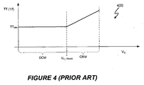
- Figure 4 depicts a period versus voltage graph 400 that represents DCM and CRM periods TT of switch control signal CS 1 relative to the rectified input voltage V X .
- the controller 111 includes a DCM/CRM fixed minimum period TT module 132 to determine when to transition between DCM and CRM operation of switching power converter 112.
- the DCM/CRM fixed minimum period TT module 132 is configured to always enforce a fixed minimum period TT MIN by generating a DCM/CRM transition signal, which controls whether the controller 111 operates the switching power converter 112 in DCM or CRM.
- the minimum TT MIN determines a transition point between DCM and CRM operation at V X_TRANS .
- the controller 111 operates the switching power converter 112 in CRM as long as the period TT is greater than the fixed minimum period TT MIN and otherwise operates the switching power converter 112 in DCM.
- the fixed minimum period TT MIN is unresponsive to changes in operating parameters of the electronic system 100 but is relatively simple to enforce since the controller 111 determines the charging period T1 and the DCM/CRM fixed minimum period TT module 132 monitors the flyback period T2 via feedback path 130.
- US 2010 002480 describes a fly back converter with a switch control coupled to an inductor switch controlling current through a primary inductor of the converter by adjusting the switch on time for constant output current in constant current mode and constant output voltage in constant voltage mode.
- the converter transitions from critical conduction mode to discontinuous conduction mode at light loads.
- US 2008 205103 describes a converter with an inductance via which current is supplied to a load.
- a switch controls the current and is switched at a first frequency for a continuous mode and a second frequency for a discontinuous mode.
- US 7,733,678 describes power factor correction in mixed operation modes.
- the duty and frequency of a boost switch is computed and the operation mode of the converter is switched between continuous, critical and discontinuous mode according to input voltage or the load.
- EP 2 144 356 describes detection of a threshold for entering and leaving a discontinuous current mode of a converter. In order to expedite the transition from DCM mode to CCM mode the time delay between two or more pulses of a current through an inductor is monitored and compared to a defined threshold.
- an apparatus comprising: a controller to provide at least dual-mode conduction control of a switching power converter, wherein the controller is capable to: control transitions between discontinuous conduction mode and critical conduction mode of the switching power converter using a measured switching time duration parameter having a value corresponding with an approximately peak voltage of a time-varying rectified input voltage supplied to the switching power converter.
- a corresponding method is also provided according to claim 4.
- an apparatus in at least one embodiment of the present invention, includes a controller to provide at least dual-mode conduction control of a switching power converter.
- the controller is capable of controlling transitions between discontinuous conduction mode and critical conduction mode of the switching power converter using a measured switching time parameter having a value corresponding with an approximately peak voltage of a time-varying supply voltage supplied to the switching power converter.
- a method in another embodiment, includes providing at least dual-mode conduction control of a switching power converter.
- Providing at least dual-mode conduction control of a switching power converter includes controlling transitions between discontinuous conduction mode and critical conduction mode of the switching power converter using a measured switching time parameter having a value corresponding with an approximately peak voltage of a time-varying supply voltage supplied to the switching power converter.
- an apparatus in a further embodiment of the present invention, includes a switching power converter.
- the apparatus further includes a controller, coupled to the switching power converter, to provide at least dual-mode conduction control of the switching power converter.
- the controller is capable of controlling transitions between discontinuous conduction mode and critical conduction mode of the switching power converter using a measured switching time parameter having a value corresponding with an approximately peak voltage of a time-varying supply voltage supplied to the switching power converter.
- the controller is further capable of controlling power factor correction for the switching power converter.
- the apparatus also includes a load coupled to the switching power converter.
- an electronic system includes a controller to provide at least dual-mode conduction control of a switching power converter.
- "At least dual-mode conduction control” means, in at least one embodiment, providing control for at least two modes of conduction such as two or more of discontinuous conduction mode (DCM), critical conduction mode (CRM), and continuous conduction mode (CCM).
- the controller is capable to control transitions between DCM and CRM of the switching power converter using a measured switching time parameter having a value corresponding with an approximately peak voltage of a time-varying supply voltage supplied to the switching power converter.
- the switching power converter includes a transformer that includes a primary side coil and a secondary side coil. The transformer transfers energy to a load.
- the measured switching time parameter value used by the controller to control transitions between DCM and CRM of the switching power converter is a flyback time on the secondary side of the transformer that occurs at approximately a peak voltage of a time-varying supply voltage.
- various operating parameters in a switching power converter can change. For example, components can degrade over time and exhibit more or less resistance. Supply voltage levels in the electronic system can change due to relocation to a different country or when a dimmer phase cuts and, thus, modifies the supply voltage to the switching power converter.
- the controller dynamically compensates for changing parameters of the electronic system by dynamically determining a minimum non-conductive time of the control switch of the switching power converter using the measured switching time parameter value at approximately the peak of the supply voltage.
- the non-conductive time equals the flyback period plus, in at least one embodiment, any desired idle time.
- the longest flyback time of the switching power converter occurs at the peak supply voltage because at the peak supply voltage the most energy is available for transfer to a load.
- the controller determines a maximum flyback time for a particular cycle of the supply voltage.
- the maximum flyback time is a function of the supply voltage and many other variables that affect the decay of a secondary-side transformer current.
- the other variables affecting the maximum flyback time include component effects such as parasitic resistances and load resistance. Thus, peak supply voltage changes, components, and other variables affect the flyback time, and the maximum flyback time will automatically take into account these variables.
- the controller then utilizes a fraction of the maximum flyback time to determine a minimum flyback time.
- the controller then adds a desired idle time to the determined minimum flyback time to generate a minimum non-conductive time for each cycle of the control switch of the switching power converter.
- the minimum conductive time sets a transition point between operation in DCM and CRM.
- the controller accounts for variables affecting the flyback time in determining the minimum non-conductive time. In at least one embodiment, accounting for these flyback time-affecting variables allows the controller to control transitions between DCM and CRM to operate more efficiently.
- the controller is capable of controlling transfer of energy from a primary-side coil of the switching power converter to a secondary side coil and the measured switching time parameter value is a minimum flyback time of the secondary side coil corresponding to a fraction of a maximum flyback time for a particular cycle of the supply voltage.
- the controller is capable of transitioning the switching power converter from discontinuous conduction mode to critical conduction mode when the flyback time is greater than the minimum flyback time.
- the controller is further capable of transitioning the switching power converter from critical conduction mode to discontinuous conduction mode when the flyback time is less than the minimum flyback time.
- Figure 5 depicts an electronic system 500 that includes a DCM-CRM transition determination module 502 in controller 504 to dynamically determine a minimum non-conductive time of a switch control signal for the switching power converter 506.
- the DCM-CRM transition determination module 502 utilizes a switching based parameter to determine when to transition operation of the switching power converter 506 between DCM and CRM.
- the electronic system 500 receives an AC supply voltage V SUPPLY from voltage supply 508.
- the voltage supply 508 can be any voltage supply, such as a mains utility voltage.
- the supply voltage V IN is, for example, a nominally 60 Hz/110 V line voltage in the United States of America or a nominally 50 Hz/220 V line voltage in Europe and the People's Republic of China.
- An optional dimmer 104 phase cuts leading and/or trailing edges of the supply voltage V SUPPLY .
- the input voltage V IN represents the supply voltage V SUPPLY in the absence of phase cutting by the dimmer 104 and represents a phase cut voltage if dimmer 104 phase cuts the supply voltage V SUPPLY .
- a full-bridge diode rectifier 106 rectifies the input voltage V IN and an electromagnetic interference (EMI) filter 108 attenuates high frequency interference of the switching power converter 112 to generate a rectified input voltage V X .
- the rectified input voltage V X represents one embodiment of a time-varying supply voltage supplied to the switching power converter 506.
- the controller 504 also generates a switch control signal CS P to control the switching power converter 506.
- the switch control signal CS P controls the conductivity of switch 508 to control the primary current i P to meet the power demands of load 510.
- switch 508 is a field effect transistor (FET), and the switch control signal CS P controls conductivity of the switch 508.
- FET field effect transistor
- switch 508 is configured as a source-follower, and the switch control signal CS P controls a source of the switch 508.
- switch control signal CS P controls an input terminal, such as a gate terminal, of switch 508 to control conductivity of the switch 508.
- the switch 508 controls flow of a primary current i P through the primary coil 510 of transformer 512.
- the transformer transfers energy from the primary coil 510 to the secondary coil 514 to generate a secondary-side current is.
- the load 516 draws the secondary-side current is.
- the load 516 is an electronic lamp that includes one or more electronic lights such as one or more of light emitting diodes (LEDs) 518 or a compact fluorescent lamp (CFL) (not shown).
- controller 504 is an integrated circuit and includes a processor (not shown) and a memory (not shown). In at least one embodiment, the controller 504 is implemented utilizing discrete analog and/or digital components or a combination of an integrated circuit and discrete analog and/or digital components.
- FIG 6 depicts waveforms 600 associated with the electronic system 500.
- the waveforms 600 depict exemplary DCM and CRM waveforms.
- DCM includes a charging period T1, a flyback period T2, an idle period T3, and then repeats with the next charging period T1.
- CRM includes a charging period T1, a flyback period T2, and immediately begins a next charging period T1 at the end of the flyback period T2.
- waveforms 600, the transition frequency between DCM and CRM operation is dynamically determined by the dynamic DCM-CRM transition determination module 502 ( Figure 5 ) which, in at least one embodiment, alters the transition frequency in accordance with a maximum flyback period during a cycle of the switch control signal CS P as indicated by arrows 602 and 604.
- Figure 7 depicts exemplary waveforms 700 associated with an embodiment of the electronic system 500 for two cycles of the rectified input voltage V X , i.e. for two half-line cycles of the supply voltage V SUPPLY .
- the waveforms 700 includes superimposed waveforms for the rectified input voltage V X , a representative primary current i P , and representative secondary current is.
- the waveforms 700 also include a representative depiction of the switch control signal CS P .
- the term "representative" is used because typically the frequency of the switch control signal CS P is 20 kHz to 100 kHz and the frequency of the rectified input voltage V X is 100 Hz to 120 Hz.
- the first line cycle 702 of the rectified input voltage V X represents an exemplary non-phase cut cycle.
- the second line cycle 704 represents an exemplary approximately 135° phase cut of the 180° rectified input voltage V X .
- the controller 504 controls the switching power converter 506 to provide power factor correction, regulates the primary side current i P , and dynamically determines a DCM-CRM transition frequency.
- the controller 504 generates the switch control signal CS P to make the switching power converter 506 and EMI filter 108 appear resistive to the voltage supply 508 and, thus, create a linear relationship between the average primary current i P and the rectified input voltage V X .
- the controller 506 generates a pulse of the switch control signal CS P .
- the average primary current i P rises during the charging period T1 in correlation with a near instantaneous value of the rectified input voltage V X .
- the controller 504 also monitors the secondary current is and, thus, the flyback period T2 via the secondary sensing circuit 522 to determine the power demand of load 516.
- the secondary sensing circuit 522 generates an output signal T2_SENSE that represents the secondary side current is.
- the process of regulating the secondary side current is is a matter of design choice.
- controller 504 regulates the secondary current i S in accordance with a target amount of charge to be delivered to the load 516 compared to an actual calculated amount of charge delivered to the load 516.
- the charging period T1 and the flyback period T2 are shorter nearer to the zero crossings of the rectified input voltage V X .
- the controller 504 operates the switching power converter 506 in DCM at lower values of the rectified input voltage V X and in CRM at higher values of the rectified input voltage V X .
- the switching power converter 506 operates in dual DCM and CRM mode, and the DCM-CRM transition determination module 502 dynamically determines the transition between DCM and CRM.
- the dynamic DCM-CRM transition determination module 502 dynamically determines a minimum non-conductive time (T2 DYN_MIN +T3) of the switch 508 for a period of the switch control signal CS P .
- the minimum non-conductive time (T2 DYN _ MIN +T3) of the switch 508 equals a dynamically determined minimum flyback time T2 DYN_MIN plus the idle time T3.
- the switch control signal generator 524 then controls the switch 508 to enforce the minimum non-conductive time (T2 DYN_MIN +T3) per period of the switch control signal CS P .
- T2 DYN_MIN +T3 the minimum non-conductive time
- the switch control signal generator 524 operates the switching power converter 506 in DCM.
- the switch control signal generator 524 operates the switching power converter 506 in CRM.
- the switching power converter 506 operates in dual DCM and CRM mode with the DCM-CRM transition determination module 502 dynamically determining the transition between DCM and CRM.
- FIG. 8 depicts a DCM-CRM transition graph 800 to illustrate an exemplary transition between DCM and CRM operations of the switching power converter 506 and the relationship between the period TT of the switch control signal CS P and the rectified input voltage V X . If the DCM-CRM transition determination module 502 increases the minimum non-conductive time (T2 DYN_MIN +T3), the period TT of the switch control signal CS P at which the DCM-CRM transition occurs and the transition voltage V X_TRAN also increase.
- the DCM-CRM transition determination module 502 decreases the minimum non-conductive time (T2 DYN_MIN +T3), the period TT of the switch control signal CS P at which the DCM-CRM transition occurs and the transition voltage V X_TRAN also decrease.
- FIG 9 depicts a DCM-CRM transition determination module 900, which represents one embodiment of DCM-CRM transition determination module 502.
- the T2 counter 902 receives the input signal T2_SENSE from the secondary sensing circuit 522 ( Figure 5 ).
- the T2_SENSE input signal is similar to a square wave and decays sinusoidally at an end of the flyback period T2. Thus, when value of T2_SENSE decreases from a peak value to approximately zero, T2_SENSE indicates an end of the flyback period T2.
- the T2 counter 902 receives the T2_SENSE signal and utilizes a clock signal CLK to determine the duration of the flyback period T2 by counting from when the T2_SENSE signal transitions from zero to a positive value until the value of T2_SENSE decreases to zero.
- the T2 counter 902 provides the value of the count as the measured flyback period time T2 that occurs at approximately a peak voltage of the time-varying rectified input voltage V X .
- the measured switching time parameter value used by the controller 504 to control transitions between DCM and CRM of the switching power converter 506 is the flyback time T2 that occurs at approximately a peak voltage of the time-varying rectified input voltage V X .
- a measured switching time parameter such as the measured flyback period T2 time used to control the DCM-CRM transitions corresponds with a time-varying voltage, such as the rectified input voltage V X , but does not necessarily occur at the time of the peak time-varying voltage.
- the measured switching time parameter can be measured at a time other than at approximately the peak of the time varying voltage and scaled to a value that corresponds with an approximately peak voltage of a time-varying supply voltage supplied to the switching power converter 506.
- the T2 peak detector 904 receives the flyback duration output signal T2 and determines a peak (i.e. maximum) value of T2 when a current value T2(n) is less than a previous value T2(n-1) for a then-current cycle of the rectified input voltage V X . "n" is an index reference.
- the T2 peak detector 904 generates a T2_PEAK output signal representing the peak flyback value for the then current cycle of the rectified input voltage V X .
- the DCM-CRM transition determination module 900 then generates a minimum flyback value T2 DIN_MIN .
- the process and parameters used to generate a minimum flyback value T2 DYN_MIN is a matter of design choice.
- the DCM-CRM transition determination module 900 multiplies the T2_PEAK value by a value CRM_WINDOW. When multiplied by the T2_PEAK value, the value of CRM_WINDOW establishes the minimum T2 DYN_MIN and, thus, establishes a window for CRM operation by controller 504 ( Figure 5 ).
- the particular value of CRM_WINDOW is a matter of design choice.
- the choice of the value of CRM_WINDOW is set based on the effect of CRM_WINDOW on EMI, total harmonic distortion, and ease of calculation.
- the value of CRM_WINDOW is less than 1 and greater than 0.125.
- the value of the CRM_WINDOW is a constant, such as 0.75.
- CRM_WINDOW equal to 0.75 has been found to provide a good balance between CRM efficiency at higher values of the rectified input voltage V X and DCM lower switching frequencies at lower values of the rectified input voltage V X .
- the DCM-CRM transition determination module 900 includes a timer 908 that receives a signal T1_END, which indicates an end of the charging period T1.
- the timer 908 also adds an idle period T3 to T2 DYN_MIN to generate the minimum non-conductive time of the switch control signal CS P .
- the value of T3 is a matter of design choice. In at least one embodiment, the value of T3 is set so that the charging cycle begins at an approximately lowest value of a voltage across the switch 508. For example, if switch 508 is a FET, parasitics can create a resonant drain-to-source voltage. The period T3 provides an idle time to allow the drain-to-source voltage to decrease so that the charging period T1 begins at an approximately lowest drain to source voltage.
- the flyback period T2 is sensed by the secondary sensing circuit 522 ( Figure 5 ) and the values of T1 and T3 are determined by the controller 504.
- DCM-CRM transition determination module 900 could dynamically limit the period TT of the switch control signal CS P to have the same effect on the transition between DCM and CRM.
- FIG 10 depicts a switch control signal generator 1000, which represents one embodiment of the switch control signal generator 524 of Figure 5 .
- the switch control signal generator 1000 determines the charge delivered CD_LOAD to the load 516 by multiplying the flyback time T2 for the previous cycle of the switch control signal CS P times one-half of i P_PEAK , CD_LOAD with the multiplier 1002.
- "i P_PEAK " represents a target value of a primary current ip at the end of the charging period T1.
- T2 ⁇ i P_PEAK /2 represents the charge delivered to load 516.
- the switch control signal generator 1000 also determines a desired charge delivery CD_DESIRED to the load 516 by multiplying the period TT of the current cycle of the switch control signal CS P by i S_TARGET /n with the multiplier 1004.
- n represents the turns ratio to one of the primary side coil 510 to the secondary side coil 514.
- i S_TARGET represents an average desired target current on the secondary side of the transformer 512, and i S_TARGET /n converts the i S_TARGET value into a primary side value for comparison with the primary side i P_PEAK current value.
- the combiner 1006 compares the charge delivered to the load 516 to the desired charge delivered to the load 516 by subtracting the charge delivered to the load CD_LOAD from the desired charge delivered to the load CD_DESIRED to generate a charge delivery error signal CD_ERR.
- An average zero value of the charge delivery error signal CD_ERR indicates that the secondary side current is is well regulated and the switching power converter 506 delivers a desired amount of power to the load 516.
- the load 516 includes is a lamp, the lamp has a desired brightness.
- a proportional integrator controller 1008 dampens the error signal CD_ERR and decreases the charging time T1 if the value of the charge delivery error signal CD_ERR is negative, which indicates that the actual charge delivered to the load 506 was greater than the target charge delivery.
- the proportional integrator controller 1008 increases the charging time T1 if the value of the error signal CD_ERR is positive, which indicates that the actual charge delivered to the load 506 was less than the target charge delivery.
- a pulse width modulator 1010 receives the minimum non-conduction time T2 DYN_MIN +T3 of the switch 508 and the charging time T1.
- the pulse width modulator 1010 generates the switch control signal CS P in accordance with the charging time T1 while enforcing the minimum non-conduction time T2 DYN_MIN +T3. In at least one embodiment, good power factor correction is obtained by maintaining T1 approximately constant in DCM operations.
- the DCM-CRM transition determination module 900 and the switch control signal generator 1000 can be implemented using discrete analog and/or digital components, implemented as code stored in a memory and executable by a processor, or a combination of discrete and/or analog components and code.
- FIG 11 depicts composite DCM-CRM transition graphs 1100 that include illustrative DCM-CRM transitions in terms of two different rectified input voltages V X relative to an average primary current i P_AVG and switch control signal CS P period TT.
- the DCM-CRM transition determination module 900 uses the measured flyback time that occurs at approximately a peak voltage of the time-varying rectified input voltage V X to control transitions between DCM and CRM of the switching power converter 506, when the peak of rectified input voltage V X changes, the transition point between DCM and CRM operation also changes.
- the peak of rectified input voltage V X changes when the dimmer 104 is a leading edge dimmer and the phase cut angle is greater than 90°.
- V X_PEAK_1 is greater than V X_PEAK_2 , and, thus, the DCM-CRM transition determination module 900 determines that the transition point between DCM and CRM transition depicted by, for example, the non-conductive time of the switch control signal CS P decreases as the peak value of rectified input voltage V X decreases.
- the average peak current i P_AVG increases with a decreasing peak rectified input voltage V X .
- the DCM-CRM transition as indicated by the i P_AVG v. V X graph 1102 and the switch control signal CS P period TT v. V X graph 1104 indicate a decrease in the transition point between DCM and CRM as the peak of rectified input voltage V X decreases, and, correspondingly, an increase in the transition point between DCM and CRM as the peak of rectified input voltage V X increases.
- FIG. 12 depicts an electronic system 1200, which represents one embodiment of the electronic system 500.
- the electronic system 1200 includes controller 1202 with switch control signal generator 1204 and DCM-CRM transition determination module 1206, which represents respective embodiments of controller 504, switch control signal generator 524 and DCM-CRM transition determination module 502.
- Switch 1208 represents one embodiment of switch 508.
- electronic system 1200 controls a peak value i P_PEAK of the primary current i P using a source follower control FET 1212 and a current limiter 1210.
- the current limiter 1210 limits the primary current i P to a peak value i P_PEAK as established by the signals C SCALE and/or C IREF .
- the switch control signal generator 1204 controls the peak primary current i P_PEAK by scaling a current mirror of current limiter 1210 using the scaling signal C SCALE and/or by controlling a reference current i REF for the current mirror using the current reference control signal C IREF .
- FETs 1213 and 1214 implement the current mirror.
- the FETs 1212 and/or 1214 are implemented using multiple, parallel connected FETs (not shown).
- the scaling factor control signal C SCALE changes the number of FETs used to implement FETs 1212 and/or 1214 and, thus, changes the scaling factor.
- one FET is used to implement FELT 1212 and 200 FETs identical to the one FET used to implement FET 1212 are used to implement FET 1214, which provides a scaling factor of 200.
- the switch control signal generator 1204 varies a scaling factor Z.
- the current reference control signal C IREF controls the value of the reference current i REF generated by the current source 1215.
- the switch control signal generator 1204 controls the conductivity of FET 1212 by controlling the conductivity of FET 1216 using the switch control signal CS P_0 .
- FET 1212 has a fixed gate bias voltage V G , which is +12V in at least one embodiment.
- Switch control signal CS P_0 is an inverted version of switch control signal CS P in Figure 6 .
- switch control signal generator 1204 can control the value of i REF and/or Z, switch control signal generator 1204 sets the peak primary current i P_PEAK .
- FET 1216 is ON, FET 1212 turns OFF, and the primary current i P stops flowing through the primary coil 1228 of the transformer 1226.
- Transformer 1226 represents one embodiment of the transformer 512.
- Comparator 1218 compares the source voltage of FET 1212 with a threshold voltage T1_END_TH. At the end of the charging period T1, the actual primary current i P reaches the set primary current i P_PEAK . When the actual primary current ip reaches the peak primary current i P_PEAK set by switch control signal generator 1204, the source voltage of FET 1212 begins to rapidly increase. Comparator 1218 compares the source voltage of FET 1212 with a threshold voltage T1_END_TH. When the source voltage of FET 1212 is greater than the threshold voltage T1_END_TH, the primary current i P has reached the peak current value i P_PEAK , which indicates an end of the charging period T1.
- the threshold voltage T1_END_TH is set so that when the source voltage of FET 1212 is above the threshold voltage T1_END_TH, the output signal T1_END becomes a logical 1 indicating an end of the charging period T1.
- the particular value of the threshold voltage T1_END_TH is a matter of design choice and is, for example, +5V.
- Load 1220 represents one embodiment of load 516 ( Figure 5 ).
- Load 1220 includes a flyback diode 1222 to prevent the load capacitor 1222 from discharging through the secondary coil 1224 of the transformer 1226.
- the secondary current is charges the load capacitor 1223 to a load voltage V LD for lamp 1230.
- lamp 1230 includes one or more LEDs and/or one or more fluorescent bulbs.
- Secondary sensing circuit 1232 represents one embodiment of secondary sensing circuit 522 ( Figure 5 ).
- the secondary sensing circuit 1232 allows the DCM-CRM transition determination module 1206 to detect an end of the flyback period T2.
- the secondary sensing circuit 1232 includes an auxiliary winding 1234 coupled to the transformer 1226.
- the transformer 1226 induces an auxiliary voltage V AUX across the auxiliary winding 1234 that corresponds to a voltage across the secondary winding 1224.
- the flyback diode 1236 prevents a secondary auxiliary current i S_AUX from reversing through the auxiliary winding 1234.
- the secondary auxiliary current i S_AUX develops a voltage T2_SENSE across voltage divider resistances 1238 and 1240.
- the voltage T2_SENSE thus, directly tracks the secondary current is. Accordingly, the voltage T2_SENSE indicates a beginning of the flyback period T2 when the voltage quickly rises and indicates an end of the flyback period T2 when the voltage T2_SENSE decreases to approximately 0V.
- FIG. 13 depicts an exemplary state machine 1300 for the operation of switch control signal generator 1204.
- the state machine 1300 begins in state 1302 and sets the switch control signal CS P_0 to a logical 0 to turn the FET 1216 OFF and allow the FET 1212 to conduct.
- the charging period T1 begins.
- State 1304 waits until the end of the charging state T1.
- the charging state T1 ends when the primary current i P reaches the peak primary current i P_PEAK as set by the current limiter 1210.
- State 1306 turns the FET 1216 OFF to discharge the gate of FET 1213 and prevent FETs 1212 and 1213 from conducting during the flyback time T2 and the idle time T3.
- State 1308 waits from completion of the flyback period as indicated by the T2_SENSE signal decreasing to approximately 0V.
- State 1310 waits for an additional idle time T3 to, for example, allow the voltage V DS across FET 1212 to drop to a lowest value.
- State 1312 updates the target primary current i PTARCET to track the increasing values of the rectified input voltage V X and, thus, provide power factor correction.
- the state machine 1300 then repeats the state cycle beginning at state 1302.
- Figure 14 depicts a boost/buck converter 1400 configured with a capacitor 1402, inductor 1404, and flyback diode 1406.
- the boost/buck converter 1400 represents one embodiment of the switching power converter 506.
- the controller 504 controls the boost/buck converter 1400 in the same manner as previously described in conjunction with switching power converter 506.
- an electronic system includes a controller to provide at least dual-mode conduction control of a switching power converter.
- the controller dynamically compensates for changing parameters of the electronic system by dynamically determining a minimum non-conductive time of the control switch of the switching power converter using the measured switching time parameter having a value corresponding with an approximately peak of the time varying supply voltage, such as the rectified input voltage V X .
Claims (14)
- Appareil, comprenant :un dispositif de commande (504) pour fournir au moins une commande de conduction à double mode d'un convertisseur de puissance de commutation (506), dans lequel le dispositif de commande (504) est capable de :commander des transitions entre un mode de conduction discontinue et un mode de conduction critique du convertisseur de puissance de commutation (506) en utilisant un paramètre de durée de temps de commutation mesuré possédant une valeur (T2) correspondant à une tension approximativement de crête d'une tension d'entrée redressée variant en temps (Vx) fournie au convertisseur de puissance de commutation (506).
- Appareil selon la revendication 1, dans lequel (i) le dispositif de commande (504) est capable de commander un transfert d'énergie d'une bobine côté primaire du convertisseur de puissance de commutation (506) à une bobine côté secondaire, (ii) la valeur de paramètre de temps de commutation mesuré est un temps de retour minimum de la bobine côté secondaire correspondant à une fraction d'un temps de retour maximum pour un cycle particulier de la tension d'alimentation, et (iii) le dispositif de commande (504) est capable de :réaliser la transition du convertisseur de puissance de commutation (506) du mode de conduction discontinue au mode de conduction critique lorsque le temps de retour est supérieur au temps de retour minimum ; etréaliser la transition du convertisseur de puissance de commutation du mode de conduction critique au mode de conduction discontinue lorsque le temps de retour est inférieur au temps de retour minimum.
- Appareil selon la revendication 1, dans lequel le dispositif de commande est en outre capable de :commander la correction de facteur de puissance pour le convertisseur de puissance de commutation (506).
- Procédé, comprenant :la fourniture d'au moins une commande de conduction à double mode d'un convertisseur de puissance de commutation (506), dans lequel la fourniture d'au moins une commande de conduction à double mode d'un convertisseur de puissance de commutation (506) comprend :la commande de transitions entre un mode de conduction discontinue et un mode de conduction critique du convertisseur de puissance de commutation (506) en utilisant un paramètre de durée de temps de commutation mesuré possédant une valeur (T2) correspondant à une tension approximativement de crête d'une tension d'entrée redressée variant en temps (Vx) fournie au convertisseur de puissance de commutation (506).
- Procédé selon la revendication 4, comprenant en outre :la commande de transfert d'énergie d'une bobine côté primaire du convertisseur de puissance de commutation à une bobine côté secondaire, dans lequel la valeur de paramètre de temps de commutation mesuré est un temps de retour minimum de la bobine côté secondaire correspondant à une fraction d'un temps de retour maximum pour un cycle particulier de la tension d'alimentation ;la transition du convertisseur de puissance de commutation du mode de conduction discontinue au mode de conduction critique lorsque le temps de retour est supérieur au temps de retour minimum ; etla transition du convertisseur de puissance de commutation du mode de conduction critique au mode de conduction discontinue lorsque le temps de retour est inférieur au temps de retour minimum.
- Appareil selon la revendication 1 ou procédé selon la revendication 4, dans lequel le convertisseur de puissance de commutation (506) inclut un commutateur pour commander une conversion de puissance, et le paramètre de commutation comprend un temps non conducteur du commutateur correspondant à un temps de retour d'une bobine secondaire d'un transformateur.
- Appareil selon la revendication 6, dans lequel le dispositif de commande (504) est capable de, ou procédé selon la revendication 6, dans lequel la commande des transitions entre le mode de conduction discontinue et le mode de conduction critique du convertisseur de puissance de commutation comprend en outre :la génération d'un signal de commande de commutateur pour commander la conductivité du commutateur, dans lequel le signal de commande de commutateur est périodique ;la détermination d'un temps de retour de la bobine secondaire du transformateur ;la détection d'un temps de retour maximum de la bobine secondaire du transformateur ;la détermination d'un temps de non-conduction minimum du commutateur pour une période du signal de commande, dans lequel le temps de non-conduction minimum du commutateur est inférieur au temps de retour maximum de la bobine secondaire du transformateur ; etla commande du commutateur pour imposer le temps de non-conduction minimum du commutateur par période du signal de commande de commutateur.
- Appareil ou procédé selon la revendication 7, comprenant en outre :la commande d'un commutateur du convertisseur de puissance de commutation (506) pour réaliser la transition du mode de conduction discontinue au mode de conduction critique lorsque demande en puissance par une charge couplée au convertisseur de puissance de commutation (506) a pour résultat le fait que le temps de retour de la bobine secondaire excède le temps de retour minimum.
- Appareil ou procédé selon la revendication 8, dans lequel la charge comprend une ou plusieurs diodes électroluminescentes, ou comprend une ou plusieurs ampoules fluorescentes.
- Appareil ou procédé selon la revendication 7, comprenant en outre :la commande d'un commutateur du convertisseur de puissance de commutation pour réaliser la transition du mode de conduction critique au mode de conduction discontinue lorsque la demande en puissance par une charge couplée au convertisseur de puissance de commutation a pour résultat le fait que le temps de retour de la bobine secondaire est inférieur au temps de retour minimum.
- Appareil ou procédé selon la revendication 7, dans lequel, pour commander le commutateur pour imposer le temps de non-conduction minimum du commutateur par période du signal de commande de commutateur, le dispositif de commande (504) est capable de :régler un courant de crête dans une bobine de côté primaire du transformateur pour chaque cycle du signal de commande de commutateur.
- Procédé selon la revendication 4, dans lequel le dispositif de commande (504) est capable de respecter la demande en puissance de la charge en réglant le courant de crête dans la bobine de côté primaire du transformateur pour chaque cycle du signal de commande de commutateur durant un demi-cycle de la tension d'alimentation pour que la charge fournie à la charge respecte la demande en puissance de la charge.
- Appareil selon la revendication 1 ou procédé selon la revendication 4, dans lequel la tension d'alimentation variant en temps (Vx) est une tension de ligne de courant alternatif redressé (AC).
- Appareil selon la revendication 1 ou procédé selon la revendication 4, dans lequel le paramètre de temps de commutateur mesuré possède une valeur se produisant approximativement à une tension de crête d'une tension d'alimentation variant en temps fournie au convertisseur de puissance de commutation, ou possède une valeur se produisant à une tension de non-crête d'une tension d'alimentation variant en temps fournie au convertisseur de puissance de commutation.
Applications Claiming Priority (3)
| Application Number | Priority Date | Filing Date | Title |
|---|---|---|---|
| US42388310P | 2010-12-16 | 2010-12-16 | |
| PCT/US2011/065593 WO2012083222A2 (fr) | 2010-12-16 | 2011-12-16 | Passage d'un mode de conduction discontinu au mode de conduction critique basé sur un paramètre de commutation |
| US13/328,801 US9025347B2 (en) | 2010-12-16 | 2011-12-16 | Switching parameter based discontinuous mode-critical conduction mode transition |
Publications (2)
| Publication Number | Publication Date |
|---|---|
| EP2653014A2 EP2653014A2 (fr) | 2013-10-23 |
| EP2653014B1 true EP2653014B1 (fr) | 2016-10-19 |
Family
ID=46233499
Family Applications (1)
| Application Number | Title | Priority Date | Filing Date |
|---|---|---|---|
| EP11813481.6A Active EP2653014B1 (fr) | 2010-12-16 | 2011-12-16 | Passage d'un mode de conduction discontinu au mode de conduction critique basé sur un paramètre de commutation |
Country Status (4)
| Country | Link |
|---|---|
| US (2) | US9025347B2 (fr) |
| EP (1) | EP2653014B1 (fr) |
| CN (1) | CN103370990B (fr) |
| WO (1) | WO2012083222A2 (fr) |
Families Citing this family (26)
| Publication number | Priority date | Publication date | Assignee | Title |
|---|---|---|---|---|
| CN101909394B (zh) * | 2010-09-02 | 2015-06-03 | Bcd半导体制造有限公司 | 一种调光的led灯驱动电路和方法 |
| EP2653014B1 (fr) * | 2010-12-16 | 2016-10-19 | Philips Lighting Holding B.V. | Passage d'un mode de conduction discontinu au mode de conduction critique basé sur un paramètre de commutation |
| CN103583082B (zh) | 2011-06-03 | 2016-11-02 | 皇家飞利浦有限公司 | 用于控制开关功率变换器的方法和设备以及功率变换设备 |
| CN103636109B (zh) | 2011-06-03 | 2016-08-17 | 塞瑞斯逻辑公司 | 用于操作开关电力转换器的方法和装置以及电力分配系统 |
| US9496782B2 (en) * | 2011-12-22 | 2016-11-15 | B/E Aerospace, Inc. | Digitally-controlled power factor correction circuits, methods and articles of manufacture |
| US9392654B2 (en) * | 2012-08-31 | 2016-07-12 | Marvell World Trade Ltd. | Method and apparatus for controlling a power adjustment to a lighting device |
| KR20140062997A (ko) * | 2012-11-15 | 2014-05-27 | 삼성전기주식회사 | 역률 보정 장치, 이를 갖는 전원 공급 장치 및 모터 구동 장치 |
| EP2973969B1 (fr) | 2013-03-11 | 2021-05-12 | Signify Holding B.V. | Réduction de l'erreur de quantification dans les dispositifs de commande de courant de sortie constant |
| US9461537B1 (en) | 2013-04-15 | 2016-10-04 | Cirrus Logic, Inc. | Systems and methods for measuring inductor current in a switching DC-to-DC converter |
| CN104600972A (zh) * | 2013-10-31 | 2015-05-06 | 亚荣源科技(深圳)有限公司 | 可应用于功率因子校正转换器的控制电路模块 |
| CN103634989B (zh) * | 2013-12-03 | 2015-09-02 | 深圳市朗科智能电气股份有限公司 | 一种设置led驱动电源输出参数的装置及方法 |
| US9491819B2 (en) * | 2014-07-15 | 2016-11-08 | Dialog Semiconductor Inc. | Hysteretic power factor control method for single stage power converters |
| US9325236B1 (en) * | 2014-11-12 | 2016-04-26 | Koninklijke Philips N.V. | Controlling power factor in a switching power converter operating in discontinuous conduction mode |
| WO2016084053A2 (fr) * | 2014-11-29 | 2016-06-02 | Xsi Semiconductors Pvt Ltd | Système et procédé de régulation d'un courant côté primaire à l'aide d'une architecture guidée par l'événement dans un circuit à led |
| JP6711125B2 (ja) * | 2015-10-30 | 2020-06-17 | 三菱電機株式会社 | 力率補償装置、led照明装置 |
| CN107517014B (zh) * | 2016-06-17 | 2019-09-27 | 通嘉科技股份有限公司 | 开关式电源供应器的脉冲宽度调制控制器及其控制方法 |
| US9774245B1 (en) * | 2016-07-15 | 2017-09-26 | Alitek Technology Corp. | PFC switching power conversion circuit providing low total harmonic distortion |
| US10243473B1 (en) * | 2017-09-01 | 2019-03-26 | Universal Lighting Technologies, Inc. | Gate drive IC with adaptive operating mode |
| CN209710376U (zh) * | 2017-12-13 | 2019-11-29 | 意法半导体国际有限公司 | Led驱动电路 |
| US10945322B1 (en) | 2019-04-11 | 2021-03-09 | Universal Lighting Technologies, Inc. | Lighting circuit and method for negative feedback control recovery in overload conditions |
| US10952299B1 (en) | 2019-04-11 | 2021-03-16 | Universal Lighting Technologies, Inc. | Power control method during input line voltage fluctuation |
| US11381153B1 (en) | 2019-09-06 | 2022-07-05 | Universal Douglas Lighting America | Method to balance the secondary winding current to improve the current control stability |
| US11122668B1 (en) | 2019-09-06 | 2021-09-14 | Universal Lighting Technologies, Inc. | Power supply and power clamping method at high ambient temperatures |
| US10826403B1 (en) * | 2019-09-10 | 2020-11-03 | Texas Instruments Incorporated | Active Y-rated capacitor control options for common-mode electromagnetic interference (EMI) reduction |
| EP4060887B1 (fr) * | 2021-03-17 | 2023-08-09 | Tridonic GmbH & Co. KG | Alimentation électrique dali optimisée en termes de coût et de taille |
| US11923711B2 (en) * | 2021-10-14 | 2024-03-05 | Amogy Inc. | Power management for hybrid power system |
Family Cites Families (134)
| Publication number | Priority date | Publication date | Assignee | Title |
|---|---|---|---|---|
| US4523128A (en) | 1982-12-10 | 1985-06-11 | Honeywell Inc. | Remote control of dimmable electronic gas discharge lamp ballasts |
| US5319301A (en) | 1984-08-15 | 1994-06-07 | Michael Callahan | Inductorless controlled transition and other light dimmers |
| US5321350A (en) | 1989-03-07 | 1994-06-14 | Peter Haas | Fundamental frequency and period detector |
| US5055746A (en) | 1990-08-13 | 1991-10-08 | Electronic Ballast Technology, Incorporated | Remote control of fluorescent lamp ballast using power flow interruption coding with means to maintain filament voltage substantially constant as the lamp voltage decreases |
| US5457620A (en) | 1993-07-30 | 1995-10-10 | At&T Ipm Corp. | Current estimating circuit for switch mode power supply |
| US5430635A (en) | 1993-12-06 | 1995-07-04 | Bertonee, Inc. | High power factor electronic transformer system for gaseous discharge tubes |
| US5691605A (en) | 1995-03-31 | 1997-11-25 | Philips Electronics North America | Electronic ballast with interface circuitry for multiple dimming inputs |
| US5770928A (en) | 1995-11-02 | 1998-06-23 | Nsi Corporation | Dimming control system with distributed command processing |
| US6043635A (en) | 1996-05-17 | 2000-03-28 | Echelon Corporation | Switched leg power supply |
| DE19632282A1 (de) | 1996-08-09 | 1998-02-19 | Holzer Walter Prof Dr H C Ing | Verfahren und Einrichtung zur Helligkeitssteuerung von Leuchtstofflampen |
| US6111368A (en) | 1997-09-26 | 2000-08-29 | Lutron Electronics Co., Inc. | System for preventing oscillations in a fluorescent lamp ballast |
| US6091205A (en) | 1997-10-02 | 2000-07-18 | Lutron Electronics Co., Inc. | Phase controlled dimming system with active filter for preventing flickering and undesired intensity changes |
| US6046550A (en) | 1998-06-22 | 2000-04-04 | Lutron Electronics Co., Inc. | Multi-zone lighting control system |
| US6064187A (en) | 1999-02-12 | 2000-05-16 | Analog Devices, Inc. | Voltage regulator compensation circuit and method |
| US6433525B2 (en) * | 2000-05-03 | 2002-08-13 | Intersil Americas Inc. | Dc to DC converter method and circuitry |
| AU2001251230A1 (en) | 2000-05-12 | 2001-11-26 | John Chou | Integrated circuit for lamp heating and dimming control |
| ATE259574T1 (de) | 2000-06-15 | 2004-02-15 | Univ City Hong Kong | Dimmbares evg |
| US7038399B2 (en) | 2001-03-13 | 2006-05-02 | Color Kinetics Incorporated | Methods and apparatus for providing power to lighting devices |
| US6510995B2 (en) | 2001-03-16 | 2003-01-28 | Koninklijke Philips Electronics N.V. | RGB LED based light driver using microprocessor controlled AC distributed power system |
| US6900599B2 (en) | 2001-03-22 | 2005-05-31 | International Rectifier Corporation | Electronic dimming ballast for cold cathode fluorescent lamp |
| US6407514B1 (en) | 2001-03-29 | 2002-06-18 | General Electric Company | Non-synchronous control of self-oscillating resonant converters |
| US6577512B2 (en) | 2001-05-25 | 2003-06-10 | Koninklijke Philips Electronics N.V. | Power supply for LEDs |
| US6734639B2 (en) | 2001-08-15 | 2004-05-11 | Koninklijke Philips Electronics N.V. | Sample and hold method to achieve square-wave PWM current source for light emitting diode arrays |
| US6747443B2 (en) | 2001-08-31 | 2004-06-08 | Power Integrations, Inc. | Method and apparatus for trimming current limit and frequency to maintain a constant maximum power |
| IL147578A (en) | 2002-01-10 | 2006-06-11 | Lightech Electronics Ind Ltd | Lamp transformer for use with an electronic dimmer and method for use thereof for reducing acoustic noise |
| KR100481444B1 (ko) | 2002-03-18 | 2005-04-11 | 원 호 이 | 에너지 절약형 조도 조절기 |
| SE0201432D0 (sv) | 2002-04-29 | 2002-05-13 | Emerson Energy Systems Ab | A Power supply system and apparatus |
| US6940733B2 (en) | 2002-08-22 | 2005-09-06 | Supertex, Inc. | Optimal control of wide conversion ratio switching converters |
| US6724174B1 (en) | 2002-09-12 | 2004-04-20 | Linear Technology Corp. | Adjustable minimum peak inductor current level for burst mode in current-mode DC-DC regulators |
| WO2004051834A1 (fr) | 2002-11-27 | 2004-06-17 | Iwatt, Inc. | Regulation numerique de convertisseurs de puissance utilisant une retroaction avec retroaction primaire seulement |
| JP3705495B2 (ja) | 2003-02-03 | 2005-10-12 | Smk株式会社 | スイッチング電源回路の定電流出力制御方法と定電流出力制御装置 |
| US7733678B1 (en) * | 2004-03-19 | 2010-06-08 | Marvell International Ltd. | Power factor correction boost converter with continuous, discontinuous, or critical mode selection |
| JP4513376B2 (ja) | 2004-03-26 | 2010-07-28 | パナソニック電工株式会社 | 高圧放電灯点灯装置及び照明器具 |
| CN1684348B (zh) | 2004-04-16 | 2010-10-20 | 深圳赛意法微电子有限公司 | 具有便于驱动器与变换器电路配合使用的控制接口的驱动器 |
| NZ545325A (en) | 2004-05-19 | 2008-08-29 | Goeken Group Corp | Dynamic snubbing for LED lighting converter |
| EP1608206B1 (fr) | 2004-06-14 | 2009-08-12 | STMicroelectronics S.r.l. | Dispositif d'alimentation de diodes é électroluminescentes avec intensité variable de la lumière |
| WO2006013557A2 (fr) | 2004-08-02 | 2006-02-09 | Green Power Technologies Ltd. | Procede et ensemble de circuits de commande destines a des convertisseurs a performances ameliorees et a mode de commutation |
| US7276861B1 (en) | 2004-09-21 | 2007-10-02 | Exclara, Inc. | System and method for driving LED |
| US7812576B2 (en) | 2004-09-24 | 2010-10-12 | Marvell World Trade Ltd. | Power factor control systems and methods |
| US20060158790A1 (en) | 2005-01-14 | 2006-07-20 | Hitachi Global Storage Technologies | Magnetoresistive sensor having a novel junction structure for improved track width definition and pinned layer stability |
| US7180250B1 (en) | 2005-01-25 | 2007-02-20 | Henry Michael Gannon | Triac-based, low voltage AC dimmer |
| US7746005B2 (en) | 2005-01-28 | 2010-06-29 | Koninklijke Philips Electronics N.V. | Circuit arrangement and method for the operation of a high-pressure gas discharge lamp |
| US7081722B1 (en) | 2005-02-04 | 2006-07-25 | Kimlong Huynh | Light emitting diode multiphase driver circuit and method |
| US7102902B1 (en) | 2005-02-17 | 2006-09-05 | Ledtronics, Inc. | Dimmer circuit for LED |
| US7378805B2 (en) | 2005-03-22 | 2008-05-27 | Fairchild Semiconductor Corporation | Single-stage digital power converter for driving LEDs |
| KR100587022B1 (ko) | 2005-05-18 | 2006-06-08 | 삼성전기주식회사 | 디밍 회로를 갖는 led 구동회로 |
| US7388764B2 (en) | 2005-06-16 | 2008-06-17 | Active-Semi International, Inc. | Primary side constant output current controller |
| US7184937B1 (en) | 2005-07-14 | 2007-02-27 | The United States Of America As Represented By The Secretary Of The Army | Signal repetition-rate and frequency-drift estimator using proportional-delayed zero-crossing techniques |
| US7145295B1 (en) | 2005-07-24 | 2006-12-05 | Aimtron Technology Corp. | Dimming control circuit for light-emitting diodes |
| WO2007016373A2 (fr) | 2005-07-28 | 2007-02-08 | Synditec, Inc. | Module de commande de moyennage d’impulsions de courant a modulation d’amplitude et a multiplexage par repartition dans le temps pour reseaux de pluralites de diodes lumineuses independantes |
| US7505287B1 (en) | 2005-11-10 | 2009-03-17 | Iwatt Inc. | On-time control for constant current mode in a flyback power supply |
| CN100576965C (zh) | 2005-11-11 | 2009-12-30 | 王际 | Led驱动电路与控制方法 |
| US7099163B1 (en) | 2005-11-14 | 2006-08-29 | Bcd Semiconductor Manufacturing Limited | PWM controller with constant output power limit for a power supply |
| US7712409B2 (en) | 2005-12-20 | 2010-05-11 | Armor Holdings, Inc. | Modular body for use on an armored vehicle |
| KR101588044B1 (ko) | 2005-12-20 | 2016-01-25 | 코닌클리케 필립스 엔.브이. | 전자 디바이스에 공급되는 전류를 제어하는 방법 및 장치 |
| US8558470B2 (en) | 2006-01-20 | 2013-10-15 | Point Somee Limited Liability Company | Adaptive current regulation for solid state lighting |
| US8441210B2 (en) | 2006-01-20 | 2013-05-14 | Point Somee Limited Liability Company | Adaptive current regulation for solid state lighting |
| US7902769B2 (en) | 2006-01-20 | 2011-03-08 | Exclara, Inc. | Current regulator for modulating brightness levels of solid state lighting |
| US8742674B2 (en) | 2006-01-20 | 2014-06-03 | Point Somee Limited Liability Company | Adaptive current regulation for solid state lighting |
| US7656103B2 (en) | 2006-01-20 | 2010-02-02 | Exclara, Inc. | Impedance matching circuit for current regulation of solid state lighting |
| US7310244B2 (en) | 2006-01-25 | 2007-12-18 | System General Corp. | Primary side controlled switching regulator |
| US20080018261A1 (en) | 2006-05-01 | 2008-01-24 | Kastner Mark A | LED power supply with options for dimming |
| US7443146B2 (en) * | 2006-05-23 | 2008-10-28 | Intersil Americas Inc. | Auxiliary turn-on mechanism for reducing conduction loss in body-diode of low side MOSFET of coupled-inductor DC-DC converter |
| EP1871144B1 (fr) | 2006-06-22 | 2010-05-05 | Osram Gesellschaft mit Beschränkter Haftung | Dispositif d'excitation de diodes électroluminescentes |
| GB2439997A (en) | 2006-07-07 | 2008-01-16 | Cambridge Semiconductor Ltd | Estimating the output current of a switch mode power supply |
| JP4661736B2 (ja) | 2006-08-28 | 2011-03-30 | パナソニック電工株式会社 | 調光器 |
| GB0617393D0 (en) | 2006-09-04 | 2006-10-11 | Lutron Electronics Co | Variable load circuits for use with lighting control devices |
| US8064179B2 (en) | 2006-09-05 | 2011-11-22 | Silicon Laboratories Inc. | Integrated circuit including a switching regulator design for power over Ethernet devices |
| EP1912330B1 (fr) | 2006-10-11 | 2009-11-25 | Mitsubishi Electric Information Technology Centre Europe B.V. | Générateur d'horloge à étalement de période |
| US7864546B2 (en) | 2007-02-13 | 2011-01-04 | Akros Silicon Inc. | DC-DC converter with communication across an isolation pathway |
| US7928662B2 (en) | 2006-12-18 | 2011-04-19 | Microsemi Corp.—Analog Mixed Signal Group Ltd. | Voltage range extender mechanism |
| US7642762B2 (en) | 2007-01-29 | 2010-01-05 | Linear Technology Corporation | Current source with indirect load current signal extraction |
| US7852017B1 (en) | 2007-03-12 | 2010-12-14 | Cirrus Logic, Inc. | Ballast for light emitting diode light sources |
| US7667408B2 (en) | 2007-03-12 | 2010-02-23 | Cirrus Logic, Inc. | Lighting system with lighting dimmer output mapping |
| US7288902B1 (en) | 2007-03-12 | 2007-10-30 | Cirrus Logic, Inc. | Color variations in a dimmable lighting device with stable color temperature light sources |
| US7936159B2 (en) | 2007-03-23 | 2011-05-03 | Power Integrations, Inc. | Method and apparatus for a high voltage power supply circuit |
| US7480159B2 (en) | 2007-04-19 | 2009-01-20 | Leadtrend Technology Corp. | Switching-mode power converter and pulse-width-modulation control circuit with primary-side feedback control |
| US7554473B2 (en) | 2007-05-02 | 2009-06-30 | Cirrus Logic, Inc. | Control system using a nonlinear delta-sigma modulator with nonlinear process modeling |
| WO2009032685A1 (fr) | 2007-08-28 | 2009-03-12 | Iwatt Inc. | Commande de limite de courant hybride de modulation d'impulsions en durée et d'une modulation d'impulsions en fréquence |
| US7880400B2 (en) | 2007-09-21 | 2011-02-01 | Exclara, Inc. | Digital driver apparatus, method and system for solid state lighting |
| US8368636B2 (en) | 2007-09-21 | 2013-02-05 | Point Somee Limited Liability Company | Regulation of wavelength shift and perceived color of solid state lighting with intensity variation |
| US20090108677A1 (en) | 2007-10-29 | 2009-04-30 | Linear Technology Corporation | Bidirectional power converters |
| GB0800755D0 (en) | 2008-01-16 | 2008-02-27 | Melexis Nv | Improvements in and relating to low power lighting |
| JP2009170240A (ja) | 2008-01-16 | 2009-07-30 | Sharp Corp | Ledの調光装置 |
| US8115419B2 (en) | 2008-01-23 | 2012-02-14 | Cree, Inc. | Lighting control device for controlling dimming, lighting device including a control device, and method of controlling lighting |
| US7966588B1 (en) | 2008-01-26 | 2011-06-21 | National Semiconductor Corporation | Optimization of electrical circuits |
| US8274241B2 (en) | 2008-02-06 | 2012-09-25 | C. Crane Company, Inc. | Light emitting diode lighting device |
| US8102167B2 (en) | 2008-03-25 | 2012-01-24 | Microsemi Corporation | Phase-cut dimming circuit |
| US7759881B1 (en) | 2008-03-31 | 2010-07-20 | Cirrus Logic, Inc. | LED lighting system with a multiple mode current control dimming strategy |
| US8339062B2 (en) | 2008-05-15 | 2012-12-25 | Marko Cencur | Method for dimming non-linear loads using an AC phase control scheme and a universal dimmer using the method |
| EP2345310A4 (fr) | 2008-06-13 | 2013-01-16 | Univ Kingston | Ballast électronique à étage unique à gradation à facteur de puissance élevé |
| US8125798B2 (en) * | 2008-07-01 | 2012-02-28 | Active-Semi, Inc. | Constant current and voltage controller in a three-pin package operating in critical conduction mode |
| EP2144356B1 (fr) * | 2008-07-09 | 2019-06-26 | Dialog Semiconductor GmbH | Détection de seuil de convertisseur pour mode à saut d'impulsion automatique |
| US7936132B2 (en) | 2008-07-16 | 2011-05-03 | Iwatt Inc. | LED lamp |
| US8212491B2 (en) | 2008-07-25 | 2012-07-03 | Cirrus Logic, Inc. | Switching power converter control with triac-based leading edge dimmer compatibility |
| US8487546B2 (en) | 2008-08-29 | 2013-07-16 | Cirrus Logic, Inc. | LED lighting system with accurate current control |
| US8228002B2 (en) | 2008-09-05 | 2012-07-24 | Lutron Electronics Co., Inc. | Hybrid light source |
| US8067902B2 (en) | 2008-09-05 | 2011-11-29 | Lutron Electronics Co., Inc. | Electronic ballast having a symmetric topology |
| JP5211959B2 (ja) * | 2008-09-12 | 2013-06-12 | 株式会社リコー | Dc−dcコンバータ |
| CN101686587B (zh) | 2008-09-25 | 2015-01-28 | 皇家飞利浦电子股份有限公司 | 用于向led阵列提供可变功率的驱动器 |
| US8526203B2 (en) | 2008-10-21 | 2013-09-03 | On-Bright Electronics (Shanghai) Co., Ltd. | Systems and methods for constant voltage mode and constant current mode in flyback power converter with primary-side sensing and regulation |
| US9167641B2 (en) | 2008-11-28 | 2015-10-20 | Lightech Electronic Industries Ltd. | Phase controlled dimming LED driver system and method thereof |
| US8288954B2 (en) | 2008-12-07 | 2012-10-16 | Cirrus Logic, Inc. | Primary-side based control of secondary-side current for a transformer |
| US8076867B2 (en) | 2008-12-12 | 2011-12-13 | O2Micro, Inc. | Driving circuit with continuous dimming function for driving light sources |
| US8310171B2 (en) | 2009-03-13 | 2012-11-13 | Led Specialists Inc. | Line voltage dimmable constant current LED driver |
| CN101552563B (zh) | 2009-03-20 | 2011-09-14 | Bcd半导体制造有限公司 | 一种开关电源中控制恒流输出的装置及方法 |
| EP2257124B1 (fr) | 2009-05-29 | 2018-01-24 | Silergy Corp. | Circuit de connexion d'un circuit d'éclairage basse consommation à un variateur |
| US8222832B2 (en) | 2009-07-14 | 2012-07-17 | Iwatt Inc. | Adaptive dimmer detection and control for LED lamp |
| US8390214B2 (en) | 2009-08-19 | 2013-03-05 | Albeo Technologies, Inc. | LED-based lighting power supplies with power factor correction and dimming control |
| US8492987B2 (en) | 2009-10-07 | 2013-07-23 | Lutron Electronics Co., Inc. | Load control device for a light-emitting diode light source |
| WO2011047110A2 (fr) | 2009-10-14 | 2011-04-21 | National Semiconductor Corporation | Décodeur de variateur à efficacité améliorée, pour utilisation avec des circuits d'attaque de diodes électroluminescentes |
| US8686668B2 (en) | 2009-10-26 | 2014-04-01 | Koninklijke Philips N.V. | Current offset circuits for phase-cut power control |
| EP2494851A1 (fr) | 2009-10-26 | 2012-09-05 | Light-Based Technologies Incorporated | Circuits à courant de maintien pour la commande de puissance à coupure de phase |
| US8203277B2 (en) | 2009-10-26 | 2012-06-19 | Light-Based Technologies Incorporated | Efficient electrically isolated light sources |
| EP2497337B1 (fr) | 2009-11-05 | 2020-10-21 | eldoLAB Holding B.V. | Circuit d'attaque à diodes électroluminescentes permettant d'alimenter une unité à diodes électroluminescentes à partir d'un transformateur électronique |
| CN102143628B (zh) | 2010-01-29 | 2013-05-08 | 成都芯源系统有限公司 | 一种电路和方法及使用该电路的灯具 |
| TWI434611B (zh) | 2010-02-25 | 2014-04-11 | Richtek Technology Corp | 具有電壓調整功能之led陣列控制電路及其驅動電路與方法 |
| JP5031865B2 (ja) | 2010-03-23 | 2012-09-26 | シャープ株式会社 | Led駆動回路、led照明灯具、led照明機器、及びled照明システム |
| CN102238774B (zh) | 2010-04-30 | 2016-06-01 | 奥斯兰姆有限公司 | 导通角获取方法和装置,以及led驱动方法和装置 |
| US8508147B2 (en) | 2010-06-01 | 2013-08-13 | United Power Research Technology Corp. | Dimmer circuit applicable for LED device and control method thereof |
| US8569972B2 (en) | 2010-08-17 | 2013-10-29 | Cirrus Logic, Inc. | Dimmer output emulation |
| EP2599202B1 (fr) | 2010-07-30 | 2014-03-19 | Cirrus Logic, Inc. | Alimentation de dispositifs d'éclairage à haute efficacité à partir d'un variateur de type triac |
| US8729811B2 (en) | 2010-07-30 | 2014-05-20 | Cirrus Logic, Inc. | Dimming multiple lighting devices by alternating energy transfer from a magnetic storage element |
| US8847515B2 (en) | 2010-08-24 | 2014-09-30 | Cirrus Logic, Inc. | Multi-mode dimmer interfacing including attach state control |
| US8531131B2 (en) | 2010-09-22 | 2013-09-10 | Osram Sylvania Inc. | Auto-sensing switching regulator to drive a light source through a current regulator |
| JP5666268B2 (ja) | 2010-11-26 | 2015-02-12 | ルネサスエレクトロニクス株式会社 | 半導体集積回路およびその動作方法 |
| EP2653014B1 (fr) * | 2010-12-16 | 2016-10-19 | Philips Lighting Holding B.V. | Passage d'un mode de conduction discontinu au mode de conduction critique basé sur un paramètre de commutation |
| JP2012216766A (ja) | 2011-03-30 | 2012-11-08 | Sanken Electric Co Ltd | Led駆動装置及びled照明装置 |
| JP5834236B2 (ja) | 2011-05-12 | 2015-12-16 | パナソニックIpマネジメント株式会社 | 固体光源点灯装置およびそれを用いた照明器具 |
| US8593075B1 (en) | 2011-06-30 | 2013-11-26 | Cirrus Logic, Inc. | Constant current controller with selectable gain |
| US9060397B2 (en) | 2011-07-15 | 2015-06-16 | General Electric Company | High voltage LED and driver |
| JP5872833B2 (ja) | 2011-10-06 | 2016-03-01 | 株式会社小糸製作所 | 半導体光源点灯回路 |
| CN104145412B (zh) | 2011-12-14 | 2016-12-21 | 塞瑞斯逻辑公司 | 用于与调光器对接的自适应电流控制定时和响应电流控制 |
| US9167664B2 (en) | 2012-07-03 | 2015-10-20 | Cirrus Logic, Inc. | Systems and methods for low-power lamp compatibility with a trailing-edge dimmer and an electronic transformer |
-
2011
- 2011-12-16 EP EP11813481.6A patent/EP2653014B1/fr active Active
- 2011-12-16 CN CN201180067689.4A patent/CN103370990B/zh active Active
- 2011-12-16 US US13/328,801 patent/US9025347B2/en active Active
- 2011-12-16 WO PCT/US2011/065593 patent/WO2012083222A2/fr active Application Filing
-
2015
- 2015-05-01 US US14/701,791 patent/US9502984B2/en active Active
Also Published As
| Publication number | Publication date |
|---|---|
| EP2653014A2 (fr) | 2013-10-23 |
| US9502984B2 (en) | 2016-11-22 |
| WO2012083222A3 (fr) | 2012-12-27 |
| CN103370990A (zh) | 2013-10-23 |
| US9025347B2 (en) | 2015-05-05 |
| CN103370990B (zh) | 2016-06-15 |
| US20120153858A1 (en) | 2012-06-21 |
| US20150340955A1 (en) | 2015-11-26 |
| WO2012083222A2 (fr) | 2012-06-21 |
Similar Documents
| Publication | Publication Date | Title |
|---|---|---|
| US9502984B2 (en) | Switching parameter based discontinuous mode-critical conduction mode transition | |
| US9155163B2 (en) | Trailing edge dimmer compatibility with dimmer high resistance prediction | |
| EP2536013B1 (fr) | Convertisseur élévateur et abaisseur dans une configuration cascade | |
| US8593069B2 (en) | Power converter with compensation circuit for adjusting output current provided to a constant load | |
| US9300215B2 (en) | Dimmable LED power supply with power factor control | |
| US8344707B2 (en) | Current sensing in a switching power converter | |
| US8270190B2 (en) | Fixed-off-time power factor correction controller | |
| US20200328668A1 (en) | Pfwm control system for switching-mode power supply circuit | |
| US8593075B1 (en) | Constant current controller with selectable gain | |
| US20170187292A1 (en) | System and Method for a Switching Circuit | |
| JP2014068536A (ja) | 力率改善コンバータにおいて使用されるコントローラおよび方法 | |
| EP3132530B1 (fr) | Systèmes et procédés de commutation au point minimum dans un convertisseur de courant à découpage | |
| US11309790B2 (en) | Power converter circuit | |
| US20140055055A1 (en) | Power conversion with controlled capacitance charging including attach state control | |
| EP2973969B1 (fr) | Réduction de l'erreur de quantification dans les dispositifs de commande de courant de sortie constant | |
| CN113872455A (zh) | 电负载供电装置的升压转换器及供电装置和在电负载供电装置中将输入电压升压的方法 | |
| US20150009722A1 (en) | Power supply | |
| WO2013172259A1 (fr) | Circuit d'alimentation électrique de commutation et dispositif d'éclairage à del | |
| JP2012095450A (ja) | 多出力スイッチング電源装置 |
Legal Events
| Date | Code | Title | Description |
|---|---|---|---|
| PUAI | Public reference made under article 153(3) epc to a published international application that has entered the european phase |
Free format text: ORIGINAL CODE: 0009012 |
|
| 17P | Request for examination filed |
Effective date: 20130712 |
|
| AK | Designated contracting states |
Kind code of ref document: A2 Designated state(s): AL AT BE BG CH CY CZ DE DK EE ES FI FR GB GR HR HU IE IS IT LI LT LU LV MC MK MT NL NO PL PT RO RS SE SI SK SM TR |
|
| DAX | Request for extension of the european patent (deleted) | ||
| RAP1 | Party data changed (applicant data changed or rights of an application transferred) |
Owner name: KONINKLIJKE PHILIPS N.V. |
|
| GRAP | Despatch of communication of intention to grant a patent |
Free format text: ORIGINAL CODE: EPIDOSNIGR1 |
|
| INTG | Intention to grant announced |
Effective date: 20160525 |
|
| RAP1 | Party data changed (applicant data changed or rights of an application transferred) |
Owner name: PHILIPS LIGHTING HOLDING B.V. |
|
| GRAS | Grant fee paid |
Free format text: ORIGINAL CODE: EPIDOSNIGR3 |
|
| GRAA | (expected) grant |
Free format text: ORIGINAL CODE: 0009210 |
|
| AK | Designated contracting states |
Kind code of ref document: B1 Designated state(s): AL AT BE BG CH CY CZ DE DK EE ES FI FR GB GR HR HU IE IS IT LI LT LU LV MC MK MT NL NO PL PT RO RS SE SI SK SM TR |
|
| REG | Reference to a national code |
Ref country code: GB Ref legal event code: FG4D |
|
| REG | Reference to a national code |
Ref country code: CH Ref legal event code: EP |
|
| REG | Reference to a national code |
Ref country code: AT Ref legal event code: REF Ref document number: 839272 Country of ref document: AT Kind code of ref document: T Effective date: 20161115 |
|
| REG | Reference to a national code |
Ref country code: IE Ref legal event code: FG4D |
|
| REG | Reference to a national code |
Ref country code: DE Ref legal event code: R096 Ref document number: 602011031539 Country of ref document: DE |
|
| REG | Reference to a national code |
Ref country code: FR Ref legal event code: PLFP Year of fee payment: 6 |
|
| REG | Reference to a national code |
Ref country code: NL Ref legal event code: MP Effective date: 20161019 |
|
| REG | Reference to a national code |
Ref country code: LT Ref legal event code: MG4D |
|
| PG25 | Lapsed in a contracting state [announced via postgrant information from national office to epo] |
Ref country code: LV Free format text: LAPSE BECAUSE OF FAILURE TO SUBMIT A TRANSLATION OF THE DESCRIPTION OR TO PAY THE FEE WITHIN THE PRESCRIBED TIME-LIMIT Effective date: 20161019 |
|
| REG | Reference to a national code |
Ref country code: AT Ref legal event code: MK05 Ref document number: 839272 Country of ref document: AT Kind code of ref document: T Effective date: 20161019 |
|
| PG25 | Lapsed in a contracting state [announced via postgrant information from national office to epo] |
Ref country code: GR Free format text: LAPSE BECAUSE OF FAILURE TO SUBMIT A TRANSLATION OF THE DESCRIPTION OR TO PAY THE FEE WITHIN THE PRESCRIBED TIME-LIMIT Effective date: 20170120 Ref country code: NO Free format text: LAPSE BECAUSE OF FAILURE TO SUBMIT A TRANSLATION OF THE DESCRIPTION OR TO PAY THE FEE WITHIN THE PRESCRIBED TIME-LIMIT Effective date: 20170119 Ref country code: SE Free format text: LAPSE BECAUSE OF FAILURE TO SUBMIT A TRANSLATION OF THE DESCRIPTION OR TO PAY THE FEE WITHIN THE PRESCRIBED TIME-LIMIT Effective date: 20161019 Ref country code: LT Free format text: LAPSE BECAUSE OF FAILURE TO SUBMIT A TRANSLATION OF THE DESCRIPTION OR TO PAY THE FEE WITHIN THE PRESCRIBED TIME-LIMIT Effective date: 20161019 |
|
| PG25 | Lapsed in a contracting state [announced via postgrant information from national office to epo] |
Ref country code: PL Free format text: LAPSE BECAUSE OF FAILURE TO SUBMIT A TRANSLATION OF THE DESCRIPTION OR TO PAY THE FEE WITHIN THE PRESCRIBED TIME-LIMIT Effective date: 20161019 Ref country code: RS Free format text: LAPSE BECAUSE OF FAILURE TO SUBMIT A TRANSLATION OF THE DESCRIPTION OR TO PAY THE FEE WITHIN THE PRESCRIBED TIME-LIMIT Effective date: 20161019 Ref country code: AT Free format text: LAPSE BECAUSE OF FAILURE TO SUBMIT A TRANSLATION OF THE DESCRIPTION OR TO PAY THE FEE WITHIN THE PRESCRIBED TIME-LIMIT Effective date: 20161019 Ref country code: ES Free format text: LAPSE BECAUSE OF FAILURE TO SUBMIT A TRANSLATION OF THE DESCRIPTION OR TO PAY THE FEE WITHIN THE PRESCRIBED TIME-LIMIT Effective date: 20161019 Ref country code: BE Free format text: LAPSE BECAUSE OF FAILURE TO SUBMIT A TRANSLATION OF THE DESCRIPTION OR TO PAY THE FEE WITHIN THE PRESCRIBED TIME-LIMIT Effective date: 20161019 Ref country code: FI Free format text: LAPSE BECAUSE OF FAILURE TO SUBMIT A TRANSLATION OF THE DESCRIPTION OR TO PAY THE FEE WITHIN THE PRESCRIBED TIME-LIMIT Effective date: 20161019 Ref country code: IS Free format text: LAPSE BECAUSE OF FAILURE TO SUBMIT A TRANSLATION OF THE DESCRIPTION OR TO PAY THE FEE WITHIN THE PRESCRIBED TIME-LIMIT Effective date: 20170219 Ref country code: PT Free format text: LAPSE BECAUSE OF FAILURE TO SUBMIT A TRANSLATION OF THE DESCRIPTION OR TO PAY THE FEE WITHIN THE PRESCRIBED TIME-LIMIT Effective date: 20170220 Ref country code: HR Free format text: LAPSE BECAUSE OF FAILURE TO SUBMIT A TRANSLATION OF THE DESCRIPTION OR TO PAY THE FEE WITHIN THE PRESCRIBED TIME-LIMIT Effective date: 20161019 Ref country code: NL Free format text: LAPSE BECAUSE OF FAILURE TO SUBMIT A TRANSLATION OF THE DESCRIPTION OR TO PAY THE FEE WITHIN THE PRESCRIBED TIME-LIMIT Effective date: 20161019 |
|
| REG | Reference to a national code |
Ref country code: DE Ref legal event code: R097 Ref document number: 602011031539 Country of ref document: DE |
|
| PG25 | Lapsed in a contracting state [announced via postgrant information from national office to epo] |
Ref country code: EE Free format text: LAPSE BECAUSE OF FAILURE TO SUBMIT A TRANSLATION OF THE DESCRIPTION OR TO PAY THE FEE WITHIN THE PRESCRIBED TIME-LIMIT Effective date: 20161019 Ref country code: DK Free format text: LAPSE BECAUSE OF FAILURE TO SUBMIT A TRANSLATION OF THE DESCRIPTION OR TO PAY THE FEE WITHIN THE PRESCRIBED TIME-LIMIT Effective date: 20161019 Ref country code: CZ Free format text: LAPSE BECAUSE OF FAILURE TO SUBMIT A TRANSLATION OF THE DESCRIPTION OR TO PAY THE FEE WITHIN THE PRESCRIBED TIME-LIMIT Effective date: 20161019 Ref country code: RO Free format text: LAPSE BECAUSE OF FAILURE TO SUBMIT A TRANSLATION OF THE DESCRIPTION OR TO PAY THE FEE WITHIN THE PRESCRIBED TIME-LIMIT Effective date: 20161019 Ref country code: SK Free format text: LAPSE BECAUSE OF FAILURE TO SUBMIT A TRANSLATION OF THE DESCRIPTION OR TO PAY THE FEE WITHIN THE PRESCRIBED TIME-LIMIT Effective date: 20161019 |
|
| REG | Reference to a national code |
Ref country code: CH Ref legal event code: PL |
|
| PLBE | No opposition filed within time limit |
Free format text: ORIGINAL CODE: 0009261 |
|
| STAA | Information on the status of an ep patent application or granted ep patent |
Free format text: STATUS: NO OPPOSITION FILED WITHIN TIME LIMIT |
|
| PG25 | Lapsed in a contracting state [announced via postgrant information from national office to epo] |
Ref country code: SM Free format text: LAPSE BECAUSE OF FAILURE TO SUBMIT A TRANSLATION OF THE DESCRIPTION OR TO PAY THE FEE WITHIN THE PRESCRIBED TIME-LIMIT Effective date: 20161019 Ref country code: BG Free format text: LAPSE BECAUSE OF FAILURE TO SUBMIT A TRANSLATION OF THE DESCRIPTION OR TO PAY THE FEE WITHIN THE PRESCRIBED TIME-LIMIT Effective date: 20170119 Ref country code: IT Free format text: LAPSE BECAUSE OF FAILURE TO SUBMIT A TRANSLATION OF THE DESCRIPTION OR TO PAY THE FEE WITHIN THE PRESCRIBED TIME-LIMIT Effective date: 20161019 |
|
| 26N | No opposition filed |
Effective date: 20170720 |
|
| PG25 | Lapsed in a contracting state [announced via postgrant information from national office to epo] |
Ref country code: MC Free format text: LAPSE BECAUSE OF FAILURE TO SUBMIT A TRANSLATION OF THE DESCRIPTION OR TO PAY THE FEE WITHIN THE PRESCRIBED TIME-LIMIT Effective date: 20161019 |
|
| REG | Reference to a national code |
Ref country code: IE Ref legal event code: MM4A |
|
| PG25 | Lapsed in a contracting state [announced via postgrant information from national office to epo] |
Ref country code: LU Free format text: LAPSE BECAUSE OF NON-PAYMENT OF DUE FEES Effective date: 20161216 Ref country code: LI Free format text: LAPSE BECAUSE OF NON-PAYMENT OF DUE FEES Effective date: 20161231 Ref country code: CH Free format text: LAPSE BECAUSE OF NON-PAYMENT OF DUE FEES Effective date: 20161231 |
|
| PG25 | Lapsed in a contracting state [announced via postgrant information from national office to epo] |
Ref country code: IE Free format text: LAPSE BECAUSE OF NON-PAYMENT OF DUE FEES Effective date: 20161216 Ref country code: SI Free format text: LAPSE BECAUSE OF FAILURE TO SUBMIT A TRANSLATION OF THE DESCRIPTION OR TO PAY THE FEE WITHIN THE PRESCRIBED TIME-LIMIT Effective date: 20161019 |
|
| REG | Reference to a national code |
Ref country code: FR Ref legal event code: PLFP Year of fee payment: 7 |
|
| PG25 | Lapsed in a contracting state [announced via postgrant information from national office to epo] |
Ref country code: HU Free format text: LAPSE BECAUSE OF FAILURE TO SUBMIT A TRANSLATION OF THE DESCRIPTION OR TO PAY THE FEE WITHIN THE PRESCRIBED TIME-LIMIT; INVALID AB INITIO Effective date: 20111216 Ref country code: CY Free format text: LAPSE BECAUSE OF FAILURE TO SUBMIT A TRANSLATION OF THE DESCRIPTION OR TO PAY THE FEE WITHIN THE PRESCRIBED TIME-LIMIT Effective date: 20161019 |
|
| PG25 | Lapsed in a contracting state [announced via postgrant information from national office to epo] |
Ref country code: MK Free format text: LAPSE BECAUSE OF FAILURE TO SUBMIT A TRANSLATION OF THE DESCRIPTION OR TO PAY THE FEE WITHIN THE PRESCRIBED TIME-LIMIT Effective date: 20161019 |
|
| PG25 | Lapsed in a contracting state [announced via postgrant information from national office to epo] |
Ref country code: MT Free format text: LAPSE BECAUSE OF NON-PAYMENT OF DUE FEES Effective date: 20161216 |
|
| PG25 | Lapsed in a contracting state [announced via postgrant information from national office to epo] |
Ref country code: TR Free format text: LAPSE BECAUSE OF FAILURE TO SUBMIT A TRANSLATION OF THE DESCRIPTION OR TO PAY THE FEE WITHIN THE PRESCRIBED TIME-LIMIT Effective date: 20161019 |
|
| PG25 | Lapsed in a contracting state [announced via postgrant information from national office to epo] |
Ref country code: AL Free format text: LAPSE BECAUSE OF FAILURE TO SUBMIT A TRANSLATION OF THE DESCRIPTION OR TO PAY THE FEE WITHIN THE PRESCRIBED TIME-LIMIT Effective date: 20161019 |
|
| REG | Reference to a national code |
Ref country code: DE Ref legal event code: R082 Ref document number: 602011031539 Country of ref document: DE Representative=s name: MEISSNER BOLTE PATENTANWAELTE RECHTSANWAELTE P, DE Ref country code: DE Ref legal event code: R081 Ref document number: 602011031539 Country of ref document: DE Owner name: SIGNIFY HOLDING B.V., NL Free format text: FORMER OWNER: PHILIPS LIGHTING HOLDING B.V., EINDHOVEN, NL |
|
| PGFP | Annual fee paid to national office [announced via postgrant information from national office to epo] |
Ref country code: DE Payment date: 20230224 Year of fee payment: 12 |
|
| P01 | Opt-out of the competence of the unified patent court (upc) registered |
Effective date: 20230421 |
|
| PGFP | Annual fee paid to national office [announced via postgrant information from national office to epo] |
Ref country code: GB Payment date: 20231219 Year of fee payment: 13 |
|
| PGFP | Annual fee paid to national office [announced via postgrant information from national office to epo] |
Ref country code: FR Payment date: 20231226 Year of fee payment: 13 |