EP2651037A2 - DA conversion device and electron beam exposure system using the same - Google Patents
DA conversion device and electron beam exposure system using the same Download PDFInfo
- Publication number
- EP2651037A2 EP2651037A2 EP12191833.8A EP12191833A EP2651037A2 EP 2651037 A2 EP2651037 A2 EP 2651037A2 EP 12191833 A EP12191833 A EP 12191833A EP 2651037 A2 EP2651037 A2 EP 2651037A2
- Authority
- EP
- European Patent Office
- Prior art keywords
- operational amplifier
- output
- converter
- conversion device
- voltage
- Prior art date
- Legal status (The legal status is an assumption and is not a legal conclusion. Google has not performed a legal analysis and makes no representation as to the accuracy of the status listed.)
- Withdrawn
Links
Images



Classifications
-
- H—ELECTRICITY
- H03—ELECTRONIC CIRCUITRY
- H03M—CODING; DECODING; CODE CONVERSION IN GENERAL
- H03M1/00—Analogue/digital conversion; Digital/analogue conversion
- H03M1/66—Digital/analogue converters
-
- H—ELECTRICITY
- H01—ELECTRIC ELEMENTS
- H01J—ELECTRIC DISCHARGE TUBES OR DISCHARGE LAMPS
- H01J3/00—Details of electron-optical or ion-optical arrangements common to two or more basic types of discharge tubes or lamps
- H01J3/26—Arrangements for deflecting ray or beam
-
- H—ELECTRICITY
- H01—ELECTRIC ELEMENTS
- H01J—ELECTRIC DISCHARGE TUBES OR DISCHARGE LAMPS
- H01J37/00—Discharge tubes with provision for introducing objects or material to be exposed to the discharge, e.g. for the purpose of examination or processing thereof
- H01J37/02—Details
- H01J37/24—Circuit arrangements not adapted to a particular application of the tube and not otherwise provided for
-
- H—ELECTRICITY
- H01—ELECTRIC ELEMENTS
- H01J—ELECTRIC DISCHARGE TUBES OR DISCHARGE LAMPS
- H01J37/00—Discharge tubes with provision for introducing objects or material to be exposed to the discharge, e.g. for the purpose of examination or processing thereof
- H01J37/30—Electron-beam or ion-beam tubes for localised treatment of objects
- H01J37/317—Electron-beam or ion-beam tubes for localised treatment of objects for changing properties of the objects or for applying thin layers thereon, e.g. for ion implantation
- H01J37/3174—Particle-beam lithography, e.g. electron beam lithography
-
- H—ELECTRICITY
- H01—ELECTRIC ELEMENTS
- H01J—ELECTRIC DISCHARGE TUBES OR DISCHARGE LAMPS
- H01J2237/00—Discharge tubes exposing object to beam, e.g. for analysis treatment, etching, imaging
- H01J2237/15—Means for deflecting or directing discharge
- H01J2237/1504—Associated circuits
Definitions
- DA digital-to-analog
- a DA conversion device requiring high-speed performance includes a current output type DA converter which can be easily increased in speed.
- the device converts an output current from the DA converter into a voltage with a current-voltage conversion circuit formed of an operational amplifier, and then outputs the voltage thus obtained.
- an electron beam deflection circuit in an electron beam exposure system and the like, or a control circuit in a MRI (magnetic resonance imaging) apparatus and the like may sometimes require a relatively high output voltage ranging from several tens of volts to several hundreds of volts, for example.
- a current-voltage conversion circuit adopts an operational amplifier which is operable at a high voltage.
- a first aspect of the invention provides a DA conversion device including: a current output type DA converter; an operational amplifier including a non-inverting input terminal connected to the DA converter and an inverting input terminal connected to an external output unit to output an output signal to outside, and being configured to generate a voltage at the external output unit, the voltage corresponding to an output current from the DA converter; a buffer amplifier connected to an output terminal of the operational amplifier; and floating power supplies configured to respectively supply positive and negative power supply voltages to the DA converter and the operational amplifier, a midpoint between the positive and negative power supplies being connected to an output terminal of the buffer amplifier.
- an electron beam exposure system including: an electron gun configured to emit an electron beam; an electrostatic deflector configured to deflect the electron beam; and a control section configured to control a voltage to be applied to the electrostatic deflector.
- the control section includes a DA conversion device having: a current output type DA converter; an operational amplifier having a non-inverting input terminal connected to the DA converter and an inverting input terminal connected to an external output unit to output an output signal to outside, and being configured to generate a voltage at the external output unit, the voltage corresponding to an output current from the DA converter; a buffer amplifier connected to an output terminal of the operational amplifier; and floating power supplies configured to respectively supply positive and negative power supply voltages to the DA converter and the operational amplifier, and a midpoint (14c) between the positive and negative power supplies is connected to an output terminal of the buffer amplifier.
- the DA converter and the operational amplifier configured to convert an output current from the DA converter into a voltage are driven by the floating power supplies each having the potential which varies with the output voltage from the buffer amplifier.
- the operational amplifier operates normally even if the output voltage from the buffer amplifier greatly exceeds a withstand voltage of the operational amplifier.
- the output voltage from the external output unit can be controlled by using the operational amplifier having a low withstand voltage and an excellent operating speed.
- a DA conversion device which enables reduction in settling time for stabilization of an output voltage, is capable of outputting a high voltage, and is excellent in terms of an operating speed.
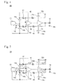
- Fig. 1 is a circuit diagram of a DA conversion device 80 according to the prelude.
- the DA conversion device 80 includes a current output type DA converter 81.
- An output terminal of the DA converter 81 is connected to an inverting input terminal of an operational amplifier 82.
- the inverting input terminal of the operational amplifier 82 is connected to an output terminal of the operational amplifier 82 via a resistor 83 and these constituents collectively form a closed feedback loop (a closed loop). Meanwhile, a non-inverting input terminal of the operational amplifier 82 is connected to a grounding conductor 88c.
- a first power supply 88a and a second power supply 88b are connected to the operational amplifier 82 and the DA converter 81.
- the first power supply 88a generates a positive voltage V on the basis of potential of the grounding conductor 88c while the second power supply 88b generates a negative voltage -V on the basis of the potential of the grounding conductor 88c.
- an output current from the DA converter 81 flows into the output terminal of the operational amplifier 82 via the resistor 83.
- the operational amplifier 82 operates under a closed-loop condition and therefore controls a voltage at the output terminal in such a manner that the voltage at the inverting input terminal becomes equal to the voltage at the non-inverting input terminal. For this reason, a voltage corresponding to a product of the output current from the DA converter 81 and a resistance value of the resistor 83 is outputted from the output terminal of the operational amplifier 82.
- the DA conversion device 80 when the DA conversion device 80 is used as a drive circuit for an electrostatic deflector in an electron beam exposure system or the like, the DA conversion device 80 is required to output a high voltage of ⁇ 40 V or ⁇ 250 V, for example. In this case, a high-voltage operational amplifier needs to be used as the operational amplifier 82.
- a commercially available operational amplifier with a withstand voltage of about ⁇ 6 V has a gain bandwidth of about 500 MHz whereas an operational amplifier with a withstand voltage of about ⁇ 40 V merely has a gain bandwidth of about 100 MHz.
- the high-voltage amplifier has a low operating speed.
- the DA conversion device 80 using the operational amplifier which operates at a high voltage causes a voltage fluctuation such as voltage overshoot or ringing after a change in the output voltage.
- a long settling time is required for settling such a voltage fluctuation, and it is therefore difficult to operate the DA conversion device 80 at a high speed.
- Fig. 2 is a circuit diagram of a DA conversion device according to Example 1.
- a DA conversion device 10 of this example includes the following active elements, namely, a DA converter 11, a high-speed operational amplifier 12, and a buffer amplifier 13.
- the DA converter 11 is a current output type DA converter and its output terminal is connected to a non-inverting input terminal of the high-speed operational amplifier 12.
- the high-speed operational amplifier 12 is an operational amplifier which has a relatively low withstand voltage of several volts but operates at a high speed equivalent to a gain bandwidth of at least several hundreds of megahertz.
- a commercially available operational amplifier having a withstand voltage of about ⁇ 5V and a gain bandwidth of about 600 MHz can be used as the high-speed operational amplifier 12.
- An output terminal of the high-speed operational amplifier 12 is connected to the buffer amplifier 13 while an inverting input terminal of the high-speed operational amplifier 12 is connected to an output terminal of the buffer amplifier 13. Thus, a closed loop is formed. Meanwhile, a resistor 16 is connected between the non-inverting input terminal of the high-speed operational amplifier 12 and a grounding conductor 18c.
- the output terminal of the buffer amplifier 13 is connected to an external output unit 19 with which the DA conversion device 10 is connected to an external device.
- the buffer amplifier 13 is a power amplifier circuit which operates at a relatively high power supply voltage ranging from several tens of volts to several hundreds of volts.
- a push-pull circuit using a pair of a p-type transistor and an n-type transistor, or a high-voltage operational amplifier having a gain set to about 1 can be used as the buffer amplifier 13.
- a first power supply 18a and a second power supply 18b are connected to the buffer amplifier 13.
- the first power supply 18a generates a positive voltage V 1 + relative to the grounding conductor 18c while the second power supply 18b generates a negative voltage V 1 - relative to the grounding conductor 18c.
- the voltages V 1 + and V 1 - are relatively high voltages such as ⁇ 40 V or ⁇ 250 V.
- the DA conversion device 10 of this example further includes a first floating power supply 14a and a second floating power supply 14b, which are independent from the first power supply 18a and the second power supply 18b.
- Batteries can be used as the first floating power supply 14a and the second floating power supply 14b, for example.
- the first and second floating power supplies 14a and 14b are connected in series while interposing a midpoint 14c in between.
- the first floating power supply 14a generates a positive voltage V 2 + on the basis of potential at the midpoint 14c while the second floating power supply 14b generates a negative voltage V 2 - on the basis of the potential at the midpoint 14c.
- the power from each of the floating power supplies 14a and 14b is supplied to the DA converter 11 and the high-speed operational amplifier 12, whereby the DA converter 11 and the high-speed operational amplifier 12 operate on the basis of the potential at the midpoint 14c.
- the voltages of the floating power supplies 14a and 14b are not particularly limited and may be appropriately set according to the withstand voltage of the available operational amplifier.
- the voltages can be set to about ⁇ 5 V, for example.
- the midpoint 14c in the DA conversion device 10 of this example is connected to the output terminal of the buffer amplifier 13. Accordingly, the potential at the midpoint 14c relative to the grounding conductor 18c varies depending on an output voltage from the buffer amplifier 13.
- the DA converter 11 and the high-speed operational amplifier 12 operate mainly based on the potential at the output terminal of the buffer amplifier 13.
- Fig. 3 is a circuit diagram showing the operation of the DA conversion device 10.
- the DA converter 11 outputs a predetermined current is on the basis of an inputted digital signal.
- the outputted current is flows into the grounding conductor 18c via the resistor 16.
- the current is further flows to the output terminal of the buffer amplifier 13 via the first power supply 18a and then back to the DA converter 11 via the corresponding midpoint 14c and the first floating power supply 14a.
- the current is generates a potential difference between the two ends of the resistor 16.
- the potential at the non-inverting input terminal of the high-speed operational amplifier 12 becomes higher than the potential at the grounding conductor 18c.
- the output from the high-speed operational amplifier 12 is increased whereby the voltage at the output terminal of the buffer amplifier 13 is increased. Since the high-speed operational amplifier 12 operates in the state of the closed loop with the buffer amplifier 13, the output terminal of the buffer amplifier 13 and the non-inverting input terminal of the high-speed operational amplifier 12 have the same voltage. In addition, a voltage equal to a product of the output current is from the DA converter 11 and a resistance value of the resistor 16 is outputted from the external output unit 19 of the DA conversion device 10.
- the high-speed operational amplifier 12 and the DA converter 11 operate mainly based on the potential at the output terminal of the buffer amplifier 13.
- the DA conversion device which is capable of outputting a high voltage and is excellent in high-speed performance.
- Fig. 4 is a circuit diagram showing a DA conversion device according to Example 2.
- a DA conversion device 20 of this example can obtain positive and negative output voltages even when a direction of an output current from a DA converter is unchangeable.
- the DA conversion device 20 includes a DA converter 21, the high-speed operational amplifier 12, the buffer amplifier 13, the floating power supplies 14a and 14b, and first to fourth resistors 41, 42, 43, and 44.
- the first and second floating power supplies 14a and 14b are connected in series while interposing a midpoint 14c in between.
- the midpoint 14c is connected to the output terminal of the buffer amplifier 13 via the serially connected third resistor 43 and the fourth resistor 44.
- a positive electrode of the first floating power supply 14a is connected to the grounding conductor 18c via the serially connected first resistor 41 and the second resistor 42.
- the DA converter 21 is a differential current output type DA converter. One of output terminals of the DA converter 21 is connected to the non-inverting input terminal of the high-speed operational amplifier 12 while the other output terminal is connected to the midpoint 14c.
- the non-inverting input terminal of the high-speed operational amplifier 12 is connected between the first resistor 41 and the second resistor 42 while the inverting input terminal of the high-speed operational amplifier 12 is connected between the third resistor 43 and the fourth resistor 44.
- the output terminal of the high-speed operational amplifier 12 is connected to the buffer amplifier 13.
- the output terminal of the buffer amplifier 13 is connected to the external output unit 19.
- This buffer amplifier 13 operates by using the power from the first power supply 18a and the second power supply 18b.
- Fig. 5 is a circuit diagram for explaining the operation of the DA conversion device 20 shown in Fig. 4 .
- a current i s + having a direction indicated with an arrow is outputted from one of the output terminals of the DA converter 21 while a current i s - having a direction indicated with another arrow is outputted from the other output terminal.
- the current i s + flows in from the first resistor 41 and subtracts an amount i s + from a bias current i b which flows from the positive floating power supply 14a toward the grounding conductor 18c.
- the remaining current (i b - i s + ) flows on the second resistor 42.
- the current (i b - i s + ) flows on a route from the grounding conductor 18c, then through the first power supply 18a, the buffer amplifier 13, the fourth resistor 44, the third resistor 43, and to the midpoint 14c as indicated with arrows in Fig. 5 .
- the current i s + passes through the DA converter 21, then flows to the midpoint 14c as a current i s - , and merges with the current (i b - i s + ) at the midpoint 14c.
- the output terminal of the high-speed operational amplifier 12 is connected to the non-inverting input terminal thereof via the buffer amplifier 13 and the fourth resistor 44. These constituents collectively form a closed loop. As a consequence, the voltage at the inverting input terminal of the high-speed operational amplifier 12 also becomes equal to 0 V which is the same potential as that of the non-inverting input terminal thereof.
- the output current from the DA converter 21 is defined as i s + and resistance values of the first to fourth resistors 41, 42, 43, and 44 are defined as R 1 , R 2 , R 3 , and R 4 , respectively.
- the potential at the non-inverting input terminal of the high-speed operational amplifier 12 is defined as V i + and the potential at the inverting input terminal thereof is defined as V i - .
- the potential at the buffer amplifier 13 is defined as v o .
- the potential at the midpoint 14c between the floating power supplies is defined as V f . Note that each potential cited above represents the potential based on the grounding conductor 18c.
- the voltage (an electromotive force) of the first floating power supply 14a is defined as V 2 + and the voltage (an electromotive force) of the second power supply 14b is defined as V 2 - .
- the bias current flowing from the first floating power supply 14a to the first resistor 41 is defined as i b .
- the bias current i b is found in the first place. Focusing on the fact that the non-inverting input terminal and the inverting input terminal of the high-speed operational amplifier 12 have the same potential, the bias current i b can be expressed by the following Formula 1 using the resistance values of the first resistor 41 and the third resistor 43 as well as the output current i s + from the DA converter 21.
- i b V 2 + - R 3 ⁇ i b - i s + R 1
- the bias current i b is determined as in the following Formula 2 by solving Formula 1 for the value i b .
- i b V 2 + - i s + ⁇ R 3 R 1 + R 3
- V i + V 2 + - i s + ⁇ R 3 R 1 + R 3 - i s + ⁇ R 2
- V o R 4 ⁇ i b - i s + + V i +
- V f V i + - R 3 ⁇ i b - i s +
- the following table shows calculation results of the potential V o at the external output unit 19 and the potential V f at the midpoint 14c on the premise that R 1 is set to 1 k ⁇ , R 2 is set to 4 k ⁇ , R 3 is set to 5 ⁇ , R 4 is set to 20 ⁇ , the voltage V 2 + of the first floating power supply 14a is set to 5 V, and the voltage V 2 - of the second floating power supply 14b is set to -5 V, respectively.
- a gain of the high-speed operational amplifier 12 is set to 8e buffer amplifier 13 is set to 0.99.
- the above calculation results prove that the potential at the output terminal of the buffer amplifier 13 varies in a range from 20 [V] to -20 [V] with respect to the output current from the DA converter 21 in a range from 0 to 10 [mA].
- the calculation results also prove that the potential V f at the midpoint 14c, based on which the high-speed operational amplifier 12 and the DA converter 21 operate, varies according to the potential V o at the output terminal of the buffer amplifier 13.
- the high-speed operational amplifier 12 operates normally even when the potential V o at the output terminal of the buffer amplifier 13 greatly exceeds the operating voltage of the high-speed operational amplifier 12. Hence, the settling time is reduced and the operating speed is increased.
- positive and negative output voltages can be obtained from the output of the DA converter 21, which is unable to change the direction of the output current i s + , by appropriately setting the resistance values of the first to fourth resistors 41 to 44.
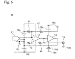
- Fig, 6 is a circuit diagram of a DA conversion device according to Example 3.
- a DA conversion device 30 of Fig. 6 the same constituents as those in the DA conversion device 20 of Fig. 4 will be denoted by the same reference numerals and detailed description thereof will be omitted.
- the DA conversion device 30 of this example is similar to the DA conversion device 20 of Fig. 4 in that the device 30 includes the DA converter 21, the floating power supplies 14a and 14b, the first to fourth resistors 41, 42, 43, and 44, the high-speed operational amplifier 12, and the buffer amplifier 13.
- the non-inverting input terminal of the high-speed operational amplifier 12 is connected to the output terminal of the high-speed operational amplifier 12 via the fourth resistor 44, and the buffer amplifier 13 is therefore excluded from the feedback loop of the high-speed operational amplifier 12.
- the output terminal of the high-speed operational amplifier 12 is connected to the external output unit 19 of the DA conversion device 30.
- the output terminal of the buffer amplifier 13 is connected only to the midpoint 14c between the floating power supplies. Accordingly, the output from the buffer amplifier 13 is used solely for control of the potential at the midpoint 14c between the floating power supplies.
- the potential at the midpoint 14c between the floating power supplies varies with the output from the buffer amplifier 13.
- the high-voltage output can be controlled by use of the high-speed operational amplifier 12, and the operating speed can be increased as a consequence.
- Fig. 7 is a block diagram of an electron beam exposure system according to Example 4.
- An electron beam exposure system 90 shown in Fig. 7 is broadly divided into an exposure section 100 and a control section 160 which controls the exposure section 100.
- the exposure section 100 includes an electron beam generation unit 130, a mask deflection unit 140, and a substrate deflection unit 150.
- an electron gun 101 generates an electron beam EB, and a first electron lens 102 converges this electron beam EB to form the electron beam EB with a predetermined current density.
- the converged electron beam EB further passes through a rectangular aperture 103a in a beam forming mask 103 and is thereby formed to have a rectangular section.
- the electron beam EB thus generated by the electron beam generation unit 130 is focused on an exposure mask 110 with a second electron lens 105 of the mask deflection unit 140. Then, the electron beam EB is deflected by a first electrostatic deflector 104 and a second electrostatic deflector 106 into a shape of a specific pattern S i formed on the exposure mask 110. As the electron beam EB passes through the exposure mask 110, the sectional shape of the electron beam EB is formed into the shape of the pattern S i .
- the electron beam EB having passed through the exposure mask 110 is returned to an optical axis C by a third electrostatic deflector 112 and a fourth electrostatic deflector 113, and is then downsized by a fifth electromagnetic lens 114.
- Deflection aberrations of the electron beam EB caused by the electrostatic deflectors 104, 106, 112, and 113 of the mask deflection unit 140 are corrected by a first correction coil 107 and a second correction coil 109.
- the electron beam EB passes through an aperture 115a in a masking shield 115 provided in the substrate deflection unit 150 and is deflected to a predetermined position on a wafer 212 by a fifth electrostatic deflector 119 and an electromagnetic deflector 120. Then, the electron beam EB is projected onto a surface of the wafer 212 through a first projection electromagnetic lens 116 and a second projection electromagnetic lens 121.
- a third correction coil 117 and a fourth correction coil 118 correct deflection aberrations of the electron beam EB caused by the deflectors 119 and 120 of the substrate deflection unit 150.
- an image of the pattern S i on the exposure mask 110 is transferred onto the wafer 212 at a predetermined reduction ratio such as 1/20.
- control section 160 controls the units of the electron optical system included in the exposure section 100.
- the control section 160 includes any of the DA conversion device 10 (see Fig. 2 ), the DA conversion device 20 (see Fig. 4 ), and the DA conversion device 30 (see Fig. 6 ) as a circuit for generating voltages to be applied to the first to fifth electrostatic deflectors 104, 106, 112, 113, and 119.
- the electron beam exposure system 90 of this example can apply voltages to the electrostatic deflectors by using the DA conversion device which is excellent in terms of the operating speed. Accordingly, settling time for stabilization of the voltages on the electrostatic deflectors is substantially reduced.
- the electron beam exposure system 90 can perform deflection of the electron beam more promptly and thereby improve throughput.
Landscapes
- Chemical & Material Sciences (AREA)
- Analytical Chemistry (AREA)
- Engineering & Computer Science (AREA)
- Theoretical Computer Science (AREA)
- Amplifiers (AREA)
- Analogue/Digital Conversion (AREA)
Abstract
Description
- The embodiments discussed herein are related to a digital-to-analog (DA) conversion device and an electron beam exposure system using the same.
- A DA conversion device requiring high-speed performance includes a current output type DA converter which can be easily increased in speed. The device converts an output current from the DA converter into a voltage with a current-voltage conversion circuit formed of an operational amplifier, and then outputs the voltage thus obtained.
- In the meantime, an electron beam deflection circuit in an electron beam exposure system and the like, or a control circuit in a MRI (magnetic resonance imaging) apparatus and the like may sometimes require a relatively high output voltage ranging from several tens of volts to several hundreds of volts, for example.
- In a DA conversion device used for such applications, a current-voltage conversion circuit adopts an operational amplifier which is operable at a high voltage.
- However, commercially available high-voltage operational amplifiers have a low operating speed and may cause restriction in operating speed of such a DA conversion device.
- Japanese Laid-open Patent Publication No.
2010-193259 - In view of the above, it is an object of the present invention to provide a DA conversion device which is capable of outputting a high voltage and is excellent in terms of an operating speed.
- A first aspect of the invention provides a DA conversion device including: a current output type DA converter; an operational amplifier including a non-inverting input terminal connected to the DA converter and an inverting input terminal connected to an external output unit to output an output signal to outside, and being configured to generate a voltage at the external output unit, the voltage corresponding to an output current from the DA converter; a buffer amplifier connected to an output terminal of the operational amplifier; and floating power supplies configured to respectively supply positive and negative power supply voltages to the DA converter and the operational amplifier, a midpoint between the positive and negative power supplies being connected to an output terminal of the buffer amplifier.
- Meanwhile, another aspect of the invention provides an electron beam exposure system including: an electron gun configured to emit an electron beam; an electrostatic deflector configured to deflect the electron beam; and a control section configured to control a voltage to be applied to the electrostatic deflector. In the system, the control section includes a DA conversion device having: a current output type DA converter; an operational amplifier having a non-inverting input terminal connected to the DA converter and an inverting input terminal connected to an external output unit to output an output signal to outside, and being configured to generate a voltage at the external output unit, the voltage corresponding to an output current from the DA converter; a buffer amplifier connected to an output terminal of the operational amplifier; and floating power supplies configured to respectively supply positive and negative power supply voltages to the DA converter and the operational amplifier, and a midpoint (14c) between the positive and negative power supplies is connected to an output terminal of the buffer amplifier.
- According to the DA conversion device of the above-described aspect, the DA converter and the operational amplifier configured to convert an output current from the DA converter into a voltage are driven by the floating power supplies each having the potential which varies with the output voltage from the buffer amplifier.
- As a consequence, the operational amplifier operates normally even if the output voltage from the buffer amplifier greatly exceeds a withstand voltage of the operational amplifier. Thus, the output voltage from the external output unit can be controlled by using the operational amplifier having a low withstand voltage and an excellent operating speed.
- Accordingly, it is possible to obtain a DA conversion device which enables reduction in settling time for stabilization of an output voltage, is capable of outputting a high voltage, and is excellent in terms of an operating speed.
- Meanwhile, by applying the DA conversion device of the above-described aspect to the control circuit for the electrostatic deflector, a scanning speed of the electron beam is increased whereby productivity of the electron beam exposure system is improved.
-
-
Fig. 1 is a circuit diagram of a DA conversion device according to a prelude. -
Fig. 2 is a circuit diagram of a DA conversion device according to Example 1. -
Fig. 3 is a circuit diagram showing an operation of the DA conversion device ofFig. 1 . -
Fig. 4 is a circuit diagram of a DA conversion device according to Example 2. -
Fig. 5 is a circuit diagram showing an operation of the DA conversion device ofFig. 4 . -
Fig. 6 is a circuit diagram of a DA conversion device according to Example 3. -
Fig. 7 is a block diagram of an electron beam exposure system according to Example 4. - A prelude will be explained before description of embodiments.
-
Fig. 1 is a circuit diagram of aDA conversion device 80 according to the prelude. - The
DA conversion device 80 includes a current outputtype DA converter 81. An output terminal of theDA converter 81 is connected to an inverting input terminal of anoperational amplifier 82. The inverting input terminal of theoperational amplifier 82 is connected to an output terminal of theoperational amplifier 82 via aresistor 83 and these constituents collectively form a closed feedback loop (a closed loop). Meanwhile, a non-inverting input terminal of theoperational amplifier 82 is connected to agrounding conductor 88c. - A
first power supply 88a and asecond power supply 88b are connected to theoperational amplifier 82 and theDA converter 81. Thefirst power supply 88a generates a positive voltage V on the basis of potential of thegrounding conductor 88c while thesecond power supply 88b generates a negative voltage -V on the basis of the potential of thegrounding conductor 88c. - In the
DA conversion device 80, an output current from theDA converter 81 flows into the output terminal of theoperational amplifier 82 via theresistor 83. - The
operational amplifier 82 operates under a closed-loop condition and therefore controls a voltage at the output terminal in such a manner that the voltage at the inverting input terminal becomes equal to the voltage at the non-inverting input terminal. For this reason, a voltage corresponding to a product of the output current from theDA converter 81 and a resistance value of theresistor 83 is outputted from the output terminal of theoperational amplifier 82. - In this way, the output current from the
DA converter 81 is converted into the voltage by theoperational amplifier 82. - In the meantime, when the
DA conversion device 80 is used as a drive circuit for an electrostatic deflector in an electron beam exposure system or the like, theDA conversion device 80 is required to output a high voltage of ±40 V or ±250 V, for example. In this case, a high-voltage operational amplifier needs to be used as theoperational amplifier 82. - However, commercially available high-voltage operational amplifiers have shortcomings of low operating speeds.
- For instance, a commercially available operational amplifier with a withstand voltage of about ±6 V has a gain bandwidth of about 500 MHz whereas an operational amplifier with a withstand voltage of about ±40 V merely has a gain bandwidth of about 100 MHz. Thus, the high-voltage amplifier has a low operating speed.
- As a consequence, the
DA conversion device 80 using the operational amplifier which operates at a high voltage causes a voltage fluctuation such as voltage overshoot or ringing after a change in the output voltage. A long settling time is required for settling such a voltage fluctuation, and it is therefore difficult to operate theDA conversion device 80 at a high speed. - Now, examples of the invention will be described.
-
Fig. 2 is a circuit diagram of a DA conversion device according to Example 1. - As shown in
Fig. 2 , aDA conversion device 10 of this example includes the following active elements, namely, aDA converter 11, a high-speedoperational amplifier 12, and abuffer amplifier 13. - The
DA converter 11 is a current output type DA converter and its output terminal is connected to a non-inverting input terminal of the high-speedoperational amplifier 12. - The high-speed
operational amplifier 12 is an operational amplifier which has a relatively low withstand voltage of several volts but operates at a high speed equivalent to a gain bandwidth of at least several hundreds of megahertz. For example, a commercially available operational amplifier having a withstand voltage of about ±5V and a gain bandwidth of about 600 MHz can be used as the high-speedoperational amplifier 12. - An output terminal of the high-speed
operational amplifier 12 is connected to thebuffer amplifier 13 while an inverting input terminal of the high-speedoperational amplifier 12 is connected to an output terminal of thebuffer amplifier 13. Thus, a closed loop is formed. Meanwhile, aresistor 16 is connected between the non-inverting input terminal of the high-speedoperational amplifier 12 and agrounding conductor 18c. - The output terminal of the
buffer amplifier 13 is connected to anexternal output unit 19 with which theDA conversion device 10 is connected to an external device. Thebuffer amplifier 13 is a power amplifier circuit which operates at a relatively high power supply voltage ranging from several tens of volts to several hundreds of volts. For example, a push-pull circuit using a pair of a p-type transistor and an n-type transistor, or a high-voltage operational amplifier having a gain set to about 1 can be used as thebuffer amplifier 13. - A
first power supply 18a and asecond power supply 18b are connected to thebuffer amplifier 13. Thefirst power supply 18a generates a positive voltage V1 + relative to thegrounding conductor 18c while thesecond power supply 18b generates a negative voltage V1 - relative to thegrounding conductor 18c. The voltages V1 + and V1 - are relatively high voltages such as ±40 V or ± 250 V. - The
DA conversion device 10 of this example further includes a first floatingpower supply 14a and a second floatingpower supply 14b, which are independent from thefirst power supply 18a and thesecond power supply 18b. - Batteries can be used as the first floating
power supply 14a and the second floatingpower supply 14b, for example. The first and second floatingpower supplies midpoint 14c in between. The first floatingpower supply 14a generates a positive voltage V2 + on the basis of potential at themidpoint 14c while the second floatingpower supply 14b generates a negative voltage V2 - on the basis of the potential at themidpoint 14c. - The power from each of the floating
power supplies DA converter 11 and the high-speedoperational amplifier 12, whereby theDA converter 11 and the high-speedoperational amplifier 12 operate on the basis of the potential at themidpoint 14c. - The voltages of the floating
power supplies - Moreover, the
midpoint 14c in theDA conversion device 10 of this example is connected to the output terminal of thebuffer amplifier 13. Accordingly, the potential at themidpoint 14c relative to thegrounding conductor 18c varies depending on an output voltage from thebuffer amplifier 13. - Accordingly, the
DA converter 11 and the high-speedoperational amplifier 12 operate mainly based on the potential at the output terminal of thebuffer amplifier 13. - Now, an operation of the
DA conversion device 10 will be described below.Fig. 3 is a circuit diagram showing the operation of theDA conversion device 10. - As shown in
Fig. 3 , theDA converter 11 outputs a predetermined current is on the basis of an inputted digital signal. The outputted current is flows into thegrounding conductor 18c via theresistor 16. The current is further flows to the output terminal of thebuffer amplifier 13 via thefirst power supply 18a and then back to theDA converter 11 via the correspondingmidpoint 14c and the first floatingpower supply 14a. - The current is generates a potential difference between the two ends of the
resistor 16. As a consequence, the potential at the non-inverting input terminal of the high-speedoperational amplifier 12 becomes higher than the potential at thegrounding conductor 18c. - Thus, the output from the high-speed
operational amplifier 12 is increased whereby the voltage at the output terminal of thebuffer amplifier 13 is increased. Since the high-speedoperational amplifier 12 operates in the state of the closed loop with thebuffer amplifier 13, the output terminal of thebuffer amplifier 13 and the non-inverting input terminal of the high-speedoperational amplifier 12 have the same voltage. In addition, a voltage equal to a product of the output current is from theDA converter 11 and a resistance value of theresistor 16 is outputted from theexternal output unit 19 of theDA conversion device 10. - During this process, the potential at the
midpoint 14c changes according to the potential at the output terminal of thebuffer amplifier 13. Thus, the high-speedoperational amplifier 12 and theDA converter 11 operate mainly based on the potential at the output terminal of thebuffer amplifier 13. - Accordingly, even when the potential at the output terminal of the
buffer amplifier 13 greatly exceeds the withstand voltage of the high-speedoperational amplifier 12, no voltage in excess of the withstand voltage is applied to the high-speedoperational amplifier 12 and therefore the high-speedoperational amplifier 12 operates normally. - As a result, voltage overshoot or ringing which may occur in a high-voltage operational amplifier is promptly settled by feedback control of the high-speed
operational amplifier 12, whereby settling time for stabilization of the output voltage is remarkably reduced. - Hence, it is possible to obtain the DA conversion device which is capable of outputting a high voltage and is excellent in high-speed performance.
-
Fig. 4 is a circuit diagram showing a DA conversion device according to Example 2. - A
DA conversion device 20 of this example can obtain positive and negative output voltages even when a direction of an output current from a DA converter is unchangeable. - Now, constituents of the
DA conversion device 20 will be described below. Note that the constituents inFig. 4 which are similar to those in theDA conversion device 10 ofFig. 2 will be denoted by the same reference numerals and detailed description thereof will be omitted. - As shown in
Fig. 4 , theDA conversion device 20 includes aDA converter 21, the high-speedoperational amplifier 12, thebuffer amplifier 13, the floatingpower supplies fourth resistors - The first and second floating
power supplies midpoint 14c in between. Themidpoint 14c is connected to the output terminal of thebuffer amplifier 13 via the serially connectedthird resistor 43 and thefourth resistor 44. - Meanwhile, a positive electrode of the first floating
power supply 14a is connected to thegrounding conductor 18c via the serially connectedfirst resistor 41 and thesecond resistor 42. - The
DA converter 21 is a differential current output type DA converter. One of output terminals of theDA converter 21 is connected to the non-inverting input terminal of the high-speedoperational amplifier 12 while the other output terminal is connected to themidpoint 14c. - The non-inverting input terminal of the high-speed
operational amplifier 12 is connected between thefirst resistor 41 and thesecond resistor 42 while the inverting input terminal of the high-speedoperational amplifier 12 is connected between thethird resistor 43 and thefourth resistor 44. In addition, the output terminal of the high-speedoperational amplifier 12 is connected to thebuffer amplifier 13. - Meanwhile, the output terminal of the
buffer amplifier 13 is connected to theexternal output unit 19. Thisbuffer amplifier 13 operates by using the power from thefirst power supply 18a and thesecond power supply 18b. - Now, an operation of the
DA conversion device 20 will be described.Fig. 5 is a circuit diagram for explaining the operation of theDA conversion device 20 shown inFig. 4 . - As shown in
Fig. 5 , a current is + having a direction indicated with an arrow is outputted from one of the output terminals of theDA converter 21 while a current is - having a direction indicated with another arrow is outputted from the other output terminal. - The current is + flows in from the
first resistor 41 and subtracts an amount is + from a bias current ib which flows from the positive floatingpower supply 14a toward thegrounding conductor 18c. The remaining current (ib - is +) flows on thesecond resistor 42. - The current (ib - is +) flows on a route from the
grounding conductor 18c, then through thefirst power supply 18a, thebuffer amplifier 13, thefourth resistor 44, thethird resistor 43, and to themidpoint 14c as indicated with arrows inFig. 5 . - In the meantime, the current is + passes through the
DA converter 21, then flows to themidpoint 14c as a current is -, and merges with the current (ib - is +) at themidpoint 14c. - Here, when (ib - is +) = 0 holds true, the current flowing on the
second resistor 42 becomes 0 and no potential difference is generated at thesecond resistor 42. For this reason, the potential at the non-inverting input terminal of the high-speedoperational amplifier 12 becomes 0 V which is the same potential as that of thegrounding conductor 18c. - The output terminal of the high-speed
operational amplifier 12 is connected to the non-inverting input terminal thereof via thebuffer amplifier 13 and thefourth resistor 44. These constituents collectively form a closed loop. As a consequence, the voltage at the inverting input terminal of the high-speedoperational amplifier 12 also becomes equal to 0 V which is the same potential as that of the non-inverting input terminal thereof. - In this state, no current flows on the
third resistor 43 and the potential at themidpoint 14c between the floating power supplies becomes equal to 0 V which is the same as that of thegrounding conductor 18c. - When current outputs is + and is - are changed from this state, voltage outputs corresponding to the amounts of the change in the currents are obtained.
- Now, a change in the output voltage corresponding to the change in the outputted current is + from the
DA converter 21 will be described below. - Here, the output current from the
DA converter 21 is defined as is + and resistance values of the first tofourth resistors operational amplifier 12 is defined as Vi + and the potential at the inverting input terminal thereof is defined as Vi -. The potential at thebuffer amplifier 13 is defined as vo. Further, the potential at themidpoint 14c between the floating power supplies is defined as Vf. Note that each potential cited above represents the potential based on thegrounding conductor 18c. - In the meantime, the voltage (an electromotive force) of the first floating
power supply 14a is defined as V2 + and the voltage (an electromotive force) of thesecond power supply 14b is defined as V2 -. Meanwhile, the bias current flowing from the first floatingpower supply 14a to thefirst resistor 41 is defined as ib. - The bias current ib is found in the first place. Focusing on the fact that the non-inverting input terminal and the inverting input terminal of the high-speed
operational amplifier 12 have the same potential, the bias current ib can be expressed by the following Formula 1 using the resistance values of thefirst resistor 41 and thethird resistor 43 as well as the output current is + from theDA converter 21.
- The bias current ib is determined as in the following Formula 2 by solving Formula 1 for the value ib.

- Next, the potential Vi + at the non-inverting input terminal of the high-speed
operational amplifier 12 is found. - The input of the high-speed
operational amplifier 12 has high impedance, so that the entire current (ib - is +) is deemed to flow on thesecond resistor 42. Accordingly, the potential Vi + at the non-inverting input terminal of the high-speedoperational amplifier 12 is expressed by the following Formula 3.
- The potential Vi + at the non-inverting input terminal is found as in the following Formula 4 by assigning Formula 2 to Formula 3.

- Meanwhile, the potential Vo at the output terminal of the
buffer amplifier 13 is expressed by the following Formula 5.
- The following Formula 6 expressing the potential Vo at the output terminal of the
buffer amplifier 13 is obtained by assigning Formula 2 to Formula 5 and performing adjustment as appropriate.
- At this time, the potential Vf at the
midpoint 14c between the floating power supplies, which serves as an operation reference point of the high-speedoperational amplifier 12, is expressed by the following Formula 7.
- The following Formula 8 expressing the potential Vf at the
midpoint 14c is obtained by assigning Formula 2 and Formula 4 to Formula 7.
- Comparison between Formula 6 which expresses the potential Vo at the output terminal of the
buffer amplifier 13 and Formula 8 which expresses the potential Vf at themidpoint 14c proves that the potential Vf at themidpoint 14c varies with the potential Vo at the output terminal. - The following table shows calculation results of the potential Vo at the
external output unit 19 and the potential Vf at themidpoint 14c on the premise that R1 is set to 1 kΩ, R2 is set to 4 kΩ, R3 is set to 5 Ω, R4 is set to 20 Ω, the voltage V2 + of the first floatingpower supply 14a is set to 5 V, and the voltage V2 - of the second floatingpower supply 14b is set to -5 V, respectively. - Upon the calculation, a gain of the high-speed
operational amplifier 12 is set to 8ebuffer amplifier 13 is set to 0.99.[Table 1] is + [mA] Vo [V] Vf [V] 0 20 19.87562 2.5 10 9.93781 5 0 0 7.5 -10 -9.9378 10 -20 -19.87562 - The above calculation results prove that the potential at the output terminal of the
buffer amplifier 13 varies in a range from 20 [V] to -20 [V] with respect to the output current from theDA converter 21 in a range from 0 to 10 [mA]. The calculation results also prove that the potential Vf at themidpoint 14c, based on which the high-speedoperational amplifier 12 and theDA converter 21 operate, varies according to the potential Vo at the output terminal of thebuffer amplifier 13. - Accordingly, in the
DA conversion device 20 of this example as well, the high-speedoperational amplifier 12 operates normally even when the potential Vo at the output terminal of thebuffer amplifier 13 greatly exceeds the operating voltage of the high-speedoperational amplifier 12. Hence, the settling time is reduced and the operating speed is increased. - Moreover, in the
DA conversion device 20 of this example, positive and negative output voltages can be obtained from the output of theDA converter 21, which is unable to change the direction of the output current is +, by appropriately setting the resistance values of the first tofourth resistors 41 to 44. -
Fig, 6 is a circuit diagram of a DA conversion device according to Example 3. In aDA conversion device 30 ofFig. 6 , the same constituents as those in theDA conversion device 20 ofFig. 4 will be denoted by the same reference numerals and detailed description thereof will be omitted. - As shown in
Fig. 6 , theDA conversion device 30 of this example is similar to theDA conversion device 20 ofFig. 4 in that thedevice 30 includes theDA converter 21, the floatingpower supplies fourth resistors operational amplifier 12, and thebuffer amplifier 13. - Meanwhile, the non-inverting input terminal of the high-speed
operational amplifier 12 is connected to the output terminal of the high-speedoperational amplifier 12 via thefourth resistor 44, and thebuffer amplifier 13 is therefore excluded from the feedback loop of the high-speedoperational amplifier 12. In addition, the output terminal of the high-speedoperational amplifier 12 is connected to theexternal output unit 19 of theDA conversion device 30. - Further, the output terminal of the
buffer amplifier 13 is connected only to themidpoint 14c between the floating power supplies. Accordingly, the output from thebuffer amplifier 13 is used solely for control of the potential at themidpoint 14c between the floating power supplies. - In the
DA conversion device 30 described above as well, the potential at themidpoint 14c between the floating power supplies varies with the output from thebuffer amplifier 13. Thus, the high-voltage output can be controlled by use of the high-speedoperational amplifier 12, and the operating speed can be increased as a consequence. -
Fig. 7 is a block diagram of an electron beam exposure system according to Example 4. - An electron
beam exposure system 90 shown inFig. 7 is broadly divided into anexposure section 100 and acontrol section 160 which controls theexposure section 100. Of the sections, theexposure section 100 includes an electronbeam generation unit 130, amask deflection unit 140, and asubstrate deflection unit 150. - In the electron
beam generation unit 130, anelectron gun 101 generates an electron beam EB, and afirst electron lens 102 converges this electron beam EB to form the electron beam EB with a predetermined current density. The converged electron beam EB further passes through arectangular aperture 103a in abeam forming mask 103 and is thereby formed to have a rectangular section. - The electron beam EB thus generated by the electron
beam generation unit 130 is focused on anexposure mask 110 with asecond electron lens 105 of themask deflection unit 140. Then, the electron beam EB is deflected by a first electrostatic deflector 104 and a secondelectrostatic deflector 106 into a shape of a specific pattern Si formed on theexposure mask 110. As the electron beam EB passes through theexposure mask 110, the sectional shape of the electron beam EB is formed into the shape of the pattern Si. - The electron beam EB having passed through the
exposure mask 110 is returned to an optical axis C by a thirdelectrostatic deflector 112 and a fourthelectrostatic deflector 113, and is then downsized by a fifthelectromagnetic lens 114. - Deflection aberrations of the electron beam EB caused by the
electrostatic deflectors mask deflection unit 140 are corrected by afirst correction coil 107 and asecond correction coil 109. - Thereafter, the electron beam EB passes through an
aperture 115a in amasking shield 115 provided in thesubstrate deflection unit 150 and is deflected to a predetermined position on awafer 212 by a fifthelectrostatic deflector 119 and anelectromagnetic deflector 120. Then, the electron beam EB is projected onto a surface of thewafer 212 through a first projectionelectromagnetic lens 116 and a second projectionelectromagnetic lens 121. - A
third correction coil 117 and afourth correction coil 118 correct deflection aberrations of the electron beam EB caused by thedeflectors substrate deflection unit 150. - With the above-described electron optical system, an image of the pattern Si on the
exposure mask 110 is transferred onto thewafer 212 at a predetermined reduction ratio such as 1/20. - In the meantime, the
control section 160 controls the units of the electron optical system included in theexposure section 100. - The
control section 160 includes any of the DA conversion device 10 (seeFig. 2 ), the DA conversion device 20 (seeFig. 4 ), and the DA conversion device 30 (seeFig. 6 ) as a circuit for generating voltages to be applied to the first to fifthelectrostatic deflectors - In this way, the electron
beam exposure system 90 of this example can apply voltages to the electrostatic deflectors by using the DA conversion device which is excellent in terms of the operating speed. Accordingly, settling time for stabilization of the voltages on the electrostatic deflectors is substantially reduced. - As a consequence, the electron
beam exposure system 90 can perform deflection of the electron beam more promptly and thereby improve throughput.
Claims (7)
A DA conversion device (10, 20, 30) comprising:
The DA conversion device (10, 20, 30) according to claim 1, further comprising
power supply devices (18a, 18b) configured to respectively supply positive and negative power supply voltages to the buffer amplifier (13),
wherein
an absolute value of the power supply voltages from the power supply devices (18a, 18b) to the buffer amplifier (13) is greater than an absolute value of the power supply voltages from the floating power supplies (14a, 14b).
The DA conversion device (20, 30) according to claim 2, further comprising
a resistor (42) connected between a grounding conductor (18c) for the power supply devices (18a, 18b) for the buffer amplifier (13) and the non-inverting input terminal of the operational amplifier (12).
The DA conversion device (20, 30) according to claim 2, further comprising:
wherein
the non-inverting input terminal of the operational amplifier (12) is connected to an output terminal of the DA converter (21) and is connected between the first resistor (41) and the second resistor (42), and
the inverting input terminal of the operational amplifier (12) is connected between the third resistor (43) and the fourth resistor (44).
The DA conversion device (20) according to claim 4, wherein the output terminal of the buffer amplifier (13) is connected to the external output unit (19).
The DA conversion device (30) according to claim 4, wherein the output terminal of the operational amplifier (12) is connected to the external output unit (19).
An electron beam exposure system (90) comprising:
and
floating power supplies (14a, 14b) configured to respectively supply positive and negative power supply voltages to the DA converter (11) and the operational amplifier (12), wherein
Applications Claiming Priority (1)
| Application Number | Priority Date | Filing Date | Title |
|---|---|---|---|
| JP2012091762A JP5438161B2 (en) | 2012-04-13 | 2012-04-13 | DA converter |
Publications (1)
| Publication Number | Publication Date |
|---|---|
| EP2651037A2 true EP2651037A2 (en) | 2013-10-16 |
Family
ID=47143031
Family Applications (1)
| Application Number | Title | Priority Date | Filing Date |
|---|---|---|---|
| EP12191833.8A Withdrawn EP2651037A2 (en) | 2012-04-13 | 2012-11-08 | DA conversion device and electron beam exposure system using the same |
Country Status (3)
| Country | Link |
|---|---|
| US (1) | US8618970B2 (en) |
| EP (1) | EP2651037A2 (en) |
| JP (1) | JP5438161B2 (en) |
Families Citing this family (2)
| Publication number | Priority date | Publication date | Assignee | Title |
|---|---|---|---|---|
| US8933414B2 (en) * | 2013-02-27 | 2015-01-13 | Fei Company | Focused ion beam low kV enhancement |
| JP6294651B2 (en) * | 2013-12-11 | 2018-03-14 | 株式会社日立情報通信エンジニアリング | Reference waveform generation circuit, apparatus, and method |
Citations (1)
| Publication number | Priority date | Publication date | Assignee | Title |
|---|---|---|---|---|
| JP2010193259A (en) | 2009-02-19 | 2010-09-02 | Dkk Toa Corp | High voltage output type amplifier |
Family Cites Families (22)
| Publication number | Priority date | Publication date | Assignee | Title |
|---|---|---|---|---|
| JPS5829220A (en) * | 1981-08-14 | 1983-02-21 | Fuji Xerox Co Ltd | Analog voltage output device |
| US4692579A (en) * | 1984-05-18 | 1987-09-08 | Hitachi, Ltd. | Electron beam lithography apparatus |
| JP2553032B2 (en) * | 1985-03-19 | 1996-11-13 | 株式会社ニコン | Charged particle beam deflection circuit |
| US4644253A (en) * | 1986-02-13 | 1987-02-17 | Analog Devices, Inc. | Voltage reference source with true ground sensing and force-sense outputs referred thereto |
| JPS6474789A (en) | 1987-09-16 | 1989-03-20 | Nec Corp | Semiconductor laser device |
| JPH0661853A (en) * | 1992-08-10 | 1994-03-04 | Sony Corp | Electronic device |
| JPH07325112A (en) * | 1994-05-31 | 1995-12-12 | Sony Tektronix Corp | Load current detecting circuit |
| JPH1074789A (en) | 1996-08-29 | 1998-03-17 | Shinkawa Ltd | Abnormal load detector for bonding equipment |
| JPH10239661A (en) * | 1997-02-26 | 1998-09-11 | Sony Corp | Liquid crystal display |
| JP3969463B2 (en) * | 1997-04-14 | 2007-09-05 | 富士通株式会社 | Charged particle beam exposure method and apparatus |
| JPH1174789A (en) * | 1997-08-29 | 1999-03-16 | Rohm Co Ltd | A/d converter measuring device |
| JP2000099168A (en) * | 1998-09-22 | 2000-04-07 | Yokogawa Electric Corp | Floating power supply |
| JP2006173807A (en) * | 2004-12-13 | 2006-06-29 | Sanyo Electric Co Ltd | A/d converter |
| JP4534808B2 (en) * | 2005-03-11 | 2010-09-01 | 横河電機株式会社 | Amplifier circuit with current limiter |
| JP4652214B2 (en) * | 2005-11-18 | 2011-03-16 | 富士通セミコンダクター株式会社 | Analog to digital converter |
| CN101432630B (en) * | 2006-04-28 | 2010-12-08 | 爱德万测试株式会社 | Power applying circuit and testing apparatus |
| JP2008070307A (en) * | 2006-09-15 | 2008-03-27 | Agilent Technol Inc | Capacity measuring device and capacity measuring method |
| TW200841602A (en) * | 2007-04-09 | 2008-10-16 | Realtek Semiconductor Corp | Digital-to-analog converter and method |
| JP4710879B2 (en) * | 2007-06-25 | 2011-06-29 | ヤマハ株式会社 | Digital amplifier device |
| WO2009066371A1 (en) * | 2007-11-20 | 2009-05-28 | Advantest Corporation | D/a converter and electron beam lithography system |
| US7898447B2 (en) * | 2009-07-16 | 2011-03-01 | Nuflare Technology, Inc. | Methods and systems for testing digital-to-analog converter/amplifier circuits |
| JP5576332B2 (en) * | 2011-04-06 | 2014-08-20 | 株式会社アドバンテスト | Electron beam exposure apparatus and electron beam exposure method |
-
2012
- 2012-04-13 JP JP2012091762A patent/JP5438161B2/en active Active
- 2012-11-08 EP EP12191833.8A patent/EP2651037A2/en not_active Withdrawn
- 2012-11-20 US US13/682,311 patent/US8618970B2/en active Active
Patent Citations (1)
| Publication number | Priority date | Publication date | Assignee | Title |
|---|---|---|---|---|
| JP2010193259A (en) | 2009-02-19 | 2010-09-02 | Dkk Toa Corp | High voltage output type amplifier |
Also Published As
| Publication number | Publication date |
|---|---|
| JP5438161B2 (en) | 2014-03-12 |
| JP2013223003A (en) | 2013-10-28 |
| US8618970B2 (en) | 2013-12-31 |
| US20130270449A1 (en) | 2013-10-17 |
Similar Documents
| Publication | Publication Date | Title |
|---|---|---|
| KR101921351B1 (en) | Multiple-pole electrostatic deflector for improving throughput of focused electron beam instruments | |
| JP3932894B2 (en) | Electron beam equipment | |
| JP2009054581A (en) | Orbit corrector for charged particle beam and charged particle beam apparatus | |
| US6642675B2 (en) | Charged particle beam exposing apparatus | |
| JP2872420B2 (en) | Method and apparatus for charged particle beam exposure | |
| US8618970B2 (en) | DA conversion device and electron beam exposure system using the same | |
| US20070075887A1 (en) | Electrostatic particle beam deflector | |
| US4249112A (en) | Dynamic focus and astigmatism correction circuit | |
| JP2019215976A (en) | Charged particle beam control apparatus | |
| JP3485888B2 (en) | Electron beam writing apparatus and semiconductor device manufactured using the same | |
| CN119132915A (en) | Magnetic deflection control system and scanning electron microscope | |
| KR102931355B1 (en) | Focused ion beam apparatus and method for controlling the same | |
| JP5462569B2 (en) | Electron beam exposure system | |
| JP6817349B2 (en) | Deflector and charged particle beam device | |
| KR20240116649A (en) | Multi-charged particle beam drawing device | |
| JP6163255B2 (en) | Charged particle beam apparatus and spherical aberration correction method | |
| JP2901246B2 (en) | Charged particle beam exposure system | |
| US4891523A (en) | Circuit for image displacement in a particle beam apparatus independently of magnification | |
| JP3969463B2 (en) | Charged particle beam exposure method and apparatus | |
| US6388516B1 (en) | Precision high speed magnetic coil driver circuit | |
| JP5107629B2 (en) | Deflection control circuit and electron beam scanning device | |
| JPH09102448A (en) | Charged particle beam exposure method and apparatus | |
| JP2914926B2 (en) | Charged particle beam exposure method | |
| JP2010219444A (en) | Charged particle beam drawing device | |
| CN116745880A (en) | Electron optics array and methods of directing the primary electron beam onto the sample |
Legal Events
| Date | Code | Title | Description |
|---|---|---|---|
| PUAI | Public reference made under article 153(3) epc to a published international application that has entered the european phase |
Free format text: ORIGINAL CODE: 0009012 |
|
| 17P | Request for examination filed |
Effective date: 20121108 |
|
| AK | Designated contracting states |
Kind code of ref document: A2 Designated state(s): AL AT BE BG CH CY CZ DE DK EE ES FI FR GB GR HR HU IE IS IT LI LT LU LV MC MK MT NL NO PL PT RO RS SE SI SK SM TR |
|
| AX | Request for extension of the european patent |
Extension state: BA ME |
|
| RAP1 | Party data changed (applicant data changed or rights of an application transferred) |
Owner name: HITACHI INFORMATION & TELECOMMUNICATION ENGINEERIN Owner name: ADVANTEST CORPORATION |
|
| STAA | Information on the status of an ep patent application or granted ep patent |
Free format text: STATUS: THE APPLICATION HAS BEEN WITHDRAWN |
|
| 18W | Application withdrawn |
Effective date: 20150918 |