EP2651024B1 - Multilevel power converter - Google Patents
Multilevel power converter Download PDFInfo
- Publication number
- EP2651024B1 EP2651024B1 EP13153220.2A EP13153220A EP2651024B1 EP 2651024 B1 EP2651024 B1 EP 2651024B1 EP 13153220 A EP13153220 A EP 13153220A EP 2651024 B1 EP2651024 B1 EP 2651024B1
- Authority
- EP
- European Patent Office
- Prior art keywords
- voltage
- semiconductor
- terminal
- capacitor
- power supply
- Prior art date
- Legal status (The legal status is an assumption and is not a legal conclusion. Google has not performed a legal analysis and makes no representation as to the accuracy of the status listed.)
- Active
Links
- 239000004065 semiconductor Substances 0.000 claims description 235
- 239000003990 capacitor Substances 0.000 claims description 110
- 230000002457 bidirectional effect Effects 0.000 claims description 76
- 230000000903 blocking effect Effects 0.000 claims description 5
- 238000006243 chemical reaction Methods 0.000 description 46
- 238000005516 engineering process Methods 0.000 description 6
- 238000010586 diagram Methods 0.000 description 4
- 238000010276 construction Methods 0.000 description 3
- 238000004519 manufacturing process Methods 0.000 description 2
- 230000003247 decreasing effect Effects 0.000 description 1
- 230000006866 deterioration Effects 0.000 description 1
- 230000007935 neutral effect Effects 0.000 description 1
- 238000004513 sizing Methods 0.000 description 1
- 230000007704 transition Effects 0.000 description 1
Images

Classifications
-
- H—ELECTRICITY
- H02—GENERATION; CONVERSION OR DISTRIBUTION OF ELECTRIC POWER
- H02M—APPARATUS FOR CONVERSION BETWEEN AC AND AC, BETWEEN AC AND DC, OR BETWEEN DC AND DC, AND FOR USE WITH MAINS OR SIMILAR POWER SUPPLY SYSTEMS; CONVERSION OF DC OR AC INPUT POWER INTO SURGE OUTPUT POWER; CONTROL OR REGULATION THEREOF
- H02M7/00—Conversion of ac power input into dc power output; Conversion of dc power input into ac power output
- H02M7/42—Conversion of dc power input into ac power output without possibility of reversal
- H02M7/44—Conversion of dc power input into ac power output without possibility of reversal by static converters
- H02M7/48—Conversion of dc power input into ac power output without possibility of reversal by static converters using discharge tubes with control electrode or semiconductor devices with control electrode
- H02M7/483—Converters with outputs that each can have more than two voltages levels
- H02M7/487—Neutral point clamped inverters
-
- H—ELECTRICITY
- H02—GENERATION; CONVERSION OR DISTRIBUTION OF ELECTRIC POWER
- H02M—APPARATUS FOR CONVERSION BETWEEN AC AND AC, BETWEEN AC AND DC, OR BETWEEN DC AND DC, AND FOR USE WITH MAINS OR SIMILAR POWER SUPPLY SYSTEMS; CONVERSION OF DC OR AC INPUT POWER INTO SURGE OUTPUT POWER; CONTROL OR REGULATION THEREOF
- H02M7/00—Conversion of ac power input into dc power output; Conversion of dc power input into ac power output
- H02M7/42—Conversion of dc power input into ac power output without possibility of reversal
- H02M7/44—Conversion of dc power input into ac power output without possibility of reversal by static converters
- H02M7/48—Conversion of dc power input into ac power output without possibility of reversal by static converters using discharge tubes with control electrode or semiconductor devices with control electrode
- H02M7/483—Converters with outputs that each can have more than two voltages levels
- H02M7/4837—Flying capacitor converters
-
- H—ELECTRICITY
- H02—GENERATION; CONVERSION OR DISTRIBUTION OF ELECTRIC POWER
- H02M—APPARATUS FOR CONVERSION BETWEEN AC AND AC, BETWEEN AC AND DC, OR BETWEEN DC AND DC, AND FOR USE WITH MAINS OR SIMILAR POWER SUPPLY SYSTEMS; CONVERSION OF DC OR AC INPUT POWER INTO SURGE OUTPUT POWER; CONTROL OR REGULATION THEREOF
- H02M1/00—Details of apparatus for conversion
- H02M1/0095—Hybrid converter topologies, e.g. NPC mixed with flying capacitor, thyristor converter mixed with MMC or charge pump mixed with buck
Definitions
- the present invention relates to a semiconductor power converter technology, and in particular, to a technology to construct a multilevel power conversion circuit that directly outputs a plurality of voltage levels.
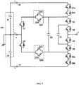
- FIG. 7 shows an example of seven level power conversion circuit according to a conventional technology disclosed in Patent Document 1.
- the circuit of FIG. 7 is a partial circuit for one phase of a multilevel, seven level in the conventional circuit of FIG. 7 , power conversion circuit.
- a single phase conversion circuit can be composed by using two partial circuits of FIG. 7 and a three phase conversion circuit can be composed by using three partial circuits of FIG. 7 .
- a DC power supply assembly BA2 comprises series-connected single DC power supplies b11, b12, b13, b21, b22, and b23.
- the DC power supply assembly BA2 has seven terminals P1, P2, P3, M, N1, N2, and N3 at seven different voltage levels.
- a series connection circuit of semiconductor switches Q1 through Q12 which are IGBTs in this example, is connected between the positive terminal P3 and the negative terminal N3.
- the connection point of the semiconductors Q6 and Q7 is connected to an AC output terminal U.
- a diode arm pair DA1 composed of series-connected diodes D1 and D2 is connected between the connection point of the semiconductor switches Q1 and Q2 and the connection point of the semiconductor switches Q7 and Q8.
- the middle terminal of the diode arm pair DA1 is connected to the connection point of the single DC power supplies b11 and b12.
- a diode arm pair DA2 composed of series-connected diodes D3 and D4 is connected between the connection point of the semiconductor switches Q2 and Q3 and the connection point of the semiconductor switches Q8 and Q9.
- the middle terminal of the diode arm pair DA2 is connected to the connection point of the single DC power supplies b12 and b13.
- a diode arm pair DA3 composed of series-connected diodes D5 and D6 is connected between the connection point of the semiconductor switches Q3 and Q4 and the connection point of the semiconductor switches Q9 and Q10.
- the middle terminal of the diode arm pair DA3 is connected to the connection point of the single DC power supplies b13 and b21.
- the diode arm pair DA4 composed of series-connected diodes D7 and D8 is connected between the connection point of the semiconductor switches Q4 and Q5 and the connection point of the semiconductor switches Q10 and Q11.
- the middle terminal of the diode arm pair DA4 is connected to the connection point of the single DC power supplies b21 and b22.
- a diode arm pair DA5 composed of series-connected diodes D9 and D10 is connected between the connection point of the semiconductor switches Q5 and Q6 and the connection point of the semiconductor switches Q11 and Q12.
- the middle terminal of the diode arm pair DA5 is connected to the connection point of the single DC power supplies b22 and b23.
- the AC terminal U when the semiconductor switches Q1 through Q6 are in the ON state and the semiconductor switches Q7 through Q12 are in the OFF state, the AC terminal U outputs a voltage +3E; when the semiconductor switches Q2 through Q7 are in the ON state and the semiconductor switches Q8 through Q12 and Q1 are in the OFF state, the AC terminal U outputs a voltage +2E; when the semiconductor switches Q3 through Q8 are in the ON state and the semiconductor switches Q9 through Q12 and Q1 and Q2 are in the OFF state, the AC terminal U outputs a voltage +1E; when the semiconductor switches Q4 through Q9 are in the ON state and the semiconductor switches Q10 through Q12 and Q1 through Q3 are in the OFF state, the AC terminal U outputs a voltage 0 (zero); when the semiconductor switches Q5 through Q10 are in the ON state and the semiconductor switches Q11 and Q12 and Q1 through Q4 are in the OFF state, the AC terminal U outputs a voltage -1E; when the semiconductor switches Q6 through Q11 are in the
- the DC power supply assembly BA2 an input device of the multilevel power conversion circuit, needs six single DC power supplies each delivering a power independently, which imposes a severe limitation in production of the device.
- the problem of unbalance of DC power supplies is disclosed in IEEE-PESC 1995 Conference Record pp. 1144-1150 entitled "A multi-level voltage source converter system with balanced DC voltage .”
- Patent application JP2010246189 discloses a multilevel power converter comprising a flying capacitor cell and an active neutral point clamp (ANPC).
- a multilevel power converter for converting DC power to AC power or AC power to DC power of the first aspect of the present invention comprises: a DC power supply assembly having first and second single DC power supplies connected in series, and three terminals of a positive terminal, a negative terminal, and a middle point terminal at a middle electric potential between the positive terminal and the negative terminal; a first semiconductor series circuit composed of first through sixth semiconductor switches, each having an antiparallel-connected diode, connected in series in this order between the positive terminal and the negative terminal of the DC power supply assembly; a second semiconductor series circuit composed of a first bidirectional switch, seventh and eighth semiconductor switches each having an antiparallel-connected diode, and second bidirectional switch connected in series in this order between a connection point of the first semiconductor switch and the second semiconductor switch and the connection point of the fifth semiconductor switch and the sixth semiconductor switch; a first capacitor connected in parallel with a series circuit of the third semiconductor switch and the fourth semiconductor switch; and a second capacitor connected in parallel with the second semiconductor switch series circuit; wherein
- the multilevel power converter of the second aspect of the present invention is the multilevel power converter device of the first aspect of the present invention, wherein the first semiconductor switch or the sixth semiconductor switch is composed of a plurality of semiconductor switches having the same function connected in series and the series-connected semiconductor switches are each driven with a different control signal.
- the multilevel power converter of the third aspect of the present invention is the multilevel power converter of the first or second aspect of the invention, wherein the first bidirectional switch or the second bidirectional switch is composed of semiconductor elements having reverse blocking ability in antiparallel connection and the antiparallel-connected semiconductor elements are each driven with a different control signal.
- the multilevel power converter device of the fourth aspect of the present invention is the multilevel power converter of the first or second aspect of the invention, wherein the first bidirectional switch or the second bidirectional switch is composed of semiconductor switches that are series-connected with each other in an anti-series mode and each of the semiconductor switches has an antiparallel connected diode and driven with a different control signal.
- the multilevel power converter device of the fifth aspect of the present invention is the multilevel power converter of any one of the first through fourth aspects of the invention, wherein the multilevel power converter uses the DC power supply assembly having the three terminals at voltage levels of +3E, 0, and -3E, holds the first capacitor at a voltage of 1E and the second capacitor at a voltage of 2E, generates seven levels of voltages of +3E, +2E, +1E, 0, -1E, -2E, and -3E utilizing voltages of the DC power supply assembly, the first capacitor, and the second capacitor, and delivers any voltage selected from the seven levels of voltages to the AC terminal.
- the multilevel power converter uses the DC power supply assembly having the three terminals at voltage levels of +3E, 0, and -3E, holds the first capacitor at a voltage of 1E and the second capacitor at a voltage of 2E, generates seven levels of voltages of +3E, +2E, +1E, 0, -1E, -2E, and -3E utilizing voltages of the DC power
- the present invention reduces the number of semiconductor switches carrying the current from the input DC power supply assembly to the AC output terminal from six at the maximum to four at the maximum, thus decreasing power loss. This results in higher efficiency, lower cost, and smaller size.
- the input DC power supply assembly can be composed of only two single DC power supplies, which eliminates the limitation imposed on the conventional circuit, making equipment production easier.
- the essential point of the present invention is as follows.
- a multilevel power converter of the present invention comprises: a DC power supply assembly having a positive terminal, a zero terminal, and a negative terminal; a first semiconductor switch series circuit composed of first through sixth semiconductor switches connected in series in this order between the positive terminal and the negative terminal; a second semiconductor switch series circuit composed of a first bidirectional switch, seventh and eighth semiconductor switches, and a second bidirectional switch connected in series in this order between the connection point of the first and second semiconductor switches and the connection point of the fifth and sixth semiconductor switches; a first capacitor connected in parallel with a series circuit of the third and fourth semiconductor switches; and a second capacitor connected in parallel with the second semiconductor switch series circuit; wherein the zero terminal of the DC power supply assembly is connected to the connection point of the seventh and eighth semiconductor switches and an AC terminal is connected to the connection point of the third and fourth semiconductor switches.
- FIG. 1 shows a first embodiment of the present invention.
- the circuit of FIG. 1 is one phase of a power conversion circuit that uses a DC power supply circuit of the DC power supply assembly BA1 having three terminals of a positive terminal, a zero terminal, and a negative terminal and comprising series-connected single DC power supplies b1 and b2.
- This multilevel power conversion circuit comprises a first semiconductor switch series circuit composed of series-connected semiconductor switches Q1 through Q6 connected between the positive terminal P and the negative terminal N of the DC power supply assembly BA1, and a first capacitor C1 connected in parallel with a series circuit of semiconductor switches Q3 and Q4.
- a second capacitor C2 is connected between the connection point of semiconductor switches Q1 and Q2 and the connection point of semiconductor switches Q5 and Q6.
- a second semiconductor switch series circuit is connected in parallel with the second capacitor C2.
- the second semiconductor switch series circuit comprises a bidirectional switch SW1, the semiconductor switches Q7 and Q8, and another bidirectional switch SW2 connected in series.
- the connection point of the semiconductor switches Q7 and Q8 is connected to the zero terminal M of the DC power supply assembly BA1, and the connection point of the semiconductor switches Q3 and Q4 is connected to the AC terminal U.
- the switching mode 1 delivers +3E at the AC terminal U.
- the semiconductor switches Q1, Q2, and Q3 are in the ON state and the semiconductor switch Q4 and the QR1 of the bidirectional switch SW1 are in the OFF state.
- the output current flows through the path: the single DC power supply b1 ⁇ the semiconductor switch Q1 ⁇ the semiconductor switch Q2 ⁇ the semiconductor switch Q3 ⁇ the AC terminal U.
- the current passes through three semiconductor switches: Q1, Q2, and Q3.
- the voltage undergone by the semiconductor switch Q4 is equal to the voltage VC1 across the capacitor C1, 1E, in the condition of OFF states of the semiconductor switches Q5, Q6, and Q7 and the QR3 of the bidirectional switch SW2.
- the series-connected circuit of the semiconductor switch Q7 and the bidirectional switch SW1 is subjected to a voltage of 3E that is the voltage Vb1 of the single DC power supply b1.
- the semiconductor switch Q7 and the bidirectional switch SW1 of the series circuit thereof exhibit withstand voltages with a ratio of two to one, the semiconductor switch Q7 is subjected to a voltage of 2E and the bidirectional switch SW1 is subjected to a voltage of 1E.
- the voltage at the AC terminal U is +3E under the conditions of: using the DC power supply assembly BA1 with the voltage Vb1 of the single DC power supply b1 of 3E and the voltage Vb2 of the single DC power supply b2 of -3E, and holding the voltage VC1 of the capacitor C1 at 1E and the voltage VC2 of the capacitor C2 at 2E.
- the bidirectional switches SW1 and SW2 and semiconductor switches Q4, Q5, Q6, and Q7 are subjected to the voltages 1E, 1E, 1E, 1E, 4E, and 2E, respectively.
- the switching mode 2 delivers +2E at the AC terminal U.
- the semiconductor switches Q1, Q2, and Q4 are in the ON state and the semiconductor switches Q3, Q5, Q6, and Q7, and QR1 of the bidirectional switch SW1 and QR3 of the bidirectional switch SW2 are in the OFF state.
- the output current flows through the path: the single DC power supply b1 ⁇ the semiconductor switch Q1 ⁇ the semiconductor switch Q2 ⁇ the capacitor C1 ⁇ the semiconductor switch Q4 ⁇ the AC terminal U.
- the current passes through three semiconductor switches Q1, Q2, and Q4.
- the AC terminal U delivers a voltage of 2E that is the voltage Vb1 of the single DC power supply b1 subtracted by the voltage VC1 of the capacitor C1.
- the semiconductor switch Q3 is subjected to a voltage of 1E that is the voltage VC1; the semiconductor switch Q5 is subjected to a voltage of 1E that is the voltage VC2 of the capacitor C2 subtracted by the voltage VC1 of the capacitor C1; the semiconductor switch Q6 is subjected to a voltage of 4E that is the voltage -Vb2 of the single DC power supply b2 + the voltage Vb1 of the single DC power supply b1 - the voltage VC2 of the capacitor C2; the bidirectional switch SW2 is subjected to a voltage of 1E that is the voltage Vb1 of the single DC power supply b1 subtracted by the voltage VC2 of the capacitor C2; and the series-connected circuit of the semiconductor switch Q7 and the bidirectional switch SW1 is subjected to the voltage Vb1 of the single DC power supply b1. These components are clamped at the voltages indicated above.
- the voltage at the AC terminal U is +2E under the conditions of: using the DC power supply assembly BA1 with the voltage Vb1 of the single DC power supply b1 of 3E and the voltage Vb2 of the single DC power supply b2 of -3E, and holding the voltage VC1 of the capacitor C1 at 1E and the voltage VC2 of the capacitor C2 at 2E.
- the bidirectional switches SW1 and SW2 and the semiconductor switches Q3, Q5, Q6, and Q7 are subjected to the voltages 1E, 1E, 1E, 1E, 4E, and 2E, respectively.
- the switching mode 3 delivers +2E at the AC terminal U.
- the semiconductor switches Q1, Q3, and Q5 are in the ON state and the semiconductor switches Q2, Q4, Q6, and Q7, and QR1 of the bidirectional switch SW1 and QR3 of the bidirectional switch SW2 are in the OFF state.
- the output current flows through the path: the single DC power supply b1 ⁇ the semiconductor switch Q1 ⁇ the capacitor C2 ⁇ the semiconductor switch Q5 ⁇ the capacitor C1 ⁇ the semiconductor switch Q3 ⁇ the AC terminal U.
- the current passes through three semiconductor switches Q1, Q5, and Q3.
- the AC terminal U delivers a voltage that is the voltage Vb1 of the single DC power supply b1 - the voltage VC2 of the capacitor C2 + the voltage VC1 of the capacitor C1.
- the voltage at the AC terminal U is +2E under the conditions of: using the DC power supply assembly BA1 with the voltage Vb1 of the single DC power supply b1 of 3E and the voltage Vb2 of the single DC power supply b2 of -3E, and holding the voltage VC1 of the capacitor C1 at 1E and the voltage VC2 of the capacitor C2 at 2E.
- the bidirectional switches SW1 and SW2 and the semiconductor switches Q2, Q4, Q6, and Q7 are clamped at the voltages 1E, 1E, 1E, 1E, 4E, and 2E, respectively.
- the switching mode 4 delivers +2E at the AC terminal U.
- the bidirectional switches SW1 and SW2 and the semiconductor switches Q2, Q3, and Q8 are in the ON state, and the semiconductor switches Q1, Q4, Q5, Q6, and Q7 are in the OFF state.
- the output current flows through the path: the zero terminal of the DC power supply assembly BA1 ⁇ the semiconductor switch Q8 ⁇ the bidirectional switch SW2 ⁇ the capacitor C2 ⁇ the semiconductor switch Q2 ⁇ the semiconductor switch Q3 ⁇ the AC terminal U.
- the current passes through four switches of the bidirectional switch SW2 and the semiconductor switches Q8, Q2, and Q3.
- the AC terminal U delivers directly a voltage of 2E that is the voltage VC2 of the capacitor C2.
- the voltage at the AC terminal U is +2E under the conditions of: using the DC power supply assembly BA1 with the voltage Vb1 of the single DC power supply b1 of 3E and the voltage Vb2 of the single DC power supply b2 of -3E, and holding the voltage VC1 of the capacitor C1 at 1E and the voltage VC2 of the capacitor C2 at 2E.
- the semiconductor switches Q1, Q4, Q5, Q6, and Q7 are clamped at the voltages 1E, 1E, 1E, 3E, and 2E, respectively.
- the switching mode 5 delivers +1E at the AC terminal U.
- the semiconductor switches Q1, Q4, and Q5 are in the ON state, and the semiconductor switches Q2, Q3, Q6, and Q7 and the QR1 of the bidirectional switch SW1, and the QR3 of the bidirectional switch SW2 are in the OFF state.
- the output current flows through the path: the single DC power supply b1 ⁇ the semiconductor switch Q1 ⁇ the capacitor C2 ⁇ the semiconductor switch Q5 ⁇ the semiconductor switch Q4 ⁇ the AC terminal U.
- the current passes through three switches of the semiconductor switches Q1, Q5, and Q4.
- the AC terminal U delivers a voltage of 1E that is the voltage Vb1 of the single DC power supply b1 - the voltage VC2 of the capacitor C2.
- the voltage at the AC terminal U is +1E under the conditions of: using the DC power supply assembly BA1 with the voltage Vb1 of the single DC power supply b1 of 3E and the voltage Vb2 of the single DC power supply b2 of -3E, and holding the voltage VC1 of the capacitor C1 at 1E and the voltage VC2 of the capacitor C2 at 2E.
- the bidirectional switches SW1 and SW2, the semiconductor switches Q2, Q3, Q6, and Q7 are clamped at the voltages 1E, 1E, 1E, 1E, 4E, and 2E, respectively.
- the switching mode 6 with the assumption of seven level power conversion circuit as described above, delivers +1E at the AC terminal U.
- the bidirectional switches SW1 and SW2, the semiconductor switches Q2, Q4, and Q8 are in the ON state, and the semiconductor switches Q1, Q3, Q5, Q6, and Q7 are in the OFF state.
- the output current flows through the path: the zero terminal M of the DC power supply assembly BA1 ⁇ the semiconductor switch Q8 ⁇ the bidirectional switch SW2 ⁇ the capacitor C2 ⁇ the semiconductor switch Q2 ⁇ the capacitor C1 ⁇ the semiconductor switch Q4 ⁇ the AC terminal U.
- the current passes through four switches of the semiconductor switches Q8, Q2, and Q4 and the bidirectional switch SW2.
- the AC terminal U delivers a voltage of 1E that is the voltage VC2 of the capacitor C2 - the voltage VC1 of the capacitor C1.
- the voltage at the AC terminal U is +1E under the conditions of: using the DC power supply assembly BA1 with the voltage Vb1 of the single DC power supply b1 of 3E and the voltage Vb2 of the single DC power supply b2 of -3E, and holding the voltage VC1 of the capacitor C1 at 1E and the voltage VC2 of the capacitor C2 at 2E.
- the semiconductor switches Q1, Q3, Q5, Q6, and Q7 are clamped at the voltages 1E, 1E, 1E, 3E, and 2E, respectively.
- the switching mode 7 delivers +1E at the AC terminal U.
- the bidirectional switches SW1 and SW2 the semiconductor switches Q3, Q5, and Q8 are in the ON state, and the semiconductor switches Q1, Q2, Q4, Q6, and Q7 are in the OFF state.
- the output current flows through the path: the zero terminal M of the DC power supply assembly BA1 ⁇ the semiconductor switch Q8 ⁇ the bidirectional switch SW2 ⁇ the semiconductor switch Q5 ⁇ the capacitor C1 ⁇ semiconductor switch Q3 ⁇ the AC terminal U.
- the current passes through four switches of the semiconductor switches Q8, Q5, and Q3 and the bidirectional switch SW2.
- the AC terminal U delivers a voltage of 1Ed that is the voltage VC1 of the capacitor C1.
- the voltage at the AC terminal U is +1E under the conditions of: using the DC power supply assembly BA1 with the voltage Vb1 of the single DC power supply b1 of 3E and the voltage Vb2 of the single DC power supply b2 of -3E, and holding the voltage VC1 of the capacitor C1 at 1E and the voltage VC2 of the capacitor C2 at 2E.
- the semiconductor switches Q1, Q2, Q4, Q6, and Q7 are clamped at the voltages 1E, 1E, 1E, 3E, and 2E, respectively.
- the switching mode 8 with the assumption of seven level power conversion circuit as described above, delivers 0 (zero) at the AC terminal U.
- the bidirectional switches SW1 and SW2 the semiconductor switches Q4, Q5, and Q8 are in the ON state, and the semiconductor switches Q1, Q2, Q3, Q6, and Q7 are in the OFF state.
- the output current flows through the path: the zero terminal M of the DC power supply assembly BA1 ⁇ the semiconductor switch Q8 ⁇ the bidirectional switch SW2 ⁇ the semiconductor switch Q5 ⁇ the semiconductor switch Q4 ⁇ the AC terminal U.
- the current passes through four switches of the semiconductor switches Q8, Q5, and Q4 and the bidirectional switch SW2.
- the AC terminal U delivers a voltage of 0 (zero) that is the potential at the zero terminal M of the DC power supply assembly BA1.
- the voltage at the AC terminal U is 0 (zero) under the conditions of: using the DC power supply assembly BA1 with the voltage Vb1 of the single DC power supply b1 of 3E and the voltage Vb2 of the single DC power supply b2 of -3E, and holding the voltage VC1 of the capacitor C1 at 1E and the voltage VC2 of the capacitor C2 at 2E.
- the semiconductor switches Q1, Q2, Q3, Q6, and Q7 are clamped at the voltages 1E, 1E, 1E, 3E, and 2E, respectively.
- the switching mode 9 with the assumption of seven level power conversion circuit as described above, delivers 0 (zero) at the AC terminal U.
- the bidirectional switches SW1 and SW2, the semiconductor switches Q2, Q3, and Q7 are in the ON state, and the semiconductor switches Q1, Q4, Q5, Q6, and Q8 are in the OFF state.
- the output current flows through the path: the zero terminal M of the DC power supply assembly BA1 ⁇ the semiconductor switch Q7 ⁇ the bidirectional switch SW1 ⁇ the semiconductor switch Q2 ⁇ the semiconductor switch Q3 ⁇ the AC terminal U.
- the current passes through four switches of the semiconductor switches Q7, Q2, and Q3 and the bidirectional switch SW1.
- the AC terminal U delivers a voltage of 0 (zero) that is the potential at the zero terminal M of the DC power supply assembly BA1.
- the voltage at the AC terminal U is 0 under the conditions of: using the DC power supply assembly BA1 with the voltage Vb1 of the single DC power supply b1 of 3E and the voltage Vb2 of the single DC power supply b2 of -3E, and holding the voltage VC1 of the capacitor C1 at 1E and the voltage VC2 of the capacitor C2 at 2E.
- the semiconductor switches Q1, Q4, Q5, Q6, and Q8 are clamped at the voltages 3E, 1E, 1E, 1E, and 2E, respectively.
- the switching mode 10 delivers -1E at the AC terminal U.
- the bidirectional switches SW1 and SW2, the semiconductor switches Q2, Q4, and Q7 are in the ON state, and the semiconductor switches Q1, Q3, Q5, Q6, and Q8 are in the OFF state.
- the output current flows through the path: the zero terminal M of the DC power supply assembly BA1 ⁇ the semiconductor switch Q7 ⁇ the bidirectional switch SW1 ⁇ the semiconductor switch Q2 ⁇ the capacitor C1 ⁇ the semiconductor switch Q4 ⁇ the AC terminal U.
- the current passes through four switches of the semiconductor switches Q7, Q2, and Q4 and the bidirectional switch SW1.
- the AC terminal U delivers a voltage of -1E that is the voltage - VC1 of the capacitor C1.
- the voltage at the AC terminal U is -1E under the conditions of: using the DC power supply assembly BA1 with the voltage Vb1 of the single DC power supply b1 of 3E and the voltage Vb2 of the single DC power supply b2 of -3E, and holding the voltage VC1 of the capacitor C1 at 1E and the voltage VC2 of the capacitor C2 at 2E.
- the semiconductor switches Q1, Q3, Q5, Q6, and Q8 are clamped at the voltages 3E, 1E, 1E, 1E, and 2E, respectively.
- the switching mode 11 delivers -1E at the AC terminal U.
- the bidirectional switches SW1 and SW2 the semiconductor switches Q3, Q5, and Q7 are in the ON state, and the semiconductor switches Q1, Q2, Q4, Q6, and Q8 are in the OFF state.
- the output current flows through the path: the zero terminal M of the DC power supply assembly BA1 ⁇ the semiconductor switch Q7 ⁇ the bidirectional switch SW1 ⁇ the capacitor C2 ⁇ the semiconductor switch Q5 ⁇ the capacitor C1 ⁇ the semiconductor switch Q3 ⁇ the AC terminal U.
- the current passes through four switches of the semiconductor switches Q7, Q5, and Q3 and the bidirectional switch SW1.
- the AC terminal U delivers a voltage of -1E that is the voltage -VC2 of the capacitor C2 + the voltage VC1 of the capacitor C1.
- the voltage at the AC terminal U is -1E under the conditions of: using the DC power supply assembly BA1 with the voltage Vb1 of the single DC power supply b1 of 3E and the voltage Vb2 of the single DC power supply b2 of -3E, and holding the voltage VC1 of the capacitor C1 at 1E and the voltage VC2 of the capacitor C2 at 2E.
- the semiconductor switches Q1, Q2, Q4, Q6, and Q8 are clamped at the voltages 3E, 1E, 1E, 1E, and 2E, respectively.
- the switching mode 12 delivers -1E at the AC terminal U.
- the semiconductor switches Q2, Q3, and Q6 are in the ON state, and the semiconductor switches Q1, Q4, Q5, and Q8, and the QR1 of the bidirectional switch SW1 and the QR3 of the bidirectional switch SW2 are in the OFF state.
- the output current flows through the path: the single DC power supply b2 ⁇ the semiconductor switch Q6 ⁇ the capacitor C2 ⁇ the semiconductor switch Q2 ⁇ the semiconductor switch Q3 ⁇ the AC terminal U.
- the current passes through three switches of the semiconductor switches Q6, Q2, and Q3.
- the AC terminal U delivers a voltage of -1E that is the voltage Vb2 of the single DC power supply b2 + VC2 of the capacitor C2.
- the voltage at the AC terminal U is -1E under the conditions of: using the DC power supply assembly BA1 with the voltage Vb1 of the single DC power supply b1 of 3E and the voltage Vb2 of the single DC power supply b2 of -3E, and holding the voltage VC1 of the capacitor C1 at 1E and the voltage VC2 of the capacitor C2 at 2E.
- the bidirectional switches SW1 and SW2, semiconductor switches Q1, Q4, Q5, and Q8 are clamped at the voltages 1E, 1E, 4E, 1E, 1E, and 2E, respectively.
- the switching mode 13 delivers -2E at the AC terminal U.
- the bidirectional switches SW1 and SW2, and the semiconductor switches Q4, Q5, and Q7 are in the ON state, and the semiconductor switches Q1, Q2, Q3, Q6, and Q8, are in the OFF state.
- the output current flows through the path: the zero terminal M of the DC power supply assembly BA1 ⁇ the semiconductor switch Q7 ⁇ the bidirectional switch SW1 ⁇ the capacitor C2 ⁇ the semiconductor switch Q5 ⁇ the semiconductor switch Q4 ⁇ the AC terminal U.
- the current passes through four switches of the semiconductor switches Q7, Q5, and Q4 and the bidirectional switch SW1.
- the AC terminal U delivers a voltage of -2E that is the voltage - VC2 of the capacitor C2.
- the voltage at the AC terminal U is -2E under the conditions of: using the DC power supply assembly BA1 with the voltage Vb1 of the single DC power supply b1 of 3E and the voltage Vb2 of the single DC power supply b2 of -3E, and holding the voltage VC1 of the capacitor C1 at 1E and the voltage VC2 of the capacitor C2 at 2E.
- the semiconductor switches Q1, Q2, Q3, Q6, and Q8 are clamped at the voltages 3E, 1E, 1E, 1E, and 2E, respectively.
- the switching mode 14 delivers -2E at the AC terminal U.
- the semiconductor switches Q2, Q4, and Q6 are in the ON state, and the semiconductor switches Q1, Q3, Q5, and Q8, and the QR2 of the bidirectional switch SW1 and the QR4 of the bidirectional switch SW2 are in the OFF state.
- the output current flows through the path: the single DC power supply b2 ⁇ the semiconductor switch Q6 ⁇ the capacitor C2 ⁇ the semiconductor switch Q2 ⁇ the capacitor C1 ⁇ the semiconductor switch Q4 ⁇ the AC terminal U.
- the current passes through three switches of the semiconductor switches Q6, Q2, and Q4.
- the AC terminal U delivers a voltage of -2E that is the voltage Vb2 of the single DC power supply b2 + the voltage VC2 of the capacitor C2 - the voltage VC1 of the capacitor C1.
- the voltage at the AC terminal U is -2E under the conditions of: using the DC power supply assembly BA1 with the voltage Vb1 of the single DC power supply b1 of 3E and the voltage Vb2 of the single DC power supply b2 of -3E, and holding the voltage VC1 of the capacitor C1 at 1E and the voltage VC2 of the capacitor C2 at 2E.
- the bidirectional switches SW1 and SW2 and the semiconductor switches Q1, Q3, Q5, and Q8 are clamped at the voltages 1E, 1E, 4E, 1E, 1E, and 2E, respectively.
- the switching mode 15 delivers -2E at the AC terminal U.
- the semiconductor switches Q3, Q5, and Q6 are in the ON state, and the semiconductor switches Q1, Q2, Q4, and Q8, and the QR2 of the bidirectional switch SW1 and the QR4 of the bidirectional switch SW2 are in the OFF state.
- the output current flows through the path: the single DC power supply b2 ⁇ the semiconductor switch Q6 ⁇ the semiconductor switch Q5 ⁇ the capacitor C1 ⁇ the semiconductor switch Q3 ⁇ the AC terminal U.
- the current passes through three switches of the semiconductor switches Q6, Q5, and Q3.
- the AC terminal U delivers a voltage of -2E that is the voltage Vb2 of the single DC power supply b2 + the voltage VC1 of the capacitor C1.
- the voltage at the AC terminal U is -2E under the conditions of: using the DC power supply assembly BA1 with the voltage Vb1 of the single DC power supply b1 of 3E and the voltage Vb2 of the single DC power supply b2 of -3E, and holding the voltage VC1 of the capacitor C1 at 1E and the voltage VC2 of the capacitor C2 at 2E.
- the bidirectional switches SW1 and SW2 and the semiconductor switches Q1, Q2, Q4, and Q8 are clamped at the voltages 1E, 1E, 4E, 1E, 1E, and 2E, respectively.
- the switching mode 16 delivers -3E at the AC terminal U.
- the semiconductor switches Q4, Q5, and Q6 are in the ON state, and the semiconductor switches Q1, Q2, Q3, and Q8, and the QR2 of the bidirectional switch SW1 and the QR4 of the bidirectional switch SW2 are in the OFF state.
- the output current flows through the path: the single DC power supply b2 ⁇ the semiconductor switch Q6 ⁇ the semiconductor switch Q5 ⁇ the semiconductor switch Q4 ⁇ the AC terminal U.
- the current passes through three switches of the semiconductor switches Q6, Q5, and Q4.
- the AC terminal U delivers a voltage of -3E that is the voltage Vb2 of the single DC power supply b2.
- the voltage at the AC terminal U is -3E under the conditions of: using the DC power supply assembly BA1 with the voltage Vb1 of the single DC power supply b1 of 3E and the voltage Vb2 of the single DC power supply b2 of -3E, and holding the voltage VC1 of the capacitor C1 at 1E and the voltage VC2 of the capacitor C2 at 2E.
- the bidirectional switches SW1 and SW2 and the semiconductor switches Q1, Q2, Q3, and Q8 are clamped at the voltages 1E, 1E, 4E, 1E, 1E, and 2E, respectively.
- the seven level power conversion circuit with the single DC power supplies b1 and b2 delivering voltages Vb1 of +3E and Vb2 of -3E, respectively, can output seven levels of voltages of +3E, +2E, +1E, 0, -1E, -2E, and -3E at the AC terminal U by the switching mode 1 through the switching mode 16.
- the seven level power conversion circuit operates to deliver the same output voltage of +2E in the switching mode 2 through the switching mode 4. However, in the positive direction of the AC output current i from the AC terminal, the switching mode 2 charges the capacitor C1 with the AC output current i; the switching mode 3 discharges the capacitor C1 and charges the capacitor C2; and the switching mode 4 discharges the capacitor C2.
- the same voltage of +1E is delivered from the AC terminal U in the switching mode 5 through switching mode 7.
- the switching mode 5 charges the capacitor C2; the switching mode 6 charges the capacitor C1 and discharges the capacitor C2; and the switching mode 7 discharges the capacitor C1.
- the voltage VC1 of the capacitor C1 and the voltage VC2 of the capacitor C2 can be adjusted independently by appropriately selecting, for delivering a voltage of +2E at the AC output terminal U, a switching mode from the switching modes 2, 3, and 4, and selecting, for delivering a voltage of +1E at the AC terminal U, a switching mode from the switching modes 5, 6, and 7.
- the example of seven level power conversion circuit described above controls the voltage VC1 of the capacitor C1 at 1E and the voltage VC2 of the capacitor C2 at 2E.
- FIG. 4 shows a multilevel power converter circuit according to a second embodiment of the present invention.
- the device of this Embodiment 2 differs from the device of Embodiment 1 in the construction of bidirectional switches SW1 and SW2. While bidirectional switches in the circuit of the Embodiment 1 are constructed by antiparallel connection of reverse blocking semiconductor switches QR1 through QR4, bidirectional switches in Embodiment 2 are constructed by anti-series connection of semiconductor switches QS1 through QS4 without reverse blocking ability.
- the switching of the QS1 is conducted in the same ON/OFF operation as of the QR1; QS2, in the same ON/OFF operation as of the QR2; QS3, in the same ON/OFF operation as of the QR3; and QS4, in the same ON/OFF operation as of the QR4.
- the bidirectional switches SW1 and SW2 perform exactly the same operation and function in both Embodiment 1 and Embodiment 2.
- FIG. 5 shows a multilevel power converter circuit of a third embodiment according to the present invention.
- the device of this Embodiment 3 differs from the device of Embodiment 1 in that the semiconductor switch Q1 in Embodiment 1 is replaced by a series-connected circuit of semiconductor switches Q1a and Q1b in Embodiment 3 and the semiconductor switch Q6 in Embodiment 1 is replaced by a series-connected circuit of semiconductor switches Q6a and Q6b in Embodiment 3.
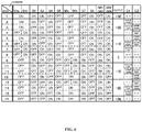
- FIG. 6 shows a seven level operation in the device with the replaced semiconductor switches Q1a, Q1b, Q6a, and Q6b.
- the switching modes 1, 2, 3, and the switching mode 5 the switches Q1a and Q1b are both in the ON state and the switches Q6a and Q6b are both in the OFF state.
- the switching mode 4 and the switching modes 6, 7, and 8 one of the switches Q1a and Q1b is in the ON state and both the Q6a and Q6b are in the OFF state.
- the switching modes 9, 10, 11, and the switching mode 13 the Q1a and Q1b are both in the OFF state and one of the Q6a and Q6b is in the ON state.
- the switching mode 12 and the switching modes 14, 15, and 16, the Q1a and Q1b are both in the OFF state and the Q6a and Q6b are both in the ON state.
- the semiconductor switches Q1 and Q6 in FIG. 1 each of which needs a withstand voltage of at least 4E in principle, can be replaced by the series-connected circuit of the semiconductor switches Q1a and Q1b and by the series-connected circuit of the semiconductor switches Q6a and Q6b, each of the Q1a, Q1b, Q6a, and Q6b being necessary to have only half the withstand voltage of the Q1 and Q6. Transition between the modes in this device is carried out by single switching operation of a semiconductor element of a low withstand voltage, which reduces switching loss and thus achieves lower loss in the device.
- IGBTs of high withstand voltage of in the range of kilovolts or higher for example, switching characteristics and steady-state loss deteriorate rapidly with increase in the withstand voltage.
- This technology of the invention is useful in such a case to reduce power loss employing semiconductor elements of low withstand voltage, which exhibit excellent characteristics
- the devices of the embodiments described thus far are inverters for converting a DC power to an AC power.
- the present invention can be applied to a converter circuit for converting an AC power to a DC power.
- the present invention provides a circuit technology for generating a multilevel AC voltage from a small number of single DC power supplies, and can be applied to high voltage motor driving equipment and power converters for grid-connection.
Landscapes
- Engineering & Computer Science (AREA)
- Power Engineering (AREA)
- Inverter Devices (AREA)
- Rectifiers (AREA)
Description
- The present invention relates to a semiconductor power converter technology, and in particular, to a technology to construct a multilevel power conversion circuit that directly outputs a plurality of voltage levels.
-
FIG. 7 shows an example of seven level power conversion circuit according to a conventional technology disclosed inPatent Document 1. The circuit ofFIG. 7 is a partial circuit for one phase of a multilevel, seven level in the conventional circuit ofFIG. 7 , power conversion circuit. A single phase conversion circuit can be composed by using two partial circuits ofFIG. 7 and a three phase conversion circuit can be composed by using three partial circuits ofFIG. 7 . Referring toFIG. 7 , a DC power supply assembly BA2 comprises series-connected single DC power supplies b11, b12, b13, b21, b22, and b23. The DC power supply assembly BA2 has seven terminals P1, P2, P3, M, N1, N2, and N3 at seven different voltage levels. A series connection circuit of semiconductor switches Q1 through Q12, which are IGBTs in this example, is connected between the positive terminal P3 and the negative terminal N3. The connection point of the semiconductors Q6 and Q7 is connected to an AC output terminal U. A diode arm pair DA1 composed of series-connected diodes D1 and D2 is connected between the connection point of the semiconductor switches Q1 and Q2 and the connection point of the semiconductor switches Q7 and Q8. The middle terminal of the diode arm pair DA1 is connected to the connection point of the single DC power supplies b11 and b12. - Similarly, a diode arm pair DA2 composed of series-connected diodes D3 and D4 is connected between the connection point of the semiconductor switches Q2 and Q3 and the connection point of the semiconductor switches Q8 and Q9. The middle terminal of the diode arm pair DA2 is connected to the connection point of the single DC power supplies b12 and b13.
- A diode arm pair DA3 composed of series-connected diodes D5 and D6 is connected between the connection point of the semiconductor switches Q3 and Q4 and the connection point of the semiconductor switches Q9 and Q10. The middle terminal of the diode arm pair DA3 is connected to the connection point of the single DC power supplies b13 and b21.
- The diode arm pair DA4 composed of series-connected diodes D7 and D8 is connected between the connection point of the semiconductor switches Q4 and Q5 and the connection point of the semiconductor switches Q10 and Q11. The middle terminal of the diode arm pair DA4 is connected to the connection point of the single DC power supplies b21 and b22.
- A diode arm pair DA5 composed of series-connected diodes D9 and D10 is connected between the connection point of the semiconductor switches Q5 and Q6 and the connection point of the semiconductor switches Q11 and Q12. The middle terminal of the diode arm pair DA5 is connected to the connection point of the single DC power supplies b22 and b23.
- In this circuit construction, when the semiconductor switches Q1 through Q6 are in the ON state and the semiconductor switches Q7 through Q12 are in the OFF state, the AC terminal U outputs a voltage +3E; when the semiconductor switches Q2 through Q7 are in the ON state and the semiconductor switches Q8 through Q12 and Q1 are in the OFF state, the AC terminal U outputs a voltage +2E; when the semiconductor switches Q3 through Q8 are in the ON state and the semiconductor switches Q9 through Q12 and Q1 and Q2 are in the OFF state, the AC terminal U outputs a voltage +1E; when the semiconductor switches Q4 through Q9 are in the ON state and the semiconductor switches Q10 through Q12 and Q1 through Q3 are in the OFF state, the AC terminal U outputs a voltage 0 (zero); when the semiconductor switches Q5 through Q10 are in the ON state and the semiconductor switches Q11 and Q12 and Q1 through Q4 are in the OFF state, the AC terminal U outputs a
voltage - 1E; when the semiconductor switches Q6 through Q11 are in the ON state and the semiconductor switches Q12 and Q1 through Q5 are in the OFF state, the AC terminal U outputs avoltage - 2E; and when the semiconductor switches Q7 through Q12 are in the ON state and the semiconductor switches Q1 through Q6 are in the OFF state, the AC terminal U outputs a voltage -3E. Thus, the AC terminal U can deliver seven levels of output voltages by adjusting ON/OFF of the semiconductor switches Q1 through Q12. - Japanese Unexamined Patent Application Publication No.
H11-164567 - In the conventional circuit of
FIG. 7 , six series-connected semiconductor switches at the maximum carry the output current from the DC power supply assembly BA2 to the AC terminal U. This causes large steady-state ON-state loss in the semiconductor switches and deterioration of the overall conversion efficiency of the conversion device. Down-sizing and cost reduction are also difficult. Additionally in the multilevel power conversion circuit as shown inFIG. 7 , the single DC power supplies b11, b12, b13, b21, b22, and b23 do not bear an equal power in principle even though the output voltage and current from the AC terminal U have AC wave forms symmetrical with respect to electrical polarity. Thus, the single DC power supplies need to be independent on each other. The DC power supply assembly BA2, an input device of the multilevel power conversion circuit, needs six single DC power supplies each delivering a power independently, which imposes a severe limitation in production of the device. The problem of unbalance of DC power supplies is disclosed in IEEE-PESC 1995 Conference Record pp. 1144-1150 entitled "A multi-level voltage source converter system with balanced DC voltage." Patent applicationJP2010246189 - It is therefore an object of the present invention to provide a multilevel power converter that generates reduced loss owing to reduced number of semiconductor switches carrying output current as compared with conventional devices and that can be operated with a DC power supply assembly composed of only two single DC power supplies.
- In order to accomplish the above object, a multilevel power converter for converting DC power to AC power or AC power to DC power of the first aspect of the present invention comprises: a DC power supply assembly having first and second single DC power supplies connected in series, and three terminals of a positive terminal, a negative terminal, and a middle point terminal at a middle electric potential between the positive terminal and the negative terminal; a first semiconductor series circuit composed of first through sixth semiconductor switches, each having an antiparallel-connected diode, connected in series in this order between the positive terminal and the negative terminal of the DC power supply assembly; a second semiconductor series circuit composed of a first bidirectional switch, seventh and eighth semiconductor switches each having an antiparallel-connected diode, and second bidirectional switch connected in series in this order between a connection point of the first semiconductor switch and the second semiconductor switch and the connection point of the fifth semiconductor switch and the sixth semiconductor switch; a first capacitor connected in parallel with a series circuit of the third semiconductor switch and the fourth semiconductor switch; and a second capacitor connected in parallel with the second semiconductor switch series circuit; wherein the zero terminal is connected to a connection point of the seventh semiconductor switch and the eighth semiconductor switch; and an AC terminal is at a connection point of the third semiconductor switch and the fourth semiconductor switch.
- The multilevel power converter of the second aspect of the present invention is the multilevel power converter device of the first aspect of the present invention, wherein the first semiconductor switch or the sixth semiconductor switch is composed of a plurality of semiconductor switches having the same function connected in series and the series-connected semiconductor switches are each driven with a different control signal.
- The multilevel power converter of the third aspect of the present invention is the multilevel power converter of the first or second aspect of the invention, wherein the first bidirectional switch or the second bidirectional switch is composed of semiconductor elements having reverse blocking ability in antiparallel connection and the antiparallel-connected semiconductor elements are each driven with a different control signal.
- The multilevel power converter device of the fourth aspect of the present invention is the multilevel power converter of the first or second aspect of the invention, wherein the first bidirectional switch or the second bidirectional switch is composed of semiconductor switches that are series-connected with each other in an anti-series mode and each of the semiconductor switches has an antiparallel connected diode and driven with a different control signal.
- The multilevel power converter device of the fifth aspect of the present invention is the multilevel power converter of any one of the first through fourth aspects of the invention, wherein the multilevel power converter uses the DC power supply assembly having the three terminals at voltage levels of +3E, 0, and -3E, holds the first capacitor at a voltage of 1E and the second capacitor at a voltage of 2E, generates seven levels of voltages of +3E, +2E, +1E, 0, -1E, -2E, and -3E utilizing voltages of the DC power supply assembly, the first capacitor, and the second capacitor, and delivers any voltage selected from the seven levels of voltages to the AC terminal.
- The present invention reduces the number of semiconductor switches carrying the current from the input DC power supply assembly to the AC output terminal from six at the maximum to four at the maximum, thus decreasing power loss. This results in higher efficiency, lower cost, and smaller size. In addition, the input DC power supply assembly can be composed of only two single DC power supplies, which eliminates the limitation imposed on the conventional circuit, making equipment production easier.
-
-
FIG. 1 is a circuit diagram showing a multilevel power converter according to a first embodiment of the present invention; -
FIG. 2 shows operation modes and operation waveform of the multilevel power converter circuit according to the first embodiment of the present invention; -
FIG. 3 shows the operation of semiconductor switches in the multilevel power converter circuit according to the first embodiment of the present invention; -
FIG. 4 is a circuit diagram showing a multilevel power converter according to a second embodiment of the present invention; -
FIG. 5 is a circuit diagram showing a multilevel power converter according to a third embodiment of the present invention; -
FIG. 6 shows the operation of semiconductor switches in the multilevel power converter circuit according to the third embodiment of the present invention; and -
FIG. 7 is a circuit diagram showing a multilevel power converter of a conventional technology. - The essential point of the present invention is as follows.
- A multilevel power converter of the present invention comprises: a DC power supply assembly having a positive terminal, a zero terminal, and a negative terminal; a first semiconductor switch series circuit composed of first through sixth semiconductor switches connected in series in this order between the positive terminal and the negative terminal; a second semiconductor switch series circuit composed of a first bidirectional switch, seventh and eighth semiconductor switches, and a second bidirectional switch connected in series in this order between the connection point of the first and second semiconductor switches and the connection point of the fifth and sixth semiconductor switches; a first capacitor connected in parallel with a series circuit of the third and fourth semiconductor switches; and a second capacitor connected in parallel with the second semiconductor switch series circuit; wherein the zero terminal of the DC power supply assembly is connected to the connection point of the seventh and eighth semiconductor switches and an AC terminal is connected to the connection point of the third and fourth semiconductor switches.
-
FIG. 1 shows a first embodiment of the present invention. The circuit ofFIG. 1 is one phase of a power conversion circuit that uses a DC power supply circuit of the DC power supply assembly BA1 having three terminals of a positive terminal, a zero terminal, and a negative terminal and comprising series-connected single DC power supplies b1 and b2. This multilevel power conversion circuit comprises a first semiconductor switch series circuit composed of series-connected semiconductor switches Q1 through Q6 connected between the positive terminal P and the negative terminal N of the DC power supply assembly BA1, and a first capacitor C1 connected in parallel with a series circuit of semiconductor switches Q3 and Q4. A second capacitor C2 is connected between the connection point of semiconductor switches Q1 and Q2 and the connection point of semiconductor switches Q5 and Q6. A second semiconductor switch series circuit is connected in parallel with the second capacitor C2. The second semiconductor switch series circuit comprises a bidirectional switch SW1, the semiconductor switches Q7 and Q8, and another bidirectional switch SW2 connected in series. The connection point of the semiconductor switches Q7 and Q8 is connected to the zero terminal M of the DC power supply assembly BA1, and the connection point of the semiconductor switches Q3 and Q4 is connected to the AC terminal U. - The following describes the operation of the circuit having the construction described above with reference to
FIGS. 2 and3 . The following description is made for the seven level power conversion circuit in which a voltage Vb1 of the single DC power supply b1 of 3E, a voltage Vb2 of the single DC power supply b2 of -3E, a voltage VC1 of the capacitor C1 of 1E and a voltage VC2 of the capacitor C2 of 2E. - There are 16 switching modes as shown in
FIG. 2 andFIG. 3 . - The switching
mode 1 delivers +3E at the AC terminal U. In the switchingmode 1, the semiconductor switches Q1, Q2, and Q3 are in the ON state and the semiconductor switch Q4 and the QR1 of the bidirectional switch SW1 are in the OFF state. The output current flows through the path: the single DC power supply b1 → the semiconductor switch Q1 → the semiconductor switch Q2 →the semiconductor switch Q3 → the AC terminal U. The current passes through three semiconductor switches: Q1, Q2, and Q3. The voltage undergone by the semiconductor switch Q4 is equal to the voltage VC1 across the capacitor C1, 1E, in the condition of OFF states of the semiconductor switches Q5, Q6, and Q7 and the QR3 of the bidirectional switch SW2. - The semiconductor switch Q5 is subjected to a voltage VC2 - VC1 = 1E that is the voltage VC2 of the capacitor C2 (2E) subtracted by the voltage VC1 of the capacitor C1 (1E). The semiconductor switch Q6 is subjected to a voltage equal to 4E that is the voltage -Vb2 of the single DC power supply b2 + the voltage Vb1 of the single DC power supply b1 - the voltage VC2 of the capacitor C2 = 4E. The bidirectional switch SW2 is subjected to a voltage equal to 1E that is the voltage Vb1 of the single DC power supply b1 - the voltage VC2 of the capacitor C2 = 1E. The series-connected circuit of the semiconductor switch Q7 and the bidirectional switch SW1 is subjected to a voltage of 3E that is the voltage Vb1 of the single DC power supply b1. Here, if the semiconductor switch Q7 and the bidirectional switch SW1 of the series circuit thereof exhibit withstand voltages with a ratio of two to one, the semiconductor switch Q7 is subjected to a voltage of 2E and the bidirectional switch SW1 is subjected to a voltage of 1E.
- In the seven level power conversion circuit as described above, the voltage at the AC terminal U is +3E under the conditions of: using the DC power supply assembly BA1 with the voltage Vb1 of the single DC power supply b1 of 3E and the voltage Vb2 of the single DC power supply b2 of -3E, and holding the voltage VC1 of the capacitor C1 at 1E and the voltage VC2 of the capacitor C2 at 2E. The bidirectional switches SW1 and SW2 and semiconductor switches Q4, Q5, Q6, and Q7 are subjected to the
voltages - The switching
mode 2, with the assumption of seven level power conversion circuit as in the switchingmode 1 described above, delivers +2E at the AC terminal U. In this switchingmode 2, the semiconductor switches Q1, Q2, and Q4 are in the ON state and the semiconductor switches Q3, Q5, Q6, and Q7, and QR1 of the bidirectional switch SW1 and QR3 of the bidirectional switch SW2 are in the OFF state. The output current flows through the path: the single DC power supply b1→ the semiconductor switch Q1→ the semiconductor switch Q2→ the capacitor C1→ the semiconductor switch Q4→ the AC terminal U. The current passes through three semiconductor switches Q1, Q2, and Q4. The AC terminal U delivers a voltage of 2E that is the voltage Vb1 of the single DC power supply b1 subtracted by the voltage VC1 of the capacitor C1. The semiconductor switch Q3 is subjected to a voltage of 1E that is the voltage VC1; the semiconductor switch Q5 is subjected to a voltage of 1E that is the voltage VC2 of the capacitor C2 subtracted by the voltage VC1 of the capacitor C1; the semiconductor switch Q6 is subjected to a voltage of 4E that is the voltage -Vb2 of the single DC power supply b2 + the voltage Vb1 of the single DC power supply b1 - the voltage VC2 of the capacitor C2; the bidirectional switch SW2 is subjected to a voltage of 1E that is the voltage Vb1 of the single DC power supply b1 subtracted by the voltage VC2 of the capacitor C2; and the series-connected circuit of the semiconductor switch Q7 and the bidirectional switch SW1 is subjected to the voltage Vb1 of the single DC power supply b1. These components are clamped at the voltages indicated above. - In the seven level power conversion circuit as described above, the voltage at the AC terminal U is +2E under the conditions of: using the DC power supply assembly BA1 with the voltage Vb1 of the single DC power supply b1 of 3E and the voltage Vb2 of the single DC power supply b2 of -3E, and holding the voltage VC1 of the capacitor C1 at 1E and the voltage VC2 of the capacitor C2 at 2E. The bidirectional switches SW1 and SW2 and the semiconductor switches Q3, Q5, Q6, and Q7 are subjected to the
voltages - The switching
mode 3, with the assumption of seven level power conversion circuit as in the switchingmode 1 described above, delivers +2E at the AC terminal U. In this switchingmode 3, the semiconductor switches Q1, Q3, and Q5 are in the ON state and the semiconductor switches Q2, Q4, Q6, and Q7, and QR1 of the bidirectional switch SW1 and QR3 of the bidirectional switch SW2 are in the OFF state. The output current flows through the path: the single DC power supply b1→ the semiconductor switch Q1→ the capacitor C2 → the semiconductor switch Q5 → the capacitor C1 → the semiconductor switch Q3→ the AC terminal U. The current passes through three semiconductor switches Q1, Q5, and Q3. The AC terminal U delivers a voltage that is the voltage Vb1 of the single DC power supply b1 - the voltage VC2 of the capacitor C2 + the voltage VC1 of the capacitor C1. - In the seven level power conversion circuit as described above, the voltage at the AC terminal U is +2E under the conditions of: using the DC power supply assembly BA1 with the voltage Vb1 of the single DC power supply b1 of 3E and the voltage Vb2 of the single DC power supply b2 of -3E, and holding the voltage VC1 of the capacitor C1 at 1E and the voltage VC2 of the capacitor C2 at 2E. The bidirectional switches SW1 and SW2 and the semiconductor switches Q2, Q4, Q6, and Q7 are clamped at the
voltages - The switching
mode 4, with the assumption of seven level power conversion circuit as in the switchingmode 1 described above, delivers +2E at the AC terminal U. In this switchingmode 4, the bidirectional switches SW1 and SW2 and the semiconductor switches Q2, Q3, and Q8 are in the ON state, and the semiconductor switches Q1, Q4, Q5, Q6, and Q7 are in the OFF state. The output current flows through the path: the zero terminal of the DC power supply assembly BA1 → the semiconductor switch Q8 → the bidirectional switch SW2 → the capacitor C2 → the semiconductor switch Q2 → the semiconductor switch Q3 → the AC terminal U. The current passes through four switches of the bidirectional switch SW2 and the semiconductor switches Q8, Q2, and Q3. The AC terminal U delivers directly a voltage of 2E that is the voltage VC2 of the capacitor C2. - In the seven level power conversion circuit as described above, the voltage at the AC terminal U is +2E under the conditions of: using the DC power supply assembly BA1 with the voltage Vb1 of the single DC power supply b1 of 3E and the voltage Vb2 of the single DC power supply b2 of -3E, and holding the voltage VC1 of the capacitor C1 at 1E and the voltage VC2 of the capacitor C2 at 2E. The semiconductor switches Q1, Q4, Q5, Q6, and Q7 are clamped at the
voltages - The switching
mode 5, with the assumption of seven level power conversion circuit as described above, delivers +1E at the AC terminal U. In this switchingmode 5, the semiconductor switches Q1, Q4, and Q5 are in the ON state, and the semiconductor switches Q2, Q3, Q6, and Q7 and the QR1 of the bidirectional switch SW1, and the QR3 of the bidirectional switch SW2 are in the OFF state. The output current flows through the path: the single DC power supply b1 → the semiconductor switch Q1 → the capacitor C2 → the semiconductor switch Q5 → the semiconductor switch Q4 → the AC terminal U. The current passes through three switches of the semiconductor switches Q1, Q5, and Q4. The AC terminal U delivers a voltage of 1E that is the voltage Vb1 of the single DC power supply b1 - the voltage VC2 of the capacitor C2. - In the seven level power conversion circuit as described above, the voltage at the AC terminal U is +1E under the conditions of: using the DC power supply assembly BA1 with the voltage Vb1 of the single DC power supply b1 of 3E and the voltage Vb2 of the single DC power supply b2 of -3E, and holding the voltage VC1 of the capacitor C1 at 1E and the voltage VC2 of the capacitor C2 at 2E. The bidirectional switches SW1 and SW2, the semiconductor switches Q2, Q3, Q6, and Q7 are clamped at the
voltages - The switching
mode 6, with the assumption of seven level power conversion circuit as described above, delivers +1E at the AC terminal U. In this switchingmode 6, the bidirectional switches SW1 and SW2, the semiconductor switches Q2, Q4, and Q8 are in the ON state, and the semiconductor switches Q1, Q3, Q5, Q6, and Q7 are in the OFF state. The output current flows through the path: the zero terminal M of the DC power supply assembly BA1 → the semiconductor switch Q8 → the bidirectional switch SW2 → the capacitor C2 → the semiconductor switch Q2 → the capacitor C1 → the semiconductor switch Q4 → the AC terminal U. The current passes through four switches of the semiconductor switches Q8, Q2, and Q4 and the bidirectional switch SW2. The AC terminal U delivers a voltage of 1E that is the voltage VC2 of the capacitor C2 - the voltage VC1 of the capacitor C1. - In the seven level power conversion circuit as described above, the voltage at the AC terminal U is +1E under the conditions of: using the DC power supply assembly BA1 with the voltage Vb1 of the single DC power supply b1 of 3E and the voltage Vb2 of the single DC power supply b2 of -3E, and holding the voltage VC1 of the capacitor C1 at 1E and the voltage VC2 of the capacitor C2 at 2E. The semiconductor switches Q1, Q3, Q5, Q6, and Q7 are clamped at the
voltages - The switching
mode 7, with the assumption of seven level power conversion circuit as described above, delivers +1E at the AC terminal U. In this switchingmode 7, the bidirectional switches SW1 and SW2, the semiconductor switches Q3, Q5, and Q8 are in the ON state, and the semiconductor switches Q1, Q2, Q4, Q6, and Q7 are in the OFF state. The output current flows through the path: the zero terminal M of the DC power supply assembly BA1 → the semiconductor switch Q8 → the bidirectional switch SW2 → the semiconductor switch Q5 → the capacitor C1 → semiconductor switch Q3 → the AC terminal U. The current passes through four switches of the semiconductor switches Q8, Q5, and Q3 and the bidirectional switch SW2. The AC terminal U delivers a voltage of 1Ed that is the voltage VC1 of the capacitor C1. - In the seven level power conversion circuit as described above, the voltage at the AC terminal U is +1E under the conditions of: using the DC power supply assembly BA1 with the voltage Vb1 of the single DC power supply b1 of 3E and the voltage Vb2 of the single DC power supply b2 of -3E, and holding the voltage VC1 of the capacitor C1 at 1E and the voltage VC2 of the capacitor C2 at 2E. The semiconductor switches Q1, Q2, Q4, Q6, and Q7 are clamped at the
voltages - The switching
mode 8, with the assumption of seven level power conversion circuit as described above, delivers 0 (zero) at the AC terminal U. In this switchingmode 8, the bidirectional switches SW1 and SW2, the semiconductor switches Q4, Q5, and Q8 are in the ON state, and the semiconductor switches Q1, Q2, Q3, Q6, and Q7 are in the OFF state. The output current flows through the path: the zero terminal M of the DC power supply assembly BA1 → the semiconductor switch Q8 → the bidirectional switch SW2 → the semiconductor switch Q5 → the semiconductor switch Q4 → the AC terminal U. The current passes through four switches of the semiconductor switches Q8, Q5, and Q4 and the bidirectional switch SW2. The AC terminal U delivers a voltage of 0 (zero) that is the potential at the zero terminal M of the DC power supply assembly BA1. - In the seven level power conversion circuit as described above, the voltage at the AC terminal U is 0 (zero) under the conditions of: using the DC power supply assembly BA1 with the voltage Vb1 of the single DC power supply b1 of 3E and the voltage Vb2 of the single DC power supply b2 of -3E, and holding the voltage VC1 of the capacitor C1 at 1E and the voltage VC2 of the capacitor C2 at 2E. The semiconductor switches Q1, Q2, Q3, Q6, and Q7 are clamped at the
voltages - The switching
mode 9, with the assumption of seven level power conversion circuit as described above, delivers 0 (zero) at the AC terminal U. In this switchingmode 9, the bidirectional switches SW1 and SW2, the semiconductor switches Q2, Q3, and Q7 are in the ON state, and the semiconductor switches Q1, Q4, Q5, Q6, and Q8 are in the OFF state. The output current flows through the path: the zero terminal M of the DC power supply assembly BA1 → the semiconductor switch Q7 → the bidirectional switch SW1 → the semiconductor switch Q2 → the semiconductor switch Q3 → the AC terminal U. The current passes through four switches of the semiconductor switches Q7, Q2, and Q3 and the bidirectional switch SW1. The AC terminal U delivers a voltage of 0 (zero) that is the potential at the zero terminal M of the DC power supply assembly BA1. - In the seven level power conversion circuit as described above, the voltage at the AC terminal U is 0 under the conditions of: using the DC power supply assembly BA1 with the voltage Vb1 of the single DC power supply b1 of 3E and the voltage Vb2 of the single DC power supply b2 of -3E, and holding the voltage VC1 of the capacitor C1 at 1E and the voltage VC2 of the capacitor C2 at 2E. The semiconductor switches Q1, Q4, Q5, Q6, and Q8 are clamped at the
voltages - The switching
mode 10, with the assumption of seven level power conversion circuit as described above, delivers -1E at the AC terminal U. In this switchingmode 10, the bidirectional switches SW1 and SW2, the semiconductor switches Q2, Q4, and Q7 are in the ON state, and the semiconductor switches Q1, Q3, Q5, Q6, and Q8 are in the OFF state. The output current flows through the path: the zero terminal M of the DC power supply assembly BA1 → the semiconductor switch Q7 → the bidirectional switch SW1 → the semiconductor switch Q2 → the capacitor C1 → the semiconductor switch Q4 → the AC terminal U. The current passes through four switches of the semiconductor switches Q7, Q2, and Q4 and the bidirectional switch SW1. The AC terminal U delivers a voltage of -1E that is the voltage - VC1 of the capacitor C1. - In the seven level power conversion circuit as described above, the voltage at the AC terminal U is -1E under the conditions of: using the DC power supply assembly BA1 with the voltage Vb1 of the single DC power supply b1 of 3E and the voltage Vb2 of the single DC power supply b2 of -3E, and holding the voltage VC1 of the capacitor C1 at 1E and the voltage VC2 of the capacitor C2 at 2E. The semiconductor switches Q1, Q3, Q5, Q6, and Q8 are clamped at the
voltages - The switching
mode 11, with the assumption of seven level power conversion circuit as described above, delivers -1E at the AC terminal U. In this switchingmode 11, the bidirectional switches SW1 and SW2, the semiconductor switches Q3, Q5, and Q7 are in the ON state, and the semiconductor switches Q1, Q2, Q4, Q6, and Q8 are in the OFF state. The output current flows through the path: the zero terminal M of the DC power supply assembly BA1 → the semiconductor switch Q7 → the bidirectional switch SW1 → the capacitor C2 → the semiconductor switch Q5 → the capacitor C1 → the semiconductor switch Q3 → the AC terminal U. The current passes through four switches of the semiconductor switches Q7, Q5, and Q3 and the bidirectional switch SW1. The AC terminal U delivers a voltage of -1E that is the voltage -VC2 of the capacitor C2 + the voltage VC1 of the capacitor C1. - In the seven level power conversion circuit as described above, the voltage at the AC terminal U is -1E under the conditions of: using the DC power supply assembly BA1 with the voltage Vb1 of the single DC power supply b1 of 3E and the voltage Vb2 of the single DC power supply b2 of -3E, and holding the voltage VC1 of the capacitor C1 at 1E and the voltage VC2 of the capacitor C2 at 2E. The semiconductor switches Q1, Q2, Q4, Q6, and Q8 are clamped at the
voltages - The switching
mode 12, with the assumption of seven level power conversion circuit as described above, delivers -1E at the AC terminal U. In this switchingmode 12, the semiconductor switches Q2, Q3, and Q6 are in the ON state, and the semiconductor switches Q1, Q4, Q5, and Q8, and the QR1 of the bidirectional switch SW1 and the QR3 of the bidirectional switch SW2 are in the OFF state. The output current flows through the path: the single DC power supply b2 → the semiconductor switch Q6 → the capacitor C2 → the semiconductor switch Q2 → the semiconductor switch Q3 → the AC terminal U. The current passes through three switches of the semiconductor switches Q6, Q2, and Q3. The AC terminal U delivers a voltage of -1E that is the voltage Vb2 of the single DC power supply b2 + VC2 of the capacitor C2. - In the seven level power conversion circuit as described above, the voltage at the AC terminal U is -1E under the conditions of: using the DC power supply assembly BA1 with the voltage Vb1 of the single DC power supply b1 of 3E and the voltage Vb2 of the single DC power supply b2 of -3E, and holding the voltage VC1 of the capacitor C1 at 1E and the voltage VC2 of the capacitor C2 at 2E. The bidirectional switches SW1 and SW2, semiconductor switches Q1, Q4, Q5, and Q8 are clamped at the
voltages - The switching
mode 13, with the assumption of seven level power conversion circuit as described above, delivers -2E at the AC terminal U. In this switchingmode 13, the bidirectional switches SW1 and SW2, and the semiconductor switches Q4, Q5, and Q7 are in the ON state, and the semiconductor switches Q1, Q2, Q3, Q6, and Q8, are in the OFF state. The output current flows through the path: the zero terminal M of the DC power supply assembly BA1 → the semiconductor switch Q7 → the bidirectional switch SW1 → the capacitor C2 → the semiconductor switch Q5 → the semiconductor switch Q4 → the AC terminal U. The current passes through four switches of the semiconductor switches Q7, Q5, and Q4 and the bidirectional switch SW1. The AC terminal U delivers a voltage of -2E that is the voltage - VC2 of the capacitor C2. - In the seven level power conversion circuit as described above, the voltage at the AC terminal U is -2E under the conditions of: using the DC power supply assembly BA1 with the voltage Vb1 of the single DC power supply b1 of 3E and the voltage Vb2 of the single DC power supply b2 of -3E, and holding the voltage VC1 of the capacitor C1 at 1E and the voltage VC2 of the capacitor C2 at 2E. The semiconductor switches Q1, Q2, Q3, Q6, and Q8 are clamped at the
voltages - The switching
mode 14, with the assumption of seven level power conversion circuit as described above, delivers -2E at the AC terminal U. In this switchingmode 14, the semiconductor switches Q2, Q4, and Q6 are in the ON state, and the semiconductor switches Q1, Q3, Q5, and Q8, and the QR2 of the bidirectional switch SW1 and the QR4 of the bidirectional switch SW2 are in the OFF state. The output current flows through the path: the single DC power supply b2 → the semiconductor switch Q6 → the capacitor C2 → the semiconductor switch Q2 → the capacitor C1 → the semiconductor switch Q4 → the AC terminal U. The current passes through three switches of the semiconductor switches Q6, Q2, and Q4. The AC terminal U delivers a voltage of -2E that is the voltage Vb2 of the single DC power supply b2 + the voltage VC2 of the capacitor C2 - the voltage VC1 of the capacitor C1. - In the seven level power conversion circuit as described above, the voltage at the AC terminal U is -2E under the conditions of: using the DC power supply assembly BA1 with the voltage Vb1 of the single DC power supply b1 of 3E and the voltage Vb2 of the single DC power supply b2 of -3E, and holding the voltage VC1 of the capacitor C1 at 1E and the voltage VC2 of the capacitor C2 at 2E. The bidirectional switches SW1 and SW2 and the semiconductor switches Q1, Q3, Q5, and Q8 are clamped at the
voltages - The switching
mode 15, with the assumption of seven level power conversion circuit as described above, delivers -2E at the AC terminal U. In this switchingmode 15, the semiconductor switches Q3, Q5, and Q6 are in the ON state, and the semiconductor switches Q1, Q2, Q4, and Q8, and the QR2 of the bidirectional switch SW1 and the QR4 of the bidirectional switch SW2 are in the OFF state. The output current flows through the path: the single DC power supply b2 → the semiconductor switch Q6 → the semiconductor switch Q5 → the capacitor C1 → the semiconductor switch Q3 → the AC terminal U. The current passes through three switches of the semiconductor switches Q6, Q5, and Q3. The AC terminal U delivers a voltage of -2E that is the voltage Vb2 of the single DC power supply b2 + the voltage VC1 of the capacitor C1. - In the seven level power conversion circuit as described above, the voltage at the AC terminal U is -2E under the conditions of: using the DC power supply assembly BA1 with the voltage Vb1 of the single DC power supply b1 of 3E and the voltage Vb2 of the single DC power supply b2 of -3E, and holding the voltage VC1 of the capacitor C1 at 1E and the voltage VC2 of the capacitor C2 at 2E. The bidirectional switches SW1 and SW2 and the semiconductor switches Q1, Q2, Q4, and Q8 are clamped at the
voltages - The switching
mode 16, with the assumption of seven level power conversion circuit as described above, delivers -3E at the AC terminal U. In this switchingmode 16, the semiconductor switches Q4, Q5, and Q6 are in the ON state, and the semiconductor switches Q1, Q2, Q3, and Q8, and the QR2 of the bidirectional switch SW1 and the QR4 of the bidirectional switch SW2 are in the OFF state. The output current flows through the path: the single DC power supply b2 → the semiconductor switch Q6 → the semiconductor switch Q5 → the semiconductor switch Q4 → the AC terminal U. The current passes through three switches of the semiconductor switches Q6, Q5, and Q4. The AC terminal U delivers a voltage of -3E that is the voltage Vb2 of the single DC power supply b2. - In the seven level power conversion circuit as described above, the voltage at the AC terminal U is -3E under the conditions of: using the DC power supply assembly BA1 with the voltage Vb1 of the single DC power supply b1 of 3E and the voltage Vb2 of the single DC power supply b2 of -3E, and holding the voltage VC1 of the capacitor C1 at 1E and the voltage VC2 of the capacitor C2 at 2E. The bidirectional switches SW1 and SW2 and the semiconductor switches Q1, Q2, Q3, and Q8 are clamped at the
voltages - The seven level power conversion circuit with the single DC power supplies b1 and b2 delivering voltages Vb1 of +3E and Vb2 of -3E, respectively, can output seven levels of voltages of +3E, +2E, +1E, 0, -1E, -2E, and -3E at the AC terminal U by the switching
mode 1 through the switchingmode 16. - The seven level power conversion circuit operates to deliver the same output voltage of +2E in the switching
mode 2 through the switchingmode 4. However, in the positive direction of the AC output current i from the AC terminal, the switchingmode 2 charges the capacitor C1 with the AC output current i; the switchingmode 3 discharges the capacitor C1 and charges the capacitor C2; and the switchingmode 4 discharges the capacitor C2. - The same voltage of +1E is delivered from the AC terminal U in the switching
mode 5 through switchingmode 7. The switchingmode 5 charges the capacitor C2; the switchingmode 6 charges the capacitor C1 and discharges the capacitor C2; and the switchingmode 7 discharges the capacitor C1. Thus, the voltage VC1 of the capacitor C1 and the voltage VC2 of the capacitor C2 can be adjusted independently by appropriately selecting, for delivering a voltage of +2E at the AC output terminal U, a switching mode from the switchingmodes modes - Because of the symmetry of the circuit, the similar relationship holds in the switching
mode 10 through the switchingmode 15. In the switchingmode 1, switchingmode 8, switchingmode 9, and switchingmode 16, no current flows through the capacitor C1 and the capacitor C2. Thus, the voltage VC1 of the capacitor C1 and the voltage VC2 of the capacitor C2 do not change. -
FIG. 4 shows a multilevel power converter circuit according to a second embodiment of the present invention. The device of thisEmbodiment 2 differs from the device ofEmbodiment 1 in the construction of bidirectional switches SW1 and SW2. While bidirectional switches in the circuit of theEmbodiment 1 are constructed by antiparallel connection of reverse blocking semiconductor switches QR1 through QR4, bidirectional switches inEmbodiment 2 are constructed by anti-series connection of semiconductor switches QS1 through QS4 without reverse blocking ability. In operation of the bidirectional switches of theEmbodiment 2, the switching of the QS1 is conducted in the same ON/OFF operation as of the QR1; QS2, in the same ON/OFF operation as of the QR2; QS3, in the same ON/OFF operation as of the QR3; and QS4, in the same ON/OFF operation as of the QR4. Thus, the bidirectional switches SW1 and SW2 perform exactly the same operation and function in bothEmbodiment 1 andEmbodiment 2. -
FIG. 5 shows a multilevel power converter circuit of a third embodiment according to the present invention. The device of thisEmbodiment 3 differs from the device ofEmbodiment 1 in that the semiconductor switch Q1 inEmbodiment 1 is replaced by a series-connected circuit of semiconductor switches Q1a and Q1b inEmbodiment 3 and the semiconductor switch Q6 inEmbodiment 1 is replaced by a series-connected circuit of semiconductor switches Q6a and Q6b inEmbodiment 3. -
FIG. 6 shows a seven level operation in the device with the replaced semiconductor switches Q1a, Q1b, Q6a, and Q6b. In theswitching modes mode 5, the switches Q1a and Q1b are both in the ON state and the switches Q6a and Q6b are both in the OFF state. In the switchingmode 4 and the switchingmodes switching modes mode 13, the Q1a and Q1b are both in the OFF state and one of the Q6a and Q6b is in the ON state. In the switchingmode 12 and the switchingmodes - In this operation shown in
FIG. 6 of the device ofFIG. 5 , the semiconductor switches Q1 and Q6 inFIG. 1 , each of which needs a withstand voltage of at least 4E in principle, can be replaced by the series-connected circuit of the semiconductor switches Q1a and Q1b and by the series-connected circuit of the semiconductor switches Q6a and Q6b, each of the Q1a, Q1b, Q6a, and Q6b being necessary to have only half the withstand voltage of the Q1 and Q6. Transition between the modes in this device is carried out by single switching operation of a semiconductor element of a low withstand voltage, which reduces switching loss and thus achieves lower loss in the device. In IGBTs of high withstand voltage of in the range of kilovolts or higher, for example, switching characteristics and steady-state loss deteriorate rapidly with increase in the withstand voltage. This technology of the invention is useful in such a case to reduce power loss employing semiconductor elements of low withstand voltage, which exhibit excellent characteristics - The devices of the embodiments described thus far are inverters for converting a DC power to an AC power. However, the present invention can be applied to a converter circuit for converting an AC power to a DC power.
- The present invention provides a circuit technology for generating a multilevel AC voltage from a small number of single DC power supplies, and can be applied to high voltage motor driving equipment and power converters for grid-connection.
-
- b1, b2, b11, b12, b13, b21, b22, b23: single DC power supply
- BA1, BA2: DC power supply assembly
- Q1 through Q12, Q1a, Q1b, Q6a, Q6b: IGBT
- QS1 through QS4: IGBT
- QR1 through QR4: reverse blocking type IGBT
- SW1, SW2: bidirectional switch
- C1, C2: capacitor
- DA1 through DA5: diode arm pair
Claims (5)
- A multilevel power converter comprising:a DC power supply assembly (BA1) having first and second single DC power supplies (b1, b2) connected in series, and three terminals, a positive terminal (P), a zero terminal (M), and a negative terminal (N);a first semiconductor switch series circuit comprising first through sixth semiconductor switches (Q1 - Q6), each having an antiparallel-connected diode, connected in series in this order between the positive terminal (P) and the negative terminal (N) of the DC power supply assembly;a second semiconductor switch series circuit comprising a first bidirectional switch (SW1), seventh and eighth semiconductor switches (Q7, Q8) each having an antiparallel-connected diode, and second bidirectional switch (SW2) connected in series in this order between a connection point of the first semiconductor switch (SW1) and the second semiconductor switch (SW2) and the connection point of the fifth semiconductor switch (Q5) and the sixth semiconductor switch (Q6);a first capacitor (C1) connected in parallel with a series circuit of the third semiconductor switch (Q3) and the fourth semiconductor switch (Q4); anda second capacitor (C2) connected in parallel with the second semiconductor switch series circuit;
whereinthe zero terminal (M) of the DC power supply assembly (BA1) is connected to a connection point of the seventh semiconductor switch (Q7) and the eighth semiconductor switch (Q8); andan AC terminal (U) is connected to a connection point of the third semiconductor switch (Q3) and the fourth semiconductor switch (Q4). - The multilevel power converter according to claim 1, wherein the first semiconductor switch (Q1) or the sixth semiconductor switch (Q6) comprises a plurality of semiconductor switches having the same function connected in series and the series-connected semiconductor switches are each driven with a different control signal.
- The multilevel power converter according to claim 1 or claim 2, wherein the first bidirectional switch (SW1) or the second bidirectional switch (SW2) comprises semiconductor elements having reverse blocking ability in antiparallel connection and the antiparallel-connected semiconductor elements are each driven with a different control signal.
- The multilevel power converter according to claim 1 or claim 2, wherein the first bidirectional switch (SW1) or the second bidirectional switch (SW2) comprise semiconductor switches that are series-connected with each other in an anti-series mode and each of the semiconductor switches (SW1, SW2) has an antiparallel connected diode and is driven with a different control signal.
- The multilevel power converter according to any one of claims 1 through 4, wherein the multilevel power converter uses the DC power supply assembly (BA1) having the three terminals at voltage levels of +3E, 0, and -3E, holds the first capacitor (C1) at a voltage of 1E and the second capacitor (C2) at a voltage of 2E, generates seven levels of voltages of +3E, +2E, +1E, 0, -1E, -2E, and -3E utilizing voltages of the DC power supply assembly (BA1), the first capacitor (C1), and the second capacitor (C2), and delivers any voltage selected from the seven levels of voltages to the AC terminal (U).
Applications Claiming Priority (1)
| Application Number | Priority Date | Filing Date | Title |
|---|---|---|---|
| JP2012091629A JP2013223274A (en) | 2012-04-13 | 2012-04-13 | Multilevel power conversion device |
Publications (3)
| Publication Number | Publication Date |
|---|---|
| EP2651024A2 EP2651024A2 (en) | 2013-10-16 |
| EP2651024A3 EP2651024A3 (en) | 2017-05-17 |
| EP2651024B1 true EP2651024B1 (en) | 2018-10-31 |
Family
ID=47664165
Family Applications (1)
| Application Number | Title | Priority Date | Filing Date |
|---|---|---|---|
| EP13153220.2A Active EP2651024B1 (en) | 2012-04-13 | 2013-01-30 | Multilevel power converter |
Country Status (4)
| Country | Link |
|---|---|
| US (1) | US9142956B2 (en) |
| EP (1) | EP2651024B1 (en) |
| JP (1) | JP2013223274A (en) |
| CN (1) | CN103378758B (en) |
Families Citing this family (21)
| Publication number | Priority date | Publication date | Assignee | Title |
|---|---|---|---|---|
| WO2012154974A1 (en) * | 2011-05-10 | 2012-11-15 | Enphase Energy, Inc. | Four quadrant bidirectional switch |
| JP2013215043A (en) * | 2012-04-02 | 2013-10-17 | Fuji Electric Co Ltd | Multilevel power converter |
| US9425705B2 (en) | 2012-08-13 | 2016-08-23 | Rockwell Automation Technologies, Inc. | Method and apparatus for bypassing cascaded H-bridge (CHB) power cells and power sub cell for multilevel inverter |
| US9941813B2 (en) | 2013-03-14 | 2018-04-10 | Solaredge Technologies Ltd. | High frequency multi-level inverter |
| JP6079407B2 (en) * | 2013-04-22 | 2017-02-15 | 富士電機株式会社 | Multi-level conversion circuit |
| US9083230B2 (en) * | 2013-06-20 | 2015-07-14 | Rockwell Automation Technologies, Inc. | Multilevel voltage source converters and systems |
| JP6206118B2 (en) * | 2013-08-02 | 2017-10-04 | 株式会社明電舎 | Multi-level power converter |
| US9318974B2 (en) | 2014-03-26 | 2016-04-19 | Solaredge Technologies Ltd. | Multi-level inverter with flying capacitor topology |
| CN105337521A (en) * | 2014-08-11 | 2016-02-17 | 通用电气能源电能变换科技有限公司 | Multi-level converter |
| CN104333249B (en) * | 2014-10-28 | 2016-08-31 | 北京合力电气传动控制技术有限责任公司 | Seven level inverter circuits and control method, polyphase inverter and converter |
| JP6304017B2 (en) * | 2014-12-18 | 2018-04-04 | 三菱電機株式会社 | Semiconductor device |
| CN105991021B (en) * | 2015-02-02 | 2020-07-07 | 山特电子(深圳)有限公司 | Bidirectional DC-DC converter |
| CN106329974B (en) * | 2015-07-10 | 2018-12-21 | 台达电子企业管理(上海)有限公司 | Five LCU level conversion units |
| US9991820B2 (en) * | 2016-03-04 | 2018-06-05 | Caterpillar Inc. | Multi-level converter and method of operating same |
| US10447158B2 (en) | 2016-07-01 | 2019-10-15 | Texas Instruments Incorporated | Reducing voltage rating of devices in a multilevel converter |
| DE102016117005A1 (en) * | 2016-09-09 | 2018-03-15 | Eaton Industries (Austria) Gmbh | Protection device |
| EP3396839B1 (en) * | 2017-04-28 | 2021-12-15 | Infineon Technologies AG | Semiconductor arrangement with controllable semiconductor elements |
| JP7008495B2 (en) * | 2017-12-19 | 2022-01-25 | パナソニックIpマネジメント株式会社 | Power converter |
| WO2021108604A1 (en) * | 2019-11-27 | 2021-06-03 | Wayne State University | Single-phase seven-level inverter |
| US11342878B1 (en) | 2021-04-09 | 2022-05-24 | Rockwell Automation Technologies, Inc. | Regenerative medium voltage drive (Cascaded H Bridge) with reduced number of sensors |
| US12088210B2 (en) | 2021-06-23 | 2024-09-10 | Enphase Energy, Inc. | Gallium nitride bi-directional high electron mobility transistor in switched mode power converter applications |
Family Cites Families (16)
| Publication number | Priority date | Publication date | Assignee | Title |
|---|---|---|---|---|
| JPH08149838A (en) * | 1994-11-14 | 1996-06-07 | Toyo Electric Mfg Co Ltd | Multilevel inverter |
| KR100326104B1 (en) * | 1997-08-04 | 2002-10-11 | 가부시끼가이샤 도시바 | Control method of power converter |
| JP3431472B2 (en) | 1997-11-27 | 2003-07-28 | 株式会社東芝 | Power converter |
| SE511219C2 (en) * | 1998-01-27 | 1999-08-23 | Asea Brown Boveri | Inverter where the clamping diodes are replaced by an active clamping circuit |
| DE19961382A1 (en) * | 1999-07-31 | 2001-02-01 | Alstom Anlagen Und Antriebssys | Electrical circuit, in particular for a medium-voltage converter |
| DE10027575A1 (en) * | 1999-09-02 | 2001-04-05 | Abb Patent Gmbh | ARCP multi-point converter with potential-variable intermediate capacities |
| EP1087512A3 (en) * | 1999-09-02 | 2006-03-08 | ABB PATENT GmbH | ARCP multi-point power converter with intermediate circuit capacitors being voltage variable |
| SE523487C2 (en) * | 2001-07-16 | 2004-04-20 | Abb Ab | Procedure for controlling a rectifier |
| JP4661256B2 (en) * | 2005-02-15 | 2011-03-30 | 富士電機ホールディングス株式会社 | Power converter |
| JP5113078B2 (en) | 2006-02-01 | 2013-01-09 | アーベーベー・リサーチ・リミテッド | Switchgear cell and converter circuit for switching multiple voltage levels |
| JP4759673B2 (en) * | 2006-05-16 | 2011-08-31 | 富士電機株式会社 | Multi-level converter and control method thereof |
| JP5417641B2 (en) * | 2009-04-01 | 2014-02-19 | 国立大学法人長岡技術科学大学 | Power converter |
| JP2010246267A (en) * | 2009-04-06 | 2010-10-28 | Fuji Electric Systems Co Ltd | Five-level inverter |
| JP5593660B2 (en) * | 2009-09-25 | 2014-09-24 | 富士電機株式会社 | 5 level inverter |
| JP2012044824A (en) * | 2010-08-23 | 2012-03-01 | Fuji Electric Co Ltd | Power conversion device |
| BR112013000702B1 (en) * | 2010-12-13 | 2021-06-01 | Abb Technology Ltd | ELECTRIC VOLTAGE SOURCE CONVERTER AND ELECTRIC VOLTAGE SOURCE CONVERTER SYSTEM |
-
2012
- 2012-04-13 JP JP2012091629A patent/JP2013223274A/en not_active Withdrawn
-
2013
- 2013-01-30 EP EP13153220.2A patent/EP2651024B1/en active Active
- 2013-02-07 CN CN201310048715.XA patent/CN103378758B/en active Active
- 2013-02-13 US US13/766,235 patent/US9142956B2/en active Active
Non-Patent Citations (1)
| Title |
|---|
| None * |
Also Published As
| Publication number | Publication date |
|---|---|
| EP2651024A3 (en) | 2017-05-17 |
| US9142956B2 (en) | 2015-09-22 |
| EP2651024A2 (en) | 2013-10-16 |
| CN103378758A (en) | 2013-10-30 |
| CN103378758B (en) | 2016-12-28 |
| US20130270917A1 (en) | 2013-10-17 |
| JP2013223274A (en) | 2013-10-28 |
Similar Documents
| Publication | Publication Date | Title |
|---|---|---|
| EP2651024B1 (en) | Multilevel power converter | |
| JP5974516B2 (en) | 5-level power converter | |
| EP2731250B1 (en) | Multilevel converter circuit | |
| JP2013223274A5 (en) | ||
| CA2620441C (en) | Converter circuit comprising distributed energy stores | |
| US10447173B2 (en) | Single-phase five-level active clamping converter unit and converter | |
| US9214878B2 (en) | Multilevel power converter circuit | |
| JP4599959B2 (en) | Multi-level converter and control method thereof | |
| EP2251969B1 (en) | Five-level inverter | |
| EP2306629B1 (en) | Five-level converter | |
| US20180309384A1 (en) | Single-Phase Four-Level Inverter Circuit Topology and Three-Phase Four-Level Inverter Circuit Topology | |
| CN111164877A (en) | Power conversion device | |
| JP4641500B2 (en) | Power converter | |
| US20130258728A1 (en) | Multilevel power converter | |
| US20210111643A1 (en) | Power system | |
| EP2822164A2 (en) | Multi-level medium-voltage inverter | |
| EP3220528A1 (en) | Power conversion device | |
| JPWO2019167244A1 (en) | Power converter and electric motor system | |
| US20200228028A1 (en) | Inverter system | |
| US20200112268A1 (en) | Power conversion device and electric motor drive device using same | |
| KR101484105B1 (en) | Multilevel inverter with a single input source | |
| JP7054816B2 (en) | Power converter | |
| JP2018061374A (en) | Electric power conversion system | |
| JP2022014805A (en) | Power converter |
Legal Events
| Date | Code | Title | Description |
|---|---|---|---|
| PUAI | Public reference made under article 153(3) epc to a published international application that has entered the european phase |
Free format text: ORIGINAL CODE: 0009012 |
|
| AK | Designated contracting states |
Kind code of ref document: A2 Designated state(s): AL AT BE BG CH CY CZ DE DK EE ES FI FR GB GR HR HU IE IS IT LI LT LU LV MC MK MT NL NO PL PT RO RS SE SI SK SM TR |
|
| AX | Request for extension of the european patent |
Extension state: BA ME |
|
| PUAL | Search report despatched |
Free format text: ORIGINAL CODE: 0009013 |
|
| AK | Designated contracting states |
Kind code of ref document: A3 Designated state(s): AL AT BE BG CH CY CZ DE DK EE ES FI FR GB GR HR HU IE IS IT LI LT LU LV MC MK MT NL NO PL PT RO RS SE SI SK SM TR |
|
| AX | Request for extension of the european patent |
Extension state: BA ME |
|
| RIC1 | Information provided on ipc code assigned before grant |
Ipc: H02M 7/487 20070101ALI20170412BHEP Ipc: H02M 7/483 20070101AFI20170412BHEP |
|
| STAA | Information on the status of an ep patent application or granted ep patent |
Free format text: STATUS: REQUEST FOR EXAMINATION WAS MADE |
|
| 17P | Request for examination filed |
Effective date: 20170915 |
|
| RBV | Designated contracting states (corrected) |
Designated state(s): AL AT BE BG CH CY CZ DE DK EE ES FI FR GB GR HR HU IE IS IT LI LT LU LV MC MK MT NL NO PL PT RO RS SE SI SK SM TR |
|
| GRAP | Despatch of communication of intention to grant a patent |
Free format text: ORIGINAL CODE: EPIDOSNIGR1 |
|
| STAA | Information on the status of an ep patent application or granted ep patent |
Free format text: STATUS: GRANT OF PATENT IS INTENDED |
|
| RIC1 | Information provided on ipc code assigned before grant |
Ipc: H02M 7/487 20070101ALI20180509BHEP Ipc: H02M 7/483 20070101AFI20180509BHEP Ipc: H02M 7/493 20070101ALI20180509BHEP |
|
| INTG | Intention to grant announced |
Effective date: 20180529 |
|
| GRAS | Grant fee paid |
Free format text: ORIGINAL CODE: EPIDOSNIGR3 |
|
| GRAA | (expected) grant |
Free format text: ORIGINAL CODE: 0009210 |
|
| STAA | Information on the status of an ep patent application or granted ep patent |
Free format text: STATUS: THE PATENT HAS BEEN GRANTED |
|
| AK | Designated contracting states |
Kind code of ref document: B1 Designated state(s): AL AT BE BG CH CY CZ DE DK EE ES FI FR GB GR HR HU IE IS IT LI LT LU LV MC MK MT NL NO PL PT RO RS SE SI SK SM TR |
|
| REG | Reference to a national code |
Ref country code: CH Ref legal event code: EP Ref country code: GB Ref legal event code: FG4D |
|
| REG | Reference to a national code |
Ref country code: AT Ref legal event code: REF Ref document number: 1060588 Country of ref document: AT Kind code of ref document: T Effective date: 20181115 |
|
| REG | Reference to a national code |
Ref country code: IE Ref legal event code: FG4D |
|
| REG | Reference to a national code |
Ref country code: DE Ref legal event code: R096 Ref document number: 602013045808 Country of ref document: DE |
|
| REG | Reference to a national code |
Ref country code: NL Ref legal event code: MP Effective date: 20181031 |
|
| REG | Reference to a national code |
Ref country code: LT Ref legal event code: MG4D |
|
| REG | Reference to a national code |
Ref country code: AT Ref legal event code: MK05 Ref document number: 1060588 Country of ref document: AT Kind code of ref document: T Effective date: 20181031 |
|
| PG25 | Lapsed in a contracting state [announced via postgrant information from national office to epo] |
Ref country code: LV Free format text: LAPSE BECAUSE OF FAILURE TO SUBMIT A TRANSLATION OF THE DESCRIPTION OR TO PAY THE FEE WITHIN THE PRESCRIBED TIME-LIMIT Effective date: 20181031 Ref country code: AT Free format text: LAPSE BECAUSE OF FAILURE TO SUBMIT A TRANSLATION OF THE DESCRIPTION OR TO PAY THE FEE WITHIN THE PRESCRIBED TIME-LIMIT Effective date: 20181031 Ref country code: IS Free format text: LAPSE BECAUSE OF FAILURE TO SUBMIT A TRANSLATION OF THE DESCRIPTION OR TO PAY THE FEE WITHIN THE PRESCRIBED TIME-LIMIT Effective date: 20190228 Ref country code: ES Free format text: LAPSE BECAUSE OF FAILURE TO SUBMIT A TRANSLATION OF THE DESCRIPTION OR TO PAY THE FEE WITHIN THE PRESCRIBED TIME-LIMIT Effective date: 20181031 Ref country code: LT Free format text: LAPSE BECAUSE OF FAILURE TO SUBMIT A TRANSLATION OF THE DESCRIPTION OR TO PAY THE FEE WITHIN THE PRESCRIBED TIME-LIMIT Effective date: 20181031 Ref country code: NO Free format text: LAPSE BECAUSE OF FAILURE TO SUBMIT A TRANSLATION OF THE DESCRIPTION OR TO PAY THE FEE WITHIN THE PRESCRIBED TIME-LIMIT Effective date: 20190131 Ref country code: FI Free format text: LAPSE BECAUSE OF FAILURE TO SUBMIT A TRANSLATION OF THE DESCRIPTION OR TO PAY THE FEE WITHIN THE PRESCRIBED TIME-LIMIT Effective date: 20181031 Ref country code: BG Free format text: LAPSE BECAUSE OF FAILURE TO SUBMIT A TRANSLATION OF THE DESCRIPTION OR TO PAY THE FEE WITHIN THE PRESCRIBED TIME-LIMIT Effective date: 20190131 Ref country code: PL Free format text: LAPSE BECAUSE OF FAILURE TO SUBMIT A TRANSLATION OF THE DESCRIPTION OR TO PAY THE FEE WITHIN THE PRESCRIBED TIME-LIMIT Effective date: 20181031 Ref country code: HR Free format text: LAPSE BECAUSE OF FAILURE TO SUBMIT A TRANSLATION OF THE DESCRIPTION OR TO PAY THE FEE WITHIN THE PRESCRIBED TIME-LIMIT Effective date: 20181031 |
|
| PG25 | Lapsed in a contracting state [announced via postgrant information from national office to epo] |
Ref country code: PT Free format text: LAPSE BECAUSE OF FAILURE TO SUBMIT A TRANSLATION OF THE DESCRIPTION OR TO PAY THE FEE WITHIN THE PRESCRIBED TIME-LIMIT Effective date: 20190301 Ref country code: RS Free format text: LAPSE BECAUSE OF FAILURE TO SUBMIT A TRANSLATION OF THE DESCRIPTION OR TO PAY THE FEE WITHIN THE PRESCRIBED TIME-LIMIT Effective date: 20181031 Ref country code: SE Free format text: LAPSE BECAUSE OF FAILURE TO SUBMIT A TRANSLATION OF THE DESCRIPTION OR TO PAY THE FEE WITHIN THE PRESCRIBED TIME-LIMIT Effective date: 20181031 Ref country code: GR Free format text: LAPSE BECAUSE OF FAILURE TO SUBMIT A TRANSLATION OF THE DESCRIPTION OR TO PAY THE FEE WITHIN THE PRESCRIBED TIME-LIMIT Effective date: 20190201 Ref country code: AL Free format text: LAPSE BECAUSE OF FAILURE TO SUBMIT A TRANSLATION OF THE DESCRIPTION OR TO PAY THE FEE WITHIN THE PRESCRIBED TIME-LIMIT Effective date: 20181031 Ref country code: NL Free format text: LAPSE BECAUSE OF FAILURE TO SUBMIT A TRANSLATION OF THE DESCRIPTION OR TO PAY THE FEE WITHIN THE PRESCRIBED TIME-LIMIT Effective date: 20181031 |
|
| PG25 | Lapsed in a contracting state [announced via postgrant information from national office to epo] |
Ref country code: DK Free format text: LAPSE BECAUSE OF FAILURE TO SUBMIT A TRANSLATION OF THE DESCRIPTION OR TO PAY THE FEE WITHIN THE PRESCRIBED TIME-LIMIT Effective date: 20181031 Ref country code: IT Free format text: LAPSE BECAUSE OF FAILURE TO SUBMIT A TRANSLATION OF THE DESCRIPTION OR TO PAY THE FEE WITHIN THE PRESCRIBED TIME-LIMIT Effective date: 20181031 Ref country code: CZ Free format text: LAPSE BECAUSE OF FAILURE TO SUBMIT A TRANSLATION OF THE DESCRIPTION OR TO PAY THE FEE WITHIN THE PRESCRIBED TIME-LIMIT Effective date: 20181031 |
|
| REG | Reference to a national code |
Ref country code: DE Ref legal event code: R097 Ref document number: 602013045808 Country of ref document: DE |
|
| PG25 | Lapsed in a contracting state [announced via postgrant information from national office to epo] |
Ref country code: RO Free format text: LAPSE BECAUSE OF FAILURE TO SUBMIT A TRANSLATION OF THE DESCRIPTION OR TO PAY THE FEE WITHIN THE PRESCRIBED TIME-LIMIT Effective date: 20181031 Ref country code: EE Free format text: LAPSE BECAUSE OF FAILURE TO SUBMIT A TRANSLATION OF THE DESCRIPTION OR TO PAY THE FEE WITHIN THE PRESCRIBED TIME-LIMIT Effective date: 20181031 Ref country code: SM Free format text: LAPSE BECAUSE OF FAILURE TO SUBMIT A TRANSLATION OF THE DESCRIPTION OR TO PAY THE FEE WITHIN THE PRESCRIBED TIME-LIMIT Effective date: 20181031 Ref country code: MC Free format text: LAPSE BECAUSE OF FAILURE TO SUBMIT A TRANSLATION OF THE DESCRIPTION OR TO PAY THE FEE WITHIN THE PRESCRIBED TIME-LIMIT Effective date: 20181031 Ref country code: SK Free format text: LAPSE BECAUSE OF FAILURE TO SUBMIT A TRANSLATION OF THE DESCRIPTION OR TO PAY THE FEE WITHIN THE PRESCRIBED TIME-LIMIT Effective date: 20181031 |
|
| REG | Reference to a national code |
Ref country code: CH Ref legal event code: PL |
|
| PLBE | No opposition filed within time limit |
Free format text: ORIGINAL CODE: 0009261 |
|
| STAA | Information on the status of an ep patent application or granted ep patent |
Free format text: STATUS: NO OPPOSITION FILED WITHIN TIME LIMIT |
|
| GBPC | Gb: european patent ceased through non-payment of renewal fee |
Effective date: 20190131 |
|
| PG25 | Lapsed in a contracting state [announced via postgrant information from national office to epo] |
Ref country code: LU Free format text: LAPSE BECAUSE OF NON-PAYMENT OF DUE FEES Effective date: 20190130 |
|
| 26N | No opposition filed |
Effective date: 20190801 |
|
| REG | Reference to a national code |
Ref country code: BE Ref legal event code: MM Effective date: 20190131 |
|
| REG | Reference to a national code |
Ref country code: IE Ref legal event code: MM4A |
|
| PG25 | Lapsed in a contracting state [announced via postgrant information from national office to epo] |
Ref country code: SI Free format text: LAPSE BECAUSE OF FAILURE TO SUBMIT A TRANSLATION OF THE DESCRIPTION OR TO PAY THE FEE WITHIN THE PRESCRIBED TIME-LIMIT Effective date: 20181031 |
|
| PG25 | Lapsed in a contracting state [announced via postgrant information from national office to epo] |
Ref country code: BE Free format text: LAPSE BECAUSE OF NON-PAYMENT OF DUE FEES Effective date: 20190131 |
|
| PG25 | Lapsed in a contracting state [announced via postgrant information from national office to epo] |
Ref country code: LI Free format text: LAPSE BECAUSE OF NON-PAYMENT OF DUE FEES Effective date: 20190131 Ref country code: CH Free format text: LAPSE BECAUSE OF NON-PAYMENT OF DUE FEES Effective date: 20190131 Ref country code: GB Free format text: LAPSE BECAUSE OF NON-PAYMENT OF DUE FEES Effective date: 20190131 |
|
| PG25 | Lapsed in a contracting state [announced via postgrant information from national office to epo] |
Ref country code: IE Free format text: LAPSE BECAUSE OF NON-PAYMENT OF DUE FEES Effective date: 20190130 |
|
| PG25 | Lapsed in a contracting state [announced via postgrant information from national office to epo] |
Ref country code: TR Free format text: LAPSE BECAUSE OF FAILURE TO SUBMIT A TRANSLATION OF THE DESCRIPTION OR TO PAY THE FEE WITHIN THE PRESCRIBED TIME-LIMIT Effective date: 20181031 |
|
| PG25 | Lapsed in a contracting state [announced via postgrant information from national office to epo] |
Ref country code: MT Free format text: LAPSE BECAUSE OF NON-PAYMENT OF DUE FEES Effective date: 20190130 |
|
| PG25 | Lapsed in a contracting state [announced via postgrant information from national office to epo] |
Ref country code: CY Free format text: LAPSE BECAUSE OF FAILURE TO SUBMIT A TRANSLATION OF THE DESCRIPTION OR TO PAY THE FEE WITHIN THE PRESCRIBED TIME-LIMIT Effective date: 20181031 |
|
| PG25 | Lapsed in a contracting state [announced via postgrant information from national office to epo] |
Ref country code: HU Free format text: LAPSE BECAUSE OF FAILURE TO SUBMIT A TRANSLATION OF THE DESCRIPTION OR TO PAY THE FEE WITHIN THE PRESCRIBED TIME-LIMIT; INVALID AB INITIO Effective date: 20130130 |
|
| PG25 | Lapsed in a contracting state [announced via postgrant information from national office to epo] |
Ref country code: MK Free format text: LAPSE BECAUSE OF FAILURE TO SUBMIT A TRANSLATION OF THE DESCRIPTION OR TO PAY THE FEE WITHIN THE PRESCRIBED TIME-LIMIT Effective date: 20181031 |
|
| PGFP | Annual fee paid to national office [announced via postgrant information from national office to epo] |
Ref country code: FR Payment date: 20231212 Year of fee payment: 12 |
|
| PGFP | Annual fee paid to national office [announced via postgrant information from national office to epo] |
Ref country code: DE Payment date: 20231205 Year of fee payment: 12 |