EP2648237A2 - Dielektrische Breitband-Reflektoren für Leuchtdioden - Google Patents
Dielektrische Breitband-Reflektoren für Leuchtdioden Download PDFInfo
- Publication number
- EP2648237A2 EP2648237A2 EP13160439.9A EP13160439A EP2648237A2 EP 2648237 A2 EP2648237 A2 EP 2648237A2 EP 13160439 A EP13160439 A EP 13160439A EP 2648237 A2 EP2648237 A2 EP 2648237A2
- Authority
- EP
- European Patent Office
- Prior art keywords
- light
- led
- wavelength
- layer
- dielectric structure
- Prior art date
- Legal status (The legal status is an assumption and is not a legal conclusion. Google has not performed a legal analysis and makes no representation as to the accuracy of the status listed.)
- Granted
Links
- 238000002310 reflectometry Methods 0.000 claims abstract description 30
- 239000000758 substrate Substances 0.000 claims abstract description 24
- 239000012812 sealant material Substances 0.000 claims abstract description 20
- 229910052782 aluminium Inorganic materials 0.000 claims abstract description 11
- XAGFODPZIPBFFR-UHFFFAOYSA-N aluminium Chemical compound [Al] XAGFODPZIPBFFR-UHFFFAOYSA-N 0.000 claims abstract description 10
- 238000010292 electrical insulation Methods 0.000 claims abstract description 6
- 239000000463 material Substances 0.000 claims description 37
- 238000006243 chemical reaction Methods 0.000 claims description 11
- 238000002955 isolation Methods 0.000 claims description 11
- 230000003287 optical effect Effects 0.000 claims description 11
- 239000004593 Epoxy Substances 0.000 claims description 4
- 239000011521 glass Substances 0.000 claims description 4
- 239000007769 metal material Substances 0.000 claims description 4
- 229920000642 polymer Polymers 0.000 claims description 3
- 239000004033 plastic Substances 0.000 claims description 2
- 229920001296 polysiloxane Polymers 0.000 claims description 2
- 238000012546 transfer Methods 0.000 claims description 2
- 238000001429 visible spectrum Methods 0.000 abstract description 5
- OAICVXFJPJFONN-UHFFFAOYSA-N Phosphorus Chemical compound [P] OAICVXFJPJFONN-UHFFFAOYSA-N 0.000 description 15
- BQCADISMDOOEFD-UHFFFAOYSA-N Silver Chemical compound [Ag] BQCADISMDOOEFD-UHFFFAOYSA-N 0.000 description 9
- 229910052709 silver Inorganic materials 0.000 description 9
- 239000004332 silver Substances 0.000 description 9
- 239000002245 particle Substances 0.000 description 8
- VYPSYNLAJGMNEJ-UHFFFAOYSA-N Silicium dioxide Chemical compound O=[Si]=O VYPSYNLAJGMNEJ-UHFFFAOYSA-N 0.000 description 6
- XUIMIQQOPSSXEZ-UHFFFAOYSA-N Silicon Chemical compound [Si] XUIMIQQOPSSXEZ-UHFFFAOYSA-N 0.000 description 5
- 229910052710 silicon Inorganic materials 0.000 description 5
- 239000010703 silicon Substances 0.000 description 5
- 239000011248 coating agent Substances 0.000 description 4
- 238000000576 coating method Methods 0.000 description 4
- 238000013461 design Methods 0.000 description 4
- 239000010409 thin film Substances 0.000 description 4
- 230000005670 electromagnetic radiation Effects 0.000 description 3
- 239000004065 semiconductor Substances 0.000 description 3
- 239000000377 silicon dioxide Substances 0.000 description 3
- 238000001228 spectrum Methods 0.000 description 3
- 229910052984 zinc sulfide Inorganic materials 0.000 description 3
- 229910004613 CdTe Inorganic materials 0.000 description 2
- GWEVSGVZZGPLCZ-UHFFFAOYSA-N Titan oxide Chemical compound O=[Ti]=O GWEVSGVZZGPLCZ-UHFFFAOYSA-N 0.000 description 2
- 238000010521 absorption reaction Methods 0.000 description 2
- 229910052681 coesite Inorganic materials 0.000 description 2
- 239000003086 colorant Substances 0.000 description 2
- 229910052802 copper Inorganic materials 0.000 description 2
- 239000010949 copper Substances 0.000 description 2
- 229910052906 cristobalite Inorganic materials 0.000 description 2
- 230000007423 decrease Effects 0.000 description 2
- 230000017525 heat dissipation Effects 0.000 description 2
- 229910052751 metal Inorganic materials 0.000 description 2
- 239000002184 metal Substances 0.000 description 2
- 239000000203 mixture Substances 0.000 description 2
- ZKATWMILCYLAPD-UHFFFAOYSA-N niobium pentoxide Chemical compound O=[Nb](=O)O[Nb](=O)=O ZKATWMILCYLAPD-UHFFFAOYSA-N 0.000 description 2
- 230000009467 reduction Effects 0.000 description 2
- 238000007789 sealing Methods 0.000 description 2
- 229910052682 stishovite Inorganic materials 0.000 description 2
- 229910052905 tridymite Inorganic materials 0.000 description 2
- RYGMFSIKBFXOCR-UHFFFAOYSA-N Copper Chemical compound [Cu] RYGMFSIKBFXOCR-UHFFFAOYSA-N 0.000 description 1
- 229910052693 Europium Inorganic materials 0.000 description 1
- 229910052688 Gadolinium Inorganic materials 0.000 description 1
- 229910052581 Si3N4 Inorganic materials 0.000 description 1
- 241001198066 Solanum aethiopicum Species 0.000 description 1
- 235000018650 Solanum gilo Nutrition 0.000 description 1
- 229910052771 Terbium Inorganic materials 0.000 description 1
- 239000005083 Zinc sulfide Substances 0.000 description 1
- 229910007709 ZnTe Inorganic materials 0.000 description 1
- 230000002902 bimodal effect Effects 0.000 description 1
- UHYPYGJEEGLRJD-UHFFFAOYSA-N cadmium(2+);selenium(2-) Chemical compound [Se-2].[Cd+2] UHYPYGJEEGLRJD-UHFFFAOYSA-N 0.000 description 1
- 229910019990 cerium-doped yttrium aluminum garnet Inorganic materials 0.000 description 1
- 238000011161 development Methods 0.000 description 1
- 239000003989 dielectric material Substances 0.000 description 1
- 239000000975 dye Substances 0.000 description 1
- OGPBJKLSAFTDLK-UHFFFAOYSA-N europium atom Chemical compound [Eu] OGPBJKLSAFTDLK-UHFFFAOYSA-N 0.000 description 1
- 229910052733 gallium Inorganic materials 0.000 description 1
- 229910052738 indium Inorganic materials 0.000 description 1
- AMGQUBHHOARCQH-UHFFFAOYSA-N indium;oxotin Chemical compound [In].[Sn]=O AMGQUBHHOARCQH-UHFFFAOYSA-N 0.000 description 1
- 238000009413 insulation Methods 0.000 description 1
- 229910052746 lanthanum Inorganic materials 0.000 description 1
- 230000031700 light absorption Effects 0.000 description 1
- 229910044991 metal oxide Inorganic materials 0.000 description 1
- 150000004706 metal oxides Chemical class 0.000 description 1
- 150000002739 metals Chemical class 0.000 description 1
- 238000000034 method Methods 0.000 description 1
- 238000012544 monitoring process Methods 0.000 description 1
- 150000004767 nitrides Chemical class 0.000 description 1
- 238000005457 optimization Methods 0.000 description 1
- 238000000206 photolithography Methods 0.000 description 1
- 230000000135 prohibitive effect Effects 0.000 description 1
- 239000002096 quantum dot Substances 0.000 description 1
- 238000009877 rendering Methods 0.000 description 1
- 239000003566 sealing material Substances 0.000 description 1
- SBIBMFFZSBJNJF-UHFFFAOYSA-N selenium;zinc Chemical compound [Se]=[Zn] SBIBMFFZSBJNJF-UHFFFAOYSA-N 0.000 description 1
- 229910052950 sphalerite Inorganic materials 0.000 description 1
- 229910019655 synthetic inorganic crystalline material Inorganic materials 0.000 description 1
- PBCFLUZVCVVTBY-UHFFFAOYSA-N tantalum pentoxide Inorganic materials O=[Ta](=O)O[Ta](=O)=O PBCFLUZVCVVTBY-UHFFFAOYSA-N 0.000 description 1
- DRDVZXDWVBGGMH-UHFFFAOYSA-N zinc;sulfide Chemical compound [S-2].[Zn+2] DRDVZXDWVBGGMH-UHFFFAOYSA-N 0.000 description 1
Images





Classifications
-
- H—ELECTRICITY
- H10—SEMICONDUCTOR DEVICES; ELECTRIC SOLID-STATE DEVICES NOT OTHERWISE PROVIDED FOR
- H10H—INORGANIC LIGHT-EMITTING SEMICONDUCTOR DEVICES HAVING POTENTIAL BARRIERS
- H10H20/00—Individual inorganic light-emitting semiconductor devices having potential barriers, e.g. light-emitting diodes [LED]
- H10H20/80—Constructional details
- H10H20/84—Coatings, e.g. passivation layers or antireflective coatings
- H10H20/841—Reflective coatings, e.g. dielectric Bragg reflectors
-
- H—ELECTRICITY
- H10—SEMICONDUCTOR DEVICES; ELECTRIC SOLID-STATE DEVICES NOT OTHERWISE PROVIDED FOR
- H10H—INORGANIC LIGHT-EMITTING SEMICONDUCTOR DEVICES HAVING POTENTIAL BARRIERS
- H10H20/00—Individual inorganic light-emitting semiconductor devices having potential barriers, e.g. light-emitting diodes [LED]
- H10H20/80—Constructional details
- H10H20/85—Packages
-
- H—ELECTRICITY
- H10—SEMICONDUCTOR DEVICES; ELECTRIC SOLID-STATE DEVICES NOT OTHERWISE PROVIDED FOR
- H10H—INORGANIC LIGHT-EMITTING SEMICONDUCTOR DEVICES HAVING POTENTIAL BARRIERS
- H10H20/00—Individual inorganic light-emitting semiconductor devices having potential barriers, e.g. light-emitting diodes [LED]
- H10H20/80—Constructional details
- H10H20/85—Packages
- H10H20/851—Wavelength conversion means
-
- H—ELECTRICITY
- H10—SEMICONDUCTOR DEVICES; ELECTRIC SOLID-STATE DEVICES NOT OTHERWISE PROVIDED FOR
- H10H—INORGANIC LIGHT-EMITTING SEMICONDUCTOR DEVICES HAVING POTENTIAL BARRIERS
- H10H20/00—Individual inorganic light-emitting semiconductor devices having potential barriers, e.g. light-emitting diodes [LED]
- H10H20/80—Constructional details
- H10H20/85—Packages
- H10H20/855—Optical field-shaping means, e.g. lenses
- H10H20/856—Reflecting means
-
- H—ELECTRICITY
- H10—SEMICONDUCTOR DEVICES; ELECTRIC SOLID-STATE DEVICES NOT OTHERWISE PROVIDED FOR
- H10H—INORGANIC LIGHT-EMITTING SEMICONDUCTOR DEVICES HAVING POTENTIAL BARRIERS
- H10H20/00—Individual inorganic light-emitting semiconductor devices having potential barriers, e.g. light-emitting diodes [LED]
- H10H20/80—Constructional details
- H10H20/85—Packages
- H10H20/858—Means for heat extraction or cooling
- H10H20/8582—Means for heat extraction or cooling characterised by their shape
Definitions
- the present invention relates to an all-dielectric reflector for a light emitting diode (LED), and in particular to a broadband, omnidirectional, multi-layer, all-dielectric reflector for an LED in a white light emitting device providing both reflectivity and electrical insulation.
- LED light emitting diode
- Conventional white light emitting devices such as those disclosed in United States Patent Application 2011/0186874 published August 4, 2011 in the name of Shum and illustrated in Figure 1 , include a blue or UV emitting LED 1 mounted on or surrounded by an electric circuit 2, which provides electrical connections to an outside power source to power the LED 1.
- a metallic reflective layer 3, e.g. silver, is disposed on a silicon substrate 4 for reflecting any stray light refracted or reflected by the LED package back in the desired direction. Accordingly, an isolation layer 6 is also required to provide electrical insulation between the electric circuit 2 and the metallic reflector layer 3.
- Nitrides or oxides such as Si 3 N 4 or SiO 2 , are often used for the isolation layer 6 resulting in thicknesses of approximately 2 ⁇ m to 6 ⁇ m, depending on the legal requirements for the breakthrough voltages.
- the LED 1 is immersed in a light transmitting epoxy 7, which includes light converting dyes, e.g. phosphor, for converting the light emitted from the LED into a broad spectrum white light.
- the silver reflective layer 3 is not environmentally stable over time and becomes tarnished, especially when exposed to high temperature and humidity, which greatly reduces the effective lifetime of the light emitting device.
- An object of the present invention is to overcome the shortcomings of the prior art by providing a white-light emitting LED device in which a broadband, omnidirectional, multi-layer, dielectric reflector is used for providing both reflectivity and electrical insulation.
- the present invention relates to a light emitting diode (LED) device comprising:
- a wavelength conversion material covering the LED for converting light emitted at the first wavelength to light of at least a second wavelength, which combined with the light of the first wavelength forms a broadband light source;
- a multi-layer dielectric structure of alternating high and low index material layers in between the substrate and the LED providing both electrical insulation for the electrical connections and reflectivity for the broadband light source;
- the multi-layer dielectric structure is a broadband reflector reflecting at least 90% of the broadband light source over a bandwidth of at least 150 nm.
- the multi-layer dielectric structure has a first area below the LED with a first thickness providing electrical isolation and heat transfer to the substrate, and a second area with a second thickness thicker than the first thickness surrounding the LED providing electrical isolation and reflectivity for the light.
- Figure 1 is a cross-sectional view of a convention LED device
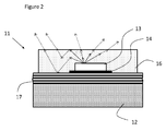
- Figure 2 is a cross-sectional view of an LED device according to the present invention.
- Figure 3 is a plot of reflectance vs wavelength with a zero angle of incidence for four wavelength stacks having center wavelengths spaced 100 nm apart;
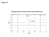
- Figure 4 is a plot of reflectance vs wavelength with a zero angle of incidence for a combined wavelength stack according to a first embodiment of the present invention including four sections having reflectance bandwidths defined by center wavelengths spaced 100 nm apart;
- Figure 5 is a plot of reflectance vs wavelength with a zero angle of incidence for a combined wavelength stack according to a second embodiment of the present invention including approximately fifty high and low index pairs having reflectance bandwidths defined by center wavelengths spaced 10 nm apart;
- Figure 6a is a plot of reflectance vs wavelength for the wavelength stack of the second embodiment at a plurality of different angles of incidence
- Figure 6b is a plot of reflectance vs wavelength for an optimized wavelength stack of the second embodiment at a plurality of different angles of incidence;
- Figure 7 is a plot of average reflectance over a range of 400nm to 680 nm vs angle of incidence comparing metallic reflectors, e.g. silver and aluminum, to the all dielectric reflectors in accordance with the present invention
- Figure 8 is a plot of average reflectance over a range of angles of incidence vs wavelength comparing metallic reflectors, e.g. silver and aluminum, to the all dielectric reflectors in accordance with the present invention
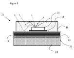
- Figure 9 is a cross-section view of an LED device in accordance with an alternative embodiment of the present invention.
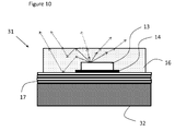
- Figure 10 is a cross-sectional view of an LED device in accordance with an alternative embodiment of the present invention.
- Figure 11 is a plot of average reflectance over a range of 400nm to 680 nm vs angle of incidence comparing metallic reflectors, e.g. silver, to the all dielectric reflector in accordance with the second embodiment of present invention, and the combination of the all dielectric reflector in accordance with the second embodiment of the present invention with an aluminum reflector layer;
- metallic reflectors e.g. silver
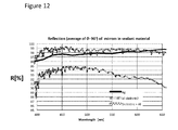
- Figure 12 is a plot of average reflectance over a range of angles of incidence vs wavelength comparing metallic reflectors, e.g. silver, to the all dielectric reflector in accordance with the second embodiment of present invention, and the combination of the all dielectric reflector in accordance with the second embodiment of the present invention with an aluminum reflector layer;
- metallic reflectors e.g. silver
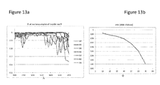
- Figure 13a is a plot of reflectance over a range of angles of incidence vs wavelength
- Figure 13b is a plot of average reflectance vs angle of incidence for the range of wavelengths between 400nm and 700nm.
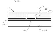
- Figure 14 is a cross-section view of an LED device in accordance with an alternative embodiment of the present invention.
- the present invention relates to a broadband, e. g. white, light emitting diode (LED) device, generally indicated at 11, including a substrate 12, typically formed of silicon or some other semiconductor material, glass (e.g. silica) or in a preferred embodiment, a metallic broadband reflective material, e.g. aluminum.
- a broadband, e.g. white, light emitting diode (LED) device including a substrate 12, typically formed of silicon or some other semiconductor material, glass (e.g. silica) or in a preferred embodiment, a metallic broadband reflective material, e.g. aluminum.
- LED chips 13 e.g. a blue LED made of InGaN
- Electronic circuitry 14 preferably in the form of conductive traces patterned in a conductive oxide layer, e.g. indium tin oxide, is formed around the LED 13 and electrically connected to external power and control sources to provide power and other control and monitoring functions to the LED 13.
- the LED 13 and the electronic circuitry 14 are encapsulated in a transparent sealant material 16, e.g. silicone, which protects the LED 13 and the electronic circuitry 14. Additionally, the sealant material provides insulation and sealing for the electrical contacts and wires making up the electronic circuitry 14. Other types of material can be used, such as epoxy, glass, spin on glass, plastic, polymer, metal or semiconductor material.
- the sealant material 16 includes polymers, which begin in a fluidic state for filling and sealing an interior region around the LED 13. The sealant material 16 is then cured to form a substantially stable state.
- the sealant material 16 is preferably optically transparent or can also be selectively transparent and/or translucent according to specific requirements.
- the sealant material 16, once cured, is substantially inert, and has a low absorption capability to allow a substantial portion of the electromagnetic radiation generated by the LED 11 to traverse therethrough.
- the generation of white light involves passing the light at the initial wavelength, shown as a solid line in Figure 2 , from the LED(s) 11 through a medium including one or more different wavelength conversion materials, e.g. phosphors, creating different wavelengths, e.g. colors, of light, shown as dashed lines in Figure 2 , which combine to form white light.
- wavelength conversion is provided by materials that convert electromagnetic radiation absorbed by the wavelength conversion material.
- the wavelength conversion material 16 is excited by the primary emission of the LED 13 and emits electromagnetic radiation of at least a second wavelength and optionally third and fourth wavelengths, as well.
- the wavelength conversion material is incorporated into the sealant material 16, thereby surrounding and covering the LED 11 on five sides.
- a fraction of the light from the LED 11 undergoes the Stokes shift, and is transformed from shorter wavelengths to longer wavelengths, and if several different phosphor materials of distinct colors are provided within the sealant material 16, the emitted spectrum is broadened even more, preferably to over 150 nm, more preferably over 200 nm, and even more preferably over 250 nm, effectively raising the color rendering index (CRI) value of a given LED.
- CRI color rendering index
- a phosphor-based white LED device 11 includes an encapsulate InGaN blue LED 13 inside a phosphor coated epoxy 16, in which the phosphor is a common yellow phosphor material, such as cerium-doped yttrium aluminum garnet (Ce3+:YAG). Some of the original blue light (420nm-490nm) combines with the transformed yellow light (550nm-600nm) to appear as white light.
- the phosphor is a common yellow phosphor material, such as cerium-doped yttrium aluminum garnet (Ce3+:YAG).
- White LED devices 11 can also be formed using a near-ultraviolet (NUV) LED 11, generating UV light in the 350nm to 400nm range, with a sealant material 16 incorporating a mixture of high-efficiency europium-based phosphors that emit red and blue light, along with copper and aluminum-doped zinc sulfide (ZnS:Cu, Al) that emits green light.
- NUV near-ultraviolet
- ZnS:Cu, Al copper and aluminum-doped zinc sulfide
- the generated red (620nm to 700nm), green (490nm to 570nm) and blue (420nm to 490nm) light combine to form a white light, as is well known in the art.
- the sealant material 16 can be doped or treated with other wavelength adjusting materials to selectively filter, disperse, or influence the original wavelength of light into one or more new wavelengths of light.
- the sealant material 16 can be treated with metals, metal oxides, dielectrics, or semiconductor materials, and/or combinations of these materials to convert the original wavelength to one or more different wavelengths of light with a much wider overall bandwidth, e.g. 150 nm or more, generating white light.
- phosphor particles may be deposited onto the LED 13 or the LED device 11.
- the phosphor particles may comprise any of the wavelength conversion materials listed above, or other materials known in the art.
- the phosphor particles may have a mean-grain-diameter particle size distribution between about 0.1 micron and about 50 microns.
- the particle size distribution of phosphor particles is monomodal, with a peak at an effective diameter between about 0.5 microns and about 40 microns.
- the particle size distribution of phosphor particles is bimodal, with local peaks at two diameters, trimodal, with local peaks at three diameters, or multimodal, with local peaks at four or more effective diameters.
- the entities comprises a phosphor or phosphor blend selected from (Y,Gd,Tb,Sc,Lu,La) 3 (Al,Ga,In) 5 O 12 :Ce 3+ , SrGa 2 S 4 :Eu 2+ , SrS:Eu 2+ , and colloidal quantum dot thin films comprising CdTe, ZnS, ZnSe, ZnTe, CdSe, or CdTe.
- the device may include phosphors capable of emitting substantially red and/or green light. In various embodiments, an amount of phosphor material is selected based on the color balance of the blue LED devices.
- the present invention utilizes a multi-layer dielectric stack 17 of alternating high and low index layers 18 and 19, respectively, designed to provide a broadband reflector, e.g. greater than 150 nm, preferably greater than 200 nm, and more preferably greater than 250 nm, and electrical isolation between the electronic circuitry 14 and the substrate 12.
- the dielectric stack 17 reflects at least 90% of the light in the visible spectrum; however, somewhat smaller bandwidths are within the scope of the invention, e.g. 400 nm to 680 nm (240 nm wide) and 440 nm to 640 nm (200 nm wide).
- the low index layers 19 are comprised of SiO 2
- the high index layers 18 are comprised of one or more of Ta 2 O 5 , Nb 2 O 5 , and TiO 2 ; however, other materials for both the high and low index layers 18 and 19 are within the scope of the invention.
- the dielectric stack 17 is comprised of 4 or 5 sections, each section adapted to reflect light in a predetermined wavelength range, e.g. 75 nm to 125 nm, defined by a center wavelength, which are spaced apart from other center wavelengths by approximately the same distance, e.g. 75 nm to 125 nm, so that there is a small overlap in bandwidth.
- each section is comprised of 8 to 20 layers of alternating high and low index material having a thickness approximately equal to a quarter wavelength of the center wavelength of the predetermined range.
- optical thickness For actual thickness divide the optical thickness by the refractive indices at these wavelengths.
- Figure 3 is a plot of reflectance vs wavelength for a LED device 11 with a silicon substrate 12, but without any sealant material 16, i.e. emitting into the air, at a zero degree angle of incidence.
- the four overlapping reflectance bandwidths for the four aforementioned sections of the dielectric stack 17 defined by the center wavelengths and (not shown) are illustrated.
- Figure 4 is also a plot of reflectance vs wavelength, illustrating the combined broadband reflectance bandwidth for the combined dielectric stack 17, including the plurality of sections as hereinbefore described. Accordingly, the dielectric stack 17 provides 95% to 100% reflectance for a broadband spectrum of light (over 300 nm) emitted into air at a zero degree angle of incidence.
- the dielectric stack 17 can be formed from twenty to fifty different sections, e.g. only one or two pairs of alternating high and low index layers, each pair adapted to reflect a relatively narrow bandwidth, e.g. 10 nm to 25 nm, defined by a center wavelength. Accordingly, the dielectric stack 17 could include quarter wavelength pairs for reflectance bandwidths centered at 350 nm, 360 nm, 370 nm, ... 820 nm, 830 nm, and 840 nm or some smaller subset thereof.
- each layer would be the center wavelength divided by four
- Figure 5 is a plot of wavelength vs reflectance, and illustrates the combined reflectance bandwidth for the aforementioned example for an LED device 11 with a silicon substrate 12, without sealant material 16 at a zero degree angle of incidence.
- the second embodiment provides from 98% to 100% reflectivity for a broadband spectrum of light (over 300 nm from 400 nm to 700 nm) emitted into air at a zero angle of incidence.
- the aforementioned designs are typically optimized using thin film design software.
- Examples of commercially available thin film design software are 'Escential Mcleod', Filmstare, TfCalc, Optilayer.
- the number of layers needed depends on the difference in refractive indices between the high-index and low-index material. The larger the difference the fewer layers are required.
- the total height of the dielectric stack 17 can be in the range of 2 ⁇ m to 20 ⁇ m, preferably 2.5 ⁇ m to 15 ⁇ m, and most preferably between 7 ⁇ m and 12 ⁇ m, providing over 90% reflectivity, preferable over 92.5 % reflectivity, for light from 400 nm to 680 nm at angles of incidence between 0° and 90°.
- the angle of incidence plays a factor in the overall reflectivity of the dielectric stack 17.
- the reflectivity is reduced by 5%, and at a few wavelengths and angles of incidence the reflectivity is reduced by 10% to 15% or more for the aforementioned example of an LED device 11 with a silicon substrate 12, without sealant material 16.
- the spikes can be removed by optimization, as illustrated in Figure 6b , in which the reflectivity reductions at large and small angles of incidence are greatly reduced, providing over 95% reflectivity at all angles and wavelengths between 400 nm and 675 nm.
- the average reflection of the dielectric stack 17 in accordance with either of the aforementioned embodiments, across the visible spectrum (400 nm to 650 nm) and over an angle of incidence range of 0° to 90°, is reduced to approximately 93%, as compared to 97.9% for silver and 91.9% for aluminum.
- an LED device 21, having all of the same elements as the LED device 11, also includes a substrate 22 with a durable metallic reflector layer 23, e.g. comprised of aluminum, between the dielectric stack 17 and the conventional substrate material 24.
- the metallic reflective layer 23 can be as thin as 10 nm to 500 nm, but for practical purposes the reflective layer 23 is typically between 35 nm and 120 nm and ideally between 50 nm and 70 nm, depending upon the thickness requirements of the LED device 21.
- an LED device 31 is illustrated, in which the entire substrate 32 is comprised of a reflective metallic material, ideally aluminum, to provide the additional reflectivity required, as well as to provide increased heat dissipation.
- a material having a thermal conductivity of greater than 100 W/mK, while a material with a thermal conductivity of greater than 200 W/mK, e.g. Al k 250 W/mK, is more preferred. All the other elements, i.e. LED 13, electronic circuitry 14, sealing material 16, and dielectric stack 17 are the same as in Figures 2 and 9 .
- Figure 11 illustrates how the lowest reflectivity for the combined dielectric stack/metallic reflector is over 93%
- Figure 12 illustrates that the average reflectivity of the combined reflector is over 98.5% over the entire visible spectrum, which is greater than either a silver reflector or the dielectric stack 17.
- the thickness of the dielectric stack 17 can be substantially reduced to between 3 ⁇ m and 6 ⁇ m, by reducing the number of layers per section, without sacrificing too much performance in reflectivity.
- the total thickness of the dielectric stack 17 can be in the range of 2 ⁇ m to 20 ⁇ m, preferably 2.5 ⁇ m to 12 ⁇ m, and most preferably between 3 ⁇ m and 8 ⁇ m, providing over 90% reflectivity, preferably over 95 % reflectivity, and most preferably over 97% reflectivity for light having a bandwidth over 250nm, e.g. from 400 nm to 680 nm, at angles of incidence between 0° and 90°.
- the table below provides a comparison of average reflectivities for reflector stacks 17 with different thicknesses.
- the average reflectivity was calculated over an angle range of 0° - 85° and a wavelength range of 400nm to 680nm.
- the above-identified issue with the dielectric stack 17 can be easily addressed by increasing the thickness, effectively 'red shifting' the angular dependence of the coating to longer, less important wavelengths for particular applications.
- the thickness of the dielectric stack 17 should not be increased, as the LED 13 mount on top of the multi-layer dielectric stack 17 needs to dissipate heat therethrough to the substrate, e.g. 4, 12 or 32.
- the substrate e.g. 4, 12 or 32.
- much thicker dielectric stacks 17 provided superior optical performance, but suffered from poor thermal transport across the thin film, effectively making them useless in this application.
- a key feature of an alternative embodiment of an LED device 41 of the present invention is to split up the dielectric stack into at least two areas or segments: a first segment 47a surrounding the LED 13 and electronic circuitry 14 with a first, thicker thickness, e.g. greater than 3.5um, preferably approximately 4 um or more for electrical isolation reasons and the remaining optical performance needed for the omnidirectional mirror comprising the remaining coating.
- Overall coating thickness can be up to 13 um, limited by thermal performance of the structure. The thickness on the overall coating could even be thicker than 13 um, but it would be cost prohibitive.
- a second segment 47b, below the LED 13, is patterned with photolithography or other suitable process, to have a second, thinner thickness to allow the LED 13 to sit a suitable distance from the substrate 12/22/32 so that the electrical isolation is maintained and the thermal impact of the additional thickness of the dielectric stack is minimized, e.g. between 1 um and 3 um, preferably about 2 um.
Landscapes
- Led Device Packages (AREA)
- Optical Filters (AREA)
- Led Devices (AREA)
Applications Claiming Priority (2)
| Application Number | Priority Date | Filing Date | Title |
|---|---|---|---|
| US13/437,742 US9099626B2 (en) | 2012-04-02 | 2012-04-02 | Broadband dielectric reflectors for LED |
| US201261720199P | 2012-10-30 | 2012-10-30 |
Publications (3)
| Publication Number | Publication Date |
|---|---|
| EP2648237A2 true EP2648237A2 (de) | 2013-10-09 |
| EP2648237A3 EP2648237A3 (de) | 2016-01-06 |
| EP2648237B1 EP2648237B1 (de) | 2019-05-15 |
Family
ID=47915519
Family Applications (1)
| Application Number | Title | Priority Date | Filing Date |
|---|---|---|---|
| EP13160439.9A Active EP2648237B1 (de) | 2012-04-02 | 2013-03-21 | Dielektrische Breitband-Reflektoren für Leuchtdioden |
Country Status (5)
| Country | Link |
|---|---|
| EP (1) | EP2648237B1 (de) |
| JP (1) | JP6193596B2 (de) |
| KR (1) | KR102113858B1 (de) |
| CN (1) | CN103367617B (de) |
| TW (1) | TWI575781B (de) |
Cited By (3)
| Publication number | Priority date | Publication date | Assignee | Title |
|---|---|---|---|---|
| CN110383510A (zh) * | 2017-03-08 | 2019-10-25 | 科锐公司 | 用于发光二极管的基板及相关方法 |
| EP4334765A4 (de) * | 2021-05-07 | 2025-08-06 | 3M Innovative Properties Company | Mehrschichtiger optischer film |
| US12471416B2 (en) | 2015-10-23 | 2025-11-11 | Seoul Viosys Co., Ltd. | Light emitting diode chip having distributed bragg reflector |
Families Citing this family (6)
| Publication number | Priority date | Publication date | Assignee | Title |
|---|---|---|---|---|
| JP6398323B2 (ja) | 2014-05-25 | 2018-10-03 | 日亜化学工業株式会社 | 半導体発光素子の製造方法 |
| TW201547059A (zh) * | 2014-06-03 | 2015-12-16 | 邱仕宇 | 發光二極體封裝結構 |
| KR102099386B1 (ko) * | 2014-06-27 | 2020-04-10 | 엘지디스플레이 주식회사 | 백라이트 유닛 및 액정 표시 장치 |
| CN108417569A (zh) * | 2018-05-11 | 2018-08-17 | 深圳市方宇鑫材料科技有限公司 | Led基板及led光源模组 |
| US10683988B2 (en) * | 2018-10-04 | 2020-06-16 | Elemental LED, Inc. | Mirrored LED lighting |
| WO2022011472A1 (en) * | 2020-07-17 | 2022-01-20 | 12180235 Canada Ltd. | Apparatus for reflecting an incident ray of electromagnetic radiation |
Citations (2)
| Publication number | Priority date | Publication date | Assignee | Title |
|---|---|---|---|---|
| US6833565B2 (en) | 2002-12-20 | 2004-12-21 | Industrial Technology Research Institute | White-light led with dielectric omni-directional reflectors |
| US20110186874A1 (en) | 2010-02-03 | 2011-08-04 | Soraa, Inc. | White Light Apparatus and Method |
Family Cites Families (8)
| Publication number | Priority date | Publication date | Assignee | Title |
|---|---|---|---|---|
| KR100576856B1 (ko) | 2003-12-23 | 2006-05-10 | 삼성전기주식회사 | 질화물 반도체 발광소자 및 제조방법 |
| JP2009057551A (ja) * | 2007-08-08 | 2009-03-19 | Mitsubishi Chemicals Corp | 異方性膜用アゾ化合物 |
| JP5634003B2 (ja) * | 2007-09-29 | 2014-12-03 | 日亜化学工業株式会社 | 発光装置 |
| EP2204675B1 (de) | 2007-11-02 | 2016-03-23 | Konica Minolta Opto, Inc. | Optisches element |
| US8017963B2 (en) * | 2008-12-08 | 2011-09-13 | Cree, Inc. | Light emitting diode with a dielectric mirror having a lateral configuration |
| JP5343831B2 (ja) * | 2009-04-16 | 2013-11-13 | 日亜化学工業株式会社 | 発光装置 |
| JP2012033853A (ja) | 2010-04-28 | 2012-02-16 | Fujifilm Corp | 絶縁性光反射基板 |
| JP5725927B2 (ja) * | 2010-05-18 | 2015-05-27 | ソウル バイオシス カンパニー リミテッドSeoul Viosys Co.,Ltd. | 高効率発光ダイオード及びその製造方法 |
-
2013
- 2013-03-21 EP EP13160439.9A patent/EP2648237B1/de active Active
- 2013-03-27 JP JP2013067591A patent/JP6193596B2/ja not_active Expired - Fee Related
- 2013-03-29 KR KR1020130034444A patent/KR102113858B1/ko active Active
- 2013-04-01 TW TW102111730A patent/TWI575781B/zh not_active IP Right Cessation
- 2013-04-02 CN CN201310112923.1A patent/CN103367617B/zh not_active Expired - Fee Related
Patent Citations (2)
| Publication number | Priority date | Publication date | Assignee | Title |
|---|---|---|---|---|
| US6833565B2 (en) | 2002-12-20 | 2004-12-21 | Industrial Technology Research Institute | White-light led with dielectric omni-directional reflectors |
| US20110186874A1 (en) | 2010-02-03 | 2011-08-04 | Soraa, Inc. | White Light Apparatus and Method |
Cited By (4)
| Publication number | Priority date | Publication date | Assignee | Title |
|---|---|---|---|---|
| US12471416B2 (en) | 2015-10-23 | 2025-11-11 | Seoul Viosys Co., Ltd. | Light emitting diode chip having distributed bragg reflector |
| CN110383510A (zh) * | 2017-03-08 | 2019-10-25 | 科锐公司 | 用于发光二极管的基板及相关方法 |
| CN110383510B (zh) * | 2017-03-08 | 2024-02-06 | 科锐Led公司 | 用于发光二极管的基板及相关方法 |
| EP4334765A4 (de) * | 2021-05-07 | 2025-08-06 | 3M Innovative Properties Company | Mehrschichtiger optischer film |
Also Published As
| Publication number | Publication date |
|---|---|
| JP6193596B2 (ja) | 2017-09-06 |
| TWI575781B (zh) | 2017-03-21 |
| CN103367617A (zh) | 2013-10-23 |
| KR102113858B1 (ko) | 2020-05-21 |
| TW201347243A (zh) | 2013-11-16 |
| EP2648237A3 (de) | 2016-01-06 |
| CN103367617B (zh) | 2018-03-09 |
| JP2013214742A (ja) | 2013-10-17 |
| EP2648237B1 (de) | 2019-05-15 |
| KR20130111996A (ko) | 2013-10-11 |
Similar Documents
| Publication | Publication Date | Title |
|---|---|---|
| EP2648237B1 (de) | Dielektrische Breitband-Reflektoren für Leuchtdioden | |
| US8889517B2 (en) | Broadband dielectric reflectors for LED with varying thickness | |
| US9099626B2 (en) | Broadband dielectric reflectors for LED | |
| JP6674978B2 (ja) | 発光ダイオードパッケージ | |
| EP2374165B1 (de) | Leuchtdiodenanordnung | |
| CN107689413B (zh) | 发光装置和发光装置的制造方法 | |
| US11043615B2 (en) | Light-emitting device having a dielectric multilayer film arranged on the side surface of the light-emitting element | |
| US9518718B2 (en) | Bandpass filter for use in light emitting device and light emitting device using the same | |
| US8410504B2 (en) | LED module | |
| CN101081980A (zh) | 波长变换构件和发光装置 | |
| EP3830216B1 (de) | Reflektive farbkorrektur für leuchtstoffbeleuchtungssysteme | |
| JP2013501374A (ja) | 誘電体コーティングを用いる高出力led装置アーキテクチャおよび製造方法 | |
| US20230110159A1 (en) | Light emitting device and method of fabricating thereof | |
| CN110350066B (zh) | 具有反射结构的光转换材料与应用其的发光二极管元件 | |
| US20250362438A1 (en) | Long-pass filter structures for light-emitting diodes |
Legal Events
| Date | Code | Title | Description |
|---|---|---|---|
| PUAI | Public reference made under article 153(3) epc to a published international application that has entered the european phase |
Free format text: ORIGINAL CODE: 0009012 |
|
| AK | Designated contracting states |
Kind code of ref document: A2 Designated state(s): AL AT BE BG CH CY CZ DE DK EE ES FI FR GB GR HR HU IE IS IT LI LT LU LV MC MK MT NL NO PL PT RO RS SE SI SK SM TR |
|
| AX | Request for extension of the european patent |
Extension state: BA ME |
|
| PUAL | Search report despatched |
Free format text: ORIGINAL CODE: 0009013 |
|
| RAP1 | Party data changed (applicant data changed or rights of an application transferred) |
Owner name: VIAVI SOLUTIONS INC. |
|
| AK | Designated contracting states |
Kind code of ref document: A3 Designated state(s): AL AT BE BG CH CY CZ DE DK EE ES FI FR GB GR HR HU IE IS IT LI LT LU LV MC MK MT NL NO PL PT RO RS SE SI SK SM TR |
|
| AX | Request for extension of the european patent |
Extension state: BA ME |
|
| RIC1 | Information provided on ipc code assigned before grant |
Ipc: H01L 33/46 20100101AFI20151201BHEP |
|
| 17P | Request for examination filed |
Effective date: 20160704 |
|
| RBV | Designated contracting states (corrected) |
Designated state(s): AL AT BE BG CH CY CZ DE DK EE ES FI FR GB GR HR HU IE IS IT LI LT LU LV MC MK MT NL NO PL PT RO RS SE SI SK SM TR |
|
| RAP1 | Party data changed (applicant data changed or rights of an application transferred) |
Owner name: VIAVI SOLUTIONS INC. |
|
| GRAP | Despatch of communication of intention to grant a patent |
Free format text: ORIGINAL CODE: EPIDOSNIGR1 |
|
| STAA | Information on the status of an ep patent application or granted ep patent |
Free format text: STATUS: GRANT OF PATENT IS INTENDED |
|
| RIC1 | Information provided on ipc code assigned before grant |
Ipc: H01L 33/60 20100101ALN20181113BHEP Ipc: H01L 33/46 20100101AFI20181113BHEP Ipc: H01L 33/64 20100101ALN20181113BHEP |
|
| RIC1 | Information provided on ipc code assigned before grant |
Ipc: H01L 33/46 20100101AFI20181121BHEP Ipc: H01L 33/64 20100101ALN20181121BHEP Ipc: H01L 33/60 20100101ALN20181121BHEP |
|
| INTG | Intention to grant announced |
Effective date: 20181205 |
|
| GRAS | Grant fee paid |
Free format text: ORIGINAL CODE: EPIDOSNIGR3 |
|
| GRAA | (expected) grant |
Free format text: ORIGINAL CODE: 0009210 |
|
| STAA | Information on the status of an ep patent application or granted ep patent |
Free format text: STATUS: THE PATENT HAS BEEN GRANTED |
|
| AK | Designated contracting states |
Kind code of ref document: B1 Designated state(s): AL AT BE BG CH CY CZ DE DK EE ES FI FR GB GR HR HU IE IS IT LI LT LU LV MC MK MT NL NO PL PT RO RS SE SI SK SM TR |
|
| REG | Reference to a national code |
Ref country code: CH Ref legal event code: EP Ref country code: GB Ref legal event code: FG4D |
|
| REG | Reference to a national code |
Ref country code: DE Ref legal event code: R096 Ref document number: 602013055327 Country of ref document: DE |
|
| REG | Reference to a national code |
Ref country code: IE Ref legal event code: FG4D |
|
| REG | Reference to a national code |
Ref country code: CH Ref legal event code: NV Representative=s name: MURGITROYD AND COMPANY, CH |
|
| REG | Reference to a national code |
Ref country code: NL Ref legal event code: MP Effective date: 20190515 |
|
| REG | Reference to a national code |
Ref country code: LT Ref legal event code: MG4D |
|
| PG25 | Lapsed in a contracting state [announced via postgrant information from national office to epo] |
Ref country code: FI Free format text: LAPSE BECAUSE OF FAILURE TO SUBMIT A TRANSLATION OF THE DESCRIPTION OR TO PAY THE FEE WITHIN THE PRESCRIBED TIME-LIMIT Effective date: 20190515 Ref country code: AL Free format text: LAPSE BECAUSE OF FAILURE TO SUBMIT A TRANSLATION OF THE DESCRIPTION OR TO PAY THE FEE WITHIN THE PRESCRIBED TIME-LIMIT Effective date: 20190515 Ref country code: PT Free format text: LAPSE BECAUSE OF FAILURE TO SUBMIT A TRANSLATION OF THE DESCRIPTION OR TO PAY THE FEE WITHIN THE PRESCRIBED TIME-LIMIT Effective date: 20190915 Ref country code: NO Free format text: LAPSE BECAUSE OF FAILURE TO SUBMIT A TRANSLATION OF THE DESCRIPTION OR TO PAY THE FEE WITHIN THE PRESCRIBED TIME-LIMIT Effective date: 20190815 Ref country code: HR Free format text: LAPSE BECAUSE OF FAILURE TO SUBMIT A TRANSLATION OF THE DESCRIPTION OR TO PAY THE FEE WITHIN THE PRESCRIBED TIME-LIMIT Effective date: 20190515 Ref country code: NL Free format text: LAPSE BECAUSE OF FAILURE TO SUBMIT A TRANSLATION OF THE DESCRIPTION OR TO PAY THE FEE WITHIN THE PRESCRIBED TIME-LIMIT Effective date: 20190515 Ref country code: SE Free format text: LAPSE BECAUSE OF FAILURE TO SUBMIT A TRANSLATION OF THE DESCRIPTION OR TO PAY THE FEE WITHIN THE PRESCRIBED TIME-LIMIT Effective date: 20190515 Ref country code: LT Free format text: LAPSE BECAUSE OF FAILURE TO SUBMIT A TRANSLATION OF THE DESCRIPTION OR TO PAY THE FEE WITHIN THE PRESCRIBED TIME-LIMIT Effective date: 20190515 Ref country code: ES Free format text: LAPSE BECAUSE OF FAILURE TO SUBMIT A TRANSLATION OF THE DESCRIPTION OR TO PAY THE FEE WITHIN THE PRESCRIBED TIME-LIMIT Effective date: 20190515 |
|
| PG25 | Lapsed in a contracting state [announced via postgrant information from national office to epo] |
Ref country code: LV Free format text: LAPSE BECAUSE OF FAILURE TO SUBMIT A TRANSLATION OF THE DESCRIPTION OR TO PAY THE FEE WITHIN THE PRESCRIBED TIME-LIMIT Effective date: 20190515 Ref country code: RS Free format text: LAPSE BECAUSE OF FAILURE TO SUBMIT A TRANSLATION OF THE DESCRIPTION OR TO PAY THE FEE WITHIN THE PRESCRIBED TIME-LIMIT Effective date: 20190515 Ref country code: BG Free format text: LAPSE BECAUSE OF FAILURE TO SUBMIT A TRANSLATION OF THE DESCRIPTION OR TO PAY THE FEE WITHIN THE PRESCRIBED TIME-LIMIT Effective date: 20190815 Ref country code: GR Free format text: LAPSE BECAUSE OF FAILURE TO SUBMIT A TRANSLATION OF THE DESCRIPTION OR TO PAY THE FEE WITHIN THE PRESCRIBED TIME-LIMIT Effective date: 20190816 |
|
| REG | Reference to a national code |
Ref country code: AT Ref legal event code: MK05 Ref document number: 1134452 Country of ref document: AT Kind code of ref document: T Effective date: 20190515 |
|
| PG25 | Lapsed in a contracting state [announced via postgrant information from national office to epo] |
Ref country code: CZ Free format text: LAPSE BECAUSE OF FAILURE TO SUBMIT A TRANSLATION OF THE DESCRIPTION OR TO PAY THE FEE WITHIN THE PRESCRIBED TIME-LIMIT Effective date: 20190515 Ref country code: SK Free format text: LAPSE BECAUSE OF FAILURE TO SUBMIT A TRANSLATION OF THE DESCRIPTION OR TO PAY THE FEE WITHIN THE PRESCRIBED TIME-LIMIT Effective date: 20190515 Ref country code: DK Free format text: LAPSE BECAUSE OF FAILURE TO SUBMIT A TRANSLATION OF THE DESCRIPTION OR TO PAY THE FEE WITHIN THE PRESCRIBED TIME-LIMIT Effective date: 20190515 Ref country code: AT Free format text: LAPSE BECAUSE OF FAILURE TO SUBMIT A TRANSLATION OF THE DESCRIPTION OR TO PAY THE FEE WITHIN THE PRESCRIBED TIME-LIMIT Effective date: 20190515 Ref country code: EE Free format text: LAPSE BECAUSE OF FAILURE TO SUBMIT A TRANSLATION OF THE DESCRIPTION OR TO PAY THE FEE WITHIN THE PRESCRIBED TIME-LIMIT Effective date: 20190515 Ref country code: RO Free format text: LAPSE BECAUSE OF FAILURE TO SUBMIT A TRANSLATION OF THE DESCRIPTION OR TO PAY THE FEE WITHIN THE PRESCRIBED TIME-LIMIT Effective date: 20190515 |
|
| REG | Reference to a national code |
Ref country code: DE Ref legal event code: R097 Ref document number: 602013055327 Country of ref document: DE |
|
| PG25 | Lapsed in a contracting state [announced via postgrant information from national office to epo] |
Ref country code: IT Free format text: LAPSE BECAUSE OF FAILURE TO SUBMIT A TRANSLATION OF THE DESCRIPTION OR TO PAY THE FEE WITHIN THE PRESCRIBED TIME-LIMIT Effective date: 20190515 Ref country code: SM Free format text: LAPSE BECAUSE OF FAILURE TO SUBMIT A TRANSLATION OF THE DESCRIPTION OR TO PAY THE FEE WITHIN THE PRESCRIBED TIME-LIMIT Effective date: 20190515 |
|
| PLBE | No opposition filed within time limit |
Free format text: ORIGINAL CODE: 0009261 |
|
| STAA | Information on the status of an ep patent application or granted ep patent |
Free format text: STATUS: NO OPPOSITION FILED WITHIN TIME LIMIT |
|
| PG25 | Lapsed in a contracting state [announced via postgrant information from national office to epo] |
Ref country code: TR Free format text: LAPSE BECAUSE OF FAILURE TO SUBMIT A TRANSLATION OF THE DESCRIPTION OR TO PAY THE FEE WITHIN THE PRESCRIBED TIME-LIMIT Effective date: 20190515 |
|
| 26N | No opposition filed |
Effective date: 20200218 |
|
| PG25 | Lapsed in a contracting state [announced via postgrant information from national office to epo] |
Ref country code: PL Free format text: LAPSE BECAUSE OF FAILURE TO SUBMIT A TRANSLATION OF THE DESCRIPTION OR TO PAY THE FEE WITHIN THE PRESCRIBED TIME-LIMIT Effective date: 20190515 |
|
| PGFP | Annual fee paid to national office [announced via postgrant information from national office to epo] |
Ref country code: DE Payment date: 20200326 Year of fee payment: 8 Ref country code: GB Payment date: 20200330 Year of fee payment: 8 |
|
| PG25 | Lapsed in a contracting state [announced via postgrant information from national office to epo] |
Ref country code: SI Free format text: LAPSE BECAUSE OF FAILURE TO SUBMIT A TRANSLATION OF THE DESCRIPTION OR TO PAY THE FEE WITHIN THE PRESCRIBED TIME-LIMIT Effective date: 20190515 |
|
| PGFP | Annual fee paid to national office [announced via postgrant information from national office to epo] |
Ref country code: CH Payment date: 20200327 Year of fee payment: 8 |
|
| PGFP | Annual fee paid to national office [announced via postgrant information from national office to epo] |
Ref country code: FR Payment date: 20200326 Year of fee payment: 8 Ref country code: MT Payment date: 20200228 Year of fee payment: 8 |
|
| PG25 | Lapsed in a contracting state [announced via postgrant information from national office to epo] |
Ref country code: MC Free format text: LAPSE BECAUSE OF FAILURE TO SUBMIT A TRANSLATION OF THE DESCRIPTION OR TO PAY THE FEE WITHIN THE PRESCRIBED TIME-LIMIT Effective date: 20190515 |
|
| REG | Reference to a national code |
Ref country code: BE Ref legal event code: MM Effective date: 20200331 |
|
| PG25 | Lapsed in a contracting state [announced via postgrant information from national office to epo] |
Ref country code: LU Free format text: LAPSE BECAUSE OF NON-PAYMENT OF DUE FEES Effective date: 20200321 |
|
| PG25 | Lapsed in a contracting state [announced via postgrant information from national office to epo] |
Ref country code: IE Free format text: LAPSE BECAUSE OF NON-PAYMENT OF DUE FEES Effective date: 20200321 |
|
| PG25 | Lapsed in a contracting state [announced via postgrant information from national office to epo] |
Ref country code: BE Free format text: LAPSE BECAUSE OF NON-PAYMENT OF DUE FEES Effective date: 20200331 |
|
| REG | Reference to a national code |
Ref country code: DE Ref legal event code: R119 Ref document number: 602013055327 Country of ref document: DE |
|
| REG | Reference to a national code |
Ref country code: CH Ref legal event code: PL |
|
| GBPC | Gb: european patent ceased through non-payment of renewal fee |
Effective date: 20210321 |
|
| PG25 | Lapsed in a contracting state [announced via postgrant information from national office to epo] |
Ref country code: DE Free format text: LAPSE BECAUSE OF NON-PAYMENT OF DUE FEES Effective date: 20211001 Ref country code: FR Free format text: LAPSE BECAUSE OF NON-PAYMENT OF DUE FEES Effective date: 20210331 Ref country code: GB Free format text: LAPSE BECAUSE OF NON-PAYMENT OF DUE FEES Effective date: 20210321 Ref country code: LI Free format text: LAPSE BECAUSE OF NON-PAYMENT OF DUE FEES Effective date: 20210331 Ref country code: CH Free format text: LAPSE BECAUSE OF NON-PAYMENT OF DUE FEES Effective date: 20210331 |
|
| PG25 | Lapsed in a contracting state [announced via postgrant information from national office to epo] |
Ref country code: CY Free format text: LAPSE BECAUSE OF FAILURE TO SUBMIT A TRANSLATION OF THE DESCRIPTION OR TO PAY THE FEE WITHIN THE PRESCRIBED TIME-LIMIT Effective date: 20190515 |
|
| PG25 | Lapsed in a contracting state [announced via postgrant information from national office to epo] |
Ref country code: MT Free format text: LAPSE BECAUSE OF NON-PAYMENT OF DUE FEES Effective date: 20210321 Ref country code: MK Free format text: LAPSE BECAUSE OF FAILURE TO SUBMIT A TRANSLATION OF THE DESCRIPTION OR TO PAY THE FEE WITHIN THE PRESCRIBED TIME-LIMIT Effective date: 20190515 Ref country code: IS Free format text: LAPSE BECAUSE OF FAILURE TO SUBMIT A TRANSLATION OF THE DESCRIPTION OR TO PAY THE FEE WITHIN THE PRESCRIBED TIME-LIMIT Effective date: 20190915 |
|
| P01 | Opt-out of the competence of the unified patent court (upc) registered |
Effective date: 20230530 |