EP2641267B1 - Semiconductor wafer comprising gallium nitride layer having one or more silicon nitride interlayer therein - Google Patents
Semiconductor wafer comprising gallium nitride layer having one or more silicon nitride interlayer therein Download PDFInfo
- Publication number
- EP2641267B1 EP2641267B1 EP11773114.1A EP11773114A EP2641267B1 EP 2641267 B1 EP2641267 B1 EP 2641267B1 EP 11773114 A EP11773114 A EP 11773114A EP 2641267 B1 EP2641267 B1 EP 2641267B1
- Authority
- EP
- European Patent Office
- Prior art keywords
- layer
- gan
- interlayer
- thickness
- semiconductor wafer
- Prior art date
- Legal status (The legal status is an assumption and is not a legal conclusion. Google has not performed a legal analysis and makes no representation as to the accuracy of the status listed.)
- Active
Links
Images

Classifications
-
- H—ELECTRICITY
- H10—SEMICONDUCTOR DEVICES; ELECTRIC SOLID-STATE DEVICES NOT OTHERWISE PROVIDED FOR
- H10H—INORGANIC LIGHT-EMITTING SEMICONDUCTOR DEVICES HAVING POTENTIAL BARRIERS
- H10H20/00—Individual inorganic light-emitting semiconductor devices having potential barriers, e.g. light-emitting diodes [LED]
- H10H20/80—Constructional details
- H10H20/81—Bodies
- H10H20/822—Materials of the light-emitting regions
- H10H20/824—Materials of the light-emitting regions comprising only Group III-V materials, e.g. GaP
- H10H20/825—Materials of the light-emitting regions comprising only Group III-V materials, e.g. GaP containing nitrogen, e.g. GaN
-
- H—ELECTRICITY
- H10—SEMICONDUCTOR DEVICES; ELECTRIC SOLID-STATE DEVICES NOT OTHERWISE PROVIDED FOR
- H10P—GENERIC PROCESSES OR APPARATUS FOR THE MANUFACTURE OR TREATMENT OF DEVICES COVERED BY CLASS H10
- H10P14/00—Formation of materials, e.g. in the shape of layers or pillars
- H10P14/20—Formation of materials, e.g. in the shape of layers or pillars of semiconductor materials
- H10P14/29—Formation of materials, e.g. in the shape of layers or pillars of semiconductor materials characterised by the substrates
-
- B—PERFORMING OPERATIONS; TRANSPORTING
- B82—NANOTECHNOLOGY
- B82Y—SPECIFIC USES OR APPLICATIONS OF NANOSTRUCTURES; MEASUREMENT OR ANALYSIS OF NANOSTRUCTURES; MANUFACTURE OR TREATMENT OF NANOSTRUCTURES
- B82Y20/00—Nanooptics, e.g. quantum optics or photonic crystals
-
- H—ELECTRICITY
- H10—SEMICONDUCTOR DEVICES; ELECTRIC SOLID-STATE DEVICES NOT OTHERWISE PROVIDED FOR
- H10F—INORGANIC SEMICONDUCTOR DEVICES SENSITIVE TO INFRARED RADIATION, LIGHT, ELECTROMAGNETIC RADIATION OF SHORTER WAVELENGTH OR CORPUSCULAR RADIATION
- H10F10/00—Individual photovoltaic cells, e.g. solar cells
- H10F10/10—Individual photovoltaic cells, e.g. solar cells having potential barriers
- H10F10/17—Photovoltaic cells having only PIN junction potential barriers
-
- H—ELECTRICITY
- H10—SEMICONDUCTOR DEVICES; ELECTRIC SOLID-STATE DEVICES NOT OTHERWISE PROVIDED FOR
- H10F—INORGANIC SEMICONDUCTOR DEVICES SENSITIVE TO INFRARED RADIATION, LIGHT, ELECTROMAGNETIC RADIATION OF SHORTER WAVELENGTH OR CORPUSCULAR RADIATION
- H10F71/00—Manufacture or treatment of devices covered by this subclass
- H10F71/127—The active layers comprising only Group III-V materials, e.g. GaAs or InP
- H10F71/1276—The active layers comprising only Group III-V materials, e.g. GaAs or InP comprising growth substrates not made of Group III-V materials
-
- H—ELECTRICITY
- H10—SEMICONDUCTOR DEVICES; ELECTRIC SOLID-STATE DEVICES NOT OTHERWISE PROVIDED FOR
- H10F—INORGANIC SEMICONDUCTOR DEVICES SENSITIVE TO INFRARED RADIATION, LIGHT, ELECTROMAGNETIC RADIATION OF SHORTER WAVELENGTH OR CORPUSCULAR RADIATION
- H10F71/00—Manufacture or treatment of devices covered by this subclass
- H10F71/127—The active layers comprising only Group III-V materials, e.g. GaAs or InP
- H10F71/1278—The active layers comprising only Group III-V materials, e.g. GaAs or InP comprising nitrides, e.g. GaN
-
- H—ELECTRICITY
- H10—SEMICONDUCTOR DEVICES; ELECTRIC SOLID-STATE DEVICES NOT OTHERWISE PROVIDED FOR
- H10F—INORGANIC SEMICONDUCTOR DEVICES SENSITIVE TO INFRARED RADIATION, LIGHT, ELECTROMAGNETIC RADIATION OF SHORTER WAVELENGTH OR CORPUSCULAR RADIATION
- H10F77/00—Constructional details of devices covered by this subclass
- H10F77/10—Semiconductor bodies
- H10F77/12—Active materials
- H10F77/124—Active materials comprising only Group III-V materials, e.g. GaAs
- H10F77/1248—Active materials comprising only Group III-V materials, e.g. GaAs having three or more elements, e.g. GaAlAs, InGaAs or InGaAsP
- H10F77/12485—Active materials comprising only Group III-V materials, e.g. GaAs having three or more elements, e.g. GaAlAs, InGaAs or InGaAsP comprising nitride compounds, e.g. InGaN
-
- H—ELECTRICITY
- H10—SEMICONDUCTOR DEVICES; ELECTRIC SOLID-STATE DEVICES NOT OTHERWISE PROVIDED FOR
- H10F—INORGANIC SEMICONDUCTOR DEVICES SENSITIVE TO INFRARED RADIATION, LIGHT, ELECTROMAGNETIC RADIATION OF SHORTER WAVELENGTH OR CORPUSCULAR RADIATION
- H10F77/00—Constructional details of devices covered by this subclass
- H10F77/10—Semiconductor bodies
- H10F77/14—Shape of semiconductor bodies; Shapes, relative sizes or dispositions of semiconductor regions within semiconductor bodies
- H10F77/146—Superlattices; Multiple quantum well structures
-
- H—ELECTRICITY
- H10—SEMICONDUCTOR DEVICES; ELECTRIC SOLID-STATE DEVICES NOT OTHERWISE PROVIDED FOR
- H10P—GENERIC PROCESSES OR APPARATUS FOR THE MANUFACTURE OR TREATMENT OF DEVICES COVERED BY CLASS H10
- H10P14/00—Formation of materials, e.g. in the shape of layers or pillars
- H10P14/20—Formation of materials, e.g. in the shape of layers or pillars of semiconductor materials
- H10P14/24—Formation of materials, e.g. in the shape of layers or pillars of semiconductor materials using chemical vapour deposition [CVD]
-
- H—ELECTRICITY
- H10—SEMICONDUCTOR DEVICES; ELECTRIC SOLID-STATE DEVICES NOT OTHERWISE PROVIDED FOR
- H10P—GENERIC PROCESSES OR APPARATUS FOR THE MANUFACTURE OR TREATMENT OF DEVICES COVERED BY CLASS H10
- H10P14/00—Formation of materials, e.g. in the shape of layers or pillars
- H10P14/20—Formation of materials, e.g. in the shape of layers or pillars of semiconductor materials
- H10P14/29—Formation of materials, e.g. in the shape of layers or pillars of semiconductor materials characterised by the substrates
- H10P14/2901—Materials
- H10P14/2902—Materials being Group IVA materials
- H10P14/2905—Silicon, silicon germanium or germanium
-
- H—ELECTRICITY
- H10—SEMICONDUCTOR DEVICES; ELECTRIC SOLID-STATE DEVICES NOT OTHERWISE PROVIDED FOR
- H10P—GENERIC PROCESSES OR APPARATUS FOR THE MANUFACTURE OR TREATMENT OF DEVICES COVERED BY CLASS H10
- H10P14/00—Formation of materials, e.g. in the shape of layers or pillars
- H10P14/20—Formation of materials, e.g. in the shape of layers or pillars of semiconductor materials
- H10P14/29—Formation of materials, e.g. in the shape of layers or pillars of semiconductor materials characterised by the substrates
- H10P14/2901—Materials
- H10P14/2921—Materials being crystalline insulating materials
-
- H—ELECTRICITY
- H10—SEMICONDUCTOR DEVICES; ELECTRIC SOLID-STATE DEVICES NOT OTHERWISE PROVIDED FOR
- H10P—GENERIC PROCESSES OR APPARATUS FOR THE MANUFACTURE OR TREATMENT OF DEVICES COVERED BY CLASS H10
- H10P14/00—Formation of materials, e.g. in the shape of layers or pillars
- H10P14/20—Formation of materials, e.g. in the shape of layers or pillars of semiconductor materials
- H10P14/32—Formation of materials, e.g. in the shape of layers or pillars of semiconductor materials characterised by intermediate layers between substrates and deposited layers
- H10P14/3202—Materials thereof
- H10P14/3214—Materials thereof being Group IIIA-VA semiconductors
- H10P14/3216—Nitrides
-
- H—ELECTRICITY
- H10—SEMICONDUCTOR DEVICES; ELECTRIC SOLID-STATE DEVICES NOT OTHERWISE PROVIDED FOR
- H10P—GENERIC PROCESSES OR APPARATUS FOR THE MANUFACTURE OR TREATMENT OF DEVICES COVERED BY CLASS H10
- H10P14/00—Formation of materials, e.g. in the shape of layers or pillars
- H10P14/20—Formation of materials, e.g. in the shape of layers or pillars of semiconductor materials
- H10P14/32—Formation of materials, e.g. in the shape of layers or pillars of semiconductor materials characterised by intermediate layers between substrates and deposited layers
- H10P14/3202—Materials thereof
- H10P14/3238—Materials thereof being insulating materials
-
- H—ELECTRICITY
- H10—SEMICONDUCTOR DEVICES; ELECTRIC SOLID-STATE DEVICES NOT OTHERWISE PROVIDED FOR
- H10P—GENERIC PROCESSES OR APPARATUS FOR THE MANUFACTURE OR TREATMENT OF DEVICES COVERED BY CLASS H10
- H10P14/00—Formation of materials, e.g. in the shape of layers or pillars
- H10P14/20—Formation of materials, e.g. in the shape of layers or pillars of semiconductor materials
- H10P14/32—Formation of materials, e.g. in the shape of layers or pillars of semiconductor materials characterised by intermediate layers between substrates and deposited layers
- H10P14/3242—Structure
- H10P14/3244—Layer structure
- H10P14/3251—Layer structure consisting of three or more layers
-
- H—ELECTRICITY
- H10—SEMICONDUCTOR DEVICES; ELECTRIC SOLID-STATE DEVICES NOT OTHERWISE PROVIDED FOR
- H10P—GENERIC PROCESSES OR APPARATUS FOR THE MANUFACTURE OR TREATMENT OF DEVICES COVERED BY CLASS H10
- H10P14/00—Formation of materials, e.g. in the shape of layers or pillars
- H10P14/20—Formation of materials, e.g. in the shape of layers or pillars of semiconductor materials
- H10P14/32—Formation of materials, e.g. in the shape of layers or pillars of semiconductor materials characterised by intermediate layers between substrates and deposited layers
- H10P14/3242—Structure
- H10P14/3244—Layer structure
- H10P14/3254—Graded layers
-
- H—ELECTRICITY
- H10—SEMICONDUCTOR DEVICES; ELECTRIC SOLID-STATE DEVICES NOT OTHERWISE PROVIDED FOR
- H10P—GENERIC PROCESSES OR APPARATUS FOR THE MANUFACTURE OR TREATMENT OF DEVICES COVERED BY CLASS H10
- H10P14/00—Formation of materials, e.g. in the shape of layers or pillars
- H10P14/20—Formation of materials, e.g. in the shape of layers or pillars of semiconductor materials
- H10P14/34—Deposited materials, e.g. layers
- H10P14/3402—Deposited materials, e.g. layers characterised by the chemical composition
- H10P14/3414—Deposited materials, e.g. layers characterised by the chemical composition being group IIIA-VIA materials
- H10P14/3416—Nitrides
-
- H—ELECTRICITY
- H10—SEMICONDUCTOR DEVICES; ELECTRIC SOLID-STATE DEVICES NOT OTHERWISE PROVIDED FOR
- H10P—GENERIC PROCESSES OR APPARATUS FOR THE MANUFACTURE OR TREATMENT OF DEVICES COVERED BY CLASS H10
- H10P14/00—Formation of materials, e.g. in the shape of layers or pillars
- H10P14/20—Formation of materials, e.g. in the shape of layers or pillars of semiconductor materials
- H10P14/34—Deposited materials, e.g. layers
- H10P14/3438—Doping during depositing
- H10P14/3441—Conductivity type
-
- H—ELECTRICITY
- H10—SEMICONDUCTOR DEVICES; ELECTRIC SOLID-STATE DEVICES NOT OTHERWISE PROVIDED FOR
- H10H—INORGANIC LIGHT-EMITTING SEMICONDUCTOR DEVICES HAVING POTENTIAL BARRIERS
- H10H20/00—Individual inorganic light-emitting semiconductor devices having potential barriers, e.g. light-emitting diodes [LED]
- H10H20/01—Manufacture or treatment
- H10H20/011—Manufacture or treatment of bodies, e.g. forming semiconductor layers
- H10H20/013—Manufacture or treatment of bodies, e.g. forming semiconductor layers having light-emitting regions comprising only Group III-V materials
- H10H20/0133—Manufacture or treatment of bodies, e.g. forming semiconductor layers having light-emitting regions comprising only Group III-V materials with a substrate not being Group III-V materials
- H10H20/01335—Manufacture or treatment of bodies, e.g. forming semiconductor layers having light-emitting regions comprising only Group III-V materials with a substrate not being Group III-V materials the light-emitting regions comprising nitride materials
-
- H—ELECTRICITY
- H10—SEMICONDUCTOR DEVICES; ELECTRIC SOLID-STATE DEVICES NOT OTHERWISE PROVIDED FOR
- H10H—INORGANIC LIGHT-EMITTING SEMICONDUCTOR DEVICES HAVING POTENTIAL BARRIERS
- H10H20/00—Individual inorganic light-emitting semiconductor devices having potential barriers, e.g. light-emitting diodes [LED]
- H10H20/80—Constructional details
- H10H20/81—Bodies
- H10H20/815—Bodies having stress relaxation structures, e.g. buffer layers
-
- H—ELECTRICITY
- H10—SEMICONDUCTOR DEVICES; ELECTRIC SOLID-STATE DEVICES NOT OTHERWISE PROVIDED FOR
- H10P—GENERIC PROCESSES OR APPARATUS FOR THE MANUFACTURE OR TREATMENT OF DEVICES COVERED BY CLASS H10
- H10P14/00—Formation of materials, e.g. in the shape of layers or pillars
- H10P14/20—Formation of materials, e.g. in the shape of layers or pillars of semiconductor materials
- H10P14/29—Formation of materials, e.g. in the shape of layers or pillars of semiconductor materials characterised by the substrates
- H10P14/2901—Materials
- H10P14/2907—Materials being Group IIIA-VA materials
- H10P14/2908—Nitrides
-
- Y—GENERAL TAGGING OF NEW TECHNOLOGICAL DEVELOPMENTS; GENERAL TAGGING OF CROSS-SECTIONAL TECHNOLOGIES SPANNING OVER SEVERAL SECTIONS OF THE IPC; TECHNICAL SUBJECTS COVERED BY FORMER USPC CROSS-REFERENCE ART COLLECTIONS [XRACs] AND DIGESTS
- Y02—TECHNOLOGIES OR APPLICATIONS FOR MITIGATION OR ADAPTATION AGAINST CLIMATE CHANGE
- Y02E—REDUCTION OF GREENHOUSE GAS [GHG] EMISSIONS, RELATED TO ENERGY GENERATION, TRANSMISSION OR DISTRIBUTION
- Y02E10/00—Energy generation through renewable energy sources
- Y02E10/50—Photovoltaic [PV] energy
- Y02E10/544—Solar cells from Group III-V materials
-
- Y—GENERAL TAGGING OF NEW TECHNOLOGICAL DEVELOPMENTS; GENERAL TAGGING OF CROSS-SECTIONAL TECHNOLOGIES SPANNING OVER SEVERAL SECTIONS OF THE IPC; TECHNICAL SUBJECTS COVERED BY FORMER USPC CROSS-REFERENCE ART COLLECTIONS [XRACs] AND DIGESTS
- Y02—TECHNOLOGIES OR APPLICATIONS FOR MITIGATION OR ADAPTATION AGAINST CLIMATE CHANGE
- Y02E—REDUCTION OF GREENHOUSE GAS [GHG] EMISSIONS, RELATED TO ENERGY GENERATION, TRANSMISSION OR DISTRIBUTION
- Y02E10/00—Energy generation through renewable energy sources
- Y02E10/50—Photovoltaic [PV] energy
- Y02E10/548—Amorphous silicon PV cells
Definitions
- the present invention relates to a semiconductor material and the use of a semiconductor material in wafer-form for forming a light emitting diode (LED) or other optoelectronic device. Further, the present invention relates to a method of constructing high quality optoelectronic devices using the wafer. In particular, the present invention relates to an improved LED having a silicon substrate that minimises the dislocation-defects and wafer bow/cracking when large support wafers are used.
- Optoelectronic devices are well known and it is also known that for such devices it is desirable to minimise the occurrence of defects in the semiconductor layers that form part of the structure of the device.
- Common defects in LEDs include threading (edge or screw type) dislocations which lead to a reduced luminescent efficiency in the final product.
- the efficiency reduction can, at least in part, arise due to non-radiative recombination that can occur at dislocations and defects. These defects reduce the internal quantum efficiency (IQE) of the device.
- IQE internal quantum efficiency
- Dislocations can arise simply due to different lattice parameters and/or due to thermal contraction at different rates following thermal growth techniques.
- One way to reduce the dislocation density is to rely on the growth of interlayers, as described in US2002/0069817 .
- the technique described in US2002/0069817 relies in part on the growth of a thick layer of GaN.
- an overlying layer has a significantly larger thermal expansion coefficient than the substrate, the overlying layer would be in tension. This can lead to crack formation.
- the doping adds additional tensile stress to the structure. As a consequence, stress management is critical, especially where Si substrates are used.
- Methods include the use of patterned substrates to guide the cracks in masked or etched parts of substrates, the use of compliant substrates, or the insertion of low-temperature AIN interlayers.
- US2010/0032650 discusses some of these techniques. It is, however, considered that to make, for example, GaN-based LEDs on Si substrates by a low-cost route, extra procedures such as ex-situ patterning before growth are not preferred, and a method is required that gives simultaneously crack-free layers, a low threading dislocation and a flat wafer.
- the present invention seeks to address at least some of the problems associated with the prior art, or to provide a commercially useful alternative thereto.
- the present invention provides a semiconductor wafer as defined in appended claim 1 and the associated process for making said wafer as defined in claim 12.
- semiconductor wafer a term in the art, is meant a composite laminar body comprised of at least some semiconductor material. That is, a layered material as described herein. In general terms it is a wafer on which electrical contacts may be provided or formed in the formation of an electronic device, preferably an optoelectronic device. Wafers are well known in the art.
- the substrate consists essentially of silicon and unavoidable impurities.
- the use of silicon substrates is especially cost effective but using conventional structures can lead to high levels of defects.
- the term "on" with respect to two layers includes the layers being in direct contact as well as having one or more layers there-between.
- the terms “above” or “below” as used herein are relative to a laminar structure wherein the substrate is considered to be the lowest layer. Thus, if a first layer is above a second layer, this means the first layer is on the opposite side of the second layer from the substrate.
- the terms “above” or “below” as used herein does not require the first and second layers to be in direct contact with each other.
- the term "in”, as used herein with respect to the SiNx interlayers, includes the provision of the interlayer at the upper or lower surface of the first GaN layer, with the proviso that the GaN of the first layer penetrates through one or more portions of that interlayer.
- X-ray diffraction is the preferred non-destructive technique that can be used for complete wafers.
- This technique allows the structural parameters to be determined from the XRD diffraction pattern obtained. More precise values can be obtained by transmission electron microscopy (TEM).
- TEM transmission electron microscopy
- This technique requires the preparation of samples from the wafer and so cannot be used if the sample is intended for subsequent processing. Both techniques are well known in the art. The techniques are discussed in " Interlayer methods for reducing the dislocation density in gallium nitride" by M Kappers et al (Physica B 401-402 (2007) 296 - 301 ), for example.
- any reference to a species by its constituent components includes all available stoichiometries thereof.
- AIGaN includes all alloys thereof, such as Al x Ga (1-x) N wherein x does not equal 1 or 0.
- Preferred stoichiometries will vary depending on the thickness of the layer required.
- the present inventors discovered that the thickness of crack-free GaN layers that can be grown on a silicon substrate is limited and a substantial number of threading dislocations are present in such GaN layers. Furthermore, the inventors realised that any attempt to n-type dope the GaN layer or to include a further n-doped GaN layer on a first GaN layer exacerbates this problem.
- the first GaN layer introduces compressive stress into the structure.
- the SiNx interlayers preferably formed extending across the plane of the substrate, serve to reduce the occurrence of threading dislocations within the GaN layer.
- thicker layers of GaN are grown without the interlayers of SiNx, it is found that a high density of dislocations exists, rendering the wafer less useful for optoelectronic devices.
- SiN x indicates the deposit of a layer of Silicon and Nitrogen.
- X may have a value from 1 ⁇ 2 to 2 depending on the composition desired.
- the layer is preferably formed from silane and ammonia gas.
- the ratio of silane/hydrogen to ammonia in SCCM is from 1:50 to 1:200, where the silane is diluted with hydrogen gas to 50ppm. This corresponds to a ratio of partial pressures of ammonia to silane in the growth chamber within the range 1x10 6 to 4x10 6 .
- the silane may, for example, be diluted before mixing with hydrogen gas to 50ppm.
- Suitable interlayers are described in " Interlayer methods for reducing the dislocation density in gallium nitride" by M Kappers et al (Physica B 401-402 (2007) 296 - 301 ).
- the present inventors have studied a method for forming a GaN layer to reduce the formation of the undesirable threading dislocations.
- a thin layer of SiNx By growing a thin layer of SiNx, subsequently deposited GaN can be made to grow through or penetrate the SiNx layer in one or more localised portions. That is, the SiNx layer is not continuous (it is a discontinuous interlayer) but is interrupted by portions of GaN. This localised growth leads to three dimensional domains (or crystals) of GaN protruding above the SiNx layer (relative to the substrate).
- the first GaN layer of the present invention provides an ideal surface upon which further layers can be formed, such as, for example, an n-doped layer for an LED.
- the inventors have discovered that a thickness of interlayer of 0.5 nm to 10 nm is sufficient to result in the subsequent localised growth of three dimensional GaN domains, while allowing the GaN to penetrate through the interlayer sufficiently.
- a thickness of interlayer of 0.5 nm to 10 nm is sufficient to result in the subsequent localised growth of three dimensional GaN domains, while allowing the GaN to penetrate through the interlayer sufficiently.
- the use of a SiNx interlayer of from 0.5 to 10nm results in the optimum number and distribution of the 3D domains (and hence interfaces and facets) to minimise the threading dislocation defects. If the interlayer is too thick then the GaN may not penetrate the layer, whereas a sufficiently thick interlayer is required to ensure the desired localised structures.
- the at least one SiN x interlayer has a thickness of 2 to 8 nm.
- the present inventors have discovered that they can provide a GaN layer on even a mismatched substrate, where the upper portion of the GaN layer has a reduced number of threading dislocations.
- This is the result of using one or more thin SiNx interlayers within the GaN layer (i.e. below the upper portion) and having GaN penetrate through the interlayer in isolated portions so as to introduce three-dimensional GaN structures above the interlayer.
- the presence of these three dimensional structures (or facetted islands) provides an interface whereby threading defects form half loops after reacting with other threading defects having an opposite Burgers vector.
- the number of defects close to the SiNx interlayer is high, but the GaN layer above the interlayer then has fewer threading defects.
- At least the SiN x interlayer that is furthest from the substrate layer has a thickness of from 2 to 8nm, preferably about 5 nm, and has GaN penetrating through one or more portions thereof.
- This novel structure near the upper edge of the first GaN layer provides an upper surface of the first GaN layer exhibiting a reduced number of threading dislocations. Accordingly, subsequently grown layers will also benefit from a reduced occurrence of these dislocations.
- the first GaN layer has two or more SiN x interlayers therein.
- the presence of multiple interlayers helps to reduce the occurrence of threading dislocations.
- the inventors have discovered that the use of a single layer allows for significant threading dislocation reduction without requiring more complex structure design.
- GaN penetrates through one or more portions of at least one SiN x interlayer to form discrete crystalline structures within the GaN enclosing the SiN x interlayer. That is, the GaN preferably extends through and beyond the interlayer. This is, therefore, a discontinuous SiN x interlayer. This provides a greater interface between the penetrating GaN and the upper portion of the first GaN layer. This provides a greater area over which threading dislocations can form half loops as discussed above.
- the GaN penetrates through a plurality of portions of said SiN x interlayer across said interlayer. That is, the SiNx layer is penetrated in a substantially even distribution across the layer. This leads to a final wafer having more predictable and useful properties.
- each portion of the SiNx interlayer that is penetrated has a cross-sectional area in the plane of the SiNx interlayer of at most 5 ⁇ m 2 and more preferably at most 1 ⁇ m 2 .
- the cross-sectional area is preferably at least 1nm 2 .
- the wafer further comprises an n-doped semiconductor layer and/or a p-doped semiconductor layer formed on the already-described wafer structure, i.e. on the first GaN layer.
- n- and p- doped layers are included, one layer is on the other and both are on the GaN layer of the wafer.
- the n-doped layer is closest to the GaN layer.
- a conventional optoelectronic device such as an LED, can be formed. Suitable n- and p- doped layers are well known in the art.
- a preferred n-doped layer is silicon or germanium doped GaN.
- a silicon-doped GaN layer was formed directly on a silicon substrate, due to the high tensile stress introduced by the silicon doping, it would be practically impossible to grow a useful thickness of this low dislocation density n-doped layer without cracking.
- the wafer of the present invention addresses this problem and allows the growth of such a layer on a silicon substrate with reduced cracking and dislocations in the n-doped layer.
- a more preferred n-doped semiconductor layer comprises a compositionally graded Si- or Ge-doped GaN layer formed on the GaN layer so that the amount of Si or Ge respectively increases across the thickness of the layer away from the first GaN layer. That is, there is substantially no silicon doping in the layer directly adjacent to the GaN layer, and the level of Si-doping increases across the n-doped layer to a maximum at the opposite side from the GaN layer (at the n/p interface in a conventional LED).
- the level of doping varies from about 1x10 17 cm -3 to about 1x10 19 cm -3 . More preferably the level of doping varies from about 1x10 18 cm -3 to about 8x10 18 cm -3 .
- the wafer comprises an AIGaN layer between the substrate and the first GaN layer.
- This advantageously helps controls the stress introduced into the semiconductor wafer and allows, for example, an overlying LED structure to be formed on a substrate while minimising the defects that would otherwise be formed.
- This layer serves to address a large lattice and thermal expansion coefficient mismatch between, for example, Si and GaN, which would result in a high dislocation density and cracking in epitaxially grown GaN, limiting the performance of such LED structures. Due to its lattice parameters, the AIGaN interlayer is particularly useful for addressing the mismatch between Si and GaN.
- AIN layer formed between the substrate layer and the AIGaN layer. This advantageously acts as a nucleation layer to encourage the growth of the AIGaN layer and encourages strong connection of this layer to the substrate. Furthermore, the layer prevents reaction between the overlying layer (in particular the gallium content) and the substrate, especially when the substrate is silicon.
- the AIGaN layer is compositionally graded so that the concentration of aluminium decreases across the thickness of the layer away from the silicon substrate layer.
- the use of the compositional grading, whereby the amount of aluminium decreases across the layer, serves to reduce the lattice mismatch between the GaN layer and the substrate.
- the AIN nucleation layer further serves to improve the bonding between layers and to introduce compressive stress into the AIGaN buffer layer.
- a structure which comprises an AIGaN buffer layer consisting of two or more AIGaN layers between the substrate layer and the first GaN layer, wherein each layer has the formula Al x Ga 1-x N and the value of x in each layer is a value from 0.01 to less than 1, preferably from 0.01 to 0.9, more preferably from 0.01 to 0.5. More preferably, the value of x in each layer is different and preferably is from 0.01 to 0.9, more preferably from 0.01 to 0.5 and most preferably from 0.05 to 0.3.
- the layers are arranged so that the values of x across the layer and hence the concentration of aluminium decreases across the thickness of the buffer layer away from the silicon substrate layer.
- a large tensile /compressive stress (depending on the substrate) is introduced into the film upon cooling from the growth temperature because of large thermal expansion mismatches (for example, it has been found that there is a 46% mismatch between a Si substrate and a GaN layer).
- the AIGaN layer helps prevent wafer bowing and/or cracks, which otherwise make processing difficult and impair device performance.
- the substrate is silicon (i.e. consists of silicon with unavoidable impurities).
- the present inventors have discovered that the technique and wafer of the present invention is of particular use when the substrate is silicon.
- the reduced thickness of GaN layers required to be fully coalesced when using the SiNx interlayers serves to address the problems of wafer bowing and/or cracking.
- the first GaN layer is not doped or at least not intentionally doped. This serves to form an insulating region between any n-doped layers formed thereon and the more defective lower layers. It is especially preferred that the GaN of the first layer that penetrates the SiNx is not doped. It is further preferred that the GaN of the first layer that is formed around the GaN that penetrates the SiNx interlayer is not doped. This helps to prevent n-type carrier loss and increases the efficiency of a final device.
- the first GaN layer may be doped, for example with Si, and have a gradient doping so that the doping at the substrate-surface side is zero and the doping increases across the layer (for example, up to a doping level of 4x10 18 cm -3 ).
- the doping gradient is preferably linear but may, for example, be stepwise.
- the first GaN layer contains Al. This helps to reduce the occurrence of dislocations by reducing the lattice mismatch between a substrate and the overlying structure.
- the first GaN layer may then be an Al x Ga 1-x N layer as described herein.
- the value of x in the layer is preferably from 0.01 to 0.5. More preferably, the value of x in each layer is from 0.05 to 0.3.
- the structure preferably further comprises a layer of multiple quantum wells formed between the n-doped semiconductor layer and a p-doped semiconductor.
- the thickness of the substrate is from 275 to 1000 microns. These substrates can be obtained commercially. A preferred example is a 6 inch Si substrate of 625 microns from SEH ltd tm . For practical reasons of semiconductor device design it is not desirable to have an overly thick substrate. However, if the substrate is too thin then the final device may be insufficiently strong.
- the thickness of the first GaN layer is from 600 to 1200nm. The thicker the layer that is formed the more likely it is to crack. However, a sufficient thickness is required to provide a suitable support for forming, for example, the n-/p- doped layers of an optoelectronic device thereon.
- the structure of the present invention allows for thicker crack free layers to be formed.
- each SiNx interlayer is from 2 to 8nm. These thin interlayers allow the GaN to penetrate through. Interlayers of 0.1 to ⁇ 0.5nm and >10nm to 50nm may be included, but do not exhibit the same threading dislocation reduction effect.
- the thickness of the AlGaN layer is from 200 and 800nm. This thickness is sufficient to reduce the wafer curve and address the issues of lattice parameter mismatch. If the layer is too thin then these benefits may not be maximised. Where several layers are present the total combined thickness of the layers is from 200 and 800nm.
- each AIN layer is from 10-300nm. If the layer is thinner then Gallium in the first GaN layer may react with the silicon substrate. Beyond the upper limits the benefits of this nucleation layer do not increase and the overall thickness of the structure is undesirably increased.
- the thickness of each n-doped semiconductor layer, where present, is from 50 to 2000 nanometers, more preferably from 400 to 1000 nanometers. This applies equally to a Si- or Ge-doped GaN layer.
- the layers require a certain thickness to be functional, but if the layer is thicker then the likelihood of cracking is too great.
- each p-doped semiconductor layer is from 50 to 1500 nanometers, more preferably from 100 to 600 nanometers and more preferably from 100 to 200 nanometers.
- P-type semiconductor layers are well known in the art. Mg doping is preferred. The layers require a certain thickness to be functional, but if the layer is thicker then the likelihood of cracking is too great.
- the present invention provides an LED comprising the semiconductor wafer described herein.
- the semiconductor wafer is especially suited to forming an LED due to the low occurrence of threading dislocations that can be achieved. This increases the IQE of the LED. Furthermore, where larger substrates can be used the costs of processing is significantly reduced which is essential for reducing the cost of this fast developing technology.
- the present invention provides a solar cell comprising the semiconductor wafer described herein.
- the solar cell shares the benefits associated with the LED of the present invention.
- the invention relates to single wafers for the production of a plurality of optoelectronic devices.
- a wafer may be quickly and easily produced to minimise production costs.
- Such a wafer would have a diameter of at least 15.24 cm (6 inches), preferably at least 20.32 cm (8 inches), preferably at least 25.40 cm (10 inches) at most preferably at least 30.48 cm (12 inches).
- wafers of ⁇ 15.24 cm (6 inches) and ⁇ 20.32 cm (8 inches) are preferred.
- ⁇ 15.24 cm (6 inches) and ⁇ 20.32 cm (8 inches) are preferred.
- wafers of ⁇ 20.32 cm (8 inches) and ⁇ 25.40 cm (10 inches) are preferred. In one embodiment, wafers of ⁇ 25.40 cm (10 inches) and ⁇ 30.48 cm (12 inches) are preferred. In one embodiment, wafers of ⁇ 30.48 cm (12 inches)are preferred.
- the wafer can be produced on a large scale. Due to the layers of the present invention the wafer curvature is minimised and larger wafers can be used for increased efficiency.
- the wafers produced can be divided up to form individual optoelectronic devices, such as LEDs.
- the wafer is not divided up, but rather substantially the entire wafer is used to form a solar cell.
- the present invention provides a semiconductor device comprising a semiconductor wafer as defined herein.
- the present invention provides a process for forming a composite wafer as described herein, wherein the layers are sequentially formed on the substrate using metalorganic vapour phase epitaxy (MOVPE) growth procedure.
- MOVPE metalorganic vapour phase epitaxy
- the semiconductor wafer and, optionally, any further layers, can be formed using a single process. This simplifies the manufacturing process and reduces the complexity and cost of producing optoelectronic devices.
- GaN is deposited so that said GaN penetrates through one or more portions of said SiNx interlayer.
- the GaN is preferably deposited by using a temperature of from 900 to 1050°C and a V/III ratio (i.e. N: Ga: the ratio of nitrogen to gallium molar flow rates or partial pressures) of less than 1000:1.
- the pressure is also increased in accordance with normal MOVPE practice to encourage the penetrating growth as truncated hexagonal islands having facets to provide the interfaces discussed above.
- the MOVPE procedure is preferably carried out in a single chamber and/or in a single process for at least the growth of two layers and preferably for the entire device. Accordingly, to grow each layer in turn, new ingredient components are simply introduced into the growth chamber sequentially.
- the rest of the first GaN layer is allowed to coalesce by increasing the temperature and increasing the V/III ratio above 1000:1, preferably to at least 2000:1.
- the increased temperature is preferably above 1050°C.
- each layer can be determined with minimal experimentation. In general terms, it is advantageous to grow the layers at a lower temperature than the optimal growth temperature so as to allow closer control on the layer composition and thickness.
- GaN layers can be grown around 1020°C and SiNx layers around 950°C.
- GaN structures are grown on either 5.08 cm (2-inch) or 15.24cm (6-inch) Si (111) substrates 5 by metalorganic vapour phase epitaxy (MOVPE) in a 6x2" Aixtron CCS reactor using a 15.24cm x 5.04cm (6x2") or 2.54cm x 15.24cm (1 ⁇ 6") susceptor. 5.08 cm (2-inch) substrates are not in accordance with the invention.
- Trimethylgallium (TMG), trimethylaluminium (TMA) and trimethylindium (TMI) were used as group-III precursors, while ammonia was used as the nitrogen source.
- Silane (SiH 4 ) and cyclopentadienyl magnesium (Cp 2 Mg) are used as the sources of n-type and p type dopants, respectively.
- a flat, crack-free and uniform GaN-based LED structure was grown on 15.24cm (6-inch) Si (111) substrate 5 by metal-organic vapour phase epitaxy (MOVPE).
- MOVPE metal-organic vapour phase epitaxy
- the as-supplied Si (111) substrates 5 were first annealed in the reactor to remove the native oxide layer. This was followed by the growth of an AIN nucleation layer 10 which prevents Ga from reacting with the Si substrate.
- An AIGaN buffer layer 15 was then grown to control the stress.
- the AIN nucleation layer 10 and graded AIGaN buffer layer 15 were employed for stress management, giving wafers with a radius of curvature >60 m for a total LED structure thickness of 2.5 ⁇ m.
- an in-situ SiNx interlayer (not shown) was grown within the GaN layer 20 by partial deposition of the GaN layer 20, growing the interlayer and then completing the GaN layer 20.
- the temperature was decreased to 950 °C for the deposition of the SiNxinterlayer and regrowth started at 970 °C to form faceted islands, and then changed to 1050 °C for slow growth of the GaN layer to coalesce the film. After the film was fully coalesced, the growth conditions were set for a faster GaN growth.
- a Si-doped GaN layer 25 with thickness of 1 ⁇ m was grown.
- the growth temperature was then reduced and a N 2 atmosphere used for the growth of the multiple quantum well (MQW) active region 30.
- the Mg-doped GaN capping layer 35 was deposited in a H 2 ambient.
- in-situ annealing was carried out in a N 2 atmosphere to activate the acceptors.
- the structures were characterised using a PANalytical MRD high resolution X-ray diffractometer and a Philips CM30 TEM operating at 300kV.
- a Digital Instruments Dimension 3100 atomic force microscope (AFM) was used to study the surface morphology.
- the wafer surface features were also examined using a graphic-EYE whole-wafer optical imaging system to show any surface cracks and roughness.
- the wafer curvature across the whole wafer and surface height were measured ex-situ using a KSA multi-beam optical sensor (MOS) ultrascan tm instrument.
- PL and thickness maps were collected using an Accent RPM2000 PL mapping system.
- the thickness of the Al x Ga 1-x N stress control layer in each example was chosen to ensure a flat crack-free final wafer. This thickness can depend to some extent on the thickness of the substrate, the thickness of the AIN nucleation layer and the thicknesses of the various GaN layers, both doped and undoped.
- the composition of the Al x Ga 1-x N layer varies linearly with distance from the nucleation layer, with x decreasing from 0.88 at the interface with AIN to 0.3 at the interface with the GaN layer. Similarly, in example D x decreases from 0.88 at the interface with AIN to 0.2 at the interface with the GaN layer.
- the Al x Ga 1-x N is formed in discrete layers with different values of x.
- a single SiNx interlayer was used between the GaN lower layer and the GaN upper layer.
- examples B, C and E a single SiNx interlayer was used between the GaN lower layer and the doped GaN layer.
- the silicon doping in the doped GaN layers had a constant value of 4x10 18 cm -3 on the top surface.
- the SiNx interlayer in each example had a thickness of about 2.5nm.
- the LED wafers could be characterised using X-ray diffraction (XRD), atomic force microscopy (AFM), transmission electron microscopy (TEM), photoluminescence (PL), ex-situ wafer curvature mapping and optical imaging techniques.
- XRD X-ray diffraction
- AFM atomic force microscopy
- TEM transmission electron microscopy
- PL photoluminescence
- ex-situ wafer curvature mapping optical imaging techniques.
- FIG. 1 shows a trace of the curvature of the wafer during the manufacturing process for a wafer.
- the substrate was annealed and plateaued at 25/km. Then a 200nm AIN nucleation layer was formed which increased the concave form of the wafer.
- the AIGaN buffer layer was formed, and then a GaN layer containing a single interlayer to a total thickness of 1.3 ⁇ m.
- a Si-doped GaN layer was formed.
- MQW InGaN-GaN multi quantum wells
- the preferred MOVPE reactor is a 6 ⁇ 2" CCS-MOCVD reactor with an Aixtron Argus installed.
- the Argus comprises a multi-element photodiode array in a novel configuration that utilizes an optical path through the reactor showerhead injection tubes. This allows a large number of discrete measurement points from which temperature data regarding wafer and susceptor surfaces can be acquired. Essentially, this allows the measurement of the surface temperature across the whole wafer during growth.
- the growth of GaN on Si substrates usually starts with an AIN nucleation layer, to prevent Ga from reacting with Si and causing melt-back etching.
- a TMA pre-dose is a widely used method for the deposition of AIN to protect the Si substrate from nitridation, although it is found that the quality of the AIN nucleation layer is strongly affected by the growth temperature, the TMA pre-dose time and the thickness of the nucleation layer.
- the layer of AIN is desired to coalesce to great degree, showing a smooth surface with a root mean square (RMS) roughness ⁇ 0.5 nm for a 25 ⁇ m 2 area.
- a smooth (RMS roughness less than 1nm) AIN surface minimizes the crystal misorientation and reduces the cracking density in the subsequent GaN layer.
- a GaN or AIGaN layer will be under compression when grown on AIN.
- This compressive stress in the (AI)GaN layer can be used to bend the Si wafer at the growth temperature to compensate for the wafer bow which will occur as a result of the tensile stress (arising from the large difference in thermal expansion coefficient between GaN and Si) during cooling to room temperature.
- the Al fraction in the AIGaN buffer layer can be either step-graded or continuously graded and both cases were found to be effective in terms of the introduction of compressive stress at growth temperatures.
- AIN deposition causes tensile stress, which increases with film thickness, possibly due to the layer coalescence.
- thicker AIGaN buffer layers introduce more compressive stress, enabling the growth of a thicker crack-free GaN layer.
- the optimised AIGaN buffer layer thickness depends on the thickness of the GaN layer required.
- GaN structures grown on Si substrates usually have a high initial dislocation density, which is undesirable for high performance devices.
- the difficulty of achieving low dislocation density for GaN on Si arises not only from the large lattice mismatch, but also due to the limited thickness of crack-free GaN that can be grown.
- one or more SiNx interlayers (IL) can be incorporated into the GaN layer.
- TD threading dislocation
- a graded AIGaN buffer layer was grown on an AIN/Si template, followed by 300 nm thick GaN layer at 1020°C. The temperature was then decreased to 950°C for the deposition of the SiNx interlayer and regrowth started at 970°C to form faceted islands and then changed to 1050°C for slow growth of the GaN layer to coalesce the film. After the film is fully coalesced growth conditions were set for faster GaN growth. The thickness of GaN required to fully coalesce the film after the deposition of SiNx depends on the deposition time of SiNx IL, as well as the growth conditions of the GaN regrowth on top. The TD density of approximately 6x10 8 cm -2 was obtained together with flat crack-free wafers. Preferred TD densities are less than 5x10 9 cm -2 , more preferably less than 1x10 9 cm -2 , more preferably less than 8x10 8 cm -2 .
- nominally undoped GaN of 100-400 nm thick is grown, followed by the deposition of the SiNx interlayer and further GaN growth.
- the two GaN regions ( ⁇ 600 nm total) are kept nominally undoped to aid the coalescence of GaN film and also to prevent the introduction of additional TDs caused by Si-doping.
- the Si-doping profile of GaN was graded from low doping level to highly doped.
- the present invention allows the growth of crack-free n-type GaN ( ⁇ 2 microns) of low dislocation density on Si substrates. Equally, such layers could be grown on other substrates, especially those where the difference in lattice parameters dictate that thicker layers would be prone to wafer bending and cracking of the n-doped layer.
- the present invention enables a greater rate of threading dislocation reduction within the critical thickness to achieve device quality materials.
- the method reduces epitaxy growth time and epitaxy cost.
- the further layers keep carriers away from defective regions (closer to the substrate and, in particular, around the GaN islands grown through the SiNx interlayer), a more reliable and higher efficiency LED device can be obtained.
Landscapes
- Chemical & Material Sciences (AREA)
- Engineering & Computer Science (AREA)
- Nanotechnology (AREA)
- Crystallography & Structural Chemistry (AREA)
- Physics & Mathematics (AREA)
- Life Sciences & Earth Sciences (AREA)
- Biophysics (AREA)
- Optics & Photonics (AREA)
- Led Devices (AREA)
- Crystals, And After-Treatments Of Crystals (AREA)
Description
- The present invention relates to a semiconductor material and the use of a semiconductor material in wafer-form for forming a light emitting diode (LED) or other optoelectronic device. Further, the present invention relates to a method of constructing high quality optoelectronic devices using the wafer. In particular, the present invention relates to an improved LED having a silicon substrate that minimises the dislocation-defects and wafer bow/cracking when large support wafers are used.
- Optoelectronic devices are well known and it is also known that for such devices it is desirable to minimise the occurrence of defects in the semiconductor layers that form part of the structure of the device. Common defects in LEDs, for example, include threading (edge or screw type) dislocations which lead to a reduced luminescent efficiency in the final product. The efficiency reduction can, at least in part, arise due to non-radiative recombination that can occur at dislocations and defects. These defects reduce the internal quantum efficiency (IQE) of the device.
- One cause of such dislocations, as discussed in
WO2006/014472 , is lattice mismatches between dissimilar layers. Dislocations can arise simply due to different lattice parameters and/or due to thermal contraction at different rates following thermal growth techniques. One way to reduce the dislocation density is to rely on the growth of interlayers, as described inUS2002/0069817 . The technique described inUS2002/0069817 relies in part on the growth of a thick layer of GaN. - A consequence of the mismatched lattice parameters and thermal expansion coefficients, particularly where the difference lies between the substrate and the overlying layers, is a high degree of curvature that is introduced into the wafer by the mismatch. This curvature affects the size of wafer that can be manufactured or leads to wafers with high defect levels.
- If an overlying layer has a significantly larger thermal expansion coefficient than the substrate, the overlying layer would be in tension. This can lead to crack formation. For LED structures, where a GaN layer is preferably n-type doped, the doping adds additional tensile stress to the structure. As a consequence, stress management is critical, especially where Si substrates are used.
- Several methods have been proposed to address the issue of tensile stress and associated curvation and/or cracking. Methods include the use of patterned substrates to guide the cracks in masked or etched parts of substrates, the use of compliant substrates, or the insertion of low-temperature AIN interlayers.
-
US2010/0032650 discusses some of these techniques. It is, however, considered that to make, for example, GaN-based LEDs on Si substrates by a low-cost route, extra procedures such as ex-situ patterning before growth are not preferred, and a method is required that gives simultaneously crack-free layers, a low threading dislocation and a flat wafer. - "High quality GaN grown on silicon (iii) using a SixNy interlayer by metal-organic vapor phase epitaxy", Cheng et. al. Applied Physical letters, vol. 92, no. 19, 15 May 2008, page 192111-192111, discloses a semiconductor wafer structure suitable for reducing dislocation defects.
- "Flat GaN epitaxial layers grown on Si(111) by metalorganic vapour phase epitaxy using step-graded AIGaN intermediate layers", Cheng et al., Journal of electronic materials , , discloses the use of step-graded AIGaN layers in semiconductor materials.
- The present invention seeks to address at least some of the problems associated with the prior art, or to provide a commercially useful alternative thereto.
- According to a first aspect, the present invention provides a semiconductor wafer as defined in appended claim 1 and the associated process for making said wafer as defined in claim 12.
- The present invention will now be described further. In the following passages different aspects/embodiments of the invention are defined in more detail. Each aspect/ embodiment so defined may be combined with any other aspect/embodiment or aspects/ embodiments unless clearly indicated to the contrary. In particular, any feature indicated as being preferred or advantageous may be combined with any other feature or features indicated as being preferred or advantageous.
- By semiconductor wafer, a term in the art, is meant a composite laminar body comprised of at least some semiconductor material. That is, a layered material as described herein. In general terms it is a wafer on which electrical contacts may be provided or formed in the formation of an electronic device, preferably an optoelectronic device. Wafers are well known in the art.
- The substrate consists essentially of silicon and unavoidable impurities. The use of silicon substrates is especially cost effective but using conventional structures can lead to high levels of defects.
- As used herein, the term "on" with respect to two layers includes the layers being in direct contact as well as having one or more layers there-between. The terms "above" or "below" as used herein are relative to a laminar structure wherein the substrate is considered to be the lowest layer. Thus, if a first layer is above a second layer, this means the first layer is on the opposite side of the second layer from the substrate. The terms "above" or "below" as used herein does not require the first and second layers to be in direct contact with each other. The term "in", as used herein with respect to the SiNx interlayers, includes the provision of the interlayer at the upper or lower surface of the first GaN layer, with the proviso that the GaN of the first layer penetrates through one or more portions of that interlayer.
- To determine the thickness of the layers disclosed herein, X-ray diffraction (XRD) is the preferred non-destructive technique that can be used for complete wafers. This technique allows the structural parameters to be determined from the XRD diffraction pattern obtained. More precise values can be obtained by transmission electron microscopy (TEM). This technique requires the preparation of samples from the wafer and so cannot be used if the sample is intended for subsequent processing. Both techniques are well known in the art. The techniques are discussed in "Interlayer methods for reducing the dislocation density in gallium nitride" by M Kappers et al (Physica B 401-402 (2007) 296 - 301), for example.
- As used herein, any reference to a species by its constituent components includes all available stoichiometries thereof. Thus, for example, AIGaN includes all alloys thereof, such as AlxGa(1-x)N wherein x does not equal 1 or 0. Preferred stoichiometries will vary depending on the thickness of the layer required.
- The present inventors discovered that the thickness of crack-free GaN layers that can be grown on a silicon substrate is limited and a substantial number of threading dislocations are present in such GaN layers. Furthermore, the inventors realised that any attempt to n-type dope the GaN layer or to include a further n-doped GaN layer on a first GaN layer exacerbates this problem.
- The first GaN layer introduces compressive stress into the structure. The SiNx interlayers, preferably formed extending across the plane of the substrate, serve to reduce the occurrence of threading dislocations within the GaN layer. When thicker layers of GaN are grown without the interlayers of SiNx, it is found that a high density of dislocations exists, rendering the wafer less useful for optoelectronic devices.
- SiNx, as referred to herein, indicates the deposit of a layer of Silicon and Nitrogen. X may have a value from ½ to 2 depending on the composition desired. The layer is preferably formed from silane and ammonia gas. Preferably the ratio of silane/hydrogen to ammonia in SCCM (standard cubic centimetres per minute) is from 1:50 to 1:200, where the silane is diluted with hydrogen gas to 50ppm. This corresponds to a ratio of partial pressures of ammonia to silane in the growth chamber within the range 1x10⁶ to 4x10⁶. The silane may, for example, be diluted before mixing with hydrogen gas to 50ppm. Suitable interlayers are described in "Interlayer methods for reducing the dislocation density in gallium nitride" by M Kappers et al (Physica B 401-402 (2007) 296 - 301).
- The present inventors have studied a method for forming a GaN layer to reduce the formation of the undesirable threading dislocations. By growing a thin layer of SiNx, subsequently deposited GaN can be made to grow through or penetrate the SiNx layer in one or more localised portions. That is, the SiNx layer is not continuous (it is a discontinuous interlayer) but is interrupted by portions of GaN. This localised growth leads to three dimensional domains (or crystals) of GaN protruding above the SiNx layer (relative to the substrate). While not wishing to be bound by theory, when the rest of the first GaN layer is formed around these three dimensional domains, a proportion of the threading dislocations that form in the first GaN layer above the SiNx interlayer bend towards and terminate at the interface or facets between the three dimensional domains and the GaN layer. Thus, a thin layer of GaN can be formed above the SiNx layer having very few threading dislocations other than those that terminate at the above-mentioned interface. As a consequence, the first GaN layer of the present invention provides an ideal surface upon which further layers can be formed, such as, for example, an n-doped layer for an LED.
- The inventors have discovered that a thickness of interlayer of 0.5 nm to 10 nm is sufficient to result in the subsequent localised growth of three dimensional GaN domains, while allowing the GaN to penetrate through the interlayer sufficiently. Without wishing to be bound by theory, it is speculated that the use of a SiNx interlayer of from 0.5 to 10nm results in the optimum number and distribution of the 3D domains (and hence interfaces and facets) to minimise the threading dislocation defects. If the interlayer is too thick then the GaN may not penetrate the layer, whereas a sufficiently thick interlayer is required to ensure the desired localised structures. According to the present invention, the at least one SiNx interlayer has a thickness of 2 to 8 nm.
- In other words, the present inventors have discovered that they can provide a GaN layer on even a mismatched substrate, where the upper portion of the GaN layer has a reduced number of threading dislocations. This is the result of using one or more thin SiNx interlayers within the GaN layer (i.e. below the upper portion) and having GaN penetrate through the interlayer in isolated portions so as to introduce three-dimensional GaN structures above the interlayer. Without wishing to be bound by theory, it is believed that the presence of these three dimensional structures (or facetted islands) provides an interface whereby threading defects form half loops after reacting with other threading defects having an opposite Burgers vector. Thus the number of defects close to the SiNx interlayer is high, but the GaN layer above the interlayer then has fewer threading defects.
- Preferably at least the SiNx interlayer that is furthest from the substrate layer has a thickness of from 2 to 8nm, preferably about 5 nm, and has GaN penetrating through one or more portions thereof. The use of this novel structure near the upper edge of the first GaN layer provides an upper surface of the first GaN layer exhibiting a reduced number of threading dislocations. Accordingly, subsequently grown layers will also benefit from a reduced occurrence of these dislocations.
- In one embodiment the first GaN layer has two or more SiNx interlayers therein. The presence of multiple interlayers helps to reduce the occurrence of threading dislocations. However, the inventors have discovered that the use of a single layer allows for significant threading dislocation reduction without requiring more complex structure design.
- Preferably GaN penetrates through one or more portions of at least one SiNx interlayer to form discrete crystalline structures within the GaN enclosing the SiNx interlayer. That is, the GaN preferably extends through and beyond the interlayer. This is, therefore, a discontinuous SiNx interlayer. This provides a greater interface between the penetrating GaN and the upper portion of the first GaN layer. This provides a greater area over which threading dislocations can form half loops as discussed above.
- Preferably the GaN penetrates through a plurality of portions of said SiNx interlayer across said interlayer. That is, the SiNx layer is penetrated in a substantially even distribution across the layer. This leads to a final wafer having more predictable and useful properties. Preferably each portion of the SiNx interlayer that is penetrated has a cross-sectional area in the plane of the SiNx interlayer of at most 5µm2 and more preferably at most 1µm2. The cross-sectional area is preferably at least 1nm2.
- Preferably the wafer further comprises an n-doped semiconductor layer and/or a p-doped semiconductor layer formed on the already-described wafer structure, i.e. on the first GaN layer. Where both n- and p- doped layers are included, one layer is on the other and both are on the GaN layer of the wafer. Preferably the n-doped layer is closest to the GaN layer. When both of these layers are present then a conventional optoelectronic device, such as an LED, can be formed. Suitable n- and p- doped layers are well known in the art.
- A preferred n-doped layer is silicon or germanium doped GaN. Were a silicon-doped GaN layer to be formed directly on a silicon substrate, due to the high tensile stress introduced by the silicon doping, it would be practically impossible to grow a useful thickness of this low dislocation density n-doped layer without cracking. The wafer of the present invention addresses this problem and allows the growth of such a layer on a silicon substrate with reduced cracking and dislocations in the n-doped layer.
- A more preferred n-doped semiconductor layer comprises a compositionally graded Si- or Ge-doped GaN layer formed on the GaN layer so that the amount of Si or Ge respectively increases across the thickness of the layer away from the first GaN layer. That is, there is substantially no silicon doping in the layer directly adjacent to the GaN layer, and the level of Si-doping increases across the n-doped layer to a maximum at the opposite side from the GaN layer (at the n/p interface in a conventional LED). Preferably the level of doping varies from about 1x1017 cm-3 to about 1x1019cm-3. More preferably the level of doping varies from about 1x1018cm-3 to about 8x1018cm-3.
- The wafer comprises an AIGaN layer between the substrate and the first GaN layer. This advantageously helps controls the stress introduced into the semiconductor wafer and allows, for example, an overlying LED structure to be formed on a substrate while minimising the defects that would otherwise be formed. This layer serves to address a large lattice and thermal expansion coefficient mismatch between, for example, Si and GaN, which would result in a high dislocation density and cracking in epitaxially grown GaN, limiting the performance of such LED structures. Due to its lattice parameters, the AIGaN interlayer is particularly useful for addressing the mismatch between Si and GaN.
- There is an AIN layer formed between the substrate layer and the AIGaN layer. This advantageously acts as a nucleation layer to encourage the growth of the AIGaN layer and encourages strong connection of this layer to the substrate. Furthermore, the layer prevents reaction between the overlying layer (in particular the gallium content) and the substrate, especially when the substrate is silicon.
- The AIGaN layer is compositionally graded so that the concentration of aluminium decreases across the thickness of the layer away from the silicon substrate layer. The use of the compositional grading, whereby the amount of aluminium decreases across the layer, serves to reduce the lattice mismatch between the GaN layer and the substrate. The AIN nucleation layer further serves to improve the bonding between layers and to introduce compressive stress into the AIGaN buffer layer.
- A structure is described which comprises an AIGaN buffer layer consisting of two or more AIGaN layers between the substrate layer and the first GaN layer, wherein each layer has the formula AlxGa1-xN and the value of x in each layer is a value from 0.01 to less than 1, preferably from 0.01 to 0.9, more preferably from 0.01 to 0.5. More preferably, the value of x in each layer is different and preferably is from 0.01 to 0.9, more preferably from 0.01 to 0.5 and most preferably from 0.05 to 0.3. The values of x in the two or more AIGaN layers differ by from 0.5 to 0.1; for example, a first layer may have a value of x=0.25 and a second may have a value of x=0.75. The layers are arranged so that the values of x across the layer and hence the concentration of aluminium decreases across the thickness of the buffer layer away from the silicon substrate layer.
- When forming a wafer, particularly using methods of deposition at high temperatures (such as MOCVD), a large tensile /compressive stress (depending on the substrate) is introduced into the film upon cooling from the growth temperature because of large thermal expansion mismatches (for example, it has been found that there is a 46% mismatch between a Si substrate and a GaN layer). The AIGaN layer helps prevent wafer bowing and/or cracks, which otherwise make processing difficult and impair device performance. As the substrate size is scaled up, the requirement of wafer flatness becomes stricter due to the limited tolerance in wafer bow for processing a full wafer. For example, with a 50 µm wafer bow limit, the radius of curvature has to be larger than 6m for a 2-inch wafer but in excess of 57 m for a 6-inch wafer (1 inch = 2.54 cm).
- The substrate is silicon (i.e. consists of silicon with unavoidable impurities). The present inventors have discovered that the technique and wafer of the present invention is of particular use when the substrate is silicon. The reduced thickness of GaN layers required to be fully coalesced when using the SiNx interlayers serves to address the problems of wafer bowing and/or cracking.
- Preferably the first GaN layer is not doped or at least not intentionally doped. This serves to form an insulating region between any n-doped layers formed thereon and the more defective lower layers. It is especially preferred that the GaN of the first layer that penetrates the SiNx is not doped. It is further preferred that the GaN of the first layer that is formed around the GaN that penetrates the SiNx interlayer is not doped. This helps to prevent n-type carrier loss and increases the efficiency of a final device. In an alternative embodiment, where a thinner structure is preferred, the first GaN layer may be doped, for example with Si, and have a gradient doping so that the doping at the substrate-surface side is zero and the doping increases across the layer (for example, up to a doping level of 4x1018cm-3). The doping gradient is preferably linear but may, for example, be stepwise.
- In one embodiment the first GaN layer contains Al. This helps to reduce the occurrence of dislocations by reducing the lattice mismatch between a substrate and the overlying structure. Preferably the first GaN layer may then be an AlxGa1-xN layer as described herein. The value of x in the layer is preferably from 0.01 to 0.5. More preferably, the value of x in each layer is from 0.05 to 0.3.
- Where the wafer further comprises an n-doped semiconductor layer and/or a p-doped semiconductor layer formed on the wafer, the structure preferably further comprises a layer of multiple quantum wells formed between the n-doped semiconductor layer and a p-doped semiconductor. This is a known technique for increasing the efficiency of an LED and can advantageously be used in combination with the inventive wafer.
- The thickness of the substrate is from 275 to 1000 microns. These substrates can be obtained commercially. A preferred example is a 6 inch Si substrate of 625 microns from SEH ltdtm. For practical reasons of semiconductor device design it is not desirable to have an overly thick substrate. However, if the substrate is too thin then the final device may be insufficiently strong.
- The thickness of the first GaN layer, including the thickness of the SiNx interlayer or interlayers, is from 600 to 1200nm. The thicker the layer that is formed the more likely it is to crack. However, a sufficient thickness is required to provide a suitable support for forming, for example, the n-/p- doped layers of an optoelectronic device thereon. The structure of the present invention allows for thicker crack free layers to be formed.
- The thickness of each SiNx interlayer is from 2 to 8nm. These thin interlayers allow the GaN to penetrate through. Interlayers of 0.1 to <0.5nm and >10nm to 50nm may be included, but do not exhibit the same threading dislocation reduction effect.
- The thickness of the AlGaN layer is from 200 and 800nm. This thickness is sufficient to reduce the wafer curve and address the issues of lattice parameter mismatch. If the layer is too thin then these benefits may not be maximised. Where several layers are present the total combined thickness of the layers is from 200 and 800nm.
- The thickness of each AIN layer is from 10-300nm. If the layer is thinner then Gallium in the first GaN layer may react with the silicon substrate. Beyond the upper limits the benefits of this nucleation layer do not increase and the overall thickness of the structure is undesirably increased. Preferably the thickness of each n-doped semiconductor layer, where present, is from 50 to 2000 nanometers, more preferably from 400 to 1000 nanometers. This applies equally to a Si- or Ge-doped GaN layer. The layers require a certain thickness to be functional, but if the layer is thicker then the likelihood of cracking is too great.
- Preferably the thickness of each p-doped semiconductor layer, where present, is from 50 to 1500 nanometers, more preferably from 100 to 600 nanometers and more preferably from 100 to 200 nanometers. P-type semiconductor layers are well known in the art. Mg doping is preferred. The layers require a certain thickness to be functional, but if the layer is thicker then the likelihood of cracking is too great.
- According to a second aspect, the present invention provides an LED comprising the semiconductor wafer described herein. The semiconductor wafer is especially suited to forming an LED due to the low occurrence of threading dislocations that can be achieved. This increases the IQE of the LED. Furthermore, where larger substrates can be used the costs of processing is significantly reduced which is essential for reducing the cost of this fast developing technology.
- According to a third aspect, the present invention provides a solar cell comprising the semiconductor wafer described herein. The solar cell shares the benefits associated with the LED of the present invention.
- Preferably the invention relates to single wafers for the production of a plurality of optoelectronic devices. Such a wafer may be quickly and easily produced to minimise production costs. Such a wafer would have a diameter of at least 15.24 cm (6 inches), preferably at least 20.32 cm (8 inches), preferably at least 25.40 cm (10 inches) at most preferably at least 30.48 cm (12 inches). In one embodiment, wafers of ≥ 15.24 cm (6 inches) and < 20.32 cm (8 inches) are preferred. In one
- embodiment, wafers of ≥ 20.32 cm (8 inches) and < 25.40 cm (10 inches) are preferred. In one embodiment, wafers of ≥ 25.40 cm (10 inches) and < 30.48 cm (12 inches) are preferred. In one embodiment, wafers of ≥ 30.48 cm (12 inches)are preferred. Thus, the wafer can be produced on a large scale. Due to the layers of the present invention the wafer curvature is minimised and larger wafers can be used for increased efficiency. The wafers produced can be divided up to form individual optoelectronic devices, such as LEDs. For solar cells, in one embodiment, advantageously the wafer is not divided up, but rather substantially the entire wafer is used to form a solar cell.
- According to a fourth aspect the present invention provides a semiconductor device comprising a semiconductor wafer as defined herein.
- According to a fifth aspect, the present invention provides a process for forming a composite wafer as described herein, wherein the layers are sequentially formed on the substrate using metalorganic vapour phase epitaxy (MOVPE) growth procedure. MOVPE is a well known technique and its use to form layers on a substrate is well known. Advantageously, the semiconductor wafer and, optionally, any further layers, can be formed using a single process. This simplifies the manufacturing process and reduces the complexity and cost of producing optoelectronic devices.
- Preferably, after the formation of one of said SiNx interlayers, GaN is deposited so that said GaN penetrates through one or more portions of said SiNx interlayer. The GaN is preferably deposited by using a temperature of from 900 to 1050°C and a V/III ratio (i.e. N: Ga: the ratio of nitrogen to gallium molar flow rates or partial pressures) of less than 1000:1. Advantageously, the pressure is also increased in accordance with normal MOVPE practice to encourage the penetrating growth as truncated hexagonal islands having facets to provide the interfaces discussed above.
- Furthermore, the MOVPE procedure is preferably carried out in a single chamber and/or in a single process for at least the growth of two layers and preferably for the entire device. Accordingly, to grow each layer in turn, new ingredient components are simply introduced into the growth chamber sequentially.
- Preferably, once the penetrating GaN has been grown, the rest of the first GaN layer is allowed to coalesce by increasing the temperature and increasing the V/III ratio above 1000:1, preferably to at least 2000:1. The increased temperature is preferably above 1050°C.
- The temperatures required for the growth of each layer can be determined with minimal experimentation. In general terms, it is advantageous to grow the layers at a lower temperature than the optimal growth temperature so as to allow closer control on the layer composition and thickness. By way of example, GaN layers can be grown around 1020°C and SiNx layers around 950°C.
- The present invention will now be described with reference to the following examples, provided by way of non-limiting example only, and with reference to a number of figures, of which:
-
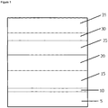
Figure 1 shows an example of the layer structure of an LED manufactured according to the present invention. -
Figures 2 shows a graph of the curvature of the wafer of the invention during the growth of the various layers required to form an LED. The x-axis shows the time in seconds. The Y-axis shows the curvature in km-1. -
Figure 3 shows two examples of the layers of the LED showing a SiNx interlayer, penetrating GaN and n-type GaN. It will be appreciated that these examples are not limiting on the scope of the invention. Further layers or replacement layers may be included in other examples. - The following key applies to the labels shown in
figure 3 :Letter Label A Mg-doped GaN layer B InGaN/GaN MQW C Si-doped GaN layer D Nid-doped GaN layer E AlGaN buffer layer F AlN nucleation layer G Si substrate H 3 dimensional GaN I SiNx interlayer (IL) - In this example GaN structures are grown on either 5.08 cm (2-inch) or 15.24cm (6-inch) Si (111) substrates 5 by metalorganic vapour phase epitaxy (MOVPE) in a 6x2" Aixtron CCS reactor using a 15.24cm x 5.04cm (6x2") or 2.54cm x 15.24cm (1×6") susceptor. 5.08 cm (2-inch) substrates are not in accordance with the invention. Trimethylgallium (TMG), trimethylaluminium (TMA) and trimethylindium (TMI) were used as group-III precursors, while ammonia was used as the nitrogen source. Silane (SiH4) and cyclopentadienyl magnesium (Cp2Mg) are used as the sources of n-type and p type dopants, respectively.
- A flat, crack-free and uniform GaN-based LED structure was grown on 15.24cm (6-inch) Si (111) substrate 5 by metal-organic vapour phase epitaxy (MOVPE). The as-supplied Si (111) substrates 5 were first annealed in the reactor to remove the native oxide layer. This was followed by the growth of an
AIN nucleation layer 10 which prevents Ga from reacting with the Si substrate. AnAIGaN buffer layer 15 was then grown to control the stress. TheAIN nucleation layer 10 and gradedAIGaN buffer layer 15 were employed for stress management, giving wafers with a radius of curvature >60 m for a total LED structure thickness of 2.5 µm. To reduce the dislocation density, an in-situ SiNx interlayer (not shown) was grown within theGaN layer 20 by partial deposition of theGaN layer 20, growing the interlayer and then completing theGaN layer 20. The temperature was decreased to 950 °C for the deposition of the SiNxinterlayer and regrowth started at 970 °C to form faceted islands, and then changed to 1050 °C for slow growth of the GaN layer to coalesce the film. After the film was fully coalesced, the growth conditions were set for a faster GaN growth. - After that, a Si-doped
GaN layer 25 with thickness of 1µm was grown. For LED structures, the growth temperature was then reduced and a N2 atmosphere used for the growth of the multiple quantum well (MQW)active region 30. The Mg-dopedGaN capping layer 35 was deposited in a H2 ambient. After the growth, in-situ annealing was carried out in a N2 atmosphere to activate the acceptors. - After growth the structures were characterised using a PANalytical MRD high resolution X-ray diffractometer and a Philips CM30 TEM operating at 300kV. A Digital Instruments Dimension 3100 atomic force microscope (AFM) was used to study the surface morphology. The wafer surface features were also examined using a graphic-EYE whole-wafer optical imaging system to show any surface cracks and roughness. The wafer curvature across the whole wafer and surface height were measured ex-situ using a KSA multi-beam optical sensor (MOS) ultrascantm instrument. PL and thickness maps were collected using an Accent RPM2000 PL mapping system.
- This example was repeated and the following structures were produced.

- The thickness of the AlxGa1-xN stress control layer in each example was chosen to ensure a flat crack-free final wafer. This thickness can depend to some extent on the thickness of the substrate, the thickness of the AIN nucleation layer and the thicknesses of the various GaN layers, both doped and undoped.
- In examples A-C the composition of the AlxGa1-xN layer varies linearly with distance from the nucleation layer, with x decreasing from 0.88 at the interface with AIN to 0.3 at the interface with the GaN layer. Similarly, in example D x decreases from 0.88 at the interface with AIN to 0.2 at the interface with the GaN layer. In example E the AlxGa1-xN is formed in discrete layers with different values of x. In examples A and D, a single SiNx interlayer was used between the GaN lower layer and the GaN upper layer. In examples B, C and E, a single SiNx interlayer was used between the GaN lower layer and the doped GaN layer. The silicon doping in the doped GaN layers had a constant value of 4x1018cm-3 on the top surface. The SiNx interlayer in each example had a thickness of about 2.5nm.
- The LED wafers could be characterised using X-ray diffraction (XRD), atomic force microscopy (AFM), transmission electron microscopy (TEM), photoluminescence (PL), ex-situ wafer curvature mapping and optical imaging techniques. Such techniques are well known in the art and a skilled man could select and employ the appropriate techniques to measure all of the layer thicknesses disclosed herein.
- A commercially available Epicurve®TT sensor (Laytec GmbH) was used to give emissivity-corrected real-time temperature and wafer curvature measurement and an Argus (Aixtron) in-situ temperature profiler was installed on top of the reactor to provide a complete temperature map of the wafer.
Figure 2 shows a trace of the curvature of the wafer during the manufacturing process for a wafer. - As can be seen in
figure 2 , the curvature of the wafers varies throughout the process. - Between 1000s and 3000s the substrate was annealed and plateaued at 25/km. Then a 200nm AIN nucleation layer was formed which increased the concave form of the wafer. At 7500s the AIGaN buffer layer was formed, and then a GaN layer containing a single interlayer to a total thickness of 1.3µm. At 12500 a Si-doped GaN layer was formed. Between 14000s and 18000s InGaN-GaN multi quantum wells (MQW) were formed before the wafer composite was allowed to cool. During cooling the curvature dropped from -150/km to +25/km.
- From the curvature data, it is clearly seen that the wafer bow changes during the growth as a function of the thicknesses of the various layers. It is evident that compressive stress has been introduced during the growth of the AIGaN buffer layer and Si-doped GaN layer, changing the wafer bow from concave to convex. Flat wafers are achieved at room temperature by this tensile stress compensation method.
- The preferred MOVPE reactor is a 6×2" CCS-MOCVD reactor with an Aixtron Argus installed. The Argus comprises a multi-element photodiode array in a novel configuration that utilizes an optical path through the reactor showerhead injection tubes. This allows a large number of discrete measurement points from which temperature data regarding wafer and susceptor surfaces can be acquired. Essentially, this allows the measurement of the surface temperature across the whole wafer during growth.
- From the in-situ curvature data, it is possible to see from the wafer bow where the wafer to substrate separation is increasing, and so where the temperature of the wafer will decrease. During growth the heater zone settings can then be adjusted to maintain a flat temperature profile. The PDA data is used to confirm that the resulting temperature profile across the wafer is flat. Temperature uniformity during growth is important to maintain the uniformity of the LED wavelength and intensity and to minimise slip in the Silicon.
- The growth of GaN on Si substrates usually starts with an AIN nucleation layer, to prevent Ga from reacting with Si and causing melt-back etching. A TMA pre-dose is a widely used method for the deposition of AIN to protect the Si substrate from nitridation, although it is found that the quality of the AIN nucleation layer is strongly affected by the growth temperature, the TMA pre-dose time and the thickness of the nucleation layer. The layer of AIN is desired to coalesce to great degree, showing a smooth surface with a root mean square (RMS) roughness ∼0.5 nm for a 25 µm2 area. A smooth (RMS roughness less than 1nm) AIN surface minimizes the crystal misorientation and reduces the cracking density in the subsequent GaN layer.
- Due to the larger in-plane lattice parameter of GaN compared to AIN, a GaN or AIGaN layer will be under compression when grown on AIN. This compressive stress in the (AI)GaN layer can be used to bend the Si wafer at the growth temperature to compensate for the wafer bow which will occur as a result of the tensile stress (arising from the large difference in thermal expansion coefficient between GaN and Si) during cooling to room temperature. The Al fraction in the AIGaN buffer layer can be either step-graded or continuously graded and both cases were found to be effective in terms of the introduction of compressive stress at growth temperatures.
- AIN deposition causes tensile stress, which increases with film thickness, possibly due to the layer coalescence. Similarly, thicker AIGaN buffer layers (at least up to 1.3 µm) introduce more compressive stress, enabling the growth of a thicker crack-free GaN layer. The optimised AIGaN buffer layer thickness depends on the thickness of the GaN layer required.
- Because of the large lattice mismatch between Si and AIGaN, GaN structures grown on Si substrates usually have a high initial dislocation density, which is undesirable for high performance devices. The difficulty of achieving low dislocation density for GaN on Si arises not only from the large lattice mismatch, but also due to the limited thickness of crack-free GaN that can be grown. To reduce the dislocation density, one or more SiNx interlayers (IL) can be incorporated into the GaN layer.
- Usually, a greater reduction in the threading dislocation (TD) density can be achieved by using thicker SiNx interlayers and longer coalescence times for the subsequent GaN layer on top of the interlayer. However, the challenge of using this TD reduction method for growth on Si is the limited thickness of crack-free GaN that can be deposited, while maintaining a low wafer bow.
- A graded AIGaN buffer layer was grown on an AIN/Si template, followed by 300 nm thick GaN layer at 1020°C. The temperature was then decreased to 950°C for the deposition of the SiNx interlayer and regrowth started at 970°C to form faceted islands and then changed to 1050°C for slow growth of the GaN layer to coalesce the film. After the film is fully coalesced growth conditions were set for faster GaN growth. The thickness of GaN required to fully coalesce the film after the deposition of SiNx depends on the deposition time of SiNx IL, as well as the growth conditions of the GaN regrowth on top. The TD density of approximately 6x108 cm-2 was obtained together with flat crack-free wafers. Preferred TD densities are less than 5x109 cm-2, more preferably less than 1x109 cm-2, more preferably less than 8x108 cm-2.
- After the growth of the AIGaN buffer layer, nominally undoped GaN of 100-400 nm thick is grown, followed by the deposition of the SiNx interlayer and further GaN growth. The two GaN regions (∼600 nm total) are kept nominally undoped to aid the coalescence of GaN film and also to prevent the introduction of additional TDs caused by Si-doping. The Si-doping profile of GaN was graded from low doping level to highly doped.
- Advantageously, the present invention allows the growth of crack-free n-type GaN (<2 microns) of low dislocation density on Si substrates. Equally, such layers could be grown on other substrates, especially those where the difference in lattice parameters dictate that thicker layers would be prone to wafer bending and cracking of the n-doped layer.
- Accordingly, the present invention enables a greater rate of threading dislocation reduction within the critical thickness to achieve device quality materials. As a consequence, the method reduces epitaxy growth time and epitaxy cost. In addition, since the further layers keep carriers away from defective regions (closer to the substrate and, in particular, around the GaN islands grown through the SiNx interlayer), a more reliable and higher efficiency LED device can be obtained.
Claims (14)
- A semiconductor wafer having a diameter of at least 15.24 cm (6 inches), comprising:a substrate layer consisting of silicon and unavoidable impurities;a first GaN layer having one or more SiNx interlayers therein;an AIGaN buffer layer consisting of two or more AIGaN layers between the substrate layer and the first GaN layer, wherein each layer has the formula AlxGa1-xN and the value of x in each layer is a value from 0.01 to less than 1 and the values of x in the two or more AIGaN layers differ by from 0.5 to 0.1, wherein the layers are arranged so that the values of x across the buffer layer and hence the concentration of aluminium decreases across the thickness of the buffer layer away from the silicon substrate; andan AIN layer between the substrate layer and the AIGaN layers;wherein in the first GaN layer at least one SiNx interlayer has GaN penetrated through one or more portions of said SiNx interlayer and has a thickness of from 2 to 8nm;wherein the thickness of the substrate layer is from 275 to 1000µm, the thickness of the AIN layer is from 10 to 300nm, the thickness of the first GaN layer is from 600 to 1200nm, including the thickness of the one or more SiNx interlayers, and the thickness of the AIGaN buffer layer is from 200 to 800nm.
- The semiconductor wafer of claim 1, wherein the first GaN layer is not intentionally doped, and/or has two or more SiNx interlayers therein.
- A semiconductor wafer according to any of the preceding claims, wherein GaN penetrates through one or more portions of at least one SiNx interlayer to form discrete crystalline structures within the GaN enclosing the SiNx interlayer.
- A semiconductor wafer according to any of the preceding claims, wherein the GaN penetrates through a plurality of portions of said SiNx interlayer across said interlayer.
- The semiconductor wafer according to any preceding claim, further comprising a second GaN layer on the first GaN layer, wherein the second GaN layer is intentionally doped,
preferably wherein the second GaN layer is n-doped, preferably with silicon or germanium. - The semiconductor wafer according to claim 5, wherein the second GaN layer is a compositionally graded Si- or Ge-doped GaN layer formed on the first GaN layer so that the amount of Si or Ge respectively increases across the thickness of the layer away from the GaN layer.
- The semiconductor wafer according to any of claims 5 or 6, further comprising a p-doped semiconductor layer formed on the second GaN layer.
- The semiconductor wafer of claim 7, further comprising a layer of multiple quantum wells, MQWs, formed between the second GaN layer and the p-doped semiconductor layer, and wherein the thickness of the layer of MQWs is preferably from 10 to 200nm.
- A product comprising the semiconductor wafer of any of the preceding claims, wherein the product is an LED or a Solar Cell.
- The semiconductor wafer of any of the preceding claims, wherein the wafer has a diameter of at least 8 inches.
- A semiconductor device comprising a semiconductor wafer as defined in any of claims 1 to 9.
- A process for forming a semiconductor wafer according to any of claims 1-8 and 10, wherein the layers are sequentially formed on the substrate using metalorganic vapour phase epitaxy, MOVPE, growth procedure.
- The process according to claim 12, wherein after the formation of one of said SiNx interlayers, GaN is deposited to penetrate through one or more portions of said SiNx interlayer, preferably wherein the GaN deposited to penetrate through one or more portions of said SiNx interlayer is deposited at a temperature of from 900 to 1050°C and a V/III ratio of less than 1000:1.
- The process according to claim 13, wherein at least two or more of the layers are deposited in a single MOVPE process carried out in a single MOVPE chamber.
Applications Claiming Priority (2)
| Application Number | Priority Date | Filing Date | Title |
|---|---|---|---|
| GB1019301.9A GB2485418B (en) | 2010-11-15 | 2010-11-15 | Semiconductor materials |
| PCT/GB2011/001474 WO2012066269A1 (en) | 2010-11-15 | 2011-10-12 | Semiconductor wafer comprising gallium nitride layer having one or more silicon nitride interlayer therein |
Publications (2)
| Publication Number | Publication Date |
|---|---|
| EP2641267A1 EP2641267A1 (en) | 2013-09-25 |
| EP2641267B1 true EP2641267B1 (en) | 2020-03-18 |
Family
ID=43431470
Family Applications (1)
| Application Number | Title | Priority Date | Filing Date |
|---|---|---|---|
| EP11773114.1A Active EP2641267B1 (en) | 2010-11-15 | 2011-10-12 | Semiconductor wafer comprising gallium nitride layer having one or more silicon nitride interlayer therein |
Country Status (5)
| Country | Link |
|---|---|
| US (1) | US9142723B2 (en) |
| EP (1) | EP2641267B1 (en) |
| CN (1) | CN103348447B (en) |
| GB (1) | GB2485418B (en) |
| WO (1) | WO2012066269A1 (en) |
Families Citing this family (41)
| Publication number | Priority date | Publication date | Assignee | Title |
|---|---|---|---|---|
| JP2013145867A (en) * | 2011-12-15 | 2013-07-25 | Hitachi Cable Ltd | Nitride semiconductor template, and light-emitting diode |
| US9896779B2 (en) | 2012-03-21 | 2018-02-20 | Freiberger Compound Materials Gmbh | Method for producing III-N single crystals, and III-N single crystal |
| KR20140022136A (en) * | 2012-08-13 | 2014-02-24 | 삼성전자주식회사 | Semiconductor light emitting device |
| DE102012217631B4 (en) * | 2012-09-27 | 2022-05-25 | OSRAM Opto Semiconductors Gesellschaft mit beschränkter Haftung | Optoelectronic component with a layer structure |
| GB201217617D0 (en) | 2012-10-02 | 2012-11-14 | Kappers Menno | Semiconductor materials |
| US20140158976A1 (en) | 2012-12-06 | 2014-06-12 | Sansaptak DASGUPTA | Iii-n semiconductor-on-silicon structures and techniques |
| SG10201705301QA (en) * | 2012-12-26 | 2017-07-28 | Agency Science Tech & Res | A semiconductor device for high-power applications |
| CN103123948A (en) * | 2013-01-15 | 2013-05-29 | 中国电子科技集团公司第五十五研究所 | Low-bending silicon-based III-nitride epitaxial wafer and growth method thereof |
| CN104167476A (en) * | 2013-05-20 | 2014-11-26 | 南通同方半导体有限公司 | Light-emitting diode structure capable of reducing blue-light LED defect density |
| JP6270536B2 (en) * | 2013-06-27 | 2018-01-31 | 株式会社東芝 | Nitride semiconductor device, nitride semiconductor wafer, and method of forming nitride semiconductor layer |
| JP6302254B2 (en) * | 2014-01-15 | 2018-03-28 | 株式会社東芝 | Nitride semiconductor device, nitride semiconductor wafer, and method of manufacturing nitride semiconductor device |
| US9520696B2 (en) | 2014-03-04 | 2016-12-13 | Princeton Optronics Inc. | Processes for making reliable VCSEL devices and VCSEL arrays |
| TWI550902B (en) * | 2014-04-02 | 2016-09-21 | 國立交通大學 | Light-emitting diode component |
| DE102014105303A1 (en) * | 2014-04-14 | 2015-10-15 | Osram Opto Semiconductors Gmbh | Method for producing a layer structure as a buffer layer of a semiconductor device and layer structure as a buffer layer of a semiconductor device |
| KR102188493B1 (en) | 2014-04-25 | 2020-12-09 | 삼성전자주식회사 | Method of growing nitride single crystal and method of manufacturing nitride semiconductor device |
| CN103985799B (en) * | 2014-06-05 | 2017-03-22 | 天津三安光电有限公司 | Light-emitting diode and manufacturing method thereof |
| CN105274496B (en) * | 2014-06-17 | 2019-01-15 | 北京大学 | Mutation formula impact air-flow grows the method for SiNx mask layer online in a kind of MOCVD |
| CN105810725A (en) * | 2014-12-31 | 2016-07-27 | 中晟光电设备(上海)股份有限公司 | Silicon-based gallium nitride semiconductor wafer and manufacturing method thereof |
| FR3031833B1 (en) * | 2015-01-21 | 2018-10-05 | Centre National De La Recherche Scientifique (Cnrs) | PROCESS FOR MANUFACTURING A PASSIVE ELEMENTS III-BASED NITRIDE SEMICONDUCTOR STRUCTURE AND SUCH A STRUCTURE |
| FR3031834B1 (en) * | 2015-01-21 | 2018-10-05 | Centre National De La Recherche Scientifique (Cnrs) | FABRICATION OF A SEMICONDUCTOR SUPPORT BASED ON ELEMENT III NITRIDE |
| JP6480244B2 (en) * | 2015-04-10 | 2019-03-06 | 株式会社ニューフレアテクノロジー | Vapor growth method |
| KR20250069970A (en) * | 2016-01-20 | 2025-05-20 | 메사추세츠 인스티튜트 오브 테크놀로지 | Fabrication of a device on a carrier substrate |
| CN106128948A (en) * | 2016-07-26 | 2016-11-16 | 中国科学院半导体研究所 | Strain modulating layer is utilized to reduce structure and the method for GaN layer threading dislocation on a si substrate |
| US9917156B1 (en) | 2016-09-02 | 2018-03-13 | IQE, plc | Nucleation layer for growth of III-nitride structures |
| US10205303B1 (en) | 2017-10-18 | 2019-02-12 | Lumentum Operations Llc | Vertical-cavity surface-emitting laser thin wafer bowing control |
| TWI631668B (en) * | 2017-11-22 | 2018-08-01 | Elite Advanced Laser Corporation | Nitride semiconductor structure |
| US10304881B1 (en) | 2017-12-15 | 2019-05-28 | Atomera Incorporated | CMOS image sensor with buried superlattice layer to reduce crosstalk |
| US10361243B2 (en) * | 2017-12-15 | 2019-07-23 | Atomera Incorporated | Method for making CMOS image sensor including superlattice to enhance infrared light absorption |
| US10355151B2 (en) | 2017-12-15 | 2019-07-16 | Atomera Incorporated | CMOS image sensor including photodiodes with overlying superlattices to reduce crosstalk |
| US10276625B1 (en) | 2017-12-15 | 2019-04-30 | Atomera Incorporated | CMOS image sensor including superlattice to enhance infrared light absorption |
| US10461118B2 (en) | 2017-12-15 | 2019-10-29 | Atomera Incorporated | Method for making CMOS image sensor including photodiodes with overlying superlattices to reduce crosstalk |
| US10396223B2 (en) | 2017-12-15 | 2019-08-27 | Atomera Incorporated | Method for making CMOS image sensor with buried superlattice layer to reduce crosstalk |
| DE102018101558A1 (en) * | 2018-01-24 | 2019-07-25 | Osram Opto Semiconductors Gmbh | A method of fabricating a nitride compound semiconductor device |
| CN108598234A (en) * | 2018-04-26 | 2018-09-28 | 吉林大学 | In a kind of reduction SiC substrate in GaN film tensile stress epitaxial structure and preparation method thereof |
| CN109686823B (en) * | 2018-11-26 | 2021-10-08 | 华灿光电(浙江)有限公司 | A kind of gallium nitride-based light-emitting diode epitaxial wafer and manufacturing method thereof |
| CN112018199B (en) * | 2019-05-30 | 2023-04-07 | 南京信息工程大学 | High-quality nonpolar AlGaN micro-nano composite structure and processing method thereof |
| TWI698914B (en) * | 2019-07-19 | 2020-07-11 | 環球晶圓股份有限公司 | Semiconductor epitaxial structure and method of forming the same |
| CN111063726A (en) * | 2019-12-20 | 2020-04-24 | 西安电子科技大学芜湖研究院 | Epitaxial structure of a Si-based gallium nitride device |
| WO2022068256A1 (en) * | 2020-09-30 | 2022-04-07 | 苏州能讯高能半导体有限公司 | Epitaxial structure of semiconductor device and preparation method therefor |
| CN112103178A (en) * | 2020-10-30 | 2020-12-18 | 深圳第三代半导体研究院 | GaN film coated on copper surface and preparation method thereof |
| CN117954471A (en) * | 2022-10-21 | 2024-04-30 | 苏州能讯高能半导体有限公司 | Epitaxial structure of semiconductor device, preparation method of epitaxial structure and semiconductor device |
Citations (2)
| Publication number | Priority date | Publication date | Assignee | Title |
|---|---|---|---|---|
| US20020074552A1 (en) * | 2000-12-14 | 2002-06-20 | Weeks T. Warren | Gallium nitride materials and methods |
| US20070267654A1 (en) * | 2006-05-09 | 2007-11-22 | Arpan Chakraborty | In-situ defect reduction techniques for nonpolar and semipolar (Al,Ga, In)N |
Family Cites Families (13)
| Publication number | Priority date | Publication date | Assignee | Title |
|---|---|---|---|---|
| EP1007768A4 (en) * | 1997-07-03 | 2003-07-16 | Cbl Technologies | ELIMINATION OF THERMAL INADEQUATION DEFECTS OF EPITAXIC FILMS BY SEPARATING THE FILM SUBSTRATE AT GROWTH TEMPERATURE |
| US6252261B1 (en) * | 1998-09-30 | 2001-06-26 | Nec Corporation | GaN crystal film, a group III element nitride semiconductor wafer and a manufacturing process therefor |
| US6610144B2 (en) * | 2000-07-21 | 2003-08-26 | The Regents Of The University Of California | Method to reduce the dislocation density in group III-nitride films |
| KR20040008522A (en) * | 2002-07-18 | 2004-01-31 | 엘지전자 주식회사 | Method for elevating GaN crystallization |
| US20070184671A1 (en) * | 2003-05-30 | 2007-08-09 | Showa Denko K.K. | Method for production of group lll nitride semiconductor device |
| WO2005036658A1 (en) * | 2003-10-14 | 2005-04-21 | Showa Denko K.K. | Group-iii nitride semiconductor device |
| US7687827B2 (en) | 2004-07-07 | 2010-03-30 | Nitronex Corporation | III-nitride materials including low dislocation densities and methods associated with the same |
| KR100609583B1 (en) * | 2004-08-26 | 2006-08-09 | 엘지이노텍 주식회사 | Nitride semiconductor light emitting device and manufacturing method |
| US20060073681A1 (en) * | 2004-09-08 | 2006-04-06 | Han Sang M | Nanoheteroepitaxy of Ge on Si as a foundation for group III-V and II-VI integration |
| WO2007102627A1 (en) * | 2005-07-06 | 2007-09-13 | Lg Innotek Co., Ltd | Nitride semiconductor led and fabrication metho thereof |
| KR200408522Y1 (en) * | 2005-11-28 | 2006-02-13 | 윤영민 | Rubber * plastic bag exit stopper |
| KR100756841B1 (en) | 2006-03-13 | 2007-09-07 | 서울옵토디바이스주식회사 | Light Emitting Diode Having Al-An-Bn Buffer Layer And Method Of Manufacturing The Same |
| US8803189B2 (en) * | 2008-08-11 | 2014-08-12 | Taiwan Semiconductor Manufacturing Company, Ltd. | III-V compound semiconductor epitaxy using lateral overgrowth |
-
2010
- 2010-11-15 GB GB1019301.9A patent/GB2485418B/en active Active
-
2011
- 2011-10-12 CN CN201180065064.4A patent/CN103348447B/en active Active
- 2011-10-12 US US13/885,346 patent/US9142723B2/en active Active
- 2011-10-12 WO PCT/GB2011/001474 patent/WO2012066269A1/en not_active Ceased
- 2011-10-12 EP EP11773114.1A patent/EP2641267B1/en active Active
Patent Citations (2)
| Publication number | Priority date | Publication date | Assignee | Title |
|---|---|---|---|---|
| US20020074552A1 (en) * | 2000-12-14 | 2002-06-20 | Weeks T. Warren | Gallium nitride materials and methods |
| US20070267654A1 (en) * | 2006-05-09 | 2007-11-22 | Arpan Chakraborty | In-situ defect reduction techniques for nonpolar and semipolar (Al,Ga, In)N |
Non-Patent Citations (2)
| Title |
|---|
| MOON Y T ET AL: "A study of the morphology of GaN seed layers on in situ deposited Si"xN"y and its effect on properties of overgrown GaN epilayers", JOURNAL OF CRYSTAL GROWTH, ELSEVIER, AMSTERDAM, NL, vol. 291, no. 1, 15 May 2006 (2006-05-15), pages 301 - 308, XP028016613, ISSN: 0022-0248, [retrieved on 20060515], DOI: 10.1016/J.JCRYSGRO.2006.03.010 * |
| R. F. ZHANG ET AL: "Understanding why the thinnest SiNx interface in transition-metal nitrides is stronger than the ideal bulk crystal", PHYSICAL REVIEW. B, vol. 81, no. 24, 1 June 2010 (2010-06-01), US, XP055594863, ISSN: 1098-0121, DOI: 10.1103/PhysRevB.81.245418 * |
Also Published As
| Publication number | Publication date |
|---|---|
| EP2641267A1 (en) | 2013-09-25 |
| US20130270575A1 (en) | 2013-10-17 |
| GB201019301D0 (en) | 2010-12-29 |
| WO2012066269A1 (en) | 2012-05-24 |
| GB2485418B (en) | 2014-10-01 |
| CN103348447B (en) | 2016-08-17 |
| CN103348447A (en) | 2013-10-09 |
| GB2485418A (en) | 2012-05-16 |
| US9142723B2 (en) | 2015-09-22 |
Similar Documents
| Publication | Publication Date | Title |
|---|---|---|
| US9142723B2 (en) | Semiconductor wafer comprising gallium nitride layer having one or more silicon nitride interlayer therein | |
| CN101427391B (en) | Nitride semiconductor component and manufacturing process thereof | |
| US8643024B2 (en) | In-situ defect reduction techniques for nonpolar and semipolar (Al, Ga, In)N | |
| EP2313543B1 (en) | Growth of planar and semi-polar {1 1-2 2} gallium nitride with hydride vapor phase epitaxy (hvpe) | |
| KR102016046B1 (en) | Method for manufacturing a thick epitaxial layer of gallium nitride on a silicon or similar substrate and layer obtained using said method | |
| EP2064730B1 (en) | Nitride semiconductor structures with interlayer structures and methods of fabricating nitride semiconductor structures with interlayer structures | |
| EP1211715B1 (en) | A method for fabricating a III-V nitride film | |
| CN102064091B (en) | Nitride semiconductor component and manufacturing process thereof | |
| KR101384042B1 (en) | Method of manufacturing nitride semiconductor layer | |
| US9276070B2 (en) | Semiconductor structures including stacks of indium gallium nitride layers | |
| US20130168833A1 (en) | METHOD FOR ENHANCING GROWTH OF SEMIPOLAR (Al,In,Ga,B)N VIA METALORGANIC CHEMICAL VAPOR DEPOSITION | |
| TWI521733B (en) | Method for producing a gallium-containing group III nitride semiconductor | |
| EP2904630B1 (en) | Semiconductor material | |
| WO2006012298A9 (en) | Gallium nitride material and methods associated with the same | |
| EP2495358A1 (en) | Methods of forming III/V semiconductor materials, and semiconductor structures formed using such methods | |
| CN108110093A (en) | Silicon substrate GaN-based LED epitaxial growth methods | |
| EP3050075A1 (en) | A semiconductor wafer and a method for producing the semiconductor wafer | |
| JP7811397B2 (en) | GaN-on-Si epiwafer with strain-decoupled substack | |
| Gangopadhyay et al. | Growth and formation of InGaN and GaN nano-structures studied by STM | |
| JP2009208989A (en) | Compound semiconductor substrate and method for producing the same | |
| Gangopadhyay et al. | Surface Morphology and Island Shape of MOVPE Grown InGaN Nano-Island Ensembles Studied by STM |
Legal Events
| Date | Code | Title | Description |
|---|---|---|---|
| PUAI | Public reference made under article 153(3) epc to a published international application that has entered the european phase |
Free format text: ORIGINAL CODE: 0009012 |
|
| 17P | Request for examination filed |
Effective date: 20130604 |
|
| AK | Designated contracting states |
Kind code of ref document: A1 Designated state(s): AL AT BE BG CH CY CZ DE DK EE ES FI FR GB GR HR HU IE IS IT LI LT LU LV MC MK MT NL NO PL PT RO RS SE SI SK SM TR |
|
| DAX | Request for extension of the european patent (deleted) | ||
| RAP1 | Party data changed (applicant data changed or rights of an application transferred) |
Owner name: INTELLEC LIMITED |
|
| RIN1 | Information on inventor provided before grant (corrected) |
Inventor name: INTELLEC LIMITED |
|
| DIN1 | Information on inventor provided before grant (deleted) | ||
| RIN1 | Information on inventor provided before grant (corrected) |
Inventor name: ZHU, DANDAN Inventor name: HUMPHREYS, COLIN Inventor name: KAPPERS, MENNO Inventor name: MCALEESE, CLIFFORD Inventor name: LIU, ZHENYU |
|
| 111Z | Information provided on other rights and legal means of execution |
Free format text: AL AT BE BG CH CY CZ DE DK EE ES FI FR GB GR HR HU IE IS IT LT LU LV MC MK MT NL NO PL PT RO RS SE SI SK SM TR Effective date: 20151109 |
|
| STAA | Information on the status of an ep patent application or granted ep patent |
Free format text: STATUS: EXAMINATION IS IN PROGRESS |
|
| 17Q | First examination report despatched |
Effective date: 20180528 |
|
| RIC1 | Information provided on ipc code assigned before grant |
Ipc: H01L 31/0352 20060101ALI20190507BHEP Ipc: H01L 21/205 20060101AFI20190507BHEP Ipc: H01L 33/00 20100101ALN20190507BHEP Ipc: H01L 33/32 20100101ALI20190507BHEP Ipc: B82Y 20/00 20110101ALI20190507BHEP Ipc: H01L 31/075 20120101ALI20190507BHEP Ipc: H01L 21/02 20060101ALI20190507BHEP Ipc: H01L 31/18 20060101ALI20190507BHEP Ipc: H01L 33/12 20100101ALN20190507BHEP |
|
| RIC1 | Information provided on ipc code assigned before grant |
Ipc: H01L 21/02 20060101ALI20190917BHEP Ipc: H01L 33/32 20100101ALI20190917BHEP Ipc: H01L 21/205 20060101AFI20190917BHEP Ipc: H01L 33/00 20100101ALN20190917BHEP Ipc: H01L 31/0352 20060101ALI20190917BHEP Ipc: H01L 33/12 20100101ALN20190917BHEP Ipc: H01L 31/18 20060101ALI20190917BHEP Ipc: B82Y 20/00 20110101ALI20190917BHEP Ipc: H01L 31/075 20120101ALI20190917BHEP |
|
| GRAP | Despatch of communication of intention to grant a patent |
Free format text: ORIGINAL CODE: EPIDOSNIGR1 |
|
| STAA | Information on the status of an ep patent application or granted ep patent |
Free format text: STATUS: GRANT OF PATENT IS INTENDED |
|
| RIC1 | Information provided on ipc code assigned before grant |
Ipc: H01L 33/12 20100101ALN20190926BHEP Ipc: H01L 31/18 20060101ALI20190926BHEP Ipc: B82Y 20/00 20110101ALN20190926BHEP Ipc: H01L 31/0352 20060101ALI20190926BHEP Ipc: H01L 21/205 20060101AFI20190926BHEP Ipc: H01L 33/00 20100101ALN20190926BHEP Ipc: H01L 21/02 20060101ALI20190926BHEP Ipc: H01L 33/32 20100101ALI20190926BHEP Ipc: H01L 31/075 20120101ALI20190926BHEP |
|
| RIC1 | Information provided on ipc code assigned before grant |
Ipc: H01L 31/075 20120101ALI20191010BHEP Ipc: B82Y 20/00 20110101ALN20191010BHEP Ipc: H01L 33/32 20100101ALI20191010BHEP Ipc: H01L 21/205 20060101AFI20191010BHEP Ipc: H01L 33/00 20100101ALN20191010BHEP Ipc: H01L 21/02 20060101ALI20191010BHEP Ipc: H01L 31/18 20060101ALI20191010BHEP Ipc: H01L 33/12 20100101ALN20191010BHEP Ipc: H01L 31/0352 20060101ALI20191010BHEP |
|
| INTG | Intention to grant announced |
Effective date: 20191025 |
|
| GRAS | Grant fee paid |
Free format text: ORIGINAL CODE: EPIDOSNIGR3 |
|
| GRAA | (expected) grant |
Free format text: ORIGINAL CODE: 0009210 |
|
| STAA | Information on the status of an ep patent application or granted ep patent |
Free format text: STATUS: THE PATENT HAS BEEN GRANTED |
|
| AK | Designated contracting states |
Kind code of ref document: B1 Designated state(s): AL AT BE BG CH CY CZ DE DK EE ES FI FR GB GR HR HU IE IS IT LI LT LU LV MC MK MT NL NO PL PT RO RS SE SI SK SM TR |
|
| REG | Reference to a national code |
Ref country code: GB Ref legal event code: FG4D |
|
| REG | Reference to a national code |
Ref country code: DE Ref legal event code: R096 Ref document number: 602011065693 Country of ref document: DE |
|
| REG | Reference to a national code |
Ref country code: AT Ref legal event code: REF Ref document number: 1246892 Country of ref document: AT Kind code of ref document: T Effective date: 20200415 Ref country code: IE Ref legal event code: FG4D |
|
| PG25 | Lapsed in a contracting state [announced via postgrant information from national office to epo] |
Ref country code: NO Free format text: LAPSE BECAUSE OF FAILURE TO SUBMIT A TRANSLATION OF THE DESCRIPTION OR TO PAY THE FEE WITHIN THE PRESCRIBED TIME-LIMIT Effective date: 20200618 Ref country code: RS Free format text: LAPSE BECAUSE OF FAILURE TO SUBMIT A TRANSLATION OF THE DESCRIPTION OR TO PAY THE FEE WITHIN THE PRESCRIBED TIME-LIMIT Effective date: 20200318 Ref country code: FI Free format text: LAPSE BECAUSE OF FAILURE TO SUBMIT A TRANSLATION OF THE DESCRIPTION OR TO PAY THE FEE WITHIN THE PRESCRIBED TIME-LIMIT Effective date: 20200318 |
|
| REG | Reference to a national code |
Ref country code: NL Ref legal event code: MP Effective date: 20200318 |
|
| PG25 | Lapsed in a contracting state [announced via postgrant information from national office to epo] |
Ref country code: HR Free format text: LAPSE BECAUSE OF FAILURE TO SUBMIT A TRANSLATION OF THE DESCRIPTION OR TO PAY THE FEE WITHIN THE PRESCRIBED TIME-LIMIT Effective date: 20200318 Ref country code: GR Free format text: LAPSE BECAUSE OF FAILURE TO SUBMIT A TRANSLATION OF THE DESCRIPTION OR TO PAY THE FEE WITHIN THE PRESCRIBED TIME-LIMIT Effective date: 20200619 Ref country code: LV Free format text: LAPSE BECAUSE OF FAILURE TO SUBMIT A TRANSLATION OF THE DESCRIPTION OR TO PAY THE FEE WITHIN THE PRESCRIBED TIME-LIMIT Effective date: 20200318 Ref country code: SE Free format text: LAPSE BECAUSE OF FAILURE TO SUBMIT A TRANSLATION OF THE DESCRIPTION OR TO PAY THE FEE WITHIN THE PRESCRIBED TIME-LIMIT Effective date: 20200318 Ref country code: BG Free format text: LAPSE BECAUSE OF FAILURE TO SUBMIT A TRANSLATION OF THE DESCRIPTION OR TO PAY THE FEE WITHIN THE PRESCRIBED TIME-LIMIT Effective date: 20200618 |
|
| REG | Reference to a national code |
Ref country code: LT Ref legal event code: MG4D |
|
| PG25 | Lapsed in a contracting state [announced via postgrant information from national office to epo] |
Ref country code: NL Free format text: LAPSE BECAUSE OF FAILURE TO SUBMIT A TRANSLATION OF THE DESCRIPTION OR TO PAY THE FEE WITHIN THE PRESCRIBED TIME-LIMIT Effective date: 20200318 |
|
| PG25 | Lapsed in a contracting state [announced via postgrant information from national office to epo] |
Ref country code: SM Free format text: LAPSE BECAUSE OF FAILURE TO SUBMIT A TRANSLATION OF THE DESCRIPTION OR TO PAY THE FEE WITHIN THE PRESCRIBED TIME-LIMIT Effective date: 20200318 Ref country code: EE Free format text: LAPSE BECAUSE OF FAILURE TO SUBMIT A TRANSLATION OF THE DESCRIPTION OR TO PAY THE FEE WITHIN THE PRESCRIBED TIME-LIMIT Effective date: 20200318 Ref country code: LT Free format text: LAPSE BECAUSE OF FAILURE TO SUBMIT A TRANSLATION OF THE DESCRIPTION OR TO PAY THE FEE WITHIN THE PRESCRIBED TIME-LIMIT Effective date: 20200318 Ref country code: RO Free format text: LAPSE BECAUSE OF FAILURE TO SUBMIT A TRANSLATION OF THE DESCRIPTION OR TO PAY THE FEE WITHIN THE PRESCRIBED TIME-LIMIT Effective date: 20200318 Ref country code: PT Free format text: LAPSE BECAUSE OF FAILURE TO SUBMIT A TRANSLATION OF THE DESCRIPTION OR TO PAY THE FEE WITHIN THE PRESCRIBED TIME-LIMIT Effective date: 20200812 Ref country code: CZ Free format text: LAPSE BECAUSE OF FAILURE TO SUBMIT A TRANSLATION OF THE DESCRIPTION OR TO PAY THE FEE WITHIN THE PRESCRIBED TIME-LIMIT Effective date: 20200318 Ref country code: SK Free format text: LAPSE BECAUSE OF FAILURE TO SUBMIT A TRANSLATION OF THE DESCRIPTION OR TO PAY THE FEE WITHIN THE PRESCRIBED TIME-LIMIT Effective date: 20200318 Ref country code: IS Free format text: LAPSE BECAUSE OF FAILURE TO SUBMIT A TRANSLATION OF THE DESCRIPTION OR TO PAY THE FEE WITHIN THE PRESCRIBED TIME-LIMIT Effective date: 20200718 |
|
| REG | Reference to a national code |
Ref country code: AT Ref legal event code: MK05 Ref document number: 1246892 Country of ref document: AT Kind code of ref document: T Effective date: 20200318 |
|
| REG | Reference to a national code |
Ref country code: DE Ref legal event code: R097 Ref document number: 602011065693 Country of ref document: DE |
|
| PLBE | No opposition filed within time limit |
Free format text: ORIGINAL CODE: 0009261 |
|
| STAA | Information on the status of an ep patent application or granted ep patent |
Free format text: STATUS: NO OPPOSITION FILED WITHIN TIME LIMIT |
|
| PG25 | Lapsed in a contracting state [announced via postgrant information from national office to epo] |
Ref country code: ES Free format text: LAPSE BECAUSE OF FAILURE TO SUBMIT A TRANSLATION OF THE DESCRIPTION OR TO PAY THE FEE WITHIN THE PRESCRIBED TIME-LIMIT Effective date: 20200318 Ref country code: AT Free format text: LAPSE BECAUSE OF FAILURE TO SUBMIT A TRANSLATION OF THE DESCRIPTION OR TO PAY THE FEE WITHIN THE PRESCRIBED TIME-LIMIT Effective date: 20200318 Ref country code: DK Free format text: LAPSE BECAUSE OF FAILURE TO SUBMIT A TRANSLATION OF THE DESCRIPTION OR TO PAY THE FEE WITHIN THE PRESCRIBED TIME-LIMIT Effective date: 20200318 |
|
| 26N | No opposition filed |
Effective date: 20201221 |
|
| PG25 | Lapsed in a contracting state [announced via postgrant information from national office to epo] |
Ref country code: PL Free format text: LAPSE BECAUSE OF FAILURE TO SUBMIT A TRANSLATION OF THE DESCRIPTION OR TO PAY THE FEE WITHIN THE PRESCRIBED TIME-LIMIT Effective date: 20200318 |
|
| PG25 | Lapsed in a contracting state [announced via postgrant information from national office to epo] |
Ref country code: SI Free format text: LAPSE BECAUSE OF FAILURE TO SUBMIT A TRANSLATION OF THE DESCRIPTION OR TO PAY THE FEE WITHIN THE PRESCRIBED TIME-LIMIT Effective date: 20200318 |
|
| REG | Reference to a national code |
Ref country code: CH Ref legal event code: PL |
|
| PG25 | Lapsed in a contracting state [announced via postgrant information from national office to epo] |
Ref country code: LU Free format text: LAPSE BECAUSE OF NON-PAYMENT OF DUE FEES Effective date: 20201012 Ref country code: MC Free format text: LAPSE BECAUSE OF FAILURE TO SUBMIT A TRANSLATION OF THE DESCRIPTION OR TO PAY THE FEE WITHIN THE PRESCRIBED TIME-LIMIT Effective date: 20200318 |
|
| REG | Reference to a national code |
Ref country code: BE Ref legal event code: MM Effective date: 20201031 |
|
| PG25 | Lapsed in a contracting state [announced via postgrant information from national office to epo] |
Ref country code: CH Free format text: LAPSE BECAUSE OF NON-PAYMENT OF DUE FEES Effective date: 20201031 Ref country code: BE Free format text: LAPSE BECAUSE OF NON-PAYMENT OF DUE FEES Effective date: 20201031 Ref country code: LI Free format text: LAPSE BECAUSE OF NON-PAYMENT OF DUE FEES Effective date: 20201031 |
|
| PG25 | Lapsed in a contracting state [announced via postgrant information from national office to epo] |
Ref country code: TR Free format text: LAPSE BECAUSE OF FAILURE TO SUBMIT A TRANSLATION OF THE DESCRIPTION OR TO PAY THE FEE WITHIN THE PRESCRIBED TIME-LIMIT Effective date: 20200318 Ref country code: MT Free format text: LAPSE BECAUSE OF FAILURE TO SUBMIT A TRANSLATION OF THE DESCRIPTION OR TO PAY THE FEE WITHIN THE PRESCRIBED TIME-LIMIT Effective date: 20200318 Ref country code: CY Free format text: LAPSE BECAUSE OF FAILURE TO SUBMIT A TRANSLATION OF THE DESCRIPTION OR TO PAY THE FEE WITHIN THE PRESCRIBED TIME-LIMIT Effective date: 20200318 |
|
| PG25 | Lapsed in a contracting state [announced via postgrant information from national office to epo] |
Ref country code: MK Free format text: LAPSE BECAUSE OF FAILURE TO SUBMIT A TRANSLATION OF THE DESCRIPTION OR TO PAY THE FEE WITHIN THE PRESCRIBED TIME-LIMIT Effective date: 20200318 Ref country code: AL Free format text: LAPSE BECAUSE OF FAILURE TO SUBMIT A TRANSLATION OF THE DESCRIPTION OR TO PAY THE FEE WITHIN THE PRESCRIBED TIME-LIMIT Effective date: 20200318 |
|
| REG | Reference to a national code |
Ref country code: DE Ref legal event code: R079 Ref document number: 602011065693 Country of ref document: DE Free format text: PREVIOUS MAIN CLASS: H01L0021205000 Ipc: H10P0014240000 |
|
| PGFP | Annual fee paid to national office [announced via postgrant information from national office to epo] |
Ref country code: DE Payment date: 20251020 Year of fee payment: 15 |
|
| PGFP | Annual fee paid to national office [announced via postgrant information from national office to epo] |
Ref country code: GB Payment date: 20251020 Year of fee payment: 15 |
|
| PGFP | Annual fee paid to national office [announced via postgrant information from national office to epo] |
Ref country code: IT Payment date: 20251020 Year of fee payment: 15 |
|
| PGFP | Annual fee paid to national office [announced via postgrant information from national office to epo] |
Ref country code: FR Payment date: 20251017 Year of fee payment: 15 |
|
| PGFP | Annual fee paid to national office [announced via postgrant information from national office to epo] |
Ref country code: IE Payment date: 20251017 Year of fee payment: 15 |
|
| REG | Reference to a national code |
Ref country code: GB Ref legal event code: 732E Free format text: REGISTERED BETWEEN 20260219 AND 20260225 |