EP2639819A1 - Method for forming thermal oxide film of monocrystalline silicon wafer - Google Patents
Method for forming thermal oxide film of monocrystalline silicon wafer Download PDFInfo
- Publication number
- EP2639819A1 EP2639819A1 EP11839425.3A EP11839425A EP2639819A1 EP 2639819 A1 EP2639819 A1 EP 2639819A1 EP 11839425 A EP11839425 A EP 11839425A EP 2639819 A1 EP2639819 A1 EP 2639819A1
- Authority
- EP
- European Patent Office
- Prior art keywords
- temperature
- oxide film
- thermal oxide
- heat treatment
- treatment furnace
- Prior art date
- Legal status (The legal status is an assumption and is not a legal conclusion. Google has not performed a legal analysis and makes no representation as to the accuracy of the status listed.)
- Granted
Links
Images
Classifications
-
- H—ELECTRICITY
- H10—SEMICONDUCTOR DEVICES; ELECTRIC SOLID-STATE DEVICES NOT OTHERWISE PROVIDED FOR
- H10P—GENERIC PROCESSES OR APPARATUS FOR THE MANUFACTURE OR TREATMENT OF DEVICES COVERED BY CLASS H10
- H10P14/00—Formation of materials, e.g. in the shape of layers or pillars
- H10P14/60—Formation of materials, e.g. in the shape of layers or pillars of insulating materials
- H10P14/63—Formation of materials, e.g. in the shape of layers or pillars of insulating materials characterised by the formation processes
- H10P14/6302—Non-deposition formation processes
- H10P14/6322—Formation by thermal treatments
-
- H—ELECTRICITY
- H10—SEMICONDUCTOR DEVICES; ELECTRIC SOLID-STATE DEVICES NOT OTHERWISE PROVIDED FOR
- H10P—GENERIC PROCESSES OR APPARATUS FOR THE MANUFACTURE OR TREATMENT OF DEVICES COVERED BY CLASS H10
- H10P14/00—Formation of materials, e.g. in the shape of layers or pillars
- H10P14/20—Formation of materials, e.g. in the shape of layers or pillars of semiconductor materials
- H10P14/29—Formation of materials, e.g. in the shape of layers or pillars of semiconductor materials characterised by the substrates
- H10P14/2901—Materials
- H10P14/2913—Materials being Group IIB-VIA materials
- H10P14/2914—Oxides
-
- H—ELECTRICITY
- H10—SEMICONDUCTOR DEVICES; ELECTRIC SOLID-STATE DEVICES NOT OTHERWISE PROVIDED FOR
- H10P—GENERIC PROCESSES OR APPARATUS FOR THE MANUFACTURE OR TREATMENT OF DEVICES COVERED BY CLASS H10
- H10P14/00—Formation of materials, e.g. in the shape of layers or pillars
- H10P14/20—Formation of materials, e.g. in the shape of layers or pillars of semiconductor materials
- H10P14/34—Deposited materials, e.g. layers
- H10P14/3451—Structure
- H10P14/3452—Microstructure
- H10P14/3458—Monocrystalline
-
- H—ELECTRICITY
- H10—SEMICONDUCTOR DEVICES; ELECTRIC SOLID-STATE DEVICES NOT OTHERWISE PROVIDED FOR
- H10P—GENERIC PROCESSES OR APPARATUS FOR THE MANUFACTURE OR TREATMENT OF DEVICES COVERED BY CLASS H10
- H10P14/00—Formation of materials, e.g. in the shape of layers or pillars
- H10P14/60—Formation of materials, e.g. in the shape of layers or pillars of insulating materials
- H10P14/69—Inorganic materials
- H10P14/6903—Inorganic materials containing silicon
-
- H—ELECTRICITY
- H10—SEMICONDUCTOR DEVICES; ELECTRIC SOLID-STATE DEVICES NOT OTHERWISE PROVIDED FOR
- H10P—GENERIC PROCESSES OR APPARATUS FOR THE MANUFACTURE OR TREATMENT OF DEVICES COVERED BY CLASS H10
- H10P14/00—Formation of materials, e.g. in the shape of layers or pillars
- H10P14/60—Formation of materials, e.g. in the shape of layers or pillars of insulating materials
- H10P14/63—Formation of materials, e.g. in the shape of layers or pillars of insulating materials characterised by the formation processes
- H10P14/6302—Non-deposition formation processes
- H10P14/6304—Formation by oxidation, e.g. oxidation of the substrate
- H10P14/6306—Formation by oxidation, e.g. oxidation of the substrate of the semiconductor materials
- H10P14/6308—Formation by oxidation, e.g. oxidation of the substrate of the semiconductor materials of Group IV semiconductors
- H10P14/6309—Formation by oxidation, e.g. oxidation of the substrate of the semiconductor materials of Group IV semiconductors of silicon in uncombined form, i.e. pure silicon
-
- H—ELECTRICITY
- H10—SEMICONDUCTOR DEVICES; ELECTRIC SOLID-STATE DEVICES NOT OTHERWISE PROVIDED FOR
- H10P—GENERIC PROCESSES OR APPARATUS FOR THE MANUFACTURE OR TREATMENT OF DEVICES COVERED BY CLASS H10
- H10P14/00—Formation of materials, e.g. in the shape of layers or pillars
- H10P14/60—Formation of materials, e.g. in the shape of layers or pillars of insulating materials
- H10P14/63—Formation of materials, e.g. in the shape of layers or pillars of insulating materials characterised by the formation processes
- H10P14/6326—Deposition processes
- H10P14/6328—Deposition from the gas or vapour phase
- H10P14/6334—Deposition from the gas or vapour phase using decomposition or reaction of gaseous or vapour phase compounds, i.e. chemical vapour deposition
-
- H—ELECTRICITY
- H10—SEMICONDUCTOR DEVICES; ELECTRIC SOLID-STATE DEVICES NOT OTHERWISE PROVIDED FOR
- H10P—GENERIC PROCESSES OR APPARATUS FOR THE MANUFACTURE OR TREATMENT OF DEVICES COVERED BY CLASS H10
- H10P14/00—Formation of materials, e.g. in the shape of layers or pillars
- H10P14/60—Formation of materials, e.g. in the shape of layers or pillars of insulating materials
- H10P14/69—Inorganic materials
- H10P14/692—Inorganic materials composed of oxides, glassy oxides or oxide-based glasses
- H10P14/6921—Inorganic materials composed of oxides, glassy oxides or oxide-based glasses containing silicon
- H10P14/69215—Inorganic materials composed of oxides, glassy oxides or oxide-based glasses containing silicon the material being a silicon oxide, e.g. SiO2
Definitions
- the present invention relates to a thermal oxide film formation method for suppressing slip dislocation, etc. taking place when thermal oxide film is formed on a silicon single crystal wafer.
- a thermal oxide film on the surface of a silicon single crystal wafer e.g., silicon single crystal wafer is mounted on a heat treatment jig (frequently referred to as wafer boat) made of heat resistant material (e.g., quartz or SiC) to set such a jig within a tube for heat treatment furnace to perform heat treatment under oxidizing atmosphere.
- a heat treatment jig (frequently referred to as wafer boat) made of heat resistant material (e.g., quartz or SiC) to set such a jig within a tube for heat treatment furnace to perform heat treatment under oxidizing atmosphere.
- Control of film thickness of the thermal oxide film formed in this way is performed after subjected to calculation by the kind of the heat treatment atmosphere, the heat treatment temperature and/or heat treatment time.
- thermal oxide film to be formed on the surface of the silicon single crystal wafer although depending upon the purpose, in the case of fabricating a bonded SOI wafer including a thick buried oxide film layer (BOX layer) as described in the Patent Literature 1, a thick thermal oxide film is formed on at least one of two silicon single crystal wafers to be bonded and a bonding process is performed.
- BOX layer buried oxide film layer
- high temperature/long time heat treatment is performed under the atmosphere including water vapor such as wet O 2 oxidation or pyrogenic oxidation, etc. as the heat treatment atmosphere where oxidation rate is high.
- the present invention has been made in view of the above-described problems, and aims at providing a method of forming a thermal oxide film of preventing sticking onto a wafer boat taking place particularly in forming s thick oxide film to have ability to suppress occurrence of slip dislocation and/or crack of a silicon single crystal wafer during formation of the thermal oxide film.
- the present invention provides a method of forming a thermal oxide film on a silicon single crystal wafer, at least comprising: throwing the silicon single crystal wafer into a heat treatment furnace; elevating temperature of the heat treatment furnace up to a temperature T1 where a thermal oxide film is formed to form a thermal oxide film having a thickness d1; subsequently lowering the temperature of the heat treatment furnace down to a temperature lower than the temperature T1; and thereafter elevating the temperature of the heat treatment furnace up to a temperature T2 higher than the temperature T1 to additionally form a thermal oxide film having a thickness d2 thicker than the thickness d1.
- the thermal oxide film formed in this way warp phenomenon of wafer takes place resulting from a temperature difference between a wafer outer peripheral part and a central part occurring at the time of lowering temperature, and therefore a position in contact with a wafer boat for holding the wafer changes. For this reason, it is possible to prevent that the wafer is stuck onto the wafer boat by the thermal oxide film.
- the thermal oxide film formed during oxidation at the temperature T1 of the preceding stage has the effect of the protective film in high temperature oxidation performed at the temperature T2 of the succeeding stage.
- a thick oxide film is additionally formed by high temperature oxidation of the succeeding stage, while suppressing occurrence of the slip dislocation and/or crack in the state where the contact position is changed and the thermal oxide film as the protective film is formed at the preceding stage. Therefore, it is possible to efficiently form satisfactory thick thermal oxide film.
- the temperature of the heat treatment furnace is elevated up to the temperature T2 higher than the temperature T1 without taking out the silicon single crystal wafer from the heat treatment furnace to additionally form a thermal oxide film having the thickness d2 thicker than the thickness d1 after the temperature of the heat treatment furnace is lowered down to the temperature lower than the temperature T1.
- the thermal oxide film is additionally formed as described above, thereby making it possible to additionally form the thermal oxide film continuously within the heat treatment furnace. Such a process is efficient.
- the temperature T1 is set to a temperature lower than 1200°C
- the temperature T2 is set to a temperature of 1200°C or more.
- the temperature T1 is set to a temperature lower than 1200°C, thereby making it possible to form a thermal oxide film while effectively preventing occurrence of slip dislocation by the low temperature oxidation of the preceding stage.
- the temperature T2 is set to a temperature of 1200°C or more, thereby making it possible to efficiently form thick thermal oxide film by the high temperature oxidation of the succeeding stage at a sufficient oxidation rate.
- the temperature of the heat treatment furnace is lowered down to a temperature lower than the temperature T1 by 200°C or more.
- the temperature of the heat treatment furnace is lowered down to the temperature lower than the temperature T1 by 200°C or more, thereby making it possible to allow warp phenomenon of the wafer at time of lowering temperature to sufficiently take place to change the position in contact with the wafer boat thus to effectively prevent sticking.
- the temperature of the heat treatment furnace is lowered down to the temperature lower than the temperature T1
- the temperature of the heat treatment furnace is lowered down to a temperature equal to or less than a throw-in temperature when the silicon single crystal wafer is thrown into the heat treatment furnace.
- the temperature of the heat treatment furnace is lowered down to a temperature equal to or less than a throw-in temperature when the silicon single crystal wafer is thrown into the heat treatment furnace, thereby making it possible to allow warp phenomenon of the wafer at the time of lowering temperature to sufficiently take place to change the position in contact with the wafer boat to securely prevent sticking.
- a film thickness obtained by totalizing the thickness d1 and the thickness d2 may be 2500 nm or more. Also in forming such a thick thermal oxide film, in accordance with the method according to the present invention, it is possible to prevent occurrence of slip dislocation thus to perform satisfactory formation of the thermal oxide film.
- the thickness d1 is 500 nm or more. As described above, the thickness d1 is 500 nm or more so that the thermal oxide film thus formed functions as a satisfactory protective film in high temperature oxidation of the succeeding stage to securely prevent occurrence of the slip dislocation.
- thermal oxide film having the thickness d2 is additionally formed, further additional formation of a thermal oxide film by lowering the temperature of the heat treatment furnace down to a temperature lower than the temperature T1 and thereafter elevating the temperature of the heat treatment furnace up to a temperature higher than the temperature T1 is repeated one or more times.
- the thermal oxide film is additionally formed as described above, thereby making it possible to securely prevent sticking onto the wafer boat particularly in forming a thick thermal oxide film.
- a silicon single crystal wafer is first thrown into, e.g., a longitudinal heat treatment furnace.
- wafers are filled into a wafer boat having supporting parts for mounting a plurality of wafers thereon to perform loading the wafer boat into a tube of the heat treatment furnace to thereby throw them thereinto.
- a heater is set so that there is provided, e.g., temperature of about 500°C
- the temperature of the heat treatment furnace is elevated up to the temperature T1 where a thermal oxide film is formed to hold such temperature to thereby form a thermal oxide film having thickness d1.
- the temperature T1 where the thermal oxide film is formed is not particularly limited.
- the temperature T1 is a temperature lower than 1200°C.
- the temperature of the heat treatment furnace is a temperature lower than 1200°C, it is possible to sufficiently suppress occurrence of the slip dislocation during formation of the thermal oxide film.
- the thickness d1 of the thermal oxide film to be formed at this time is not particularly limited, but e.g., a thickness of 500 nm or more is preferable.
- the thermal oxide film having such a thickness is formed, whereby the thermal oxide film has a thickness to a degree such that the thermal oxide film sufficiently functions as a protective film in high temperature oxidation of the succeeding stage, thus making it possible to sufficiently suppress occurrence of the slip dislocation.
- the temperature of the heat treatment furnace is lowered down to a temperature lower than the temperature T1.
- the temperature of the heat treatment furnace is lowered so that a temperature difference takes place between the outer peripheral part of the wafer and the central part thereof.
- warp phenomenon takes place at the wafer resulting from the temperature difference.
- the position in contact with the wafer boat changes. For this reason, it can be prevented that the wafer may be stuck onto the wafer boat by the thermal oxide film formed.
- the temperature of the heat treatment is lowered down to a temperature lower than the temperature T1 by 200°C or more.
- the temperature of the heat treatment furnace is lowered down to a temperature equal to or less than a throw-in temperature when the silicon single crystal wafer is thrown into the heat treatment furnace.
- the temperature of the heat treatment furnace is elevated up to a temperature T2 higher than the temperature T1 to additionally form a thermal oxide film having thickness d2 thicker than the thickness d1.
- this thermal oxide film functions as a protective film so that slip dislocation is difficult to occur even at a high temperature.
- a thermal oxide film having thickness d2 thicker than that of the low temperature oxidation of the preceding stage in high temperature oxidation since the oxidation rate is high due to high temperature, it is possible to efficiently and additionally form thick thermal oxide film.
- the temperature T2 at this time may be a temperature higher than the temperature T1, but is not particularly limited. In this case, for example, it is preferable that the temperature T2 is 1200°C or more. When the temperature T2 is 1200°C or more, since the oxidation rate is sufficiently high, such a process is efficient. Moreover, even when the temperature T2 is such a high temperature, since the thermal oxide film is formed by the low temperature oxidation of the preceding stage in the present invention, such thermal oxide film functions as a protective film so that slip dislocation is difficult to take place.
- the temperature of the heat treatment furnace is elevated up to the temperature T2 without taking out the wafer toward the outside of the heat treatment furnace to continuously perform formation of the oxide film after the temperature of the heat treatment furnace is lowered.
- Such temperature elevation, temperature lowering and temperature holding within the heat treatment furnace may be performed by controlling heater output.
- temperature-elevating rate and temperature-lowering rate are not particularly limited.
- the atmosphere in formation of a thermal oxide film is oxidizing atmosphere where the oxide film is formed, the atmosphere is not also particularly limited, and e.g., wet O 2 oxidation and/or pyrogenic oxidation, etc. may be performed under the atmosphere including vapor water.
- thermal oxide film formation method of the present invention as described above, occurrence of slip dislocation and/or crack is prevented also in forming a thick thermal oxide film having thickness of 2500 nm or more, otherwise 5000 nm or more where slip dislocation, etc. is apt to particularly take place, and thus a satisfactory thermal oxide film can be formed.
- the thermal oxide film having the thickness d2 is additionally formed in a manner as described above, further additional formation of a thermal oxide film by lowering the temperature of the heat treatment furnace down to a temperature lower than the temperature T1 and thereafter elevating the temperature of the heat treatment furnace up to a temperature higher than the temperature T1 is repeated one or more times.
- temperature lowering and temperature elevation of the present invention may be repeated further one or more times in this way to thereby prevent sticking onto the wafer boat, thus making it possible securely prevent slip dislocation and/or crack.
- the oxide film formation method according to the present invention may be also applied to a bonded SOI wafer made by bonding two ordinary silicon single crystal wafers through the oxide film, and to a SOI wafer fabricated through high temperature heat treatment after oxygen ions are implanted into an ordinary silicon single crystal wafer, in addition to ordinary silicon single crystal wafer comprised of only silicon single crystal.
- "silicon single crystal wafer" in the present invention may include these SOI wafers.
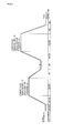
- a mirror polished silicon single crystal wafer having a diameter of 200mm and crystal orientation ⁇ 100> was thrown into a longitudinal heat treatment furnace to form a thermal oxide film having a thickness of 6000 nm by the heat treatment profile of Fig. 1 .
- Table 1 there are shown throw-in temperature Tin(°C), low temperature oxidation temperature T1(°C), lowered temperature T(°C), high temperature oxidation temperature T2(°C) and taking-out temperature Tout (°C) in this instance.
- the oxidation is performed by the pyrogenic oxidation.
- oxidation 1 oxidation time was adjusted so that a thermal oxidation film having a thickness of 1000 nm is formed.
- oxidation 2 oxidation time was adjusted so that a thermal oxidation film having a thickness of 5000 nm is additionally formed.
- the temperature-elevating rate from Tin(°C) to T1(°C) was set to 5(°C/min), and the temperature-lowering rate from Tin(°C) to T(°C) was set to 2.5(°C/min). Moreover, the temperature-elevating rate from T (°C) to T2 (°C) was set to 2(°C/min) until 900°C, was set to 1(°C/min) between 900°C and 1200(°C), and was set to 0.5(°C/min) between 1200 and 1250 (°C).
- the temperature-lowering rate from T2 (°C) to Tout(°C) was set to 0.5(°C/min.) until 1200°C, was set to 1(°C/min) between 1200 and 1100 (°C), and was set to 2(°C/min) between 1100 and Tout(°C).
- the thermal oxide film having a thickness of 6000 nm was formed thereafter to observe the slip dislocation by the X-ray topography method. As a result, at the position in contact with the wafer boat, contact trace was observed, but linear slip dislocation was not observed.
- a mirror polished silicon single crystal wafer having a diameter of 200mm and crystal orientation ⁇ 100> was thrown into a longitudinal heat treatment furnace to form a thermal oxide film having a thickness of 5500 nm by the heat treatment profile of Fig. 1 .
- Table 1 there are shown throw-in temperature Tin(°C), low temperature oxidation temperature T1(°C), lowered temperature T(°C), high temperature oxidation temperature T2(°C) and taking-out temperature Tout(°C) in this instance.
- the oxidation was performed by the pyrogenic oxidation.
- oxidation 1 oxidation time was adjusted so that a thermal oxide film having a thickness of 500 nm is formed.
- oxidation 2 oxidation time was adjusted so that a thermal oxidation film having a thickness of 5000 nm is additionally formed.
- the temperature-elevating rate from Tin(°C) to T1 (°C) was set to 5(°C/min), and the temperature-lowering rate from T1(°C) to T (°C) was set to 2.5(°C/min).
- the temperature-elevating rate from T (°C) to T2 (°C) was set to 2(°C/min) until 900°C, was set to 1(°C/min) between 900°C and 1200(°C), and was set to 0.5(°C/min) between 1200 and 1250 (°C).
- the temperature-lowering rate from T2 (°C) to Tout(°C) was set to 0.5(°C/min) until 1200°C, was set to 1(°C/min) between 1200 and 1100 (°C), and was set to 2(°C/min) between 1100 and Tout(°C).
- the thermal oxide film having a thickness of 5500 nm was formed thereafter to observe the slip dislocation by the X-ray topography method. As a result, at the position in contact with the wafer boat, contact trace was observed, but linear slip dislocation was not observed.
- a mirror polished silicon single crystal wafer having a diameter of 200 mm and crystal orientation ⁇ 100> was thrown into a longitudinal heat treatment furnace to form an oxide film having a thickness of 2500 nm by the heat treatment profile of Fig. 1 .
- the table 1 there are shown throw-in temperature Tin(°C), low temperature oxidation temperature T1(°C), lowered temperature T(°C), high temperature oxidation temperature T2 (°C) and taking-out temperature Tout(°C) in this instance.
- the oxidation is performed by the pyrogenic oxidation.
- oxidation 1 oxidation time was adjusted so that a thermal oxidation film having a thickness of 500 nm is formed.
- oxidation 2 oxidation time was adjusted so that a thermal oxidation film having a thickness of 2000 nm is additionally formed.
- the temperature-elevating rate from Tin(°C) to T1(°C) was set to 5(°C/min), and the temperature-lowering rate from T1(°C) to T (°C) was set to 2.5(°C/min). Moreover, the temperature-elevating rate from T(°C) to T2(°C) was set to 2 (°C/min) until 900°C, and was set to 1 (°C/min) between 900°C and 1200 (°C). The temperature-lowering rate from T2(°C) to Tout(°C) was set to 1(°C/min) until 1100°C, and was set to 2(°C/min) between 1100 and Tout(°C).
- the thermal oxide film having a thickness of 2500 nm was formed thereafter to observe the slip dislocation by the X-ray topography method. As a result, at the position in contact with the wafer boat, contact trace was observed, but linear slip dislocation was not observed.
- thermal oxide film thicknesses in Examples 1-3 are shown in Table 2.
- Oxidation (1) Oxidation (2) Total oxide film thickness d1 (nm) d2 (nm)
- Example 1 1000 5000 6000 nm
- Example 2 500 5000 5500 nm
- Example 3 500 2000 2500 nm
- a thermal oxide film having a thickness of 6000 nm was formed under the same condition as that of the example 1 except for the fact that the wafer is once taken out toward the outside of the heat treatment furnace after temperature lowering down to T(°C).
- the thermal oxide film having a thickness of 6000 nm was formed thereafter to observe the slip dislocation by the X-ray topography method. As a result, at the position in contact with the wafer boat, contact trace was observed, but linear slip dislocation was not observed.
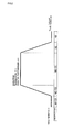
- a mirror polished silicon single crystal wafer having a diameter of 200 mm and crystal orientation ⁇ 100> was thrown into a longitudinal heat treatment furnace to form an oxide film having a thickness of 6000 nm by the heat treatment profile of Fig. 2 .
- the table 3 there are shown throw-in temperature Tin(°C), oxidation temperature T11(°C), and taking out temperature Tout(°C) in this instance.
- the temperature-elevating rate and the temperature-lowering rate were set to the same condition as those at the time of the high temperature oxidation of Example 1.
- the thermal oxide film having a thickness of 6000 nm was formed thereafter to observe the slip dislocation by the X-ray topography method. As a result, a strong linear slip dislocation having, as base point, contact trace with respect to the wafer boat was observed as crossing mark.
- a mirror polished silicon single crystal wafer having a diameter of 200 mm and crystal orientation ⁇ 100> was thrown into a longitudinal heat treatment furnace to form an oxide film having a thickness of 2500 nm by the heat treatment profile of Fig. 2 .
- Table 3 there are shown throw-in temperature Tin(°C), oxidation temperature T11(°C) and taking-out temperature Tout(°C) in this instance.
- the temperature-elevating rate and temperature-lowering rate were set to the same condition as those at the time of the high temperature oxidation of Example 3.
- the thermal oxide film having a thickness of 2500 nm was formed thereafter to observe a slip dislocation by the X-ray topography.
- a linear slip dislocation having, as base point, contact trace with respect to wafer boat was observed as crossing mark.
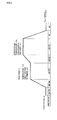
- a mirror polished silicon single crystal wafer having a diameter of 200 mm and crystal orientation ⁇ 100> was thrown into a longitudinal heat treatment furnace to form a thermal oxide film having a thickness of 6000 nm by the heat treatment profile, as described in Fig. 3 , having double-stage heat treatment in which temperature elevating is performed without temperature lowering between heat treatments of the preceding stage and the succeeding stage.
- Table 5 there are shown throw-in temperature Tin(°C), oxidation temperatures T11, T12 (°C) and taking-out temperature Tout(°C).
- the oxidation was performed by the pyrogenic oxidation.
- oxidation 1 oxidation time was adjusted so that a thermal oxide film having a thickness 1000 nm is formed.
- oxidation 2 In the case of the high temperature oxidation (oxidation 2), oxidation time was adjusted so that a thermal oxide film having a thickness 5000 nm is additionally formed. In addition, the temperature-elevating rate and the temperature-lowering rate were set to the same conditions as those of Example 1.
- a thermal oxide film having a thickness of 6000 nm was formed thereafter to observe slip dislocation by the X-ray topography method.
- a strong linear slip dislocation (weak (short) as compared to Comparative Example 1) having, as base point, contact trace with respect to wafer boat was observed as crossing mark.
Landscapes
- Formation Of Insulating Films (AREA)
- Crystals, And After-Treatments Of Crystals (AREA)
Abstract
Description
- The present invention relates to a thermal oxide film formation method for suppressing slip dislocation, etc. taking place when thermal oxide film is formed on a silicon single crystal wafer.
- Hitherto, in order to form a thermal oxide film on the surface of a silicon single crystal wafer, e.g., silicon single crystal wafer is mounted on a heat treatment jig (frequently referred to as wafer boat) made of heat resistant material (e.g., quartz or SiC) to set such a jig within a tube for heat treatment furnace to perform heat treatment under oxidizing atmosphere.
Control of film thickness of the thermal oxide film formed in this way is performed after subjected to calculation by the kind of the heat treatment atmosphere, the heat treatment temperature and/or heat treatment time. - In regard to film thickness of thermal oxide film to be formed on the surface of the silicon single crystal wafer, although depending upon the purpose, in the case of fabricating a bonded SOI wafer including a thick buried oxide film layer (BOX layer) as described in the
Patent Literature 1, a thick thermal oxide film is formed on at least one of two silicon single crystal wafers to be bonded and a bonding process is performed. - For the purpose of forming such a thick oxide film, high temperature/long time heat treatment is performed under the atmosphere including water vapor such as wet O2 oxidation or pyrogenic oxidation, etc. as the heat treatment atmosphere where oxidation rate is high.
-
- Patent Literature 1:Japanese Unexamined Patent Publication (Kokai) No.
2008-277702 - Particularly, in forming a thick thermal oxide film, when high temperature/long time heat treatment is performed under the atmosphere including water vapor, the thermal oxide film formed on the surface of the silicon single crystal wafer is stuck onto a wafer boat. For this reason, there was the problem that slip dislocation and/or crack may take place at the part thereof.
- The present invention has been made in view of the above-described problems, and aims at providing a method of forming a thermal oxide film of preventing sticking onto a wafer boat taking place particularly in forming s thick oxide film to have ability to suppress occurrence of slip dislocation and/or crack of a silicon single crystal wafer during formation of the thermal oxide film.
- To attain the above-mentioned problems, the present invention provides a method of forming a thermal oxide film on a silicon single crystal wafer, at least comprising: throwing the silicon single crystal wafer into a heat treatment furnace; elevating temperature of the heat treatment furnace up to a temperature T1 where a thermal oxide film is formed to form a thermal oxide film having a thickness d1; subsequently lowering the temperature of the heat treatment furnace down to a temperature lower than the temperature T1; and thereafter elevating the temperature of the heat treatment furnace up to a temperature T2 higher than the temperature T1 to additionally form a thermal oxide film having a thickness d2 thicker than the thickness d1.
- By forming the thermal oxide film in this way, warp phenomenon of wafer takes place resulting from a temperature difference between a wafer outer peripheral part and a central part occurring at the time of lowering temperature, and therefore a position in contact with a wafer boat for holding the wafer changes. For this reason, it is possible to prevent that the wafer is stuck onto the wafer boat by the thermal oxide film. Moreover, the thermal oxide film formed during oxidation at the temperature T1 of the preceding stage has the effect of the protective film in high temperature oxidation performed at the temperature T2 of the succeeding stage. Further, a thick oxide film is additionally formed by high temperature oxidation of the succeeding stage, while suppressing occurrence of the slip dislocation and/or crack in the state where the contact position is changed and the thermal oxide film as the protective film is formed at the preceding stage. Therefore, it is possible to efficiently form satisfactory thick thermal oxide film.
- At this time, it is preferable that the temperature of the heat treatment furnace is elevated up to the temperature T2 higher than the temperature T1 without taking out the silicon single crystal wafer from the heat treatment furnace to additionally form a thermal oxide film having the thickness d2 thicker than the thickness d1 after the temperature of the heat treatment furnace is lowered down to the temperature lower than the temperature T1.
The thermal oxide film is additionally formed as described above, thereby making it possible to additionally form the thermal oxide film continuously within the heat treatment furnace. Such a process is efficient. - At this time, it is preferable that the temperature T1 is set to a temperature lower than 1200°C, and the temperature T2 is set to a temperature of 1200°C or more.
As described above, the temperature T1 is set to a temperature lower than 1200°C, thereby making it possible to form a thermal oxide film while effectively preventing occurrence of slip dislocation by the low temperature oxidation of the preceding stage. Moreover, the temperature T2 is set to a temperature of 1200°C or more, thereby making it possible to efficiently form thick thermal oxide film by the high temperature oxidation of the succeeding stage at a sufficient oxidation rate. - At this time, it is preferable that when the temperature of the heat treatment furnace is lowered down to the temperature lower than the temperature T1, the temperature of the heat treatment furnace is lowered down to a temperature lower than the temperature T1 by 200°C or more.
As described above, the temperature of the heat treatment furnace is lowered down to the temperature lower than the temperature T1 by 200°C or more, thereby making it possible to allow warp phenomenon of the wafer at time of lowering temperature to sufficiently take place to change the position in contact with the wafer boat thus to effectively prevent sticking. - At this time, it is preferable that when the temperature of the heat treatment furnace is lowered down to the temperature lower than the temperature T1, the temperature of the heat treatment furnace is lowered down to a temperature equal to or less than a throw-in temperature when the silicon single crystal wafer is thrown into the heat treatment furnace.
As described above, the temperature of the heat treatment furnace is lowered down to a temperature equal to or less than a throw-in temperature when the silicon single crystal wafer is thrown into the heat treatment furnace, thereby making it possible to allow warp phenomenon of the wafer at the time of lowering temperature to sufficiently take place to change the position in contact with the wafer boat to securely prevent sticking. - At this time, a film thickness obtained by totalizing the thickness d1 and the thickness d2 may be 2500 nm or more.
Also in forming such a thick thermal oxide film, in accordance with the method according to the present invention, it is possible to prevent occurrence of slip dislocation thus to perform satisfactory formation of the thermal oxide film. - At this time, it is preferable that the thickness d1 is 500 nm or more.
As described above, the thickness d1 is 500 nm or more so that the thermal oxide film thus formed functions as a satisfactory protective film in high temperature oxidation of the succeeding stage to securely prevent occurrence of the slip dislocation. - At this time, it is preferable that after the thermal oxide film having the thickness d2 is additionally formed, further additional formation of a thermal oxide film by lowering the temperature of the heat treatment furnace down to a temperature lower than the temperature T1 and thereafter elevating the temperature of the heat treatment furnace up to a temperature higher than the temperature T1 is repeated one or more times.
The thermal oxide film is additionally formed as described above, thereby making it possible to securely prevent sticking onto the wafer boat particularly in forming a thick thermal oxide film. - As described above, in accordance with the present invention, it is possible to efficiently perform thermal oxide film formation while suppressing occurrence of slip dislocation and/or crack particularly also in forming a thick thermal oxide film.
-
-
Fig. 1 is a view showing temperature and atmospheric gas within a heat treatment furnace in an example, -
Fig. 2 is view showing temperature and atmospheric gas within a heat treatment furnace in comparative examples 1, 2, and -
Fig. 3 is a view showing temperature and atmospheric gas within a heat treatment furnace in a comparative example 3. - While the present invention will now be described in detail with reference to the drawings as an example of preferred embodiments, the present invention is not limited to such an implementation.
- In the present invention, a silicon single crystal wafer is first thrown into, e.g., a longitudinal heat treatment furnace.
In this instance, wafers are filled into a wafer boat having supporting parts for mounting a plurality of wafers thereon to perform loading the wafer boat into a tube of the heat treatment furnace to thereby throw them thereinto. As temperature (throw-in temperature) within the heat treatment furnace at this time, a heater is set so that there is provided, e.g., temperature of about 500°C - Next, the temperature of the heat treatment furnace is elevated up to the temperature T1 where a thermal oxide film is formed to hold such temperature to thereby form a thermal oxide film having thickness d1.
At this time, as long as the temperature of the heat treatment furnace is a temperature such that thermal oxide film can be formed on a silicon single crystal wafer, the temperature T1 where the thermal oxide film is formed is not particularly limited. In this case, when the temperature of the heat treatment furnace is a temperature higher than 600°C, a thermal oxide film having a certain thickness is formed, but it is preferable that, e.g., the temperature T1 is a temperature lower than 1200°C. When the temperature of the heat treatment furnace is a temperature lower than 1200°C, it is possible to sufficiently suppress occurrence of the slip dislocation during formation of the thermal oxide film. - The thickness d1 of the thermal oxide film to be formed at this time is not particularly limited, but e.g., a thickness of 500 nm or more is preferable.
The thermal oxide film having such a thickness is formed, whereby the thermal oxide film has a thickness to a degree such that the thermal oxide film sufficiently functions as a protective film in high temperature oxidation of the succeeding stage, thus making it possible to sufficiently suppress occurrence of the slip dislocation. - Next, the temperature of the heat treatment furnace is lowered down to a temperature lower than the temperature T1.
In this way, the temperature of the heat treatment furnace is lowered so that a temperature difference takes place between the outer peripheral part of the wafer and the central part thereof. As a result, warp phenomenon takes place at the wafer resulting from the temperature difference. Thus, the position in contact with the wafer boat changes. For this reason, it can be prevented that the wafer may be stuck onto the wafer boat by the thermal oxide film formed. - In this instance, it is preferable that the temperature of the heat treatment is lowered down to a temperature lower than the temperature T1 by 200°C or more. Moreover, it is more preferable that the temperature of the heat treatment furnace is lowered down to a temperature equal to or less than a throw-in temperature when the silicon single crystal wafer is thrown into the heat treatment furnace.
When the temperature of the heat treatment furnace is lowered down to such a temperature, warp phenomenon of the wafer is caused to sufficiently take place, thereby making it possible to securely attain sticking prevention based on change of the position in contact with the wafer boat. - Next, the temperature of the heat treatment furnace is elevated up to a temperature T2 higher than the temperature T1 to additionally form a thermal oxide film having thickness d2 thicker than the thickness d1.
In this way, in the high temperature oxidation process of the succeeding stage, because the thermal oxide film is already formed at the low temperature oxidation process of the preceding stage, this thermal oxide film functions as a protective film so that slip dislocation is difficult to occur even at a high temperature. Moreover, when a thermal oxide film having thickness d2 thicker than that of the low temperature oxidation of the preceding stage in high temperature oxidation, since the oxidation rate is high due to high temperature, it is possible to efficiently and additionally form thick thermal oxide film. - The temperature T2 at this time may be a temperature higher than the temperature T1, but is not particularly limited. In this case, for example, it is preferable that the temperature T2 is 1200°C or more.
When the temperature T2 is 1200°C or more, since the oxidation rate is sufficiently high, such a process is efficient. Moreover, even when the temperature T2 is such a high temperature, since the thermal oxide film is formed by the low temperature oxidation of the preceding stage in the present invention, such thermal oxide film functions as a protective film so that slip dislocation is difficult to take place. - Moreover, while a wafer can be taken out toward the outside of the heat treatment furnace before the temperature of the heat treatment furnace is elevated up to the temperature T2 after the temperature of the heat treatment furnace is lowered, it is preferable that if the throughput of the oxidation process is taken into account, the temperature of the heat treatment furnace is elevated up to the temperature T2 without taking out the wafer toward the outside of the heat treatment furnace to continuously perform formation of the oxide film after the temperature of the heat treatment furnace is lowered.
- Such temperature elevation, temperature lowering and temperature holding within the heat treatment furnace may be performed by controlling heater output. Moreover, temperature-elevating rate and temperature-lowering rate are not particularly limited.
Further, as long as the atmosphere in formation of a thermal oxide film is oxidizing atmosphere where the oxide film is formed, the atmosphere is not also particularly limited, and e.g., wet O2 oxidation and/or pyrogenic oxidation, etc. may be performed under the atmosphere including vapor water. - According to the thermal oxide film formation method of the present invention as described above, occurrence of slip dislocation and/or crack is prevented also in forming a thick thermal oxide film having thickness of 2500 nm or more, otherwise 5000 nm or more where slip dislocation, etc. is apt to particularly take place, and thus a satisfactory thermal oxide film can be formed.
- Moreover, the thermal oxide film having the thickness d2 is additionally formed in a manner as described above, further additional formation of a thermal oxide film by lowering the temperature of the heat treatment furnace down to a temperature lower than the temperature T1 and thereafter elevating the temperature of the heat treatment furnace up to a temperature higher than the temperature T1 is repeated one or more times.
Particularly in the case of forming a thick thermal oxide film, etc., temperature lowering and temperature elevation of the present invention may be repeated further one or more times in this way to thereby prevent sticking onto the wafer boat, thus making it possible securely prevent slip dislocation and/or crack. - It is to be noted that the oxide film formation method according to the present invention may be also applied to a bonded SOI wafer made by bonding two ordinary silicon single crystal wafers through the oxide film, and to a SOI wafer fabricated through high temperature heat treatment after oxygen ions are implanted into an ordinary silicon single crystal wafer, in addition to ordinary silicon single crystal wafer comprised of only silicon single crystal. Accordingly, "silicon single crystal wafer" in the present invention may include these SOI wafers.
- While the present invention will be described in more concrete manner by making reference to the examples and the comparative examples, the present invention is not limited to these examples.
- A mirror polished silicon single crystal wafer having a diameter of 200mm and crystal orientation <100> was thrown into a longitudinal heat treatment furnace to form a thermal oxide film having a thickness of 6000 nm by the heat treatment profile of
Fig. 1 . In the Table 1, there are shown throw-in temperature Tin(°C), low temperature oxidation temperature T1(°C), lowered temperature T(°C), high temperature oxidation temperature T2(°C) and taking-out temperature Tout (°C) in this instance. - The oxidation is performed by the pyrogenic oxidation. In the case of the low temperature oxidation (oxidation 1), oxidation time was adjusted so that a thermal oxidation film having a thickness of 1000 nm is formed. In the case of the high temperature oxidation (oxidation 2), oxidation time was adjusted so that a thermal oxidation film having a thickness of 5000 nm is additionally formed.
- The temperature-elevating rate from Tin(°C) to T1(°C) was set to 5(°C/min), and the temperature-lowering rate from Tin(°C) to T(°C) was set to 2.5(°C/min).
Moreover, the temperature-elevating rate from T (°C) to T2 (°C) was set to 2(°C/min) until 900°C, was set to 1(°C/min) between 900°C and 1200(°C), and was set to 0.5(°C/min) between 1200 and 1250 (°C). The temperature-lowering rate from T2 (°C) to Tout(°C) was set to 0.5(°C/min.) until 1200°C, was set to 1(°C/min) between 1200 and 1100 (°C), and was set to 2(°C/min) between 1100 and Tout(°C). - The thermal oxide film having a thickness of 6000 nm was formed thereafter to observe the slip dislocation by the X-ray topography method. As a result, at the position in contact with the wafer boat, contact trace was observed, but linear slip dislocation was not observed.
- A mirror polished silicon single crystal wafer having a diameter of 200mm and crystal orientation <100> was thrown into a longitudinal heat treatment furnace to form a thermal oxide film having a thickness of 5500 nm by the heat treatment profile of
Fig. 1 . In the Table 1, there are shown throw-in temperature Tin(°C), low temperature oxidation temperature T1(°C), lowered temperature T(°C), high temperature oxidation temperature T2(°C) and taking-out temperature Tout(°C) in this instance. - The oxidation was performed by the pyrogenic oxidation. In the case of the low temperature oxidation (oxidation 1), oxidation time was adjusted so that a thermal oxide film having a thickness of 500 nm is formed. In the case of the high temperature oxidation (oxidation 2), oxidation time was adjusted so that a thermal oxidation film having a thickness of 5000 nm is additionally formed.
- The temperature-elevating rate from Tin(°C) to T1 (°C) was set to 5(°C/min), and the temperature-lowering rate from T1(°C) to T (°C) was set to 2.5(°C/min). Moreover, the temperature-elevating rate from T (°C) to T2 (°C) was set to 2(°C/min) until 900°C, was set to 1(°C/min) between 900°C and 1200(°C), and was set to 0.5(°C/min) between 1200 and 1250 (°C). The temperature-lowering rate from T2 (°C) to Tout(°C) was set to 0.5(°C/min) until 1200°C, was set to 1(°C/min) between 1200 and 1100 (°C), and was set to 2(°C/min) between 1100 and Tout(°C).
- The thermal oxide film having a thickness of 5500 nm was formed thereafter to observe the slip dislocation by the X-ray topography method. As a result, at the position in contact with the wafer boat, contact trace was observed, but linear slip dislocation was not observed.
- A mirror polished silicon single crystal wafer having a diameter of 200 mm and crystal orientation <100> was thrown into a longitudinal heat treatment furnace to form an oxide film having a thickness of 2500 nm by the heat treatment profile of
Fig. 1 . In the table 1, there are shown throw-in temperature Tin(°C), low temperature oxidation temperature T1(°C), lowered temperature T(°C), high temperature oxidation temperature T2 (°C) and taking-out temperature Tout(°C) in this instance. - The oxidation is performed by the pyrogenic oxidation. In the case of the low temperature oxidation (oxidation 1), oxidation time was adjusted so that a thermal oxidation film having a thickness of 500 nm is formed. In the case of the high temperature oxidation (oxidation 2), oxidation time was adjusted so that a thermal oxidation film having a thickness of 2000 nm is additionally formed.
- The temperature-elevating rate from Tin(°C) to T1(°C) was set to 5(°C/min), and the temperature-lowering rate from T1(°C) to T (°C) was set to 2.5(°C/min).
Moreover, the temperature-elevating rate from T(°C) to T2(°C) was set to 2 (°C/min) until 900°C, and was set to 1 (°C/min) between 900°C and 1200 (°C). The temperature-lowering rate from T2(°C) to Tout(°C) was set to 1(°C/min) until 1100°C, and was set to 2(°C/min) between 1100 and Tout(°C). - The thermal oxide film having a thickness of 2500 nm was formed thereafter to observe the slip dislocation by the X-ray topography method. As a result, at the position in contact with the wafer boat, contact trace was observed, but linear slip dislocation was not observed.
- The temperatures at the time of forming thermal oxide film in Examples 1-3 are shown in Table 1, and the thermal oxide film thicknesses in Examples 1-3 are shown in Table 2.
-
[Table 1] Tin(°C) T1(°C) T(°C) T2(°C) Tout(°C) Example 1 500 1050 500 1250 500 Example 2 600 1000 800 1250 600 Example 3 500 1000 500 1200 500 -
[Table 2] Oxidation (1) Oxidation (2) Total oxide film thickness d1 (nm) d2 (nm) Example 1 1000 5000 6000 nm Example 2 500 5000 5500 nm Example 3 500 2000 2500 nm - A thermal oxide film having a thickness of 6000 nm was formed under the same condition as that of the example 1 except for the fact that the wafer is once taken out toward the outside of the heat treatment furnace after temperature lowering down to T(°C).
The thermal oxide film having a thickness of 6000 nm was formed thereafter to observe the slip dislocation by the X-ray topography method. As a result, at the position in contact with the wafer boat, contact trace was observed, but linear slip dislocation was not observed. - A mirror polished silicon single crystal wafer having a diameter of 200 mm and crystal orientation <100> was thrown into a longitudinal heat treatment furnace to form an oxide film having a thickness of 6000 nm by the heat treatment profile of
Fig. 2 . In the table 3, there are shown throw-in temperature Tin(°C), oxidation temperature T11(°C), and taking out temperature Tout(°C) in this instance.
In addition, the temperature-elevating rate and the temperature-lowering rate were set to the same condition as those at the time of the high temperature oxidation of Example 1. - The thermal oxide film having a thickness of 6000 nm was formed thereafter to observe the slip dislocation by the X-ray topography method. As a result, a strong linear slip dislocation having, as base point, contact trace with respect to the wafer boat was observed as crossing mark.
- A mirror polished silicon single crystal wafer having a diameter of 200 mm and crystal orientation <100> was thrown into a longitudinal heat treatment furnace to form an oxide film having a thickness of 2500 nm by the heat treatment profile of
Fig. 2 . In Table 3, there are shown throw-in temperature Tin(°C), oxidation temperature T11(°C) and taking-out temperature Tout(°C) in this instance.
In addition, the temperature-elevating rate and temperature-lowering rate were set to the same condition as those at the time of the high temperature oxidation of Example 3. - The thermal oxide film having a thickness of 2500 nm was formed thereafter to observe a slip dislocation by the X-ray topography. As a result, a linear slip dislocation having, as base point, contact trace with respect to wafer boat was observed as crossing mark.
- The temperatures at the time of forming thermal oxide films in Comparative Examples 1, 2 are shown in the Table 3, and the thermal oxide film thicknesses in Comparative Examples 1, 2 are shown in Table 4.
-
[Table 3] Tin(°C) T11(°C) Tout(°C) Comparative Example 1 500 1250 500 Comparative Example 2 500 1200 500 -
[Table 4] Oxidation d11(nm) Comparative Example 1 6000 Comparative Example 2 2500 - A mirror polished silicon single crystal wafer having a diameter of 200 mm and crystal orientation <100> was thrown into a longitudinal heat treatment furnace to form a thermal oxide film having a thickness of 6000 nm by the heat treatment profile, as described in
Fig. 3 , having double-stage heat treatment in which temperature elevating is performed without temperature lowering between heat treatments of the preceding stage and the succeeding stage. In Table 5, there are shown throw-in temperature Tin(°C), oxidation temperatures T11, T12 (°C) and taking-out temperature Tout(°C). The oxidation was performed by the pyrogenic oxidation. In the case of low temperature oxidation (oxidation 1), oxidation time was adjusted so that a thermal oxide film having a thickness 1000 nm is formed. In the case of the high temperature oxidation (oxidation 2), oxidation time was adjusted so that a thermal oxide film having a thickness 5000 nm is additionally formed.
In addition, the temperature-elevating rate and the temperature-lowering rate were set to the same conditions as those of Example 1. - A thermal oxide film having a thickness of 6000 nm was formed thereafter to observe slip dislocation by the X-ray topography method. As a result, a strong linear slip dislocation (weak (short) as compared to Comparative Example 1) having, as base point, contact trace with respect to wafer boat was observed as crossing mark.
- The temperatures at the time of forming thermal oxide film in Comparative Example 3 are shown in Table 5, and the thermal oxide film thicknesses in Comparative Example 3 are illustrated in Table 6.
-
[Table 5] Tin(°C) T11(°C) T12(°C) Tout(°C) Comparative Example 3 500 1050 1250 500 -
[Table 6] Oxidation (1) Oxidation (2) Total oxide film thickness d11 (nm) d12 (nm) Comparative Example 3 1000 5000 6000 nm - It is to be noted that the present invention is not restricted to the foregoing embodiment. The foregoing embodiment is just an exemplification, and any examples that have substantially the same configuration and demonstrate the same functions and effects as the technical concept described in claims of the present invention are included in the technical scope of the present invention.
Claims (8)
- A method of forming a thermal oxide film on a silicon single crystal wafer, at least comprising:throwing the silicon single crystal wafer into a heat treatment furnace;elevating temperature of the heat treatment furnace up to a temperature T1 where a thermal oxide film is formed to form a thermal oxide film having a thickness d1;subsequently lowering the temperature of the heat treatment furnace down to a temperature lower than the temperature T1; and thereafterelevating the temperature of the heat treatment furnace up to a temperature T2 higher than the temperature T1 to additionally form a thermal oxide film having a thickness d2 thicker than the thickness d1.
- The method of forming a thermal oxide film on a silicon single crystal wafer according to claim 1, wherein
the temperature of the heat treatment furnace is elevated up to the temperature T2 higher than the temperature T1 without taking out the silicon single crystal wafer from the heat treatment furnace to additionally form a thermal oxide film having the thickness d2 thicker than the thickness d1 after the temperature of the heat treatment furnace is lowered down to the temperature lower than the temperature T1. - The method of forming a thermal oxide film on a silicon single crystal wafer according to claim 1 or 2,
wherein the temperature T1 is set to a temperature lower than 1200°C, and the temperature T2 is set to a temperature of 1200°C or more. - The method of forming a thermal oxide film on a silicon single crystal wafer according to any one of claims 1 to 3,
wherein when the temperature of the heat treatment furnace is lowered down to the temperature lower than the temperature T1, the temperature of the heat treatment furnace is lowered down to a temperature lower than the temperature T1 by 200°C or more. - The method of forming a thermal oxide film on a silicon single crystal wafer according to any one of claims 1 to 4,
wherein when the temperature of the heat treatment furnace is lowered down to the temperature lower than the temperature T1, the temperature of the heat treatment furnace is lowered down to a temperature equal to or less than a throw-in temperature when the silicon single crystal wafer is thrown into the heat treatment furnace. - The method of forming a thermal oxide film on a silicon single crystal wafer according to any one of claims 1 to 5,
wherein a film thickness obtained by totalizing the thickness d1 and the thickness d2 is 2500 nm or more. - The method of forming a thermal oxide film on a silicon single crystal wafer according to any one of claims 1 to 6,
wherein the thickness d1 is 500 nm or more. - The method of forming a thermal oxide film on a silicon single crystal wafer according to any one of claims 1 to 7,
wherein after the thermal oxide film having the thickness d2 is additionally formed, further additional formation of a thermal oxide film by lowering the temperature of the heat treatment furnace down to a temperature lower than the temperature T1 and thereafter elevating the temperature of the heat treatment furnace up to a temperature higher than the temperature T1 is repeated one or more times.
Applications Claiming Priority (2)
| Application Number | Priority Date | Filing Date | Title |
|---|---|---|---|
| JP2010251775A JP5479304B2 (en) | 2010-11-10 | 2010-11-10 | Method for forming thermal oxide film on silicon single crystal wafer |
| PCT/JP2011/005626 WO2012063402A1 (en) | 2010-11-10 | 2011-10-06 | Method for forming thermal oxide film of monocrystalline silicon wafer |
Publications (3)
| Publication Number | Publication Date |
|---|---|
| EP2639819A1 true EP2639819A1 (en) | 2013-09-18 |
| EP2639819A4 EP2639819A4 (en) | 2014-04-02 |
| EP2639819B1 EP2639819B1 (en) | 2017-01-04 |
Family
ID=46050574
Family Applications (1)
| Application Number | Title | Priority Date | Filing Date |
|---|---|---|---|
| EP11839425.3A Active EP2639819B1 (en) | 2010-11-10 | 2011-10-06 | Method for forming thermal oxide film of monocrystalline silicon wafer |
Country Status (6)
| Country | Link |
|---|---|
| US (1) | US9171737B2 (en) |
| EP (1) | EP2639819B1 (en) |
| JP (1) | JP5479304B2 (en) |
| KR (1) | KR101725777B1 (en) |
| CN (1) | CN103262222B (en) |
| WO (1) | WO2012063402A1 (en) |
Families Citing this family (3)
| Publication number | Priority date | Publication date | Assignee | Title |
|---|---|---|---|---|
| JP5780234B2 (en) * | 2012-12-14 | 2015-09-16 | 信越半導体株式会社 | Manufacturing method of SOI wafer |
| CN105355551B (en) * | 2015-11-12 | 2018-05-15 | 扬州杰利半导体有限公司 | A kind of wafer passivation technique |
| CN117096012B (en) * | 2023-08-22 | 2024-03-26 | 中环领先半导体科技股份有限公司 | Oxide film, silicon wafer and preparation method thereof |
Family Cites Families (34)
| Publication number | Priority date | Publication date | Assignee | Title |
|---|---|---|---|---|
| US4494303A (en) * | 1983-03-31 | 1985-01-22 | At&T Bell Laboratories | Method of making dielectrically isolated silicon devices |
| JPH02303131A (en) * | 1989-05-18 | 1990-12-17 | Oki Electric Ind Co Ltd | Insulating film formation method |
| US5244843A (en) * | 1991-12-17 | 1993-09-14 | Intel Corporation | Process for forming a thin oxide layer |
| US5648282A (en) * | 1992-06-26 | 1997-07-15 | Matsushita Electronics Corporation | Autodoping prevention and oxide layer formation apparatus |
| JPH06112451A (en) * | 1992-09-29 | 1994-04-22 | Nagano Denshi Kogyo Kk | Method for manufacturing SOI substrate |
| JP3105770B2 (en) * | 1995-09-29 | 2000-11-06 | 日本電気株式会社 | Method for manufacturing semiconductor device |
| US5738909A (en) * | 1996-01-10 | 1998-04-14 | Micron Technology, Inc. | Method of forming high-integrity ultrathin oxides |
| US5962854A (en) * | 1996-06-12 | 1999-10-05 | Ishizuka Electronics Corporation | Infrared sensor and infrared detector |
| JP3981426B2 (en) * | 1996-07-12 | 2007-09-26 | シャープ株式会社 | Method for forming gate insulating film |
| US6797323B1 (en) * | 1996-11-29 | 2004-09-28 | Sony Corporation | Method of forming silicon oxide layer |
| JPH11186255A (en) * | 1996-11-29 | 1999-07-09 | Sony Corp | Method of forming silicon oxide film |
| US5851892A (en) * | 1997-05-07 | 1998-12-22 | Cypress Semiconductor Corp. | Fabrication sequence employing an oxide formed with minimized inducted charge and/or maximized breakdown voltage |
| US6207591B1 (en) * | 1997-11-14 | 2001-03-27 | Kabushiki Kaisha Toshiba | Method and equipment for manufacturing semiconductor device |
| JPH11288893A (en) * | 1998-04-03 | 1999-10-19 | Nec Corp | Semiconductor manufacturing apparatus and semiconductor device manufacturing method |
| US6541394B1 (en) * | 1999-01-12 | 2003-04-01 | Agere Systems Guardian Corp. | Method of making a graded grown, high quality oxide layer for a semiconductor device |
| US6281141B1 (en) * | 1999-02-08 | 2001-08-28 | Steag Rtp Systems, Inc. | Process for forming thin dielectric layers in semiconductor devices |
| JP2000232222A (en) * | 1999-02-10 | 2000-08-22 | Nec Corp | Method for manufacturing semiconductor device |
| US6235651B1 (en) * | 1999-09-14 | 2001-05-22 | Infineon Technologies North America | Process for improving the thickness uniformity of a thin layer in semiconductor wafer fabrication |
| US6437375B1 (en) * | 2000-06-05 | 2002-08-20 | Micron Technology, Inc. | PD-SOI substrate with suppressed floating body effect and method for its fabrication |
| JP4914536B2 (en) * | 2001-02-28 | 2012-04-11 | 東京エレクトロン株式会社 | Oxide film formation method |
| US6455382B1 (en) * | 2001-05-03 | 2002-09-24 | Taiwan Semiconductor Manufacturing Co., Ltd. | Multi-step method for forming sacrificial silicon oxide layer |
| US6602799B2 (en) * | 2001-09-17 | 2003-08-05 | Taiwan Semiconductor Manufacturing Co., Ltd | Method of forming a uniform ultra-thin gate oxide layer |
| JP3744889B2 (en) * | 2002-06-03 | 2006-02-15 | 三洋電機株式会社 | Manufacturing method of semiconductor device |
| US6890831B2 (en) | 2002-06-03 | 2005-05-10 | Sanyo Electric Co., Ltd. | Method of fabricating semiconductor device |
| JP2004253777A (en) * | 2003-01-31 | 2004-09-09 | Nec Electronics Corp | Semiconductor device and method of manufacturing semiconductor device |
| US7576369B2 (en) * | 2005-10-25 | 2009-08-18 | Udt Sensors, Inc. | Deep diffused thin photodiodes |
| KR20040096377A (en) * | 2003-05-09 | 2004-11-16 | 삼성전자주식회사 | Method of formimg oxide layer and oxynitride layer |
| US7071127B2 (en) * | 2003-05-20 | 2006-07-04 | Promos Technologies, Inc. | Methods for improving quality of semiconductor oxide composition formed from halogen-containing precursor |
| JP4329655B2 (en) * | 2004-09-10 | 2009-09-09 | セイコーエプソン株式会社 | Semiconductor device manufacturing method and semiconductor manufacturing apparatus. |
| JP4427489B2 (en) * | 2005-06-13 | 2010-03-10 | 株式会社東芝 | Manufacturing method of semiconductor device |
| JP2007053227A (en) * | 2005-08-18 | 2007-03-01 | Matsushita Electric Ind Co Ltd | Semiconductor device and manufacturing method thereof |
| JP5280015B2 (en) * | 2007-05-07 | 2013-09-04 | 信越半導体株式会社 | Manufacturing method of SOI substrate |
| JP2010140947A (en) * | 2008-12-09 | 2010-06-24 | Hitachi Kokusai Electric Inc | Manufacturing method for semiconductor device, and substrate processing apparatus |
| JP5166297B2 (en) * | 2009-01-21 | 2013-03-21 | 東京エレクトロン株式会社 | Method for forming silicon oxide film, method for manufacturing semiconductor memory device, and computer-readable storage medium |
-
2010
- 2010-11-10 JP JP2010251775A patent/JP5479304B2/en active Active
-
2011
- 2011-10-06 US US13/824,028 patent/US9171737B2/en active Active
- 2011-10-06 CN CN201180054251.2A patent/CN103262222B/en active Active
- 2011-10-06 WO PCT/JP2011/005626 patent/WO2012063402A1/en not_active Ceased
- 2011-10-06 KR KR1020137010398A patent/KR101725777B1/en active Active
- 2011-10-06 EP EP11839425.3A patent/EP2639819B1/en active Active
Also Published As
| Publication number | Publication date |
|---|---|
| US20130178071A1 (en) | 2013-07-11 |
| US9171737B2 (en) | 2015-10-27 |
| CN103262222A (en) | 2013-08-21 |
| JP5479304B2 (en) | 2014-04-23 |
| KR101725777B1 (en) | 2017-04-11 |
| JP2012104651A (en) | 2012-05-31 |
| KR20140015263A (en) | 2014-02-06 |
| WO2012063402A1 (en) | 2012-05-18 |
| CN103262222B (en) | 2016-03-30 |
| EP2639819A4 (en) | 2014-04-02 |
| EP2639819B1 (en) | 2017-01-04 |
Similar Documents
| Publication | Publication Date | Title |
|---|---|---|
| EP3573088A1 (en) | Composite substrate and method for manufacturing composite substrate | |
| CN100418194C (en) | Manufacturing method of SOI wafer and SOI wafer | |
| JP2016072450A (en) | Bonded substrate, manufacturing method thereof, and supporting substrate for bonding | |
| CN101615577A (en) | Epitaxial wafer and manufacturing method thereof | |
| KR101120396B1 (en) | Epitaxial wafer and method of producing same | |
| CN104885190A (en) | Manufacturing method of SOI wafer | |
| JP6288323B2 (en) | Method for producing thermally oxidized heterogeneous composite substrate | |
| EP2639819B1 (en) | Method for forming thermal oxide film of monocrystalline silicon wafer | |
| JP5273150B2 (en) | Manufacturing method of silicon epitaxial wafer | |
| KR20120024970A (en) | Method for heat treating silicon wafer | |
| KR101642671B1 (en) | Handle substrates of composite substrates for semiconductors, and composite substrates for semiconductors | |
| CN108701593B (en) | Heat treatment method of semiconductor wafer | |
| CN100490070C (en) | Preventive treatment process for ring of multilayer wafer | |
| US20080268621A1 (en) | Method for manufacturing compound material wafer and corresponding compound material wafer | |
| US11393772B2 (en) | Bonding method for semiconductor substrate, and bonded semiconductor substrate | |
| CN110010445B (en) | Manufacturing method of supporting substrate for bonded wafer and manufacturing method of bonded wafer | |
| JP6822375B2 (en) | Manufacturing method of silicon epitaxial wafer | |
| JP2010153488A (en) | Manufacturing method of soi wafer, and soi wafer | |
| EP4163954A1 (en) | Support substrate for bonded wafer | |
| KR100857386B1 (en) | Heat treatment method for Sanyo wafer | |
| JP2001085649A (en) | Soi wafer and fabrication method thereof | |
| JP2010040608A (en) | Method of manufacturing laminated soi wafer | |
| KR20090059251A (en) | High resistance silicon wafer manufacturing method | |
| JP2001093789A (en) | Method for manufacturing bonded soi wafer | |
| KR20090116646A (en) | Silicon wafer and its manufacturing method |
Legal Events
| Date | Code | Title | Description |
|---|---|---|---|
| PUAI | Public reference made under article 153(3) epc to a published international application that has entered the european phase |
Free format text: ORIGINAL CODE: 0009012 |
|
| 17P | Request for examination filed |
Effective date: 20130506 |
|
| AK | Designated contracting states |
Kind code of ref document: A1 Designated state(s): AL AT BE BG CH CY CZ DE DK EE ES FI FR GB GR HR HU IE IS IT LI LT LU LV MC MK MT NL NO PL PT RO RS SE SI SK SM TR |
|
| DAX | Request for extension of the european patent (deleted) | ||
| A4 | Supplementary search report drawn up and despatched |
Effective date: 20140303 |
|
| RIC1 | Information provided on ipc code assigned before grant |
Ipc: H01L 21/02 20060101ALI20140225BHEP Ipc: H01L 21/316 20060101AFI20140225BHEP |
|
| RAP1 | Party data changed (applicant data changed or rights of an application transferred) |
Owner name: SHIN-ETSU HANDOTAI CO., LTD. |
|
| GRAP | Despatch of communication of intention to grant a patent |
Free format text: ORIGINAL CODE: EPIDOSNIGR1 |
|
| INTG | Intention to grant announced |
Effective date: 20160818 |
|
| GRAS | Grant fee paid |
Free format text: ORIGINAL CODE: EPIDOSNIGR3 |
|
| STAA | Information on the status of an ep patent application or granted ep patent |
Free format text: STATUS: GRANT OF PATENT IS INTENDED |
|
| GRAA | (expected) grant |
Free format text: ORIGINAL CODE: 0009210 |
|
| STAA | Information on the status of an ep patent application or granted ep patent |
Free format text: STATUS: THE PATENT HAS BEEN GRANTED |
|
| AK | Designated contracting states |
Kind code of ref document: B1 Designated state(s): AL AT BE BG CH CY CZ DE DK EE ES FI FR GB GR HR HU IE IS IT LI LT LU LV MC MK MT NL NO PL PT RO RS SE SI SK SM TR |
|
| REG | Reference to a national code |
Ref country code: GB Ref legal event code: FG4D |
|
| REG | Reference to a national code |
Ref country code: CH Ref legal event code: EP |
|
| REG | Reference to a national code |
Ref country code: AT Ref legal event code: REF Ref document number: 859991 Country of ref document: AT Kind code of ref document: T Effective date: 20170115 |
|
| REG | Reference to a national code |
Ref country code: IE Ref legal event code: FG4D |
|
| REG | Reference to a national code |
Ref country code: DE Ref legal event code: R096 Ref document number: 602011034148 Country of ref document: DE |
|
| REG | Reference to a national code |
Ref country code: LT Ref legal event code: MG4D Ref country code: NL Ref legal event code: MP Effective date: 20170104 |
|
| REG | Reference to a national code |
Ref country code: AT Ref legal event code: MK05 Ref document number: 859991 Country of ref document: AT Kind code of ref document: T Effective date: 20170104 |
|
| PG25 | Lapsed in a contracting state [announced via postgrant information from national office to epo] |
Ref country code: NL Free format text: LAPSE BECAUSE OF FAILURE TO SUBMIT A TRANSLATION OF THE DESCRIPTION OR TO PAY THE FEE WITHIN THE PRESCRIBED TIME-LIMIT Effective date: 20170104 |
|
| PG25 | Lapsed in a contracting state [announced via postgrant information from national office to epo] |
Ref country code: LT Free format text: LAPSE BECAUSE OF FAILURE TO SUBMIT A TRANSLATION OF THE DESCRIPTION OR TO PAY THE FEE WITHIN THE PRESCRIBED TIME-LIMIT Effective date: 20170104 Ref country code: FI Free format text: LAPSE BECAUSE OF FAILURE TO SUBMIT A TRANSLATION OF THE DESCRIPTION OR TO PAY THE FEE WITHIN THE PRESCRIBED TIME-LIMIT Effective date: 20170104 Ref country code: GR Free format text: LAPSE BECAUSE OF FAILURE TO SUBMIT A TRANSLATION OF THE DESCRIPTION OR TO PAY THE FEE WITHIN THE PRESCRIBED TIME-LIMIT Effective date: 20170405 Ref country code: NO Free format text: LAPSE BECAUSE OF FAILURE TO SUBMIT A TRANSLATION OF THE DESCRIPTION OR TO PAY THE FEE WITHIN THE PRESCRIBED TIME-LIMIT Effective date: 20170404 Ref country code: IS Free format text: LAPSE BECAUSE OF FAILURE TO SUBMIT A TRANSLATION OF THE DESCRIPTION OR TO PAY THE FEE WITHIN THE PRESCRIBED TIME-LIMIT Effective date: 20170504 Ref country code: HR Free format text: LAPSE BECAUSE OF FAILURE TO SUBMIT A TRANSLATION OF THE DESCRIPTION OR TO PAY THE FEE WITHIN THE PRESCRIBED TIME-LIMIT Effective date: 20170104 |
|
| PG25 | Lapsed in a contracting state [announced via postgrant information from national office to epo] |
Ref country code: RS Free format text: LAPSE BECAUSE OF FAILURE TO SUBMIT A TRANSLATION OF THE DESCRIPTION OR TO PAY THE FEE WITHIN THE PRESCRIBED TIME-LIMIT Effective date: 20170104 Ref country code: BG Free format text: LAPSE BECAUSE OF FAILURE TO SUBMIT A TRANSLATION OF THE DESCRIPTION OR TO PAY THE FEE WITHIN THE PRESCRIBED TIME-LIMIT Effective date: 20170404 Ref country code: PT Free format text: LAPSE BECAUSE OF FAILURE TO SUBMIT A TRANSLATION OF THE DESCRIPTION OR TO PAY THE FEE WITHIN THE PRESCRIBED TIME-LIMIT Effective date: 20170504 Ref country code: SE Free format text: LAPSE BECAUSE OF FAILURE TO SUBMIT A TRANSLATION OF THE DESCRIPTION OR TO PAY THE FEE WITHIN THE PRESCRIBED TIME-LIMIT Effective date: 20170104 Ref country code: ES Free format text: LAPSE BECAUSE OF FAILURE TO SUBMIT A TRANSLATION OF THE DESCRIPTION OR TO PAY THE FEE WITHIN THE PRESCRIBED TIME-LIMIT Effective date: 20170104 Ref country code: PL Free format text: LAPSE BECAUSE OF FAILURE TO SUBMIT A TRANSLATION OF THE DESCRIPTION OR TO PAY THE FEE WITHIN THE PRESCRIBED TIME-LIMIT Effective date: 20170104 Ref country code: LV Free format text: LAPSE BECAUSE OF FAILURE TO SUBMIT A TRANSLATION OF THE DESCRIPTION OR TO PAY THE FEE WITHIN THE PRESCRIBED TIME-LIMIT Effective date: 20170104 Ref country code: AT Free format text: LAPSE BECAUSE OF FAILURE TO SUBMIT A TRANSLATION OF THE DESCRIPTION OR TO PAY THE FEE WITHIN THE PRESCRIBED TIME-LIMIT Effective date: 20170104 |
|
| REG | Reference to a national code |
Ref country code: FR Ref legal event code: PLFP Year of fee payment: 7 |
|
| REG | Reference to a national code |
Ref country code: DE Ref legal event code: R097 Ref document number: 602011034148 Country of ref document: DE |
|
| PG25 | Lapsed in a contracting state [announced via postgrant information from national office to epo] |
Ref country code: CZ Free format text: LAPSE BECAUSE OF FAILURE TO SUBMIT A TRANSLATION OF THE DESCRIPTION OR TO PAY THE FEE WITHIN THE PRESCRIBED TIME-LIMIT Effective date: 20170104 Ref country code: SK Free format text: LAPSE BECAUSE OF FAILURE TO SUBMIT A TRANSLATION OF THE DESCRIPTION OR TO PAY THE FEE WITHIN THE PRESCRIBED TIME-LIMIT Effective date: 20170104 Ref country code: IT Free format text: LAPSE BECAUSE OF FAILURE TO SUBMIT A TRANSLATION OF THE DESCRIPTION OR TO PAY THE FEE WITHIN THE PRESCRIBED TIME-LIMIT Effective date: 20170104 Ref country code: RO Free format text: LAPSE BECAUSE OF FAILURE TO SUBMIT A TRANSLATION OF THE DESCRIPTION OR TO PAY THE FEE WITHIN THE PRESCRIBED TIME-LIMIT Effective date: 20170104 Ref country code: EE Free format text: LAPSE BECAUSE OF FAILURE TO SUBMIT A TRANSLATION OF THE DESCRIPTION OR TO PAY THE FEE WITHIN THE PRESCRIBED TIME-LIMIT Effective date: 20170104 |
|
| PLBE | No opposition filed within time limit |
Free format text: ORIGINAL CODE: 0009261 |
|
| STAA | Information on the status of an ep patent application or granted ep patent |
Free format text: STATUS: NO OPPOSITION FILED WITHIN TIME LIMIT |
|
| PG25 | Lapsed in a contracting state [announced via postgrant information from national office to epo] |
Ref country code: SM Free format text: LAPSE BECAUSE OF FAILURE TO SUBMIT A TRANSLATION OF THE DESCRIPTION OR TO PAY THE FEE WITHIN THE PRESCRIBED TIME-LIMIT Effective date: 20170104 Ref country code: DK Free format text: LAPSE BECAUSE OF FAILURE TO SUBMIT A TRANSLATION OF THE DESCRIPTION OR TO PAY THE FEE WITHIN THE PRESCRIBED TIME-LIMIT Effective date: 20170104 |
|
| 26N | No opposition filed |
Effective date: 20171005 |
|
| PG25 | Lapsed in a contracting state [announced via postgrant information from national office to epo] |
Ref country code: SI Free format text: LAPSE BECAUSE OF FAILURE TO SUBMIT A TRANSLATION OF THE DESCRIPTION OR TO PAY THE FEE WITHIN THE PRESCRIBED TIME-LIMIT Effective date: 20170104 |
|
| PG25 | Lapsed in a contracting state [announced via postgrant information from national office to epo] |
Ref country code: MC Free format text: LAPSE BECAUSE OF FAILURE TO SUBMIT A TRANSLATION OF THE DESCRIPTION OR TO PAY THE FEE WITHIN THE PRESCRIBED TIME-LIMIT Effective date: 20170104 |
|
| REG | Reference to a national code |
Ref country code: CH Ref legal event code: PL |
|
| GBPC | Gb: european patent ceased through non-payment of renewal fee |
Effective date: 20171006 |
|
| REG | Reference to a national code |
Ref country code: IE Ref legal event code: MM4A |
|
| PG25 | Lapsed in a contracting state [announced via postgrant information from national office to epo] |
Ref country code: GB Free format text: LAPSE BECAUSE OF NON-PAYMENT OF DUE FEES Effective date: 20171006 Ref country code: LU Free format text: LAPSE BECAUSE OF NON-PAYMENT OF DUE FEES Effective date: 20171006 Ref country code: LI Free format text: LAPSE BECAUSE OF NON-PAYMENT OF DUE FEES Effective date: 20171031 Ref country code: CH Free format text: LAPSE BECAUSE OF NON-PAYMENT OF DUE FEES Effective date: 20171031 |
|
| REG | Reference to a national code |
Ref country code: BE Ref legal event code: MM Effective date: 20171031 |
|
| PG25 | Lapsed in a contracting state [announced via postgrant information from national office to epo] |
Ref country code: BE Free format text: LAPSE BECAUSE OF NON-PAYMENT OF DUE FEES Effective date: 20171031 |
|
| REG | Reference to a national code |
Ref country code: FR Ref legal event code: PLFP Year of fee payment: 8 |
|
| PG25 | Lapsed in a contracting state [announced via postgrant information from national office to epo] |
Ref country code: MT Free format text: LAPSE BECAUSE OF NON-PAYMENT OF DUE FEES Effective date: 20171006 |
|
| PG25 | Lapsed in a contracting state [announced via postgrant information from national office to epo] |
Ref country code: IE Free format text: LAPSE BECAUSE OF NON-PAYMENT OF DUE FEES Effective date: 20171006 |
|
| PG25 | Lapsed in a contracting state [announced via postgrant information from national office to epo] |
Ref country code: HU Free format text: LAPSE BECAUSE OF FAILURE TO SUBMIT A TRANSLATION OF THE DESCRIPTION OR TO PAY THE FEE WITHIN THE PRESCRIBED TIME-LIMIT; INVALID AB INITIO Effective date: 20111006 |
|
| PG25 | Lapsed in a contracting state [announced via postgrant information from national office to epo] |
Ref country code: CY Free format text: LAPSE BECAUSE OF NON-PAYMENT OF DUE FEES Effective date: 20170104 |
|
| PG25 | Lapsed in a contracting state [announced via postgrant information from national office to epo] |
Ref country code: MK Free format text: LAPSE BECAUSE OF FAILURE TO SUBMIT A TRANSLATION OF THE DESCRIPTION OR TO PAY THE FEE WITHIN THE PRESCRIBED TIME-LIMIT Effective date: 20170104 |
|
| PG25 | Lapsed in a contracting state [announced via postgrant information from national office to epo] |
Ref country code: TR Free format text: LAPSE BECAUSE OF FAILURE TO SUBMIT A TRANSLATION OF THE DESCRIPTION OR TO PAY THE FEE WITHIN THE PRESCRIBED TIME-LIMIT Effective date: 20170104 |
|
| PG25 | Lapsed in a contracting state [announced via postgrant information from national office to epo] |
Ref country code: AL Free format text: LAPSE BECAUSE OF FAILURE TO SUBMIT A TRANSLATION OF THE DESCRIPTION OR TO PAY THE FEE WITHIN THE PRESCRIBED TIME-LIMIT Effective date: 20170104 |
|
| PGFP | Annual fee paid to national office [announced via postgrant information from national office to epo] |
Ref country code: FR Payment date: 20250908 Year of fee payment: 15 |
|
| REG | Reference to a national code |
Ref country code: DE Ref legal event code: R079 Ref document number: 602011034148 Country of ref document: DE Free format text: PREVIOUS MAIN CLASS: H01L0021316000 Ipc: H10P0014692000 |
|
| PGFP | Annual fee paid to national office [announced via postgrant information from national office to epo] |
Ref country code: DE Payment date: 20250902 Year of fee payment: 15 |