EP2637008A2 - Vorrichtung und Verfahren für Silicium auf Isolator-MEMS-Drucksensoren - Google Patents
Vorrichtung und Verfahren für Silicium auf Isolator-MEMS-Drucksensoren Download PDFInfo
- Publication number
- EP2637008A2 EP2637008A2 EP13156859.4A EP13156859A EP2637008A2 EP 2637008 A2 EP2637008 A2 EP 2637008A2 EP 13156859 A EP13156859 A EP 13156859A EP 2637008 A2 EP2637008 A2 EP 2637008A2
- Authority
- EP
- European Patent Office
- Prior art keywords
- layer
- soi
- die
- doped
- sensor
- Prior art date
- Legal status (The legal status is an assumption and is not a legal conclusion. Google has not performed a legal analysis and makes no representation as to the accuracy of the status listed.)
- Granted
Links
Images




Classifications
-
- G—PHYSICS
- G01—MEASURING; TESTING
- G01L—MEASURING FORCE, STRESS, TORQUE, WORK, MECHANICAL POWER, MECHANICAL EFFICIENCY, OR FLUID PRESSURE
- G01L9/00—Measuring steady of quasi-steady pressure of fluid or fluent solid material by electric or magnetic pressure-sensitive elements; Transmitting or indicating the displacement of mechanical pressure-sensitive elements, used to measure the steady or quasi-steady pressure of a fluid or fluent solid material, by electric or magnetic means
- G01L9/0041—Transmitting or indicating the displacement of flexible diaphragms
- G01L9/0051—Transmitting or indicating the displacement of flexible diaphragms using variations in ohmic resistance
- G01L9/0052—Transmitting or indicating the displacement of flexible diaphragms using variations in ohmic resistance of piezoresistive elements
- G01L9/0054—Transmitting or indicating the displacement of flexible diaphragms using variations in ohmic resistance of piezoresistive elements integral with a semiconducting diaphragm
-
- B—PERFORMING OPERATIONS; TRANSPORTING
- B81—MICROSTRUCTURAL TECHNOLOGY
- B81B—MICROSTRUCTURAL DEVICES OR SYSTEMS, e.g. MICROMECHANICAL DEVICES
- B81B3/00—Devices comprising flexible or deformable elements, e.g. comprising elastic tongues or membranes
- B81B3/0064—Constitution or structural means for improving or controlling the physical properties of a device
- B81B3/0081—Thermal properties
-
- G—PHYSICS
- G01—MEASURING; TESTING
- G01L—MEASURING FORCE, STRESS, TORQUE, WORK, MECHANICAL POWER, MECHANICAL EFFICIENCY, OR FLUID PRESSURE
- G01L9/00—Measuring steady of quasi-steady pressure of fluid or fluent solid material by electric or magnetic pressure-sensitive elements; Transmitting or indicating the displacement of mechanical pressure-sensitive elements, used to measure the steady or quasi-steady pressure of a fluid or fluent solid material, by electric or magnetic means
- G01L9/0041—Transmitting or indicating the displacement of flexible diaphragms
- G01L9/0042—Constructional details associated with semiconductive diaphragm sensors, e.g. etching, or constructional details of non-semiconductive diaphragms
-
- B—PERFORMING OPERATIONS; TRANSPORTING
- B81—MICROSTRUCTURAL TECHNOLOGY
- B81B—MICROSTRUCTURAL DEVICES OR SYSTEMS, e.g. MICROMECHANICAL DEVICES
- B81B2201/00—Specific applications of microelectromechanical systems
- B81B2201/02—Sensors
- B81B2201/0264—Pressure sensors
-
- B—PERFORMING OPERATIONS; TRANSPORTING
- B81—MICROSTRUCTURAL TECHNOLOGY
- B81B—MICROSTRUCTURAL DEVICES OR SYSTEMS, e.g. MICROMECHANICAL DEVICES
- B81B2203/00—Basic microelectromechanical structures
- B81B2203/01—Suspended structures, i.e. structures allowing a movement
- B81B2203/0127—Diaphragms, i.e. structures separating two media that can control the passage from one medium to another; Membranes, i.e. diaphragms with filtering function
Definitions
- Silicon Micro-electromechanical Systems (MEMS) pressure sensors using Wheatstone bridges formed by piezoresistive resistance elements, are common in the marketplace.
- Many of these Silicon pressure sensors use Silicon on Insulator (SOI) technology, which utilizes a thin layer of SiO 2 (often referred to as a Silica glass) to isolate a substrate from the piezoresistive resistance elements. While this allows operation at temperatures up to 300C for MEMS based piezoresistive silicon pressure sensors, high accuracy performance is limited by mechanical interaction between the SiO 2 layer and the silicon pressure sensor diaphragm.
- long term stability and high accuracy for high pressure sensors that operate above 150C at > 10 KSI are problematic due to non-correctable drifts in sensor output caused by subjecting the SiO 2 layer to high pressures under high temperature conditions.
- Embodiments of the present invention provide methods and systems that address the SiO 2 layer's impact on performance and stability at high temperatures and high pressures and will be understood by reading and studying the following specification.
- a method comprises: applying a doping source to a silicon-on-insulator (SOI) silicon wafer having a sensor layer and an insulating layer comprising SiO 2 material; doping the silicon wafer with Boron atoms from the doping source while controlling an injection energy of the doping to achieve a top-heavy ion penetration profile; and applying a heat source to diffuse the Boron atoms throughout the sensor layer of the SOI silicon wafer.
- SOI silicon-on-insulator
- Figure 1 is a diagram that illustrates an SOI pressure sensor die of one embodiment of the present invention
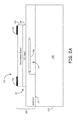
- FIGS. 2A-2C are diagrams that illustrate a pressure sensor of one embodiment of the present invention.
- Figure 3 is a flow chart that illustrates a process of one embodiment of the present invention.
- Figures 4A and 4B are diagrams illustrating ion doping profiles of one embodiment of the present invention.
- Figures 5A and 5B are diagrams illustrating an SOI pressure sensor die of one embodiment of the present invention.
- Figure 5C is a diagram illustrating a pressure sensor of one embodiment of the present invention.
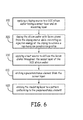
- Figure 6 is a flow chart that illustrates a process of one embodiment of the present invention.
- Figure 7 is a diagram illustrating one embodiment of the present invention.
- Embodiments of the present invention address two different error mechanisms that result in drift errors from operating Micro-electro-mechanical systems (MEMS) Silicon on Insulator (SOI) pressure sensors under high temperature/high pressure conditions.
- the first error mechanism involves ion migration that occurs in the SiO 2 material of the SiO 2 layer when the sensor's pressure sensing diagraph is flexed.
- the second error mechanism results from micro yielding within the SiO 2 layer when the sensor's pressure sensing diagraph is flexed.
- FIG. 1 illustrates one embodiment of a SOI pressure sensor die 100.
- SOI pressure sensor die 100 comprises a silicon substrate 112, an SOI layer 114 (that is, a layer of SiO 2 material) and a sensor layer 116 from which one or more piezoresistor elements will be formed, as described below.
- a cavity 110 formed within substrate 112 results in a thinned region of the substrate (shown generally at 111) located beneath the sensor layer 116 and SOI layer 114.
- This thinned region 111 functions to form a pressure sensing diagraph that deflects as a function of changes in pressure applied to it.
- SOI pressure sensor die 100 addresses ion migration within the SOI layer 114 by specifying an ion doping profile in sensor layer 116 that limits the penetration of ions introduced into SOI layer 114. This is explained in greater detail in the paragraphs below by reference to Figures 2A-2C .
- FIG. 2A illustrates one embodiment of a pressure sensor 200 comprising an SOI pressure sensor die 100 mounted onto a pedestal 225.
- the cavity 110 of SOI pressure sensor die 100 is oriented onto pedestal 225 such that its pressure sensing diaphragm 210 is in pressure communication with a backfilled volume 230 within pedestal 225.
- volume 230 provides a backfill pressure (using an inert gas, for example) against pressure sensing diaphragm 210 that determines the zero state for sensor 200.
- piezoresistor elements 210 are formed by doping boron atoms into sensor layer 116, resulting in a P++ epitaxial layer.
- piezoresistor elements 210 and traces for metalized interconnects 212 are etched away and metalized to leave piezoresistor elements 210 and traces for metalized interconnects 212.
- pressure sensing diaphragm 210 in response to a positive pressure 260 applied to SOI pressure sensor die 100, pressure sensing diaphragm 210 (including piezoresistor elements 210 and SOI layer 114) flexes inwards into volume 230 (as shown at 215). Because the resistance of piezoresistor elements 210 change as a function of this distortion, changes in this resistance are electrically sensed to provide a measurement of pressure 260.
- the sensitivity of a piezoresistor element is optimized by providing a high level of doping uniformly throughout the sensor layer 116 thickness.
- the levels of doping energy and temperature exposures needed to obtain this doping uniformity result in over driving boron atoms though the silicon/oxide interface and into the SOI layer 114.
- These atoms, which may be ionic in nature, in the SOI layer 114 are therefore available to redistribute themselves during applied pressure due to the diaphragm 210 surface tension strains or to produce trap sites at the interface which may be strain activated.
- ions 214 will migrate within SOI layer 114 away from areas of compression (such as shown at 232, for example) towards areas of tensions (such as shown at 234, for example).
- the ion movement rate is exponential with temperature. The result is that this effect is larger at higher temperatures.
- SOI pressure sensor die 100 avoids these errors due to ion migration by controlling the concentration of boron atoms injected into SOI layer 114 during doping of sensor layer 116.
- concentration of boron atoms injected into SOI layer 114 the number of ions is greatly reduced, minimizing the instability caused by ions moving due to strain fields as well as any trap sites at the interface or in the oxide.
- this is achieved by a doping and diffusing process that results in piezoresistor elements 210 having a doping profile characterized as a top-heavy ion penetration profile.
- the method begins at 310 with applying a doping source to a SOI silicon wafer having a sensor layer and an insulating layer.
- the process performed at block 310 comprises applying the doping source across the top surface 117 of SOI pressure die 100.
- the method proceeds to 320 with doping the silicon wafer with Boron atoms from the doping source while controlling an injection energy of the doping to achieve a top-heavy ion penetration profile.
- blocks 310 and 320 are performed within a standard doping furnace.
- a top-heavy ion penetration profile means that a peak in the concentration of Boron atoms occurs at a depth of less than 50% into the Silicon sensor layer as referenced from the surface where the doping source is applied.
- Figure 4A illustrates generally at 410 an example of doping profile characterizes as a top-heavy ion penetration profile. That means, for this doping profile, the peak in ion concentration (shown at 415) occurs at a depth of less than 50% penetration into sensor layer 116 from surface 117.
- the concentration of Boron atoms comprises a top-heavy ion penetration profile that peaks at a penetration between 33%-40%.
- the method next proceeds to 330 with applying a heat source to diffuse the Boron atoms throughout the sensor layer of the SOI silicon wafer.
- the diffusion step of at block 330 will function to flatten out the distribution of Boron atoms, the duration of diffusion may be controlled so that a top-heavy ion penetration profile is maintained after diffusion as shown in Figure 4B .
- This process will result in a gradient of resistance across the piezoresitor elements formed from the sensor layer, which may produce a device having less sensitivity than one with a uniform resistance distribution.
- the resulting sensor is significantly less susceptible to measurement drifts caused by ion migration in the SiO 2 of the SOI layer and to trap generation caused by the presence of boron.
- Figures 5A and 5B illustrates another embodiment of the present invention that addresses drift errors caused by micro yielding within the SiO 2 layer.
- Figures 5A and 5B shows an SOI sensor die 510 comprising a substrate 512, an SOI layer 514 of SiO 2 and a silicon sensor layer 516 (such as die 100 describe above).
- Figure 5C illustrates one embodiment of a pressure sensor 550 comprising an SOI pressure sensor die 510 mounted onto a pedestal 525.
- the cavity 515 of SOI pressure sensor die 510 is oriented onto pedestal 525 such that its pressure sensing diaphragm 526 is in pressure communication with a backfilled volume 530 within pedestal5225.
- volume 530 provides a backfill pressure (using an inert gas, for example) against pressure sensing diaphragm 526 that determines the zero state for sensor 550.
- pressure sensing diaphragm 526 in response to a positive pressure 560 applied to SOI pressure sensor die 510, pressure sensing diaphragm 526 (including piezoresistor elements 520 and SOI layer 514) flexes inwards into volume 530 (as shown at 515). Because the resistance of piezoresistor elements 520 change as a function of this distortion, changes in this resistance are electrically sensed to provide a measurement of pressure 560.
- piezoresistor elements 520 parts of sensor layer 516 are etched away leaving piezoresistor element 520 and traces for metalized interconnects 522.
- the surface of the die is largely the exposed SiO 2 of the SOI layer 514.
- the SiO 2 of the exposed SOI layer 514 behaves as a brittle material with little hysteresis or yielding.
- the SiO 2 of the SOI layer 514 takes on the characteristics of a more ductile material.
- the micro yielding is gradually reversed until the original mechanical zero is reached.
- this reversal process can take weeks to complete.
- the ongoing change in shape of die 510's diaphragm 526 is sensed by piezoresistor elements 520 as a change in measured pressure that does not correspond to any actual change in pressure.
- the reversal process itself introduces a dynamically changing drift error.
- Figure 5B illustrates the further etching performed to address this source of measurement drift error.
- die 500 is etched again, this time to remove portions of SiO 2 from the SOI layer.
- the Si0 2 material is removed except for those portions not supporting piezoresistor element 520 and traces for metalized interconnects 522. This removes the SOI layer from the high tensile stress areas of the die so that non-repeatability due to micro yielding is eliminated.
- the SOI layer can be etched to a pattern conforming to the piezoresitance elements. That is, portions of the SOI layer not directly support the piezoresitance element are removed to that the pattern of remaining SOI layer 514 material matches the pattern of remaining sensor level 516 material.
- any of the techniques described above for addressing measurement drift errors cause by deformation of SOI layer at high temperatures and pressures can used either individually within embodiments of the present invention or combined and used in conjunction in still other embodiments.
- the sensor layer 516 of SOI sensor die 500 is fabricated with a top-heavy ion penetration profile such as described with respect to SOI sensor die 100.
- the descriptions of various embodiments and their alternatives described herein may be used in various combinations with each other.
- Figure 6 illustrates one embodiment where blocks 310, 320 and 330 of the method of Figure 3 are followed by etching one or more piezoresistance elements from the sensor layer at block 610 and etching the insulating layer to a pattern conforming to the piezoresistance elements at block 620.
- Figure 7 illustrates yet another embodiment of a SOI pressure sensor device 730 comprising a SOI sensor die 710 with one or more piezoresistance elements 711 coupled by leads 715 and 716 to a Wheatstone bridge circuit 720.
- Wheatstone bridge circuit 720 provides an electric voltage across piezoresistance elements 711 and outputs a measurement signal 722 that varies as a function of pressure sensed by SOI sensor die 710.
- SOI sensor die 710 comprises a die such as SOI sensor die 100 (having a top-heavy ion penetration profile), SOI sensor die 510 (having an SOI layer etched to conform with a pattern of the sensor layer), or a combination of both features. Accordingly, the descriptions an alternatives discussed above for those embodiments apply to SOI pressure sensor device 730 as well.
- Example 1 includes a Silicon-on-insulator (SOI) pressure sensor die, the die comprising a substrate comprising Si material, the substrate having a first surface and an opposing second surface; an SOI layer comprising SiO 2 material deposited on the first surface; a sensor layer comprising doped Si material deposited on the SOI layer, the SOI layer separating the sensor layer from the substrate; wherein the doped Si material possesses an ion doping profile conforming to a top-heavy ion penetration profile.
- SOI Silicon-on-insulator
- Example 2 includes the die of Example 1 wherein the doped Si material is doped with Boron atoms.
- Example 3 includes the die of Example 1 or 2, wherein the doped Si material is doped with Boron atom such that a peak concentration of Boron atoms occurs between 33-40% penetration from a top surface of the sensor layer.
- Example 4 includes the die of Examples 1, 2 or 3 wherein the doped Si material forms a P++ doped epitaxial layer.
- Example 5 includes the die of Examples 1, 2, 3, or 4 wherein the doped sensor layer comprises one or more piezoresistance elements formed from the doped Si material.
- Example 6 includes the die of Examples 1, 2, 3, 4 or 5 further including a Wheatstone bridge circuit formed on the substrate and electrically coupled to the one or more piezoresistance elements.
- Example 7 includes the die of Examples 5 or 6 wherein the SOI layer is patterned to conform to a pattern of the one or more piezoresistance elements formed from the doped Si material.
- Example 8 includes the die of Example 7, further including a Wheatstone bridge circuit coupled to the one or more piezoresistance elements.
- Example 9 includes the die of any of Examples 1-8 wherein the second surface of the substrate is mounted to a pedestal having a sealed volume having a backfill pressure; the substrate further comprising a cavity formed in the second surface of the substrate, wherein the one or more piezoresistance elements are aligned with the cavity to define a pressure sensing diaphragm and the pressure sensing diaphragm is in pressure communication with the sealed volume.
- Example 10 includes a Silicon-on-insulator (SOI) pressure sensor die, the die comprising a substrate comprising Si material, the substrate having a first surface and an opposing second surface; an SOI layer comprising SiO 2 material deposited on the first surface; a sensor layer comprising doped Si material deposited on the SOI layer, the SOI layer separating the sensor layer from the substrate; wherein the SOI layer is etched into a pattern conforming to a pattern of the sensor layer.
- SOI Silicon-on-insulator
- Example 11 includes the die of Example 10 wherein the second surface of the substrate is mounted to a pedestal having a sealed volume having a backfill pressure, the substrate further comprising a cavity formed in the second surface of the substrate, wherein one or more piezoresistance elements are aligned with the cavity to define a pressure sensing diaphragm and the pressure sensing diaphragm is in pressure communication with the sealed volume.
- Example 12 includes the die of any of Examples 10-11 wherein the doped Si material is doped with Boron atoms and comprises a doping profile conforming to a top-heavy ion penetration profile.
- Example 13 includes the die of Example 12 wherein the doped Si material is doped with Boron atoms such that a peak concentration of Boron atoms occurs between 33-40% penetration from a top surface of the sensor layer.
- Example 14 includes the die of any of Examples 10-13 wherein the doped Si material forms a P++ doped epitaxial layer.
- Example 15 includes the die of any of Examples 10-14 wherein the sensor layer comprises one or more piezoresistance elements formed from the doped Si material.
- Example 16 includes the die of any of Examples 11 and 15 further comprising a Wheatstone bridge circuit formed on the substrate and electrically coupled to the one or more piezoresistance elements
- Example 17 includes a method for applying a doping source to a silicon-on-insulator (SOI) silicon wafer having a sensor layer and an insulating layer comprising SiO 2 material; doping the silicon wafer with Boron atoms from the doping source while controlling an injection energy of the doping to achieve a top-heavy ion penetration profile; and applying a heat source to diffuse the Boron atoms throughout the sensor layer of the SOI silicon wafer.
- SOI silicon-on-insulator
- Example 18 includes the method of Example 17 further including etching one or more piezoresistance elements from the sensor layer.
- Example 19 includes the method of Example 18 further including etching a Wheatstone bridge circuit from the sensor layer, the Wheatstone bridge circuit coupled to the one or more piezoresistance elements.
- Example 20 includes the method of Examples 18 or 19 further including etching the insulating layer to a pattern conforming to the one or more piezoresistance elements.
Landscapes
- Physics & Mathematics (AREA)
- General Physics & Mathematics (AREA)
- Thermal Sciences (AREA)
- Engineering & Computer Science (AREA)
- Computer Hardware Design (AREA)
- Microelectronics & Electronic Packaging (AREA)
- Chemical & Material Sciences (AREA)
- Analytical Chemistry (AREA)
- Measuring Fluid Pressure (AREA)
- Pressure Sensors (AREA)
Applications Claiming Priority (1)
| Application Number | Priority Date | Filing Date | Title |
|---|---|---|---|
| US13/412,264 US8813580B2 (en) | 2012-03-05 | 2012-03-05 | Apparatus and processes for silicon on insulator MEMS pressure sensors |
Publications (3)
| Publication Number | Publication Date |
|---|---|
| EP2637008A2 true EP2637008A2 (de) | 2013-09-11 |
| EP2637008A3 EP2637008A3 (de) | 2015-07-01 |
| EP2637008B1 EP2637008B1 (de) | 2017-03-22 |
Family
ID=47845731
Family Applications (1)
| Application Number | Title | Priority Date | Filing Date |
|---|---|---|---|
| EP13156859.4A Active EP2637008B1 (de) | 2012-03-05 | 2013-02-26 | Vorrichtung und Verfahren für Silicium auf Isolator-MEMS-Drucksensoren |
Country Status (3)
| Country | Link |
|---|---|
| US (1) | US8813580B2 (de) |
| EP (1) | EP2637008B1 (de) |
| CA (1) | CA2807671A1 (de) |
Cited By (3)
| Publication number | Priority date | Publication date | Assignee | Title |
|---|---|---|---|---|
| CN109545953A (zh) * | 2018-12-24 | 2019-03-29 | 中国航空工业集团公司西安飞行自动控制研究所 | 一种高温压力传感器芯片的制备方法 |
| GB2568578A (en) * | 2017-09-14 | 2019-05-22 | Sensata Technologies Inc | Pressure sensor with improved strain gauge |
| WO2021170314A1 (de) * | 2020-02-27 | 2021-09-02 | Tdk Electronics Ag | Sensor und verfahren zur herstellung eines sensors |
Families Citing this family (6)
| Publication number | Priority date | Publication date | Assignee | Title |
|---|---|---|---|---|
| US9581511B2 (en) | 2013-10-15 | 2017-02-28 | Meggitt (Orange County), Inc. | Microelectromechanical pressure sensors |
| CN106124117B (zh) * | 2016-06-14 | 2019-04-23 | 中国科学院地质与地球物理研究所 | 一种双空腔压力计芯片及其制造工艺 |
| US10809139B2 (en) * | 2018-02-14 | 2020-10-20 | Carefusion 303, Inc. | Integrated sensor to monitor fluid delivery |
| JP6865787B2 (ja) * | 2019-05-30 | 2021-04-28 | 三菱電機株式会社 | 半導体歪検出素子及びmemsアクチュエータデバイス |
| DE102020105214A1 (de) * | 2020-02-27 | 2021-09-02 | Endress+Hauser SE+Co. KG | Vibronischer Multisensor |
| CN115326249B (zh) * | 2021-06-25 | 2025-08-22 | 苏州跃芯微传感技术有限公司 | 一种mems压力传感器及其的制作方法 |
Family Cites Families (15)
| Publication number | Priority date | Publication date | Assignee | Title |
|---|---|---|---|---|
| DE69917943T2 (de) * | 1999-02-15 | 2005-06-23 | Yamatake Corp. | Halbleiter-drucksensor |
| US6566158B2 (en) * | 2001-08-17 | 2003-05-20 | Rosemount Aerospace Inc. | Method of preparing a semiconductor using ion implantation in a SiC layer |
| GB0200879D0 (en) * | 2002-01-16 | 2002-03-06 | Univ Surrey | Ion implanted junctions in silicon wafers |
| JP2004177343A (ja) * | 2002-11-28 | 2004-06-24 | Fujikura Ltd | 圧力センサ |
| US6718830B1 (en) * | 2003-05-20 | 2004-04-13 | Honeywell International, Inc. | Customized span compensation of SOI pressure sensor |
| US6952041B2 (en) * | 2003-07-25 | 2005-10-04 | Robert Bosch Gmbh | Anchors for microelectromechanical systems having an SOI substrate, and method of fabricating same |
| US7527997B2 (en) * | 2005-04-08 | 2009-05-05 | The Research Foundation Of State University Of New York | MEMS structure with anodically bonded silicon-on-insulator substrate |
| US7538401B2 (en) * | 2005-05-03 | 2009-05-26 | Rosemount Aerospace Inc. | Transducer for use in harsh environments |
| US7231828B2 (en) | 2005-09-23 | 2007-06-19 | Kulite Semiconductor Products, Inc. | High temperature pressure sensing system |
| US7258018B2 (en) * | 2005-10-26 | 2007-08-21 | Kulite Semiconductor Products, Inc. | High accuracy, high temperature, redundant media protected differential transducers |
| US7475597B2 (en) * | 2006-02-27 | 2009-01-13 | Auxitrol S.A. | Stress isolated pressure sensing die |
| US7615834B2 (en) * | 2006-02-28 | 2009-11-10 | The Board Of Trustees Of The Leland Stanford Junior University | Capacitive micromachined ultrasonic transducer(CMUT) with varying thickness membrane |
| US20090120194A1 (en) * | 2007-11-08 | 2009-05-14 | Honeywell International Inc. | Silicon pressure sensor |
| US7775119B1 (en) * | 2009-03-03 | 2010-08-17 | S3C, Inc. | Media-compatible electrically isolated pressure sensor for high temperature applications |
| JP2011031385A (ja) * | 2009-07-07 | 2011-02-17 | Rohm Co Ltd | Memsセンサ |
-
2012
- 2012-03-05 US US13/412,264 patent/US8813580B2/en active Active
-
2013
- 2013-02-26 CA CA2807671A patent/CA2807671A1/en not_active Abandoned
- 2013-02-26 EP EP13156859.4A patent/EP2637008B1/de active Active
Non-Patent Citations (1)
| Title |
|---|
| None |
Cited By (8)
| Publication number | Priority date | Publication date | Assignee | Title |
|---|---|---|---|---|
| GB2568578A (en) * | 2017-09-14 | 2019-05-22 | Sensata Technologies Inc | Pressure sensor with improved strain gauge |
| US10557770B2 (en) | 2017-09-14 | 2020-02-11 | Sensata Technologies, Inc. | Pressure sensor with improved strain gauge |
| GB2568578B (en) * | 2017-09-14 | 2020-10-07 | Sensata Technologies Inc | Pressure sensor with improved strain gauge |
| CN109545953A (zh) * | 2018-12-24 | 2019-03-29 | 中国航空工业集团公司西安飞行自动控制研究所 | 一种高温压力传感器芯片的制备方法 |
| CN109545953B (zh) * | 2018-12-24 | 2023-01-17 | 中国航空工业集团公司西安飞行自动控制研究所 | 一种高温压力传感器芯片的制备方法 |
| WO2021170314A1 (de) * | 2020-02-27 | 2021-09-02 | Tdk Electronics Ag | Sensor und verfahren zur herstellung eines sensors |
| CN114286929A (zh) * | 2020-02-27 | 2022-04-05 | Tdk电子股份有限公司 | 传感器和制造传感器的方法 |
| CN114286929B (zh) * | 2020-02-27 | 2024-06-18 | Tdk电子股份有限公司 | 传感器和制造传感器的方法 |
Also Published As
| Publication number | Publication date |
|---|---|
| US20130228022A1 (en) | 2013-09-05 |
| CA2807671A1 (en) | 2013-09-05 |
| US8813580B2 (en) | 2014-08-26 |
| EP2637008A3 (de) | 2015-07-01 |
| EP2637008B1 (de) | 2017-03-22 |
Similar Documents
| Publication | Publication Date | Title |
|---|---|---|
| US8813580B2 (en) | Apparatus and processes for silicon on insulator MEMS pressure sensors | |
| US5199298A (en) | Wall shear stress sensor | |
| KR100265876B1 (ko) | 미세가공된고감도압력센서및음향트랜스듀서 | |
| US11054327B2 (en) | Microelectromechanical piezoresistive pressure sensor with self-test capability and corresponding manufacturing process | |
| KR910008380A (ko) | 자기교정 기능을 가진 검출장치 | |
| CN101266176A (zh) | 硅硅键合的绝缘体上硅的高温压力传感器芯片及制作方法 | |
| US9352955B2 (en) | MEMS pressure sensor with improved insensitivity to thermo-mechanical stress | |
| CN111811726B (zh) | 用于电容式传感器或开关设备的微机械构件 | |
| JP4929753B2 (ja) | 薄膜構造体の形成方法並びに薄膜構造体、振動センサ、圧力センサ及び加速度センサ | |
| JPS62232171A (ja) | 半導体加速度センサ | |
| KR101652369B1 (ko) | 습식 및 건식 식각공정을 이용한 압저항형 압력센서 제조방법 | |
| CN109545953A (zh) | 一种高温压力传感器芯片的制备方法 | |
| CN103991836A (zh) | 微机电系统传感器及其制造方法 | |
| Su et al. | Fabrication of a piezoresistive barometric pressure sensor by a silicon‐on‐nothing technology | |
| JP3536817B2 (ja) | 半導体力学量センサ及びその製造方法 | |
| RU2457577C1 (ru) | Многофункциональный измерительный модуль | |
| JPH08107219A (ja) | 半導体加速度センサ及び半導体加速度センサの製造方法 | |
| CN1142438C (zh) | 深沟侧壁扩散和电绝缘薄膜填充制造压阻加速度传感器及其制造方法 | |
| CN203200012U (zh) | 微机电系统传感器 | |
| JP2696894B2 (ja) | 半導体圧力センサ | |
| JPS6260270A (ja) | 圧力センサのダイアフラム形成法 | |
| Keulemans et al. | Nonlinearity compensation for MEMS pressure sensors with piezoresistors at the neutral position | |
| Yu et al. | A piezoresistive pressure sensor with improved sensitivity in low pressure condition | |
| JP2002350259A (ja) | 半導体圧力センサおよびその製造方法 | |
| Je et al. | Surface Micromachined Pressure Sensor with Internal Substrate Vacuum Cavity |
Legal Events
| Date | Code | Title | Description |
|---|---|---|---|
| PUAI | Public reference made under article 153(3) epc to a published international application that has entered the european phase |
Free format text: ORIGINAL CODE: 0009012 |
|
| 17P | Request for examination filed |
Effective date: 20130226 |
|
| AK | Designated contracting states |
Kind code of ref document: A2 Designated state(s): AL AT BE BG CH CY CZ DE DK EE ES FI FR GB GR HR HU IE IS IT LI LT LU LV MC MK MT NL NO PL PT RO RS SE SI SK SM TR |
|
| AX | Request for extension of the european patent |
Extension state: BA ME |
|
| PUAL | Search report despatched |
Free format text: ORIGINAL CODE: 0009013 |
|
| AK | Designated contracting states |
Kind code of ref document: A3 Designated state(s): AL AT BE BG CH CY CZ DE DK EE ES FI FR GB GR HR HU IE IS IT LI LT LU LV MC MK MT NL NO PL PT RO RS SE SI SK SM TR |
|
| AX | Request for extension of the european patent |
Extension state: BA ME |
|
| RIC1 | Information provided on ipc code assigned before grant |
Ipc: G01L 9/06 20060101ALI20150522BHEP Ipc: G01L 9/00 20060101AFI20150522BHEP |
|
| 17Q | First examination report despatched |
Effective date: 20150626 |
|
| RAP1 | Party data changed (applicant data changed or rights of an application transferred) |
Owner name: HONEYWELL INTERNATIONAL INC. |
|
| GRAP | Despatch of communication of intention to grant a patent |
Free format text: ORIGINAL CODE: EPIDOSNIGR1 |
|
| INTG | Intention to grant announced |
Effective date: 20161012 |
|
| GRAS | Grant fee paid |
Free format text: ORIGINAL CODE: EPIDOSNIGR3 |
|
| GRAA | (expected) grant |
Free format text: ORIGINAL CODE: 0009210 |
|
| AK | Designated contracting states |
Kind code of ref document: B1 Designated state(s): AL AT BE BG CH CY CZ DE DK EE ES FI FR GB GR HR HU IE IS IT LI LT LU LV MC MK MT NL NO PL PT RO RS SE SI SK SM TR |
|
| REG | Reference to a national code |
Ref country code: GB Ref legal event code: FG4D |
|
| REG | Reference to a national code |
Ref country code: CH Ref legal event code: EP |
|
| REG | Reference to a national code |
Ref country code: AT Ref legal event code: REF Ref document number: 878269 Country of ref document: AT Kind code of ref document: T Effective date: 20170415 |
|
| REG | Reference to a national code |
Ref country code: IE Ref legal event code: FG4D |
|
| REG | Reference to a national code |
Ref country code: DE Ref legal event code: R096 Ref document number: 602013018780 Country of ref document: DE |
|
| REG | Reference to a national code |
Ref country code: NL Ref legal event code: MP Effective date: 20170322 |
|
| PG25 | Lapsed in a contracting state [announced via postgrant information from national office to epo] |
Ref country code: FI Free format text: LAPSE BECAUSE OF FAILURE TO SUBMIT A TRANSLATION OF THE DESCRIPTION OR TO PAY THE FEE WITHIN THE PRESCRIBED TIME-LIMIT Effective date: 20170322 Ref country code: GR Free format text: LAPSE BECAUSE OF FAILURE TO SUBMIT A TRANSLATION OF THE DESCRIPTION OR TO PAY THE FEE WITHIN THE PRESCRIBED TIME-LIMIT Effective date: 20170623 Ref country code: HR Free format text: LAPSE BECAUSE OF FAILURE TO SUBMIT A TRANSLATION OF THE DESCRIPTION OR TO PAY THE FEE WITHIN THE PRESCRIBED TIME-LIMIT Effective date: 20170322 Ref country code: LT Free format text: LAPSE BECAUSE OF FAILURE TO SUBMIT A TRANSLATION OF THE DESCRIPTION OR TO PAY THE FEE WITHIN THE PRESCRIBED TIME-LIMIT Effective date: 20170322 Ref country code: NO Free format text: LAPSE BECAUSE OF FAILURE TO SUBMIT A TRANSLATION OF THE DESCRIPTION OR TO PAY THE FEE WITHIN THE PRESCRIBED TIME-LIMIT Effective date: 20170622 |
|
| REG | Reference to a national code |
Ref country code: LT Ref legal event code: MG4D |
|
| REG | Reference to a national code |
Ref country code: AT Ref legal event code: MK05 Ref document number: 878269 Country of ref document: AT Kind code of ref document: T Effective date: 20170322 |
|
| PG25 | Lapsed in a contracting state [announced via postgrant information from national office to epo] |
Ref country code: LV Free format text: LAPSE BECAUSE OF FAILURE TO SUBMIT A TRANSLATION OF THE DESCRIPTION OR TO PAY THE FEE WITHIN THE PRESCRIBED TIME-LIMIT Effective date: 20170322 Ref country code: RS Free format text: LAPSE BECAUSE OF FAILURE TO SUBMIT A TRANSLATION OF THE DESCRIPTION OR TO PAY THE FEE WITHIN THE PRESCRIBED TIME-LIMIT Effective date: 20170322 Ref country code: BG Free format text: LAPSE BECAUSE OF FAILURE TO SUBMIT A TRANSLATION OF THE DESCRIPTION OR TO PAY THE FEE WITHIN THE PRESCRIBED TIME-LIMIT Effective date: 20170622 Ref country code: SE Free format text: LAPSE BECAUSE OF FAILURE TO SUBMIT A TRANSLATION OF THE DESCRIPTION OR TO PAY THE FEE WITHIN THE PRESCRIBED TIME-LIMIT Effective date: 20170322 |
|
| PG25 | Lapsed in a contracting state [announced via postgrant information from national office to epo] |
Ref country code: NL Free format text: LAPSE BECAUSE OF FAILURE TO SUBMIT A TRANSLATION OF THE DESCRIPTION OR TO PAY THE FEE WITHIN THE PRESCRIBED TIME-LIMIT Effective date: 20170322 |
|
| PG25 | Lapsed in a contracting state [announced via postgrant information from national office to epo] |
Ref country code: CZ Free format text: LAPSE BECAUSE OF FAILURE TO SUBMIT A TRANSLATION OF THE DESCRIPTION OR TO PAY THE FEE WITHIN THE PRESCRIBED TIME-LIMIT Effective date: 20170322 Ref country code: ES Free format text: LAPSE BECAUSE OF FAILURE TO SUBMIT A TRANSLATION OF THE DESCRIPTION OR TO PAY THE FEE WITHIN THE PRESCRIBED TIME-LIMIT Effective date: 20170322 Ref country code: SK Free format text: LAPSE BECAUSE OF FAILURE TO SUBMIT A TRANSLATION OF THE DESCRIPTION OR TO PAY THE FEE WITHIN THE PRESCRIBED TIME-LIMIT Effective date: 20170322 Ref country code: EE Free format text: LAPSE BECAUSE OF FAILURE TO SUBMIT A TRANSLATION OF THE DESCRIPTION OR TO PAY THE FEE WITHIN THE PRESCRIBED TIME-LIMIT Effective date: 20170322 Ref country code: AT Free format text: LAPSE BECAUSE OF FAILURE TO SUBMIT A TRANSLATION OF THE DESCRIPTION OR TO PAY THE FEE WITHIN THE PRESCRIBED TIME-LIMIT Effective date: 20170322 Ref country code: RO Free format text: LAPSE BECAUSE OF FAILURE TO SUBMIT A TRANSLATION OF THE DESCRIPTION OR TO PAY THE FEE WITHIN THE PRESCRIBED TIME-LIMIT Effective date: 20170322 |
|
| PG25 | Lapsed in a contracting state [announced via postgrant information from national office to epo] |
Ref country code: SM Free format text: LAPSE BECAUSE OF FAILURE TO SUBMIT A TRANSLATION OF THE DESCRIPTION OR TO PAY THE FEE WITHIN THE PRESCRIBED TIME-LIMIT Effective date: 20170322 Ref country code: IS Free format text: LAPSE BECAUSE OF FAILURE TO SUBMIT A TRANSLATION OF THE DESCRIPTION OR TO PAY THE FEE WITHIN THE PRESCRIBED TIME-LIMIT Effective date: 20170722 Ref country code: PL Free format text: LAPSE BECAUSE OF FAILURE TO SUBMIT A TRANSLATION OF THE DESCRIPTION OR TO PAY THE FEE WITHIN THE PRESCRIBED TIME-LIMIT Effective date: 20170322 Ref country code: PT Free format text: LAPSE BECAUSE OF FAILURE TO SUBMIT A TRANSLATION OF THE DESCRIPTION OR TO PAY THE FEE WITHIN THE PRESCRIBED TIME-LIMIT Effective date: 20170724 |
|
| REG | Reference to a national code |
Ref country code: DE Ref legal event code: R097 Ref document number: 602013018780 Country of ref document: DE |
|
| PLBE | No opposition filed within time limit |
Free format text: ORIGINAL CODE: 0009261 |
|
| STAA | Information on the status of an ep patent application or granted ep patent |
Free format text: STATUS: NO OPPOSITION FILED WITHIN TIME LIMIT |
|
| PG25 | Lapsed in a contracting state [announced via postgrant information from national office to epo] |
Ref country code: DK Free format text: LAPSE BECAUSE OF FAILURE TO SUBMIT A TRANSLATION OF THE DESCRIPTION OR TO PAY THE FEE WITHIN THE PRESCRIBED TIME-LIMIT Effective date: 20170322 |
|
| REG | Reference to a national code |
Ref country code: FR Ref legal event code: PLFP Year of fee payment: 6 |
|
| 26N | No opposition filed |
Effective date: 20180102 |
|
| PG25 | Lapsed in a contracting state [announced via postgrant information from national office to epo] |
Ref country code: IT Free format text: LAPSE BECAUSE OF FAILURE TO SUBMIT A TRANSLATION OF THE DESCRIPTION OR TO PAY THE FEE WITHIN THE PRESCRIBED TIME-LIMIT Effective date: 20170322 Ref country code: SI Free format text: LAPSE BECAUSE OF FAILURE TO SUBMIT A TRANSLATION OF THE DESCRIPTION OR TO PAY THE FEE WITHIN THE PRESCRIBED TIME-LIMIT Effective date: 20170322 |
|
| REG | Reference to a national code |
Ref country code: DE Ref legal event code: R119 Ref document number: 602013018780 Country of ref document: DE |
|
| REG | Reference to a national code |
Ref country code: CH Ref legal event code: PL |
|
| PG25 | Lapsed in a contracting state [announced via postgrant information from national office to epo] |
Ref country code: MC Free format text: LAPSE BECAUSE OF FAILURE TO SUBMIT A TRANSLATION OF THE DESCRIPTION OR TO PAY THE FEE WITHIN THE PRESCRIBED TIME-LIMIT Effective date: 20170322 |
|
| REG | Reference to a national code |
Ref country code: IE Ref legal event code: MM4A |
|
| REG | Reference to a national code |
Ref country code: BE Ref legal event code: MM Effective date: 20180228 |
|
| PG25 | Lapsed in a contracting state [announced via postgrant information from national office to epo] |
Ref country code: CH Free format text: LAPSE BECAUSE OF NON-PAYMENT OF DUE FEES Effective date: 20180228 Ref country code: LU Free format text: LAPSE BECAUSE OF NON-PAYMENT OF DUE FEES Effective date: 20180226 Ref country code: LI Free format text: LAPSE BECAUSE OF NON-PAYMENT OF DUE FEES Effective date: 20180228 |
|
| PG25 | Lapsed in a contracting state [announced via postgrant information from national office to epo] |
Ref country code: IE Free format text: LAPSE BECAUSE OF NON-PAYMENT OF DUE FEES Effective date: 20180226 Ref country code: DE Free format text: LAPSE BECAUSE OF NON-PAYMENT OF DUE FEES Effective date: 20180901 |
|
| PG25 | Lapsed in a contracting state [announced via postgrant information from national office to epo] |
Ref country code: BE Free format text: LAPSE BECAUSE OF NON-PAYMENT OF DUE FEES Effective date: 20180228 |
|
| PG25 | Lapsed in a contracting state [announced via postgrant information from national office to epo] |
Ref country code: MT Free format text: LAPSE BECAUSE OF NON-PAYMENT OF DUE FEES Effective date: 20180226 |
|
| PG25 | Lapsed in a contracting state [announced via postgrant information from national office to epo] |
Ref country code: TR Free format text: LAPSE BECAUSE OF FAILURE TO SUBMIT A TRANSLATION OF THE DESCRIPTION OR TO PAY THE FEE WITHIN THE PRESCRIBED TIME-LIMIT Effective date: 20170322 |
|
| PG25 | Lapsed in a contracting state [announced via postgrant information from national office to epo] |
Ref country code: HU Free format text: LAPSE BECAUSE OF FAILURE TO SUBMIT A TRANSLATION OF THE DESCRIPTION OR TO PAY THE FEE WITHIN THE PRESCRIBED TIME-LIMIT; INVALID AB INITIO Effective date: 20130226 |
|
| PG25 | Lapsed in a contracting state [announced via postgrant information from national office to epo] |
Ref country code: CY Free format text: LAPSE BECAUSE OF FAILURE TO SUBMIT A TRANSLATION OF THE DESCRIPTION OR TO PAY THE FEE WITHIN THE PRESCRIBED TIME-LIMIT Effective date: 20170322 Ref country code: MK Free format text: LAPSE BECAUSE OF NON-PAYMENT OF DUE FEES Effective date: 20170322 |
|
| PG25 | Lapsed in a contracting state [announced via postgrant information from national office to epo] |
Ref country code: AL Free format text: LAPSE BECAUSE OF FAILURE TO SUBMIT A TRANSLATION OF THE DESCRIPTION OR TO PAY THE FEE WITHIN THE PRESCRIBED TIME-LIMIT Effective date: 20170322 |
|
| P01 | Opt-out of the competence of the unified patent court (upc) registered |
Effective date: 20230525 |
|
| PGFP | Annual fee paid to national office [announced via postgrant information from national office to epo] |
Ref country code: GB Payment date: 20260223 Year of fee payment: 14 |
|
| PGFP | Annual fee paid to national office [announced via postgrant information from national office to epo] |
Ref country code: FR Payment date: 20260224 Year of fee payment: 14 |