EP2634827A1 - Laminated piezoelectric element, injection device using same, and fuel injection system - Google Patents
Laminated piezoelectric element, injection device using same, and fuel injection system Download PDFInfo
- Publication number
- EP2634827A1 EP2634827A1 EP11836460.3A EP11836460A EP2634827A1 EP 2634827 A1 EP2634827 A1 EP 2634827A1 EP 11836460 A EP11836460 A EP 11836460A EP 2634827 A1 EP2634827 A1 EP 2634827A1
- Authority
- EP
- European Patent Office
- Prior art keywords
- external electrode
- piezoelectric element
- resin
- layer
- stacked body
- Prior art date
- Legal status (The legal status is an assumption and is not a legal conclusion. Google has not performed a legal analysis and makes no representation as to the accuracy of the status listed.)
- Granted
Links
- 238000002347 injection Methods 0.000 title claims abstract description 52
- 239000007924 injection Substances 0.000 title claims abstract description 52
- 239000000446 fuel Substances 0.000 title claims abstract description 37
- 229920005989 resin Polymers 0.000 claims abstract description 70
- 239000011347 resin Substances 0.000 claims abstract description 70
- 239000004020 conductor Substances 0.000 claims abstract description 60
- 239000004593 Epoxy Substances 0.000 claims description 12
- 239000012530 fluid Substances 0.000 claims description 6
- 238000000926 separation method Methods 0.000 abstract description 14
- 239000000243 solution Substances 0.000 abstract description 3
- 239000000919 ceramic Substances 0.000 description 16
- 238000006073 displacement reaction Methods 0.000 description 14
- 230000020169 heat generation Effects 0.000 description 10
- 230000001965 increasing effect Effects 0.000 description 9
- 239000000463 material Substances 0.000 description 8
- 239000000843 powder Substances 0.000 description 8
- BQCADISMDOOEFD-UHFFFAOYSA-N Silver Chemical compound [Ag] BQCADISMDOOEFD-UHFFFAOYSA-N 0.000 description 7
- 239000011230 binding agent Substances 0.000 description 7
- 229910052709 silver Inorganic materials 0.000 description 7
- 239000004332 silver Substances 0.000 description 7
- 230000000694 effects Effects 0.000 description 6
- 238000010304 firing Methods 0.000 description 6
- 229910000679 solder Inorganic materials 0.000 description 6
- 238000009825 accumulation Methods 0.000 description 5
- 230000008602 contraction Effects 0.000 description 5
- 229910052451 lead zirconate titanate Inorganic materials 0.000 description 5
- HFGPZNIAWCZYJU-UHFFFAOYSA-N lead zirconate titanate Chemical compound [O-2].[O-2].[O-2].[O-2].[O-2].[Ti+4].[Zr+4].[Pb+2] HFGPZNIAWCZYJU-UHFFFAOYSA-N 0.000 description 5
- 239000004014 plasticizer Substances 0.000 description 5
- 238000012360 testing method Methods 0.000 description 5
- 238000010521 absorption reaction Methods 0.000 description 4
- DOIRQSBPFJWKBE-UHFFFAOYSA-N dibutyl phthalate Chemical compound CCCCOC(=O)C1=CC=CC=C1C(=O)OCCCC DOIRQSBPFJWKBE-UHFFFAOYSA-N 0.000 description 4
- 239000011521 glass Substances 0.000 description 4
- 230000006872 improvement Effects 0.000 description 4
- 238000000034 method Methods 0.000 description 4
- 238000007650 screen-printing Methods 0.000 description 4
- 239000002002 slurry Substances 0.000 description 4
- 229910001252 Pd alloy Inorganic materials 0.000 description 3
- 239000000853 adhesive Substances 0.000 description 3
- 230000001070 adhesive effect Effects 0.000 description 3
- 230000008859 change Effects 0.000 description 3
- 238000002485 combustion reaction Methods 0.000 description 3
- 238000005259 measurement Methods 0.000 description 3
- 229910052751 metal Inorganic materials 0.000 description 3
- 239000002184 metal Substances 0.000 description 3
- SWELZOZIOHGSPA-UHFFFAOYSA-N palladium silver Chemical compound [Pd].[Ag] SWELZOZIOHGSPA-UHFFFAOYSA-N 0.000 description 3
- 229920000642 polymer Polymers 0.000 description 3
- 229920001296 polysiloxane Polymers 0.000 description 3
- 239000010935 stainless steel Substances 0.000 description 3
- 229910001220 stainless steel Inorganic materials 0.000 description 3
- 229910000906 Bronze Inorganic materials 0.000 description 2
- RYGMFSIKBFXOCR-UHFFFAOYSA-N Copper Chemical compound [Cu] RYGMFSIKBFXOCR-UHFFFAOYSA-N 0.000 description 2
- MQIUGAXCHLFZKX-UHFFFAOYSA-N Di-n-octyl phthalate Natural products CCCCCCCCOC(=O)C1=CC=CC=C1C(=O)OCCCCCCCC MQIUGAXCHLFZKX-UHFFFAOYSA-N 0.000 description 2
- XEEYBQQBJWHFJM-UHFFFAOYSA-N Iron Chemical compound [Fe] XEEYBQQBJWHFJM-UHFFFAOYSA-N 0.000 description 2
- KDLHZDBZIXYQEI-UHFFFAOYSA-N Palladium Chemical compound [Pd] KDLHZDBZIXYQEI-UHFFFAOYSA-N 0.000 description 2
- OAICVXFJPJFONN-UHFFFAOYSA-N Phosphorus Chemical compound [P] OAICVXFJPJFONN-UHFFFAOYSA-N 0.000 description 2
- BJQHLKABXJIVAM-UHFFFAOYSA-N bis(2-ethylhexyl) phthalate Chemical compound CCCCC(CC)COC(=O)C1=CC=CC=C1C(=O)OCC(CC)CCCC BJQHLKABXJIVAM-UHFFFAOYSA-N 0.000 description 2
- 239000010974 bronze Substances 0.000 description 2
- 229910052802 copper Inorganic materials 0.000 description 2
- 239000010949 copper Substances 0.000 description 2
- KUNSUQLRTQLHQQ-UHFFFAOYSA-N copper tin Chemical compound [Cu].[Sn] KUNSUQLRTQLHQQ-UHFFFAOYSA-N 0.000 description 2
- 238000005336 cracking Methods 0.000 description 2
- 230000002950 deficient Effects 0.000 description 2
- 238000010586 diagram Methods 0.000 description 2
- 238000011156 evaluation Methods 0.000 description 2
- 238000004519 manufacturing process Methods 0.000 description 2
- BASFCYQUMIYNBI-UHFFFAOYSA-N platinum Chemical compound [Pt] BASFCYQUMIYNBI-UHFFFAOYSA-N 0.000 description 2
- 230000010287 polarization Effects 0.000 description 2
- 229910052573 porcelain Inorganic materials 0.000 description 2
- 238000003466 welding Methods 0.000 description 2
- WSMQKESQZFQMFW-UHFFFAOYSA-N 5-methyl-pyrazole-3-carboxylic acid Chemical compound CC1=CC(C(O)=O)=NN1 WSMQKESQZFQMFW-UHFFFAOYSA-N 0.000 description 1
- ZTQSAGDEMFDKMZ-UHFFFAOYSA-N Butyraldehyde Chemical compound CCCC=O ZTQSAGDEMFDKMZ-UHFFFAOYSA-N 0.000 description 1
- 229910003781 PbTiO3 Inorganic materials 0.000 description 1
- 239000004642 Polyimide Substances 0.000 description 1
- ATJFFYVFTNAWJD-UHFFFAOYSA-N Tin Chemical compound [Sn] ATJFFYVFTNAWJD-UHFFFAOYSA-N 0.000 description 1
- 241000276425 Xiphophorus maculatus Species 0.000 description 1
- 229910052782 aluminium Inorganic materials 0.000 description 1
- XAGFODPZIPBFFR-UHFFFAOYSA-N aluminium Chemical compound [Al] XAGFODPZIPBFFR-UHFFFAOYSA-N 0.000 description 1
- 150000001408 amides Chemical class 0.000 description 1
- 238000010344 co-firing Methods 0.000 description 1
- 239000011248 coating agent Substances 0.000 description 1
- 238000000576 coating method Methods 0.000 description 1
- 230000000052 comparative effect Effects 0.000 description 1
- 238000010276 construction Methods 0.000 description 1
- 238000007606 doctor blade method Methods 0.000 description 1
- 238000001035 drying Methods 0.000 description 1
- 230000005684 electric field Effects 0.000 description 1
- 230000002708 enhancing effect Effects 0.000 description 1
- 230000007613 environmental effect Effects 0.000 description 1
- 239000003822 epoxy resin Substances 0.000 description 1
- 239000011888 foil Substances 0.000 description 1
- 239000002828 fuel tank Substances 0.000 description 1
- 238000000227 grinding Methods 0.000 description 1
- 230000001771 impaired effect Effects 0.000 description 1
- 229910052742 iron Inorganic materials 0.000 description 1
- 239000007788 liquid Substances 0.000 description 1
- GQYHUHYESMUTHG-UHFFFAOYSA-N lithium niobate Chemical compound [Li+].[O-][Nb](=O)=O GQYHUHYESMUTHG-UHFFFAOYSA-N 0.000 description 1
- 230000014759 maintenance of location Effects 0.000 description 1
- 239000013528 metallic particle Substances 0.000 description 1
- 238000002156 mixing Methods 0.000 description 1
- 239000000203 mixture Substances 0.000 description 1
- 238000012986 modification Methods 0.000 description 1
- 230000004048 modification Effects 0.000 description 1
- 238000000465 moulding Methods 0.000 description 1
- 229910052763 palladium Inorganic materials 0.000 description 1
- 239000002245 particle Substances 0.000 description 1
- 229910052697 platinum Inorganic materials 0.000 description 1
- 229920000058 polyacrylate Polymers 0.000 description 1
- 229920000647 polyepoxide Polymers 0.000 description 1
- 229920001721 polyimide Polymers 0.000 description 1
- 238000007639 printing Methods 0.000 description 1
- 230000008569 process Effects 0.000 description 1
- 230000009257 reactivity Effects 0.000 description 1
- 230000009467 reduction Effects 0.000 description 1
- 238000005096 rolling process Methods 0.000 description 1
- 238000007569 slipcasting Methods 0.000 description 1
- 238000005476 soldering Methods 0.000 description 1
Images


Classifications
-
- F—MECHANICAL ENGINEERING; LIGHTING; HEATING; WEAPONS; BLASTING
- F02—COMBUSTION ENGINES; HOT-GAS OR COMBUSTION-PRODUCT ENGINE PLANTS
- F02M—SUPPLYING COMBUSTION ENGINES IN GENERAL WITH COMBUSTIBLE MIXTURES OR CONSTITUENTS THEREOF
- F02M51/00—Fuel-injection apparatus characterised by being operated electrically
- F02M51/06—Injectors peculiar thereto with means directly operating the valve needle
- F02M51/0603—Injectors peculiar thereto with means directly operating the valve needle using piezoelectric or magnetostrictive operating means
-
- H—ELECTRICITY
- H10—SEMICONDUCTOR DEVICES; ELECTRIC SOLID-STATE DEVICES NOT OTHERWISE PROVIDED FOR
- H10N—ELECTRIC SOLID-STATE DEVICES NOT OTHERWISE PROVIDED FOR
- H10N30/00—Piezoelectric or electrostrictive devices
- H10N30/01—Manufacture or treatment
- H10N30/06—Forming electrodes or interconnections, e.g. leads or terminals
- H10N30/063—Forming interconnections, e.g. connection electrodes of multilayered piezoelectric or electrostrictive parts
-
- H—ELECTRICITY
- H10—SEMICONDUCTOR DEVICES; ELECTRIC SOLID-STATE DEVICES NOT OTHERWISE PROVIDED FOR
- H10N—ELECTRIC SOLID-STATE DEVICES NOT OTHERWISE PROVIDED FOR
- H10N30/00—Piezoelectric or electrostrictive devices
- H10N30/50—Piezoelectric or electrostrictive devices having a stacked or multilayer structure
- H10N30/508—Piezoelectric or electrostrictive devices having a stacked or multilayer structure adapted for alleviating internal stress, e.g. cracking control layers
-
- H—ELECTRICITY
- H10—SEMICONDUCTOR DEVICES; ELECTRIC SOLID-STATE DEVICES NOT OTHERWISE PROVIDED FOR
- H10N—ELECTRIC SOLID-STATE DEVICES NOT OTHERWISE PROVIDED FOR
- H10N30/00—Piezoelectric or electrostrictive devices
- H10N30/80—Constructional details
- H10N30/87—Electrodes or interconnections, e.g. leads or terminals
- H10N30/872—Interconnections, e.g. connection electrodes of multilayer piezoelectric or electrostrictive devices
-
- H—ELECTRICITY
- H10—SEMICONDUCTOR DEVICES; ELECTRIC SOLID-STATE DEVICES NOT OTHERWISE PROVIDED FOR
- H10N—ELECTRIC SOLID-STATE DEVICES NOT OTHERWISE PROVIDED FOR
- H10N30/00—Piezoelectric or electrostrictive devices
- H10N30/80—Constructional details
- H10N30/87—Electrodes or interconnections, e.g. leads or terminals
- H10N30/875—Further connection or lead arrangements, e.g. flexible wiring boards, terminal pins
Definitions
- the present invention relates to a multi-layer piezoelectric element used for, for example, a driving element (piezoelectric actuator), a sensor element, and a circuit element, as well as to an injection device and a fuel injection system using the same.
- a driving element piezoelectric actuator
- sensor element a sensor element
- circuit element a circuit element
- a multi-layer piezoelectric element comprising: a stacked body including stacked piezoelectric bodies and internal electrodes; a conductor layer disposed coveringly on a side surface of the stacked body so as to be elongated in a stacking direction of the stacked body to electrically connect with ends of the internal electrodes extended to the side surface of the stacked body; and an external electrode disposed on the conductor layer so as to extend along the stacking direction (See Patent Literature 1).
- a lead is electrically connected to one end (feeding end) of the external electrode to electrically connect with an external circuit to receive current supply from an external power source.
- Patent Literature 1 Japanese Unexamined Patent Publication JP-A 2002-61551
- multi-layer piezoelectric elements have been required to have the capability of long-time continuous driving operation under high-voltage conditions, which has resulted in an increasing demand for long-time retention of displacement and improvement in durability.
- a large electric current passes instantaneously through a portion for allowing the entry of electric current from the lead located at one end of the external electrode, with a consequent rise in temperature. Therefore, the bonded region of the external electrode, which is bonded to the conductor layer in an area near a feeding end, is prone to damage or separation.
- the invention has been devised in view of the conventional problem as mentioned supra, and accordingly an object of the invention is to provide a multi-layer piezoelectric element which suppresses damage or separation of an external electrode and improves durability, as well as to provide an injection device and a fuel injection system using the multi-layer piezoelectric element.
- the invention provides a multi-layer piezoelectric element including: a stacked body including stacked piezoelectric bodies and internal electrodes; a conductor layer disposed coveringly on a side surface of the stacked body so as to be elongated in a stacking direction of the stacked body to electrically connect with ends of the internal electrodes, which are extended to the side surface of the stacked body; and an external electrode disposed on the conductor layer, one end in the stacking direction of the external electrode being a feeding end, a bonded region of the external electrode, which is bonded to the conductor layer in an area near the feeding end, being covered with a resin.
- the invention provides an injection device including: a container provided with an injection hole; and the multi-layer piezoelectric element of the invention, a fluid stored in the container being injected through the injection hole by driving the multi-layer piezoelectric element.
- the invention provides an injection system including: a common rail configured to store a high-pressure fuel; the injection device of the invention, configure to inject the high-pressure fuel stored in the common rail; a pressure pump configured to supply the high-pressure fuel to the common rail; and an injection control unit configured to send a drive signal to the injection device.
- one end in the stacking direction of the external electrode is a feeding end, and the bonded region of the external electrode, which is bonded to the conductor layer in the area near the feeding end, is covered with a resin having large thermal capacity. Accordingly, heat can be accumulated in (absorbed by) the resin at the bonded end portion of the external electrode that undergoes generation of a large amount of heat. This makes it possible to suppress rapid temperature rise in the external electrode, and thus prevent the external electrode from damage, with consequent improvement in durability. Moreover, even when an amount of heat generation is large, the external electrode can be protected from damage due to breakage of the resin, rather than the external electrode.
- the strength of adhesion between the external electrode and the conductor layer at the bonded end portion can be enhanced, it never occurs that the multi-layer piezoelectric element suffers from damage due to separation of the external electrode. This helps increase the longevity of the multi-layer piezoelectric element.
- Fig. 1 is a perspective view showing an embodiment of a multi-layer piezoelectric element according to the invention
- Fig. 2 is an enlarged sectional view showing a major part of the multi-layer piezoelectric element 1 shown in Fig. 1 .
- the multi-layer piezoelectric element 1 shown in Figs. 1 and 2 includes a stacked body 2 including stacked piezoelectric bodies 21 and internal electrodes 3a, 3b; conductor layers 5a and 5b each disposed coveringly on a side surface of the stacked body 2 so as to be elongated in a stacking direction of the stacked body to electrically connect with ends of the internal electrodes 3a, 3b extended to the side surface of the stacked body 2; and external electrodes 4a and 4b disposed on the conductor layers 5a and 5b, respectively.
- One end in the stacking direction of the external electrode 4a, 4b is a feeding end, and a bonded region of the external electrode 4a, 4b, which is bonded to the conductor layer in an area near the feeding end, is covered with a resin 13.
- the stacked body 2 is configured to include an active section 2a in which piezoelectric bodies 21 and internal electrodes 3a, 3b are alternately laminated, and inactive sections 2b arranged at both ends in the stacking direction of the active section 2a, each of the inactive sections being configured so that a plurality of piezoelectric bodies 21 are laminated.
- the stacked body 2 has the form of a column having a length of 0.5 to 10 mm, a width of 0.5 to 10 mm, and a height of 1 to 10 mm, for example.
- the end of the internal electrode 3a and the end of the internal electrode 3b are extended to the opposite side surfaces (opposed side surfaces), respectively, of the stacked body 2.
- the piezoelectric body 21 is made of ceramics having a piezoelectric property.
- ceramics for example, a perovskite-type oxide made of lead zirconate titanate (PZT: PbZrO 3 -PbTiO 3 ), lithium niobate (LiNbO 3 ), lithium tantalate (LiTaO 3 ) or the like can be used.
- the internal electrode 3a, 3b is formed by means of co-firing together with the ceramics constituting the piezoelectric body 21.
- a conductor composed predominantly of a silver-palladium alloy whose reactivity with piezoelectric porcelain is low, or a conductor containing copper, platinum, or the like can be used.
- the stacked body 2 may be configured to include a to-be-broken layer (not shown) which is preferentially broken rather than the internal electrode 3a, 3b during driving operation.
- a to-be-broken layer (not shown) which is preferentially broken rather than the internal electrode 3a, 3b during driving operation.
- the to-be-broken layer is designed as a layer which is lower in strength than the internal electrode 3a, 3b and is thus prone to cracking under stress and provides stress reduction capability.
- the to-be-broken layer is made of an insufficiently-sintered piezoelectric layer, a piezoelectric layer or metallic layer bearing many porosities, or a layer containing independently-distributed piezoelectric particles and metallic particles.
- the provision of such a to-be-broken layer makes it possible to prevent the internal electrode 3a, 3b and the piezoelectric body 21 from cracking, because the to-be-broken layer becomes cracked preferentially when tensile stress is exerted in the stacking direction of the stacked body 2 as the result of expansion of the stacked body 2.
- the conductor layer 5a, 5b on the side surface of the stacked body 2 is coveringly disposed the conductor layer 5a, 5b so as to be elongated in the stacking direction to electrically connect with the ends of the internal electrodes 3a, 3b extended to that side surface. More specifically, the conductor layer 5a is electrically connected to the end of the internal electrode 3a extended to its respective side surface of the stacked body 2, and the conductor layer 5b is electrically connected to the end of the internal electrode 3b extended to its respective side surface of the stacked body 2. Note that the conductor layer 5a is omitted in Fig. 2 .
- the conductor layer 5a, 5b is made of an electrically conducting material such as silver, and preferably contains a glass component additionally for the sake of enhancing its adhesion to the stacked body 2.
- the conductor layer 5a, 5b can be formed by application of a paste made of silver and glass with subsequent baking process.
- the thickness of the conductor layer 5a, 5b falls within the range of 10 to 500 ⁇ m.
- the external electrode 4a, 4b is bonded to the conductor layer 5a, 5b. More specifically, the external electrode 4a is bonded to the conductor layer 5a by an electrically conducting bonding material (not shown), and the external electrode 4b is bonded to the conductor layer 5b by an electrically conducting bonding material(not shown). Note that the external electrode 4a and the conductor layer 5a are omitted in Figs. 1 and 2 .
- solder preferably, lead-free solder in view of environmental friendliness
- electrically conducting resin is desirable from the standpoints of heat resistance, adaptability to expansion and contraction of the stacked body 2, high strength of adhesion to the resin 13 as will hereafter be described, and minimization of the possibility of separation of the resin 13.
- the thickness of each of the electrically conducting bonding materials falls within the range of 5 ⁇ m to 500 ⁇ m.
- the external electrode 4a, 4b is a platy electrode made of metal such as copper, iron, stainless steel, or phosphor bronze, and has a width of 0.5 to 10 mm and a thickness of 0.01 to 1.0 mm, for example.
- the external electrode 4a, 4b is connected, at its one end in the stacking direction (feeding end), to an external circuit. That one end (feeding end) is connected with a lead (for example, a lead pin 12) via the above-described electrically conducting bonding material (not shown) or by means of welding.
- the external electrode 4a, 4b is preferably made to have slits, or have a meshed configuration or corrugated configuration in the interest of adaptability to expansion and contraction of the stacked body 2.
- the thickness is preferably in a range of from 10 to 500 ⁇ m, and in particular from 50 to 200 ⁇ m.
- the external electrode 4a, 4b can be plated with tin or silver to improve the electrical conductivity and thermal conductivity.
- the bonded region of the external electrode 4a, 4b, which is bonded to the conductor layer 5a, 5b in the area near one end (feeding end), is covered with the resin 13.
- the connected portion of the external electrode 4a, 4b which is connected to the lead pin 12 and is positioned at one end is a portion for allowing the entry of electric current that is most susceptible to heat generation.
- the bonded end portion of the external electrode 4a, 4b which is bonded to the conductor layer 5a, 5b in the area near one end, undergoes a large amount of heat generation.
- stainless steel is preferable to phosphor bronze from the viewpoint of ensuring adequate strength in the external electrode 4a, 4b when it is made thinly.
- the external electrode 4a, 4b is made thin using stainless steel, it will be of higher resistance, which leads to an increase in the amount of heat generation (temperature rise).
- the resin 13 by placing the resin 13 so that it covers the bonded region (bonded end portion) of the external electrode 4a, 4b which is bonded to the conductor layer 5a, 5b in the area near one end (feeding end), the heat evolved at the bonded end portion which undergoes a large amount of heat generation can be accumulated in (absorbed by) the resin.
- This makes it possible to suppress rapid temperature rise in the external electrode 4a, 4b and thus prevent the external electrode 4a, 4b from damage, with consequent improvement in durability.
- the external electrode 4a, 4b can be protected from damage due to breakage of the resin 13, rather than the external electrode 4a, 4b.
- the strength of adhesion between the external electrode 4a, 4b and the conductor layer 5a, 5b at the bonded end portion can be enhanced, it never occurs that the multi-layer piezoelectric element suffers from damage due to separation of the external electrode 4a, 4b. This helps increase the longevity of the multi-layer piezoelectric element.
- placement of the resin 13 to cover the connected portion of the external electrode 4a, 4b which is connected to the lead pin 12 and is positioned at one end (feeding end) is effective at suppressing rapid temperature rise in the external electrode 4a, 4b.
- setting of the resin 13 to be larger in width than the external electrode 4a, 4b, as well as placement of the resin 13 to cover, in addition to the external electrode 4a, 4b, the conductor layer 5a, 5b, is effective at suppressing separation of the external electrode 4a, 4b.
- the thickness of the resin 13 is from 10 to 500 ⁇ m, and preferably from 50 to 200 ⁇ m. If the thickness is less than 10 ⁇ m, the heat-accumulation effect (heat-absorption effect) and the effect of adherability of the resin 13 will be impaired. If the thickness exceeds 500 ⁇ m, the resin 13 will be prone to separation due to the difference in thermal expansion between the resin 13 and the external electrode 4a, 4b.
- a bonded region of the external electrode 4a, 4b which is bonded to the conductor layer 5a, 5b in an area near another end opposite to the feeding end, is covered with a resin 14.
- the bonded region positioned near the opposite end which is prone to separation also becomes resistant to separation by virtue of improved heat-accumulation capability and adherability, wherefore the longevity can be increased even further.
- the bonded regions of the external electrode 4a, 4b bonded to the conductor layer 5a, 5b are covered with the resin 13 and the resin 14, respectively, whereas any regions other than the bonded regions of the external electrode 4a, 4b bonded to the conductor layer 5a, 5b are not covered with the resin 13 as well as the resin 14. This makes it possible to suppress damage or separation of the external electrode 4a, 4b resulting from heat generation while permitting freedom of expansion and contraction of the stacked body 2.
- the resin 13, 14 is disposed at the inactive section 2b which includes stacked piezoelectric bodies 21 but does not include the internal electrodes 3a, 3b (inactive section 2b of poor thermal conductivity).
- the resin is capable of producing better heat-accumulation effect (heat-absorption effect) in the inactive section 2b insensitive to an instantaneous temperature change, wherefore the longevity can be increased.
- the inactive section 2b does not undergo expansion and contraction, it follows that the resin 13, 14 and the stacked body 2 (piezoelectric bodies) adhere firmly to each other and are thus less prone to mutual separation, with consequent improvement in durability.
- the multi-layer piezoelectric element 1 can be so designed that the conductor layer 5a, 5b and the external electrode 4a, 4b are each extended from the active section 2a to the inactive section 2b, and the resin 13, 14 lies across the active section 2a and the inactive section 2b.
- the multi-layer piezoelectric element 1 in the case where the external electrode 4a, 4b is so disposed as to have a protrusion on its feeding-end side, the protrusion extending beyond an end face of the stacked body 2, it is preferable that part of the end face of the stacked body 2 and part of the protrusion of the external electrode 4a, 4b are bonded to each other by the resin 13, 14.
- the area of contact between the resin 13, 14 and the external electrode 4a, 4b can be increased, with a consequent increase in the amount of heat accumulation (the amount of heat absorption). This makes it possible to suppress rapid heat generation and thereby prevent the external electrode 4a, 4b from damage. Accordingly, the longevity can be increased.
- the multi-layer piezoelectric element 1 is configured to form the bonded end portion of the external electrode 4a, 4b with a hole 41, the hole 41 being filled with the resin 13.
- Fig. 5 is a plan view illustrating the external electrode 4b-bearing surface of the construction as a top surface, assuming that the resin 13 is transparent. It is preferable that a diameter of the hole 41 is from 0.1 to 1 mm, the number of the hole 41 is from 1 to 10, and the spacing between the adjacent holes 41 is from 0.1 to 0.5 mm from the standpoints of strength enhancement and electric conduction.
- the volume of the resin and the area of contact between the resin and the external electrode can be increased, with a consequent increase in the amount of heat accumulation (the amount of heat absorption).
- cross-linkage between upper and lower resins can be increased, with a consequent increase in the strength of adhesion between the external electrode and the conductor layer. This makes it possible to suppress damage or separation of the external electrode, and thereby increase the longevity.
- the slurry thus prepared is shaped into ceramic green sheets by a tape molding technique such as the doctor blade method or calender roll method.
- an electrically conducting paste for forming the internal electrodes 3a and 3b is prepared.
- the electrically conducting paste is obtained by admixing a binder, a plasticizer, and so forth in metal powder composed predominantly of a silver-palladium alloy.
- the electrically conducting paste is printed onto one side of the ceramic green sheet in a pattern of an internal electrode 3a, 3b by means of screen printing or otherwise.
- a primary stacked compact is obtained by stacking the ceramic green sheets having the printed electrically conducting paste on top of each other in a configuration of, for example, the active section 2a as shown in Fig. 1 with subsequent drying process. Then, a stack of a plurality of printed electrically conducting paste-free ceramic green sheets for constituting the inactive sections 2b are placed at both ends in the stacking direction of the primary stacked compact. In this way, a stacked compact is prepared. Note that the stacked compact can be cut along the stacking direction to obtain a desired shape on an as needed basis.
- the stacked compact is subjected to binder removal treatment at a predetermined temperature, and is whereafter fired at a temperature in a range of 900 to 1150°C.
- a stacked body 2 in the form of a column is obtained. It is possible to grind the side surface of the stacked body 2 on an as needed basis.
- the conductor layer 5a, 5b is disposed on the side surface of the stacked body 2.
- the conductor layer 5a, 5b can be formed by preparing an electrically conducting paste by admixing a binder, a plasticizer, glass powder, and so forth in metal powder composed predominantly of silver, printing the electrically conducting paste onto the side surface of the stacked body 2 by means of screen printing or otherwise, and performing firing at a temperature in a range of 600 to 800°C.
- a plate-like or mesh-patterned external electrode 4a, 4b made of an electrically conducting material is placed on an outer surface of the conductor layer 5a, 5b for connection with an external power source.
- the external electrode 4a, 4b is bonded to the conductor layer by an electrically conducting bonding material (solder or electrically conducting adhesive).
- a lead is connected to the external electrode 4a, 4b by means of soldering, welding, or otherwise.
- the bonded end portion of the external electrode bonded to the conductor layer is coated with resin such as epoxy resin by an applicator such as a dispenser, and the resin is cured at a curing temperature which is determined according to the type of resin material. In this way, the multi-layer piezoelectric element 1 of the invention is obtained.
- FIG. 6 is a schematic sectional view showing an injection device in accordance with one embodiment of the invention.
- an injection device 6 of this embodiment includes a housing 62 including an injection hole 61 at one end thereof and the above-described multi-layer piezoelectric element 1 placed within the housing 62.
- a needle valve 63 capable of opening and closing of the injection hole 61 by driving the multi-layer piezoelectric element 1.
- a fuel passage 64 is so disposed as to be capable of communicating with the injection hole 61 in accordance with the movement of the needle valve 63.
- the fuel passage 64 is coupled to an external fuel supply source, so that a fuel is supplied to the fuel passage 64 under high pressure at all times. Therefore, when the needle valve 63 is operated to open the injection hole 61, then a fuel which has been fed through the fuel passage 64 is injected to a fuel chamber of an internal combustion engine (not shown) with constant high pressure.
- an upper end of the needle valve 63 is a piston 66 which can slide along a cylinder 65 which has an increased inner diameter and is provided in the housing 62. Furthermore, the above-described multi-layer piezoelectric element 1 is placed within the housing 62 in contact with the piston 66.
- the piston 66 upon extension of the multi-layer piezoelectric element 1 entailed by application of voltage, the piston 66 is pushed forward, thus causing the needle valve 63 to close the injection hole 61 with a consequent halt on supply of fuel. Further, upon stopping the application of voltage, the multi-layer piezoelectric element 1 is contracted, and a disc spring 67 pushes the piston 66 backward. In consequence, the injection hole 61 communicates with the fuel passage 64 so that injection of fuel is carried out.
- the injection device 6 may include a housing provided with an injection hole 61 and the multi-layer piezoelectric element 1, a fluid stored in the housing 62 being injected through the injection hole by driving the multi-layer piezoelectric element 1. That is, the multi-layer piezoelectric element 1 does not necessarily have to be placed within the housing 62. It is sufficient only that a pressure for control of fluid injection is applied to the interior of the housing 62 by driving the multi-layer piezoelectric element 1.
- the term "fluid” is construed as encompassing not only fuel and ink, but also various liquid fluid (such as a conductive paste).
- Fig. 7 is a schematic diagram showing the fuel injection system according to an embodiment of the invention.
- a fuel injection system 7 according to the embodiment of the invention includes a common rail 71 configured to store a high-pressure fuel, a plurality of injection devices 6 each configured to inject a high-pressure fuel stored in the common rail 71, a pressure pump 72 configured to supply the high-pressure fuel to the common rail 71, and an injection control unit 73 configured to send a drive signal to the injection device 6.
- the injection control unit 73 controls an amount of injection of the high-pressure fuel and timing of fuel injection while detecting the condition of the interior of the combustion chamber of an engine by a sensor or the like.
- the pressure pump 72 plays a role of supplying a fuel from a fuel tank 74 to the common rail 71 under pressure of about 1000 to 2000 atmospheres (about 101 MPa to about 203 MPa), and preferably pressure of about 1500 to 1700 atmospheres (about 152 MPa to about 172 MPa).
- the common rail 71 stores therein the fuel from the pressure pump 72 and acts to feed it to the injection device 6 on an as needed basis.
- the injection device 6 injects a small amount of fuel into the combustion chamber through the injection hole 61, as mentioned above.
- a slurry was prepared by mixing calcined powder of piezoelectric ceramic composed predominantly of PZT, a binder made of organic high polymer, and a plasticizer.
- the slurry was shaped into 150 ⁇ m-thick ceramic green sheets by the slip casting technique.
- powder of a silver-palladium alloy having a silver content of 70% by mass and a palladium content of 30% by mass was printed, in a desired pattern with a thickness of 5 ⁇ m, onto one side of the ceramic green sheet by screen printing, thereby forming an electrically-conducting paste layer.
- the stacked compact was subjected to pressure while being heated at a temperature of 100°C to render the ceramic green sheets constituting the stacked compact integral with one another.
- each of the four side surfaces of the stacked body was ground by a thickness of 0.2 mm at a time by a surface grinder.
- the grinding was performed so that the ends of the internal electrodes can be exposed alternately at two side surfaces of the stacked body; that is, the end of the internal electrode 3a can be exposed at the external electrode 4a-side side surface of the stacked body, whereas the end of the internal electrode 3b can be exposed at the external electrode 4b-side side surface of the stacked body.
- an electrically conducting paste composed of an admixture of silver, a binder, a plasticizer, and glass powder was printed onto the side surface of the stacked body by screen printing with subsequent firing at a temperature in the range of 600 to 800°C.
- the conductor layer was, at its outer surface, bonded to the SUS-made plate-like external electrode 4a, 4b plated with silver for connection with an external power source by an electrically conducting adhesive (polyimide-based resin having a Ag content of 30 to 80 vol%) and solder in conformity with the standard listed in Table 1.
- an electrically conducting adhesive polyimide-based resin having a Ag content of 30 to 80 vol%) and solder in conformity with the standard listed in Table 1.
- a polarization voltage of 2 kV/mm was applied to the multi-layer piezoelectric element to initiate polarization in the piezoelectric bodies as a whole constituting the multi-layer piezoelectric element. In this way, a multi-layer piezoelectric element according to the invention was obtained.
- the term “Inactive section” indicates that resin exists on the inactive section; “Active section-inactive section interface” indicates that resin lies across the active section and the inactive section; and “Beyond end” indicates that part of the end face of the stacked body and part of the protrusion of the external electrode are bonded to each other by resin.
- SUS plate with slits means a SUS-made external electrode having a number of alternating slits formed so as to extend from their respective long sides of the external electrode toward the center thereof, with the tips of the slits disposed in overlapping relation when viewed in the stacking direction of the stacked body; and "SUS plate with slits and holes” means a SUS-made external electrode having, in addition to slits, holes that are each formed in the location between the overlapping tips of the slits when viewed in the stacking direction so as to extend along the longitudinal axis of the slit.
- soldered was indicated.
- the multi-layer piezoelectric elements thus obtained have each been subjected to application of DC voltage of 200 V.
- the result showed that each of the multi-layer piezoelectric elements underwent displacement of 10 ⁇ m (initial displacement) due to expanding and contracting behavior in driving operation.
- displacement In the measurement of displacement, with each sample held in place on a vibration-proof table, aluminum foil was stuck on the top surface of the sample. Then, the element was measured at its three positions, namely the center and the opposite ends, by a laser displacement gage. The mean value of the amounts of displacement at the three positions was defined as the displacement of the multi-layer piezoelectric element.
- a driving test was conducted on each of the multi-layer piezoelectric elements under conditions of application of alternating electric fields of 0 V to +200 V at a frequency of 200 Hz and a temperature of 180°C.
- displacement measurement was conducted to examine a change from the initial displacement. More specifically, there were prepared 10 test pieces per sample for evaluation. The one that exceeded 0.5 ⁇ m in respect of the absolute value of displacement change was judged as defective, and the number of defective pieces was counted.
Landscapes
- Engineering & Computer Science (AREA)
- Chemical & Material Sciences (AREA)
- Combustion & Propulsion (AREA)
- Mechanical Engineering (AREA)
- General Engineering & Computer Science (AREA)
- Manufacturing & Machinery (AREA)
- Fuel-Injection Apparatus (AREA)
Abstract
Description
- The present invention relates to a multi-layer piezoelectric element used for, for example, a driving element (piezoelectric actuator), a sensor element, and a circuit element, as well as to an injection device and a fuel injection system using the same.
- There has heretofore been known a multi-layer piezoelectric element comprising: a stacked body including stacked piezoelectric bodies and internal electrodes; a conductor layer disposed coveringly on a side surface of the stacked body so as to be elongated in a stacking direction of the stacked body to electrically connect with ends of the internal electrodes extended to the side surface of the stacked body; and an external electrode disposed on the conductor layer so as to extend along the stacking direction (See Patent Literature 1).
- Moreover, a lead is electrically connected to one end (feeding end) of the external electrode to electrically connect with an external circuit to receive current supply from an external power source.
- Patent Literature 1: Japanese Unexamined Patent Publication
JP-A 2002-61551 - In recent years, multi-layer piezoelectric elements have been required to have the capability of long-time continuous driving operation under high-voltage conditions, which has resulted in an increasing demand for long-time retention of displacement and improvement in durability. However, in the case of driving the above-described multi-layer piezoelectric element continuously under high-voltage conditions for a long period of time, a large electric current passes instantaneously through a portion for allowing the entry of electric current from the lead located at one end of the external electrode, with a consequent rise in temperature. Therefore, the bonded region of the external electrode, which is bonded to the conductor layer in an area near a feeding end, is prone to damage or separation.
- The invention has been devised in view of the conventional problem as mentioned supra, and accordingly an object of the invention is to provide a multi-layer piezoelectric element which suppresses damage or separation of an external electrode and improves durability, as well as to provide an injection device and a fuel injection system using the multi-layer piezoelectric element.
- The invention provides a multi-layer piezoelectric element including: a stacked body including stacked piezoelectric bodies and internal electrodes; a conductor layer disposed coveringly on a side surface of the stacked body so as to be elongated in a stacking direction of the stacked body to electrically connect with ends of the internal electrodes, which are extended to the side surface of the stacked body; and an external electrode disposed on the conductor layer, one end in the stacking direction of the external electrode being a feeding end, a bonded region of the external electrode, which is bonded to the conductor layer in an area near the feeding end, being covered with a resin.
- The invention provides an injection device including: a container provided with an injection hole; and the multi-layer piezoelectric element of the invention, a fluid stored in the container being injected through the injection hole by driving the multi-layer piezoelectric element.
- The invention provides an injection system including: a common rail configured to store a high-pressure fuel; the injection device of the invention, configure to inject the high-pressure fuel stored in the common rail; a pressure pump configured to supply the high-pressure fuel to the common rail; and an injection control unit configured to send a drive signal to the injection device.
- According to the multi-layer piezoelectric element of the invention, one end in the stacking direction of the external electrode is a feeding end, and the bonded region of the external electrode, which is bonded to the conductor layer in the area near the feeding end, is covered with a resin having large thermal capacity. Accordingly, heat can be accumulated in (absorbed by) the resin at the bonded end portion of the external electrode that undergoes generation of a large amount of heat. This makes it possible to suppress rapid temperature rise in the external electrode, and thus prevent the external electrode from damage, with consequent improvement in durability. Moreover, even when an amount of heat generation is large, the external electrode can be protected from damage due to breakage of the resin, rather than the external electrode. Further, since the strength of adhesion between the external electrode and the conductor layer at the bonded end portion can be enhanced, it never occurs that the multi-layer piezoelectric element suffers from damage due to separation of the external electrode. This helps increase the longevity of the multi-layer piezoelectric element.
-
-
Fig. 1 is a perspective view showing an embodiment of a multi-layer piezoelectric element according to the invention; -
Fig. 2 is an enlarged sectional view showing a major part of the multi-layerpiezoelectric element 1 shown inFig. 1 ; -
Fig. 3 is a perspective view showing another embodiment of the multi-layer piezoelectric element according to the invention; -
Fig. 4 is an enlarged sectional view showing the major part of another embodiment of the multi-layer piezoelectric element according to the invention; -
Fig. 5 is a transparent plan view of the major part of another embodiment of the multi-layer piezoelectric element according to the invention; -
Fig. 6 is a schematic sectional view showing an injection device in accordance with an embodiment of the invention; and -
Fig. 7 is a schematic block diagram showing a fuel injection system in accordance with an embodiment of the invention. - Hereinafter, an embodiment of a multi-layer piezoelectric element according to the invention will be described in detail with reference to the drawings.
-
Fig. 1 is a perspective view showing an embodiment of a multi-layer piezoelectric element according to the invention, andFig. 2 is an enlarged sectional view showing a major part of the multi-layerpiezoelectric element 1 shown inFig. 1 . - The multi-layer
piezoelectric element 1 shown inFigs. 1 and2 includes a stackedbody 2 including stackedpiezoelectric bodies 21 andinternal electrodes conductor layers 5a and 5b each disposed coveringly on a side surface of the stackedbody 2 so as to be elongated in a stacking direction of the stacked body to electrically connect with ends of theinternal electrodes stacked body 2; andexternal electrodes conductor layers 5a and 5b, respectively. One end in the stacking direction of theexternal electrode external electrode resin 13. - For example, the stacked
body 2 is configured to include anactive section 2a in whichpiezoelectric bodies 21 andinternal electrodes inactive sections 2b arranged at both ends in the stacking direction of theactive section 2a, each of the inactive sections being configured so that a plurality ofpiezoelectric bodies 21 are laminated. Thestacked body 2 has the form of a column having a length of 0.5 to 10 mm, a width of 0.5 to 10 mm, and a height of 1 to 10 mm, for example. The end of theinternal electrode 3a and the end of theinternal electrode 3b are extended to the opposite side surfaces (opposed side surfaces), respectively, of thestacked body 2. - The
piezoelectric body 21 is made of ceramics having a piezoelectric property. As such ceramics, for example, a perovskite-type oxide made of lead zirconate titanate (PZT: PbZrO3-PbTiO3), lithium niobate (LiNbO3), lithium tantalate (LiTaO3) or the like can be used. - The
internal electrode piezoelectric body 21. As the material for forming the internal electrode, for example, a conductor composed predominantly of a silver-palladium alloy whose reactivity with piezoelectric porcelain is low, or a conductor containing copper, platinum, or the like can be used. - It is noted that the
stacked body 2 may be configured to include a to-be-broken layer (not shown) which is preferentially broken rather than theinternal electrode piezoelectric bodies 21. The to-be-broken layer is designed as a layer which is lower in strength than theinternal electrode internal electrode piezoelectric body 21 from cracking, because the to-be-broken layer becomes cracked preferentially when tensile stress is exerted in the stacking direction of thestacked body 2 as the result of expansion of the stackedbody 2. - As shown in
Fig. 2 , on the side surface of thestacked body 2 is coveringly disposed theconductor layer 5a, 5b so as to be elongated in the stacking direction to electrically connect with the ends of theinternal electrodes internal electrode 3a extended to its respective side surface of thestacked body 2, and theconductor layer 5b is electrically connected to the end of theinternal electrode 3b extended to its respective side surface of thestacked body 2. Note that the conductor layer 5a is omitted inFig. 2 . - The
conductor layer 5a, 5b is made of an electrically conducting material such as silver, and preferably contains a glass component additionally for the sake of enhancing its adhesion to the stackedbody 2. For example, theconductor layer 5a, 5b can be formed by application of a paste made of silver and glass with subsequent baking process. The thickness of theconductor layer 5a, 5b falls within the range of 10 to 500 µm. - The
external electrode conductor layer 5a, 5b. More specifically, theexternal electrode 4a is bonded to the conductor layer 5a by an electrically conducting bonding material (not shown), and theexternal electrode 4b is bonded to theconductor layer 5b by an electrically conducting bonding material(not shown). Note that theexternal electrode 4a and the conductor layer 5a are omitted inFigs. 1 and2 . - While solder (preferably, lead-free solder in view of environmental friendliness) and electrically conducting resin can be used for the electrically conducting bonding materials, the use of electrically conducting resin is desirable from the standpoints of heat resistance, adaptability to expansion and contraction of the
stacked body 2, high strength of adhesion to theresin 13 as will hereafter be described, and minimization of the possibility of separation of theresin 13. The thickness of each of the electrically conducting bonding materials falls within the range of 5 µm to 500 µm. - The
external electrode external electrode external electrode body 2. The thickness is preferably in a range of from 10 to 500 µm, and in particular from 50 to 200 µm. Moreover, theexternal electrode - As shown in
Figs. 1 and2 , the bonded region of theexternal electrode conductor layer 5a, 5b in the area near one end (feeding end), is covered with theresin 13. - The connected portion of the
external electrode lead pin 12 and is positioned at one end is a portion for allowing the entry of electric current that is most susceptible to heat generation. Correspondingly, the bonded end portion of theexternal electrode conductor layer 5a, 5b in the area near one end, undergoes a large amount of heat generation. For example, stainless steel is preferable to phosphor bronze from the viewpoint of ensuring adequate strength in theexternal electrode external electrode resin 13 so that it covers the bonded region (bonded end portion) of theexternal electrode conductor layer 5a, 5b in the area near one end (feeding end), the heat evolved at the bonded end portion which undergoes a large amount of heat generation can be accumulated in (absorbed by) the resin. This makes it possible to suppress rapid temperature rise in theexternal electrode external electrode external electrode resin 13, rather than theexternal electrode external electrode conductor layer 5a, 5b at the bonded end portion can be enhanced, it never occurs that the multi-layer piezoelectric element suffers from damage due to separation of theexternal electrode - It is noted that placement of the
resin 13 to cover the connected portion of theexternal electrode lead pin 12 and is positioned at one end (feeding end) is effective at suppressing rapid temperature rise in theexternal electrode resin 13 to be larger in width than theexternal electrode resin 13 to cover, in addition to theexternal electrode conductor layer 5a, 5b, is effective at suppressing separation of theexternal electrode - While epoxy-based resin, amide-based resin, silicone-based resin, or the like can be used for the
resin 13, epoxy-based resin is desirable because of its high heat resistance and high adherability to porcelain. The use of epoxy-based resin makes it possible to prevent occurrence of damage and separation resulting from heat generation, and thereby attain a longer service life. Moreover, the thickness of theresin 13 is from 10 to 500 µm, and preferably from 50 to 200 µm. If the thickness is less than 10 µm, the heat-accumulation effect (heat-absorption effect) and the effect of adherability of theresin 13 will be impaired. If the thickness exceeds 500 µm, theresin 13 will be prone to separation due to the difference in thermal expansion between theresin 13 and theexternal electrode - Moreover, in the multi-layer
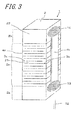
piezoelectric element 1, it is preferable that, as shown inFig. 3 , a bonded region of theexternal electrode conductor layer 5a, 5b in an area near another end opposite to the feeding end, is covered with aresin 14. Thereby, the bonded region positioned near the opposite end which is prone to separation also becomes resistant to separation by virtue of improved heat-accumulation capability and adherability, wherefore the longevity can be increased even further. - In this case, the bonded regions of the
external electrode conductor layer 5a, 5b are covered with theresin 13 and theresin 14, respectively, whereas any regions other than the bonded regions of theexternal electrode conductor layer 5a, 5b are not covered with theresin 13 as well as theresin 14. This makes it possible to suppress damage or separation of theexternal electrode stacked body 2. - Moreover, in the multi-layer
piezoelectric element 1, theresin inactive section 2b which includes stackedpiezoelectric bodies 21 but does not include theinternal electrodes inactive section 2b of poor thermal conductivity). In this case, the resin is capable of producing better heat-accumulation effect (heat-absorption effect) in theinactive section 2b insensitive to an instantaneous temperature change, wherefore the longevity can be increased. Further, since theinactive section 2b does not undergo expansion and contraction, it follows that theresin - Moreover, in the case where the
stacked body 2 is configured to include theactive section 2a in whichpiezoelectric bodies 21 andinternal electrodes inactive sections 2b arranged at both ends of theactive section 2a, each of theinactive section 2b including thepiezoelectric bodies 21, the multi-layerpiezoelectric element 1 can be so designed that theconductor layer 5a, 5b and theexternal electrode active section 2a to theinactive section 2b, and theresin active section 2a and theinactive section 2b. This makes it possible to suppress expansion of theactive section 2a in the vicinity of the interface between theactive section 2a and theinactive section 2b, and thereby lessen the stress occurring at the interface due to the difference in expansion and contraction between theactive section 2a and theinactive section 2b. Accordingly, the longevity can be increased even further. - Further, as shown in
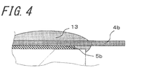
Fig. 4 , in the multi-layerpiezoelectric element 1, in the case where theexternal electrode stacked body 2, it is preferable that part of the end face of thestacked body 2 and part of the protrusion of theexternal electrode resin resin external electrode external electrode - In addition, as shown in
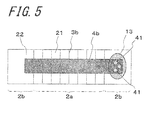
Fig. 5 , the multi-layerpiezoelectric element 1 is configured to form the bonded end portion of theexternal electrode hole 41, thehole 41 being filled with theresin 13. Note thatFig. 5 is a plan view illustrating theexternal electrode 4b-bearing surface of the construction as a top surface, assuming that theresin 13 is transparent. It is preferable that a diameter of thehole 41 is from 0.1 to 1 mm, the number of thehole 41 is from 1 to 10, and the spacing between theadjacent holes 41 is from 0.1 to 0.5 mm from the standpoints of strength enhancement and electric conduction. According to this structure, the volume of the resin and the area of contact between the resin and the external electrode can be increased, with a consequent increase in the amount of heat accumulation (the amount of heat absorption). Moreover, cross-linkage between upper and lower resins can be increased, with a consequent increase in the strength of adhesion between the external electrode and the conductor layer. This makes it possible to suppress damage or separation of the external electrode, and thereby increase the longevity. - Next, a method for manufacturing the multi-layer
piezoelectric element 1 in accordance with one embodiment of the invention will be described. First, for example, powder of PZT (lead zirconate titanate), a binder made of organic high polymer such as acrylic polymer or butyral polymer, and a plasticizer such as DBP (dibutyl phthalate) or DOP (dioctyl phthalate) are mixed to prepare a slurry. - Subsequently, the slurry thus prepared is shaped into ceramic green sheets by a tape molding technique such as the doctor blade method or calender roll method.
- Next, an electrically conducting paste for forming the
internal electrodes internal electrode - Next, a primary stacked compact is obtained by stacking the ceramic green sheets having the printed electrically conducting paste on top of each other in a configuration of, for example, the
active section 2a as shown inFig. 1 with subsequent drying process. Then, a stack of a plurality of printed electrically conducting paste-free ceramic green sheets for constituting theinactive sections 2b are placed at both ends in the stacking direction of the primary stacked compact. In this way, a stacked compact is prepared. Note that the stacked compact can be cut along the stacking direction to obtain a desired shape on an as needed basis. - Next, the stacked compact is subjected to binder removal treatment at a predetermined temperature, and is whereafter fired at a temperature in a range of 900 to 1150°C. In this way, a
stacked body 2 in the form of a column is obtained. It is possible to grind the side surface of thestacked body 2 on an as needed basis. - Next, the
conductor layer 5a, 5b is disposed on the side surface of thestacked body 2. Theconductor layer 5a, 5b can be formed by preparing an electrically conducting paste by admixing a binder, a plasticizer, glass powder, and so forth in metal powder composed predominantly of silver, printing the electrically conducting paste onto the side surface of thestacked body 2 by means of screen printing or otherwise, and performing firing at a temperature in a range of 600 to 800°C. Moreover, a plate-like or mesh-patternedexternal electrode conductor layer 5a, 5b for connection with an external power source. Theexternal electrode - After that, a lead is connected to the
external electrode piezoelectric element 1 of the invention is obtained. - By the manufacturing method thus far described, it is possible to obtain the multi-layer piezoelectric element which suppresses breakage of the external electrode and improves durability.
-
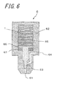
Fig. 6 is a schematic sectional view showing an injection device in accordance with one embodiment of the invention. As shown inFig. 6 , aninjection device 6 of this embodiment includes ahousing 62 including aninjection hole 61 at one end thereof and the above-described multi-layerpiezoelectric element 1 placed within thehousing 62. In an interior of thehousing 62 is disposed aneedle valve 63 capable of opening and closing of theinjection hole 61 by driving the multi-layerpiezoelectric element 1. Afuel passage 64 is so disposed as to be capable of communicating with theinjection hole 61 in accordance with the movement of theneedle valve 63. Thefuel passage 64 is coupled to an external fuel supply source, so that a fuel is supplied to thefuel passage 64 under high pressure at all times. Therefore, when theneedle valve 63 is operated to open theinjection hole 61, then a fuel which has been fed through thefuel passage 64 is injected to a fuel chamber of an internal combustion engine (not shown) with constant high pressure. - Further, an upper end of the
needle valve 63 is apiston 66 which can slide along acylinder 65 which has an increased inner diameter and is provided in thehousing 62. Furthermore, the above-described multi-layerpiezoelectric element 1 is placed within thehousing 62 in contact with thepiston 66. - In the
injection device 6 thus constructed, upon extension of the multi-layerpiezoelectric element 1 entailed by application of voltage, thepiston 66 is pushed forward, thus causing theneedle valve 63 to close theinjection hole 61 with a consequent halt on supply of fuel. Further, upon stopping the application of voltage, the multi-layerpiezoelectric element 1 is contracted, and adisc spring 67 pushes thepiston 66 backward. In consequence, theinjection hole 61 communicates with thefuel passage 64 so that injection of fuel is carried out. - It is noted that the
injection device 6 may include a housing provided with aninjection hole 61 and the multi-layerpiezoelectric element 1, a fluid stored in thehousing 62 being injected through the injection hole by driving the multi-layerpiezoelectric element 1. That is, the multi-layerpiezoelectric element 1 does not necessarily have to be placed within thehousing 62. It is sufficient only that a pressure for control of fluid injection is applied to the interior of thehousing 62 by driving the multi-layerpiezoelectric element 1. In this embodiment, the term "fluid" is construed as encompassing not only fuel and ink, but also various liquid fluid (such as a conductive paste). -
Fig. 7 is a schematic diagram showing the fuel injection system according to an embodiment of the invention. As shown inFig. 7 , afuel injection system 7 according to the embodiment of the invention includes acommon rail 71 configured to store a high-pressure fuel, a plurality ofinjection devices 6 each configured to inject a high-pressure fuel stored in thecommon rail 71, apressure pump 72 configured to supply the high-pressure fuel to thecommon rail 71, and aninjection control unit 73 configured to send a drive signal to theinjection device 6. - The
injection control unit 73 controls an amount of injection of the high-pressure fuel and timing of fuel injection while detecting the condition of the interior of the combustion chamber of an engine by a sensor or the like. Thepressure pump 72 plays a role of supplying a fuel from afuel tank 74 to thecommon rail 71 under pressure of about 1000 to 2000 atmospheres (about 101 MPa to about 203 MPa), and preferably pressure of about 1500 to 1700 atmospheres (about 152 MPa to about 172 MPa). Thecommon rail 71 stores therein the fuel from thepressure pump 72 and acts to feed it to theinjection device 6 on an as needed basis. Theinjection device 6 injects a small amount of fuel into the combustion chamber through theinjection hole 61, as mentioned above. - When using the
fuel injection system 7 of this embodiment, it is possible to stably inject the high pressure fuel as desired for a longer period of time than the case of a conventional fuel injection system. - Hereinafter, practical examples of the multi-layer piezoelectric element of the invention will be described.
- To begin with, a slurry was prepared by mixing calcined powder of piezoelectric ceramic composed predominantly of PZT, a binder made of organic high polymer, and a plasticizer. The slurry was shaped into 150 µm-thick ceramic green sheets by the slip casting technique.
- Then, powder of a silver-palladium alloy having a silver content of 70% by mass and a palladium content of 30% by mass was printed, in a desired pattern with a thickness of 5 µm, onto one side of the ceramic green sheet by screen printing, thereby forming an electrically-conducting paste layer.
- Next, after the electrically-conducting paste layer was dried, 100 ceramic green sheets having the coating of the electrically-conducting paste layer were stacked on top of each other to form a primary stacked compact. In addition, a stack of 20 electrically-conducting paste layer-free ceramic green sheets was placed at the upper end in the stacking direction of the primary stacked compact, and also a stack of 20 electrically-conducting paste layer-free ceramic green sheets was placed at the lower end in the stacking direction of the primary stacked compact. In this way, a stacked compact was formed.
- Next, the stacked compact was subjected to pressure while being heated at a temperature of 100°C to render the ceramic green sheets constituting the stacked compact integral with one another.
- Next, after the stacked compact was cut into a 18 mm-long rectangular prism having a square cross section of a dimension of 8 mm by 8 mm, binder removal treatment was carried out for 10 hours at a temperature of 800°C, and also firing was carried out for 2 hours at a temperature of 1130°C. In this way, a stacked body was obtained. An MgO-made bowl having a hermetic structure was used as a firing bowl in the firing, and ceramic powder having the same composition as the stacked compact and the ceramic included in the stacked compact was put in the bowl with subsequent firing to obtain the stacked body. Note that, in the stacked body, the thickness of piezoelectric body constituting the active section and the inactive sections was set at 100 µm.
- Next, each of the four side surfaces of the stacked body was ground by a thickness of 0.2 mm at a time by a surface grinder. At this time, the grinding was performed so that the ends of the internal electrodes can be exposed alternately at two side surfaces of the stacked body; that is, the end of the
internal electrode 3a can be exposed at theexternal electrode 4a-side side surface of the stacked body, whereas the end of theinternal electrode 3b can be exposed at theexternal electrode 4b-side side surface of the stacked body. Then, an electrically conducting paste composed of an admixture of silver, a binder, a plasticizer, and glass powder was printed onto the side surface of the stacked body by screen printing with subsequent firing at a temperature in the range of 600 to 800°C. In this way, a conductor layer was formed. Moreover, the conductor layer was, at its outer surface, bonded to the SUS-made plate-likeexternal electrode - After that, a lead was connected to the external electrode by solder, and then epoxy-based resin, as well as silicone-based resin, was applied to the bonded end portion of the external electrode bonded to the conductor layer by a dispenser in conformity with the standard listed in Table 1 with subsequent curing for 1 hour at a temperature of 200°C. In this way, multi-layer
piezoelectric elements 1 were obtained. - Lastly, a polarization voltage of 2 kV/mm was applied to the multi-layer piezoelectric element to initiate polarization in the piezoelectric bodies as a whole constituting the multi-layer piezoelectric element. In this way, a multi-layer piezoelectric element according to the invention was obtained.
- Where the item of "Presence of resin at bonded end portion" listed in Table 1 is concerned, the term "Absent" indicates that no resin exists; "Only lead-connected end" indicates that resin exists only at the bonded region of the external electrode which is bonded to the conductor layer in the area near one end (feeding end); and "Both ends" indicates that resin exists at the opposite bonded regions in the stacking direction of the external electrode bonded to the conductor layer.
- Moreover, where the item of "Application position" listed in Table 1 is concerned, the term "Inactive section" indicates that resin exists on the inactive section; "Active section-inactive section interface" indicates that resin lies across the active section and the inactive section; and "Beyond end" indicates that part of the end face of the stacked body and part of the protrusion of the external electrode are bonded to each other by resin.
- Further, where the item of "External electrode" listed in Table 1 is concerned, the term "SUS plate with slits" means a SUS-made external electrode having a number of alternating slits formed so as to extend from their respective long sides of the external electrode toward the center thereof, with the tips of the slits disposed in overlapping relation when viewed in the stacking direction of the stacked body; and "SUS plate with slits and holes" means a SUS-made external electrode having, in addition to slits, holes that are each formed in the location between the overlapping tips of the slits when viewed in the stacking direction so as to extend along the longitudinal axis of the slit. Moreover, when the external electrode was bonded with the conductor layer by an electrically conducting adhesive, there was no special indication, whereas when the external electrode was bonded to the conductor layer by solder, the term "soldered" was indicated.
- The multi-layer piezoelectric elements thus obtained have each been subjected to application of DC voltage of 200 V. The result showed that each of the multi-layer piezoelectric elements underwent displacement of 10 µm (initial displacement) due to expanding and contracting behavior in driving operation. In the measurement of displacement, with each sample held in place on a vibration-proof table, aluminum foil was stuck on the top surface of the sample. Then, the element was measured at its three positions, namely the center and the opposite ends, by a laser displacement gage. The mean value of the amounts of displacement at the three positions was defined as the displacement of the multi-layer piezoelectric element.
- Moreover, a driving test was conducted on each of the multi-layer piezoelectric elements under conditions of application of alternating electric fields of 0 V to +200 V at a frequency of 200 Hz and a temperature of 180°C. In the driving test, following the completion of 1 × 10⁹ cycles of continuous driving operation of the multi-layer piezoelectric element, displacement measurement was conducted to examine a change from the initial displacement. More specifically, there were prepared 10 test pieces per sample for evaluation. The one that exceeded 0.5 µm in respect of the absolute value of displacement change was judged as defective, and the number of defective pieces was counted.
- It is noted that, as a comparative example, there was formed a multi-layer piezoelectric element in which no resin was applied to the bonded end portions of the external electrode bonded to the conductor layer (Sample No. 1). In the same manner as in the multi-layer piezoelectric elements of Sample Nos. 2 through 7, the measurement of initial displacement and the driving test were performed on Sample No. 1.
[Table 1] Sample No. Presence of resin at bonded end portion Type of resin Application position External electrode plate Displacement evaluation after 1 x 10⁹ cycles *1 Absent - - SUS plate with slits 10/10 2 Only lead-connected end Epoxy Inactive section SUS plate with slits 1/10 3 Both ends Epoxy Inactive section SUS plate with slits 0/10 4 Both ends Silicone Inactive section SUS plate with slits 1/10 5 Both ends Epoxy Active section-inactive section interface SUS plate with slits 0/10 6 Both ends Epoxy Beyond end SUS plate with slits 0/10 7 Both ends Epoxy Inactive section SUS plate with slits and holes 0/10 8 Both ends Epoxy Inactive section SUS plate with slits (soldered) 0/10 9 Both ends Epoxy Inactive section SUS plate with slits 0/10 Asterisk (*) indicates sample out of scope of the invention - It has been found that, in each of the multi-layer piezoelectric elements of Sample Nos. 2 through 7 of the invention, none of the 10 test pieces exceeded 0.5 µm in respect of the absolute value of difference between the initial displacement and the displacement as observed after 1 × 10⁹ cycles of continuous driving operation.
- By contrast, it has been found that the multi-layer piezoelectric element of Sample No. 1 suffered from damage to the connected portion of the external electrode due to heat generation.
- It should be noted that the invention is not limited to the embodiments and examples as described hereinabove, and therefore various changes and modifications may be made without departing from the gist of the invention.
-
- 1:
- Multi-layer piezoelectric element
- 12:
- Lead pin
- 13, 14:
- Resin
- 2:
- Stacked body
- 2a:
- Active section
- 2b:
- Inactive section
- 21, 22:
- Piezoelectric body
- 3a, 3b:
- Internal electrode
- 4a, 4b:
- External electrode
- 5a, 5b:
- Conductor layer
Claims (11)
- A multi-layer piezoelectric element, comprising:a stacked body including stacked piezoelectric bodies and internal electrodes;a conductor layer disposed coveringly on a side surface of the stacked body so as to be elongated in a stacking direction of the stacked body to electrically connect with ends of the internal electrodes, which are extended to the side surface of the stacked body; andan external electrode disposed on the conductor layer,one end in the stacking direction of the external electrode being a feeding end,a bonded region of the external electrode, which is bonded to the conductor layer in an area near the feeding end, being covered with a resin.
- The multi-layer piezoelectric element according to claim 1, wherein a bonded region of the external electrode, which is bonded to the conductor layer in an area near another end opposite to the feeding end, is covered with a resin.
- The multi-layer piezoelectric element according to claim 1 or 2, wherein the stacked body is configured to include an active section in which piezoelectric bodies and internal electrodes are alternately laminated, and inactive sections arranged at both ends of the active section, each of inactive sections comprising piezoelectric bodies, and
the conductor layer and the external electrode are each extended from the active section to the inactive sections, and the resin is disposed at the inactive sections. - The multi-layer piezoelectric element according to claim 1 or 2, wherein the stacked body is configured to include an active section in which piezoelectric bodies and internal electrodes are alternately laminated, and inactive sections arranged at both ends of the active section, each of the inactive sections including piezoelectric bodies, and
the conductor layer and the external electrode are each extended from the active section to the inactive sections, and the resin lies across the active section and the inactive sections. - The multi-layer piezoelectric element according to any one of claims 1 to 4, wherein the external electrode is so disposed as to have a protrusion on its feeding-end side, the protrusion extending beyond an end face of the stacked body, and
part of the end face of the stacked body and part of the protrusion of the external electrode are bonded to each other by the resin. - The multi-layer piezoelectric element according to any one of claims 1 to 5, wherein the resin is an epoxy-based resin.
- The multi-layer piezoelectric element according to any one of claims 1 to 6, wherein the bonded region of the external electrode is provided with a hole, the hole being filled with the resin.
- The multi-layer piezoelectric element according to any one of claims 1 to 7, wherein the external electrode is bonded to the conductor layer via an electrically conducting resin.
- The multi-layer piezoelectric element according to any one of claims 1 to 8, wherein the feeding end of the external electrode is covered with the resin.
- An injection device, comprising:a container provided with an injection hole; andthe multi-layer piezoelectric element according to any one of claims 1 to 9,a fluid stored in the container being injected through the injection hole by driving the multi-layer piezoelectric element.
- A fuel injection system comprising:a common rail configured to store a high-pressure fuel;the injection device according to claim 10, the injection device being configured to inject the high-pressure fuel stored in the common rail;a pressure pump configured to supply the high-pressure fuel to the common rail; andan injection control unit configured to send a drive signal to the injection device.
Applications Claiming Priority (2)
| Application Number | Priority Date | Filing Date | Title |
|---|---|---|---|
| JP2010242102 | 2010-10-28 | ||
| PCT/JP2011/074956 WO2012057327A1 (en) | 2010-10-28 | 2011-10-28 | Laminated piezoelectric element, injection device using same, and fuel injection system |
Publications (3)
| Publication Number | Publication Date |
|---|---|
| EP2634827A1 true EP2634827A1 (en) | 2013-09-04 |
| EP2634827A4 EP2634827A4 (en) | 2016-04-13 |
| EP2634827B1 EP2634827B1 (en) | 2020-10-14 |
Family
ID=45994029
Family Applications (1)
| Application Number | Title | Priority Date | Filing Date |
|---|---|---|---|
| EP11836460.3A Active EP2634827B1 (en) | 2010-10-28 | 2011-10-28 | Laminated piezoelectric element, injection device using same, and fuel injection system |
Country Status (5)
| Country | Link |
|---|---|
| US (1) | US9353714B2 (en) |
| EP (1) | EP2634827B1 (en) |
| JP (1) | JP5465337B2 (en) |
| CN (1) | CN103098251B (en) |
| WO (1) | WO2012057327A1 (en) |
Cited By (1)
| Publication number | Priority date | Publication date | Assignee | Title |
|---|---|---|---|---|
| EP3174112A4 (en) * | 2014-07-22 | 2018-04-04 | Kyocera Corporation | Laminated piezoelectric element, injection device provided with laminated piezoelectric element, and fuel injection system provided with laminated piezoelectric element |
Families Citing this family (13)
| Publication number | Priority date | Publication date | Assignee | Title |
|---|---|---|---|---|
| JP5842635B2 (en) * | 2012-01-27 | 2016-01-13 | Tdk株式会社 | Multilayer piezoelectric element |
| ES2903049T3 (en) | 2012-07-25 | 2022-03-30 | Prec Planting Llc | System and method for control and monitoring of multiple row agricultural implements |
| JP5591292B2 (en) * | 2012-09-14 | 2014-09-17 | Tdk株式会社 | Piezoelectric unit |
| DE102012109250B4 (en) * | 2012-09-28 | 2020-07-16 | Tdk Electronics Ag | Electrical component and method for producing contacting of an electrical component |
| JP6086742B2 (en) * | 2013-01-29 | 2017-03-01 | オリンパス株式会社 | Ultrasonic vibration device and ultrasonic medical device |
| EP3101702B1 (en) * | 2014-01-29 | 2020-03-18 | Kyocera Corporation | Laminated piezoelectric element, and injection device and fuel injection system provided with same |
| JP5915703B2 (en) * | 2014-02-27 | 2016-05-11 | Tdk株式会社 | Piezoelectric element unit and driving device |
| JP5724120B1 (en) * | 2014-02-27 | 2015-05-27 | Tdk株式会社 | Piezoelectric element unit and driving device |
| US9293683B2 (en) * | 2014-05-12 | 2016-03-22 | Panasonic Intellectual Property Management Co., Ltd. | Method for connecting piezoelectric element and cable substrate, piezoelectric element having cable substrate, and inkjet head including piezoelectric element with cable substrate |
| JP5971286B2 (en) * | 2014-07-29 | 2016-08-17 | Tdk株式会社 | Lens drive device |
| JP1564966S (en) * | 2016-05-02 | 2016-12-12 | ||
| JP6828331B2 (en) * | 2016-09-09 | 2021-02-10 | Tdk株式会社 | Piezoelectric drive |
| WO2019107558A1 (en) * | 2017-11-30 | 2019-06-06 | 住友理工株式会社 | Transducer and method for manufacturing same |
Family Cites Families (25)
| Publication number | Priority date | Publication date | Assignee | Title |
|---|---|---|---|---|
| JPH01287977A (en) * | 1988-05-13 | 1989-11-20 | Tokin Corp | Piezoelectric actuator |
| JPH03270283A (en) | 1990-03-20 | 1991-12-02 | Fuji Electric Co Ltd | Laminated piezo-electric element |
| JPH04151884A (en) | 1990-10-16 | 1992-05-25 | Fujitsu Ltd | Multilayer piezoelectric device |
| JPH053351A (en) | 1991-06-26 | 1993-01-08 | Nec Corp | Electrostrictive effect element |
| JP2525528B2 (en) | 1991-11-19 | 1996-08-21 | 富士通株式会社 | Piezoelectric actuator |
| DE10042893A1 (en) * | 1999-08-31 | 2001-04-26 | Kyocera Corp | Laminated piezoelectric control element e.g. for optical arrangement, has alternating piezoelectric, inner electrode layers, outer electrodes in sides, top and bottom inactive ceramic layers and insulating blocks |
| JP2001069771A (en) * | 1999-08-31 | 2001-03-16 | Kyocera Corp | Laminated piezoelectric actuator |
| EP1143534B1 (en) * | 2000-03-29 | 2004-05-26 | Nec Tokin Ceramics Corporation | Multilayer piezoelectric actuator with electrodes reinforced in conductivity |
| US6653762B2 (en) | 2000-04-19 | 2003-11-25 | Murata Manufacturing Co., Ltd. | Piezoelectric type electric acoustic converter |
| JP4158338B2 (en) | 2000-06-06 | 2008-10-01 | 株式会社デンソー | Piezoelectric element for injector |
| JP3900918B2 (en) | 2001-12-10 | 2007-04-04 | 株式会社デンソー | Piezoelectric actuator |
| JP2005183478A (en) * | 2003-12-16 | 2005-07-07 | Ibiden Co Ltd | Stacked piezo-electric element |
| WO2005093866A1 (en) * | 2004-03-29 | 2005-10-06 | Kyocera Corporation | Multilayer piezoelectric element and its manufacturing method |
| JP2006041279A (en) | 2004-07-28 | 2006-02-09 | Denso Corp | Laminated piezoelectric element and its manufacturing method |
| JP4299807B2 (en) * | 2005-05-16 | 2009-07-22 | 京セラ株式会社 | Multilayer piezoelectric element and injection device |
| JP4864899B2 (en) | 2005-10-28 | 2012-02-01 | 京セラ株式会社 | Multilayer piezoelectric element and jetting apparatus using the same |
| JP4954897B2 (en) * | 2005-11-29 | 2012-06-20 | 京セラ株式会社 | Multilayer electronic component and manufacturing method thereof |
| JP5135679B2 (en) * | 2005-11-30 | 2013-02-06 | 株式会社村田製作所 | Manufacturing method of multilayer piezoelectric element |
| JP2007173320A (en) * | 2005-12-19 | 2007-07-05 | Denso Corp | Laminate piezoelectric element and its manufacturing method |
| JP2008167548A (en) * | 2006-12-27 | 2008-07-17 | Denso Corp | Piezoelectric actuator |
| DE102008007202A1 (en) | 2008-02-01 | 2009-08-06 | Robert Bosch Gmbh | Piezo actuator module for use with piezo injector, has piezo actuator that is enclosed with coating made of resin material and metal cover, where oxidation gas is inserted or introduced in area |
| CN201434962Y (en) * | 2008-05-02 | 2010-03-31 | 泉株式会社 | Movable type projecting screen device |
| CN102132432A (en) * | 2008-08-26 | 2011-07-20 | 京瓷株式会社 | Multilayer piezoelectric element, injection device using same and fuel injection system |
| JP5342846B2 (en) * | 2008-10-15 | 2013-11-13 | 京セラ株式会社 | Multilayer piezoelectric element, injection device including the same, and fuel injection system |
| WO2010110291A1 (en) * | 2009-03-25 | 2010-09-30 | 京セラ株式会社 | Layered piezoelectric element, injection device utilizing same, and fuel injection system |
-
2011
- 2011-10-28 EP EP11836460.3A patent/EP2634827B1/en active Active
- 2011-10-28 CN CN201180040867.4A patent/CN103098251B/en active Active
- 2011-10-28 WO PCT/JP2011/074956 patent/WO2012057327A1/en active Application Filing
- 2011-10-28 JP JP2012540964A patent/JP5465337B2/en active Active
- 2011-10-28 US US13/880,264 patent/US9353714B2/en active Active
Cited By (2)
| Publication number | Priority date | Publication date | Assignee | Title |
|---|---|---|---|---|
| EP3174112A4 (en) * | 2014-07-22 | 2018-04-04 | Kyocera Corporation | Laminated piezoelectric element, injection device provided with laminated piezoelectric element, and fuel injection system provided with laminated piezoelectric element |
| US10247152B2 (en) | 2014-07-22 | 2019-04-02 | Kyocera Corporation | Multi-layer piezoelectric element, and injection device and fuel injection system provided with the multi-layer piezoelectric element |
Also Published As
| Publication number | Publication date |
|---|---|
| US9353714B2 (en) | 2016-05-31 |
| EP2634827A4 (en) | 2016-04-13 |
| EP2634827B1 (en) | 2020-10-14 |
| US20130233278A1 (en) | 2013-09-12 |
| CN103098251A (en) | 2013-05-08 |
| CN103098251B (en) | 2015-04-01 |
| JPWO2012057327A1 (en) | 2014-05-12 |
| WO2012057327A1 (en) | 2012-05-03 |
| JP5465337B2 (en) | 2014-04-09 |
Similar Documents
| Publication | Publication Date | Title |
|---|---|---|
| EP2634827B1 (en) | Laminated piezoelectric element, injection device using same, and fuel injection system | |
| EP2461385B1 (en) | Multi-layer piezoelectric element, and injection device and fuel injection system using the same | |
| EP2680335B1 (en) | Laminated piezoelectric element, injection apparatus provided with same, and fuel injection system provided with same | |
| EP1675190B1 (en) | Multilayer piezoelectric device | |
| EP2511968B1 (en) | Stacked piezoelectric element, injection device using same, and fuel injection system | |
| EP2495776B1 (en) | Multilayered piezoelectric element and injection device and fuel injection system using the same | |
| EP2667425B1 (en) | Laminated-type piezoelectric element, and piezoelectric actuator, injection apparatus, and fuel injection system provided with same | |
| EP2405503B1 (en) | Laminated piezoelectric element, jetting device provided with same, and fuel jetting system | |
| EP2530756A1 (en) | Laminated piezoelectric element, manufacturing method of same, injection device provided with laminated piezoelectric element, and fuel injection system | |
| EP1686633B1 (en) | Multilayer piezoelectric device | |
| JP5787547B2 (en) | Multilayer piezoelectric element, injection device including the same, and fuel injection system | |
| JP3730893B2 (en) | LAMINATED PIEZOELECTRIC ELEMENT, ITS MANUFACTURING METHOD, AND INJECTION DEVICE | |
| EP2889926B1 (en) | Laminated piezoelectric element, piezoelectric actuator provided with same, injection apparatus, and fuel injection system | |
| EP3174112B1 (en) | Multi-layer piezoelectric element, and injection device and fuel injection system provided with the multi-layer piezoelectric element | |
| JP5701397B2 (en) | Multilayer piezoelectric element, piezoelectric actuator including the same, injection device, and fuel injection system | |
| EP2882003B1 (en) | Laminated piezoelectric element and fuel injection device equipped with same, and fuel injection system |
Legal Events
| Date | Code | Title | Description |
|---|---|---|---|
| PUAI | Public reference made under article 153(3) epc to a published international application that has entered the european phase |
Free format text: ORIGINAL CODE: 0009012 |
|
| 17P | Request for examination filed |
Effective date: 20130528 |
|
| AK | Designated contracting states |
Kind code of ref document: A1 Designated state(s): AL AT BE BG CH CY CZ DE DK EE ES FI FR GB GR HR HU IE IS IT LI LT LU LV MC MK MT NL NO PL PT RO RS SE SI SK SM TR |
|
| DAX | Request for extension of the european patent (deleted) | ||
| RA4 | Supplementary search report drawn up and despatched (corrected) |
Effective date: 20160311 |
|
| RIC1 | Information provided on ipc code assigned before grant |
Ipc: H01L 41/187 20060101ALI20160307BHEP Ipc: H01L 41/293 20130101ALI20160307BHEP Ipc: H01L 41/047 20060101ALI20160307BHEP Ipc: H01L 41/08 20060101ALI20160307BHEP Ipc: H01L 41/22 20060101ALI20160307BHEP Ipc: F02M 51/06 20060101ALI20160307BHEP Ipc: H01L 41/083 20060101AFI20160307BHEP |
|
| STAA | Information on the status of an ep patent application or granted ep patent |
Free format text: STATUS: EXAMINATION IS IN PROGRESS |
|
| 17Q | First examination report despatched |
Effective date: 20180822 |
|
| GRAP | Despatch of communication of intention to grant a patent |
Free format text: ORIGINAL CODE: EPIDOSNIGR1 |
|
| STAA | Information on the status of an ep patent application or granted ep patent |
Free format text: STATUS: GRANT OF PATENT IS INTENDED |
|
| INTG | Intention to grant announced |
Effective date: 20200227 |
|
| GRAJ | Information related to disapproval of communication of intention to grant by the applicant or resumption of examination proceedings by the epo deleted |
Free format text: ORIGINAL CODE: EPIDOSDIGR1 |
|
| STAA | Information on the status of an ep patent application or granted ep patent |
Free format text: STATUS: EXAMINATION IS IN PROGRESS |
|
| INTC | Intention to grant announced (deleted) | ||
| GRAR | Information related to intention to grant a patent recorded |
Free format text: ORIGINAL CODE: EPIDOSNIGR71 |
|
| GRAS | Grant fee paid |
Free format text: ORIGINAL CODE: EPIDOSNIGR3 |
|
| STAA | Information on the status of an ep patent application or granted ep patent |
Free format text: STATUS: GRANT OF PATENT IS INTENDED |
|
| GRAA | (expected) grant |
Free format text: ORIGINAL CODE: 0009210 |
|
| STAA | Information on the status of an ep patent application or granted ep patent |
Free format text: STATUS: THE PATENT HAS BEEN GRANTED |
|
| AK | Designated contracting states |
Kind code of ref document: B1 Designated state(s): AL AT BE BG CH CY CZ DE DK EE ES FI FR GB GR HR HU IE IS IT LI LT LU LV MC MK MT NL NO PL PT RO RS SE SI SK SM TR |
|
| INTG | Intention to grant announced |
Effective date: 20200904 |
|
| REG | Reference to a national code |
Ref country code: GB Ref legal event code: FG4D |
|
| REG | Reference to a national code |
Ref country code: AT Ref legal event code: REF Ref document number: 1324440 Country of ref document: AT Kind code of ref document: T Effective date: 20201015 Ref country code: CH Ref legal event code: EP |
|
| REG | Reference to a national code |
Ref country code: DE Ref legal event code: R096 Ref document number: 602011068964 Country of ref document: DE |
|
| REG | Reference to a national code |
Ref country code: IE Ref legal event code: FG4D |
|
| REG | Reference to a national code |
Ref country code: AT Ref legal event code: MK05 Ref document number: 1324440 Country of ref document: AT Kind code of ref document: T Effective date: 20201014 |
|
| REG | Reference to a national code |
Ref country code: NL Ref legal event code: MP Effective date: 20201014 |
|
| PG25 | Lapsed in a contracting state [announced via postgrant information from national office to epo] |
Ref country code: GR Free format text: LAPSE BECAUSE OF FAILURE TO SUBMIT A TRANSLATION OF THE DESCRIPTION OR TO PAY THE FEE WITHIN THE PRESCRIBED TIME-LIMIT Effective date: 20210115 Ref country code: NL Free format text: LAPSE BECAUSE OF FAILURE TO SUBMIT A TRANSLATION OF THE DESCRIPTION OR TO PAY THE FEE WITHIN THE PRESCRIBED TIME-LIMIT Effective date: 20201014 Ref country code: PT Free format text: LAPSE BECAUSE OF FAILURE TO SUBMIT A TRANSLATION OF THE DESCRIPTION OR TO PAY THE FEE WITHIN THE PRESCRIBED TIME-LIMIT Effective date: 20210215 Ref country code: NO Free format text: LAPSE BECAUSE OF FAILURE TO SUBMIT A TRANSLATION OF THE DESCRIPTION OR TO PAY THE FEE WITHIN THE PRESCRIBED TIME-LIMIT Effective date: 20210114 Ref country code: FI Free format text: LAPSE BECAUSE OF FAILURE TO SUBMIT A TRANSLATION OF THE DESCRIPTION OR TO PAY THE FEE WITHIN THE PRESCRIBED TIME-LIMIT Effective date: 20201014 Ref country code: RS Free format text: LAPSE BECAUSE OF FAILURE TO SUBMIT A TRANSLATION OF THE DESCRIPTION OR TO PAY THE FEE WITHIN THE PRESCRIBED TIME-LIMIT Effective date: 20201014 |
|
| REG | Reference to a national code |
Ref country code: LT Ref legal event code: MG4D |
|
| PG25 | Lapsed in a contracting state [announced via postgrant information from national office to epo] |
Ref country code: SE Free format text: LAPSE BECAUSE OF FAILURE TO SUBMIT A TRANSLATION OF THE DESCRIPTION OR TO PAY THE FEE WITHIN THE PRESCRIBED TIME-LIMIT Effective date: 20201014 Ref country code: LV Free format text: LAPSE BECAUSE OF FAILURE TO SUBMIT A TRANSLATION OF THE DESCRIPTION OR TO PAY THE FEE WITHIN THE PRESCRIBED TIME-LIMIT Effective date: 20201014 Ref country code: PL Free format text: LAPSE BECAUSE OF FAILURE TO SUBMIT A TRANSLATION OF THE DESCRIPTION OR TO PAY THE FEE WITHIN THE PRESCRIBED TIME-LIMIT Effective date: 20201014 Ref country code: BG Free format text: LAPSE BECAUSE OF FAILURE TO SUBMIT A TRANSLATION OF THE DESCRIPTION OR TO PAY THE FEE WITHIN THE PRESCRIBED TIME-LIMIT Effective date: 20210114 Ref country code: AT Free format text: LAPSE BECAUSE OF FAILURE TO SUBMIT A TRANSLATION OF THE DESCRIPTION OR TO PAY THE FEE WITHIN THE PRESCRIBED TIME-LIMIT Effective date: 20201014 Ref country code: IS Free format text: LAPSE BECAUSE OF FAILURE TO SUBMIT A TRANSLATION OF THE DESCRIPTION OR TO PAY THE FEE WITHIN THE PRESCRIBED TIME-LIMIT Effective date: 20210214 Ref country code: ES Free format text: LAPSE BECAUSE OF FAILURE TO SUBMIT A TRANSLATION OF THE DESCRIPTION OR TO PAY THE FEE WITHIN THE PRESCRIBED TIME-LIMIT Effective date: 20201014 |
|
| REG | Reference to a national code |
Ref country code: CH Ref legal event code: PL |
|
| PG25 | Lapsed in a contracting state [announced via postgrant information from national office to epo] |
Ref country code: HR Free format text: LAPSE BECAUSE OF FAILURE TO SUBMIT A TRANSLATION OF THE DESCRIPTION OR TO PAY THE FEE WITHIN THE PRESCRIBED TIME-LIMIT Effective date: 20201014 Ref country code: LU Free format text: LAPSE BECAUSE OF NON-PAYMENT OF DUE FEES Effective date: 20201028 |
|
| REG | Reference to a national code |
Ref country code: DE Ref legal event code: R097 Ref document number: 602011068964 Country of ref document: DE Ref country code: BE Ref legal event code: MM Effective date: 20201031 |
|
| PG25 | Lapsed in a contracting state [announced via postgrant information from national office to epo] |
Ref country code: RO Free format text: LAPSE BECAUSE OF FAILURE TO SUBMIT A TRANSLATION OF THE DESCRIPTION OR TO PAY THE FEE WITHIN THE PRESCRIBED TIME-LIMIT Effective date: 20201014 Ref country code: SK Free format text: LAPSE BECAUSE OF FAILURE TO SUBMIT A TRANSLATION OF THE DESCRIPTION OR TO PAY THE FEE WITHIN THE PRESCRIBED TIME-LIMIT Effective date: 20201014 Ref country code: LT Free format text: LAPSE BECAUSE OF FAILURE TO SUBMIT A TRANSLATION OF THE DESCRIPTION OR TO PAY THE FEE WITHIN THE PRESCRIBED TIME-LIMIT Effective date: 20201014 Ref country code: MC Free format text: LAPSE BECAUSE OF FAILURE TO SUBMIT A TRANSLATION OF THE DESCRIPTION OR TO PAY THE FEE WITHIN THE PRESCRIBED TIME-LIMIT Effective date: 20201014 Ref country code: SM Free format text: LAPSE BECAUSE OF FAILURE TO SUBMIT A TRANSLATION OF THE DESCRIPTION OR TO PAY THE FEE WITHIN THE PRESCRIBED TIME-LIMIT Effective date: 20201014 Ref country code: CZ Free format text: LAPSE BECAUSE OF FAILURE TO SUBMIT A TRANSLATION OF THE DESCRIPTION OR TO PAY THE FEE WITHIN THE PRESCRIBED TIME-LIMIT Effective date: 20201014 Ref country code: EE Free format text: LAPSE BECAUSE OF FAILURE TO SUBMIT A TRANSLATION OF THE DESCRIPTION OR TO PAY THE FEE WITHIN THE PRESCRIBED TIME-LIMIT Effective date: 20201014 |
|
| PLBE | No opposition filed within time limit |
Free format text: ORIGINAL CODE: 0009261 |
|
| STAA | Information on the status of an ep patent application or granted ep patent |
Free format text: STATUS: NO OPPOSITION FILED WITHIN TIME LIMIT |
|
| PG25 | Lapsed in a contracting state [announced via postgrant information from national office to epo] |
Ref country code: LI Free format text: LAPSE BECAUSE OF NON-PAYMENT OF DUE FEES Effective date: 20201031 Ref country code: CH Free format text: LAPSE BECAUSE OF NON-PAYMENT OF DUE FEES Effective date: 20201031 Ref country code: DK Free format text: LAPSE BECAUSE OF FAILURE TO SUBMIT A TRANSLATION OF THE DESCRIPTION OR TO PAY THE FEE WITHIN THE PRESCRIBED TIME-LIMIT Effective date: 20201014 Ref country code: BE Free format text: LAPSE BECAUSE OF NON-PAYMENT OF DUE FEES Effective date: 20201031 |
|
| 26N | No opposition filed |
Effective date: 20210715 |
|
| PG25 | Lapsed in a contracting state [announced via postgrant information from national office to epo] |
Ref country code: IT Free format text: LAPSE BECAUSE OF FAILURE TO SUBMIT A TRANSLATION OF THE DESCRIPTION OR TO PAY THE FEE WITHIN THE PRESCRIBED TIME-LIMIT Effective date: 20201014 Ref country code: IE Free format text: LAPSE BECAUSE OF NON-PAYMENT OF DUE FEES Effective date: 20201028 Ref country code: AL Free format text: LAPSE BECAUSE OF FAILURE TO SUBMIT A TRANSLATION OF THE DESCRIPTION OR TO PAY THE FEE WITHIN THE PRESCRIBED TIME-LIMIT Effective date: 20201014 |
|
| PG25 | Lapsed in a contracting state [announced via postgrant information from national office to epo] |
Ref country code: SI Free format text: LAPSE BECAUSE OF FAILURE TO SUBMIT A TRANSLATION OF THE DESCRIPTION OR TO PAY THE FEE WITHIN THE PRESCRIBED TIME-LIMIT Effective date: 20201014 |
|
| PG25 | Lapsed in a contracting state [announced via postgrant information from national office to epo] |
Ref country code: IS Free format text: LAPSE BECAUSE OF FAILURE TO SUBMIT A TRANSLATION OF THE DESCRIPTION OR TO PAY THE FEE WITHIN THE PRESCRIBED TIME-LIMIT Effective date: 20210214 Ref country code: TR Free format text: LAPSE BECAUSE OF FAILURE TO SUBMIT A TRANSLATION OF THE DESCRIPTION OR TO PAY THE FEE WITHIN THE PRESCRIBED TIME-LIMIT Effective date: 20201014 Ref country code: MT Free format text: LAPSE BECAUSE OF FAILURE TO SUBMIT A TRANSLATION OF THE DESCRIPTION OR TO PAY THE FEE WITHIN THE PRESCRIBED TIME-LIMIT Effective date: 20201014 Ref country code: CY Free format text: LAPSE BECAUSE OF FAILURE TO SUBMIT A TRANSLATION OF THE DESCRIPTION OR TO PAY THE FEE WITHIN THE PRESCRIBED TIME-LIMIT Effective date: 20201014 |
|
| PG25 | Lapsed in a contracting state [announced via postgrant information from national office to epo] |
Ref country code: MK Free format text: LAPSE BECAUSE OF FAILURE TO SUBMIT A TRANSLATION OF THE DESCRIPTION OR TO PAY THE FEE WITHIN THE PRESCRIBED TIME-LIMIT Effective date: 20201014 |
|
| PGFP | Annual fee paid to national office [announced via postgrant information from national office to epo] |
Ref country code: GB Payment date: 20220908 Year of fee payment: 12 |
|
| REG | Reference to a national code |
Ref country code: DE Ref legal event code: R079 Ref document number: 602011068964 Country of ref document: DE Free format text: PREVIOUS MAIN CLASS: H01L0041083000 Ipc: H10N0030500000 |
|
| PGFP | Annual fee paid to national office [announced via postgrant information from national office to epo] |
Ref country code: FR Payment date: 20220908 Year of fee payment: 12 |
|
| P01 | Opt-out of the competence of the unified patent court (upc) registered |
Effective date: 20230505 |
|
| PGFP | Annual fee paid to national office [announced via postgrant information from national office to epo] |
Ref country code: DE Payment date: 20230906 Year of fee payment: 13 |
|
| GBPC | Gb: european patent ceased through non-payment of renewal fee |
Effective date: 20231028 |
|
| PG25 | Lapsed in a contracting state [announced via postgrant information from national office to epo] |
Ref country code: GB Free format text: LAPSE BECAUSE OF NON-PAYMENT OF DUE FEES Effective date: 20231028 |
|
| PG25 | Lapsed in a contracting state [announced via postgrant information from national office to epo] |
Ref country code: GB Free format text: LAPSE BECAUSE OF NON-PAYMENT OF DUE FEES Effective date: 20231028 Ref country code: FR Free format text: LAPSE BECAUSE OF NON-PAYMENT OF DUE FEES Effective date: 20231031 |