JP6828331B2 - Piezoelectric drive - Google Patents
Piezoelectric drive Download PDFInfo
- Publication number
- JP6828331B2 JP6828331B2 JP2016177117A JP2016177117A JP6828331B2 JP 6828331 B2 JP6828331 B2 JP 6828331B2 JP 2016177117 A JP2016177117 A JP 2016177117A JP 2016177117 A JP2016177117 A JP 2016177117A JP 6828331 B2 JP6828331 B2 JP 6828331B2
- Authority
- JP
- Japan
- Prior art keywords
- electrode
- end surface
- shaft
- piezoelectric element
- laminated piezoelectric
- Prior art date
- Legal status (The legal status is an assumption and is not a legal conclusion. Google has not performed a legal analysis and makes no representation as to the accuracy of the status listed.)
- Active
Links
- 239000000853 adhesive Substances 0.000 claims description 45
- 230000001070 adhesive effect Effects 0.000 claims description 45
- 238000009413 insulation Methods 0.000 claims description 7
- 229910052751 metal Inorganic materials 0.000 description 51
- 239000002184 metal Substances 0.000 description 51
- 239000010410 layer Substances 0.000 description 33
- 238000006073 displacement reaction Methods 0.000 description 10
- 238000000034 method Methods 0.000 description 10
- 230000000694 effects Effects 0.000 description 7
- 238000005452 bending Methods 0.000 description 6
- 239000000463 material Substances 0.000 description 5
- 239000004020 conductor Substances 0.000 description 4
- 239000011810 insulating material Substances 0.000 description 4
- 238000007747 plating Methods 0.000 description 3
- 229910000679 solder Inorganic materials 0.000 description 3
- 238000004544 sputter deposition Methods 0.000 description 3
- 238000003466 welding Methods 0.000 description 3
- XEEYBQQBJWHFJM-UHFFFAOYSA-N Iron Chemical compound [Fe] XEEYBQQBJWHFJM-UHFFFAOYSA-N 0.000 description 2
- 229910000831 Steel Inorganic materials 0.000 description 2
- 229910045601 alloy Inorganic materials 0.000 description 2
- 239000000956 alloy Substances 0.000 description 2
- 229910052782 aluminium Inorganic materials 0.000 description 2
- XAGFODPZIPBFFR-UHFFFAOYSA-N aluminium Chemical compound [Al] XAGFODPZIPBFFR-UHFFFAOYSA-N 0.000 description 2
- 239000000919 ceramic Substances 0.000 description 2
- 238000005336 cracking Methods 0.000 description 2
- 238000009792 diffusion process Methods 0.000 description 2
- 238000010304 firing Methods 0.000 description 2
- 230000002093 peripheral effect Effects 0.000 description 2
- 239000004033 plastic Substances 0.000 description 2
- 229920003023 plastic Polymers 0.000 description 2
- 239000010970 precious metal Substances 0.000 description 2
- 230000001681 protective effect Effects 0.000 description 2
- 239000011241 protective layer Substances 0.000 description 2
- 230000004043 responsiveness Effects 0.000 description 2
- 239000007790 solid phase Substances 0.000 description 2
- 239000010959 steel Substances 0.000 description 2
- OKTJSMMVPCPJKN-UHFFFAOYSA-N Carbon Chemical compound [C] OKTJSMMVPCPJKN-UHFFFAOYSA-N 0.000 description 1
- CWYNVVGOOAEACU-UHFFFAOYSA-N Fe2+ Chemical compound [Fe+2] CWYNVVGOOAEACU-UHFFFAOYSA-N 0.000 description 1
- 239000004962 Polyamide-imide Substances 0.000 description 1
- 238000010521 absorption reaction Methods 0.000 description 1
- 239000010953 base metal Substances 0.000 description 1
- 229910052799 carbon Inorganic materials 0.000 description 1
- 229910052802 copper Inorganic materials 0.000 description 1
- 238000005516 engineering process Methods 0.000 description 1
- 229910052737 gold Inorganic materials 0.000 description 1
- 230000005484 gravity Effects 0.000 description 1
- 239000012212 insulator Substances 0.000 description 1
- 229910052742 iron Inorganic materials 0.000 description 1
- 238000005304 joining Methods 0.000 description 1
- 238000004519 manufacturing process Methods 0.000 description 1
- 239000007769 metal material Substances 0.000 description 1
- 150000002739 metals Chemical class 0.000 description 1
- 229910052759 nickel Inorganic materials 0.000 description 1
- 229910052763 palladium Inorganic materials 0.000 description 1
- 229910052697 platinum Inorganic materials 0.000 description 1
- 230000010287 polarization Effects 0.000 description 1
- 229920002312 polyamide-imide Polymers 0.000 description 1
- 239000002990 reinforced plastic Substances 0.000 description 1
- 239000011347 resin Substances 0.000 description 1
- 229920005989 resin Polymers 0.000 description 1
- 229910052709 silver Inorganic materials 0.000 description 1
- 239000010935 stainless steel Substances 0.000 description 1
- 229910001220 stainless steel Inorganic materials 0.000 description 1
- 238000003756 stirring Methods 0.000 description 1
- 239000000758 substrate Substances 0.000 description 1
- WFKWXMTUELFFGS-UHFFFAOYSA-N tungsten Chemical compound [W] WFKWXMTUELFFGS-UHFFFAOYSA-N 0.000 description 1
- 229910052721 tungsten Inorganic materials 0.000 description 1
- 239000010937 tungsten Substances 0.000 description 1
- 239000002699 waste material Substances 0.000 description 1
Images


Classifications
-
- H—ELECTRICITY
- H10—SEMICONDUCTOR DEVICES; ELECTRIC SOLID-STATE DEVICES NOT OTHERWISE PROVIDED FOR
- H10N—ELECTRIC SOLID-STATE DEVICES NOT OTHERWISE PROVIDED FOR
- H10N30/00—Piezoelectric or electrostrictive devices
- H10N30/20—Piezoelectric or electrostrictive devices with electrical input and mechanical output, e.g. functioning as actuators or vibrators
-
- H—ELECTRICITY
- H02—GENERATION; CONVERSION OR DISTRIBUTION OF ELECTRIC POWER
- H02N—ELECTRIC MACHINES NOT OTHERWISE PROVIDED FOR
- H02N2/00—Electric machines in general using piezoelectric effect, electrostriction or magnetostriction
- H02N2/02—Electric machines in general using piezoelectric effect, electrostriction or magnetostriction producing linear motion, e.g. actuators; Linear positioners ; Linear motors
- H02N2/06—Drive circuits; Control arrangements or methods
-
- H—ELECTRICITY
- H02—GENERATION; CONVERSION OR DISTRIBUTION OF ELECTRIC POWER
- H02N—ELECTRIC MACHINES NOT OTHERWISE PROVIDED FOR
- H02N2/00—Electric machines in general using piezoelectric effect, electrostriction or magnetostriction
- H02N2/0005—Electric machines in general using piezoelectric effect, electrostriction or magnetostriction producing non-specific motion; Details common to machines covered by H02N2/02 - H02N2/16
- H02N2/001—Driving devices, e.g. vibrators
- H02N2/002—Driving devices, e.g. vibrators using only longitudinal or radial modes
-
- H—ELECTRICITY
- H02—GENERATION; CONVERSION OR DISTRIBUTION OF ELECTRIC POWER
- H02N—ELECTRIC MACHINES NOT OTHERWISE PROVIDED FOR
- H02N2/00—Electric machines in general using piezoelectric effect, electrostriction or magnetostriction
- H02N2/02—Electric machines in general using piezoelectric effect, electrostriction or magnetostriction producing linear motion, e.g. actuators; Linear positioners ; Linear motors
- H02N2/021—Electric machines in general using piezoelectric effect, electrostriction or magnetostriction producing linear motion, e.g. actuators; Linear positioners ; Linear motors using intermittent driving, e.g. step motors, piezoleg motors
- H02N2/025—Inertial sliding motors
-
- H—ELECTRICITY
- H10—SEMICONDUCTOR DEVICES; ELECTRIC SOLID-STATE DEVICES NOT OTHERWISE PROVIDED FOR
- H10N—ELECTRIC SOLID-STATE DEVICES NOT OTHERWISE PROVIDED FOR
- H10N30/00—Piezoelectric or electrostrictive devices
- H10N30/50—Piezoelectric or electrostrictive devices having a stacked or multilayer structure
-
- H—ELECTRICITY
- H10—SEMICONDUCTOR DEVICES; ELECTRIC SOLID-STATE DEVICES NOT OTHERWISE PROVIDED FOR
- H10N—ELECTRIC SOLID-STATE DEVICES NOT OTHERWISE PROVIDED FOR
- H10N30/00—Piezoelectric or electrostrictive devices
- H10N30/80—Constructional details
- H10N30/802—Circuitry or processes for operating piezoelectric or electrostrictive devices not otherwise provided for, e.g. drive circuits
-
- H—ELECTRICITY
- H10—SEMICONDUCTOR DEVICES; ELECTRIC SOLID-STATE DEVICES NOT OTHERWISE PROVIDED FOR
- H10N—ELECTRIC SOLID-STATE DEVICES NOT OTHERWISE PROVIDED FOR
- H10N30/00—Piezoelectric or electrostrictive devices
- H10N30/80—Constructional details
- H10N30/87—Electrodes or interconnections, e.g. leads or terminals
- H10N30/871—Single-layered electrodes of multilayer piezoelectric or electrostrictive devices, e.g. internal electrodes
-
- H—ELECTRICITY
- H10—SEMICONDUCTOR DEVICES; ELECTRIC SOLID-STATE DEVICES NOT OTHERWISE PROVIDED FOR
- H10N—ELECTRIC SOLID-STATE DEVICES NOT OTHERWISE PROVIDED FOR
- H10N30/00—Piezoelectric or electrostrictive devices
- H10N30/80—Constructional details
- H10N30/87—Electrodes or interconnections, e.g. leads or terminals
- H10N30/872—Interconnections, e.g. connection electrodes of multilayer piezoelectric or electrostrictive devices
-
- B—PERFORMING OPERATIONS; TRANSPORTING
- B60—VEHICLES IN GENERAL
- B60J—WINDOWS, WINDSCREENS, NON-FIXED ROOFS, DOORS, OR SIMILAR DEVICES FOR VEHICLES; REMOVABLE EXTERNAL PROTECTIVE COVERINGS SPECIALLY ADAPTED FOR VEHICLES
- B60J1/00—Windows; Windscreens; Accessories therefor
- B60J1/08—Windows; Windscreens; Accessories therefor arranged at vehicle sides
- B60J1/12—Windows; Windscreens; Accessories therefor arranged at vehicle sides adjustable
- B60J1/16—Windows; Windscreens; Accessories therefor arranged at vehicle sides adjustable slidable
- B60J1/17—Windows; Windscreens; Accessories therefor arranged at vehicle sides adjustable slidable vertically
-
- E—FIXED CONSTRUCTIONS
- E05—LOCKS; KEYS; WINDOW OR DOOR FITTINGS; SAFES
- E05F—DEVICES FOR MOVING WINGS INTO OPEN OR CLOSED POSITION; CHECKS FOR WINGS; WING FITTINGS NOT OTHERWISE PROVIDED FOR, CONCERNED WITH THE FUNCTIONING OF THE WING
- E05F15/00—Power-operated mechanisms for wings
- E05F15/60—Power-operated mechanisms for wings using electrical actuators
-
- G—PHYSICS
- G02—OPTICS
- G02B—OPTICAL ELEMENTS, SYSTEMS OR APPARATUS
- G02B7/00—Mountings, adjusting means, or light-tight connections, for optical elements
- G02B7/02—Mountings, adjusting means, or light-tight connections, for optical elements for lenses
- G02B7/04—Mountings, adjusting means, or light-tight connections, for optical elements for lenses with mechanism for focusing or varying magnification
- G02B7/08—Mountings, adjusting means, or light-tight connections, for optical elements for lenses with mechanism for focusing or varying magnification adapted to co-operate with a remote control mechanism
Landscapes
- General Electrical Machinery Utilizing Piezoelectricity, Electrostriction Or Magnetostriction (AREA)
- Lens Barrels (AREA)
Description
本発明は、たとえばレンズ枠などの移動体をシャフトに沿って移動させるための圧電駆動装置に関する。 The present invention relates to a piezoelectric drive for moving a moving body, such as a lens frame, along a shaft.
積層型圧電素子を用いてレンズ枠を軸方向に駆動するための圧電駆動装置としては、たとえば特許文献1に示すものが知られている。この特許文献1にも示すように、従来の圧電駆動装置では、積層型圧電素子の第1端面に錘部材が接続され、その第1端面と反対側の第2端面にシャフトが接合してある。そして、この圧電素子を駆動することでシャフトに振動を加え、移動体をシャフトの軸方向に移動させている。 As a piezoelectric driving device for driving a lens frame in the axial direction by using a laminated piezoelectric element, for example, the one shown in Patent Document 1 is known. As shown in Patent Document 1, in the conventional piezoelectric drive device, a weight member is connected to the first end surface of the laminated piezoelectric element, and the shaft is joined to the second end surface opposite to the first end surface. .. Then, by driving this piezoelectric element, vibration is applied to the shaft to move the moving body in the axial direction of the shaft.
従来の圧電駆動装置に用いられる積層型圧電素子では、第1端面または第2端面に平行となるように、内部電極および圧電層が交互に積層されることが一般的である。このような方向に内部電極が積層してある積層型圧電素子を用いることで、シャフトに伝える駆動力が大きくなり、移動体を効率的に移動させることができると考えられていた。 In a laminated piezoelectric element used in a conventional piezoelectric drive device, internal electrodes and piezoelectric layers are generally laminated alternately so as to be parallel to the first end surface or the second end surface. It has been considered that by using a laminated piezoelectric element in which internal electrodes are laminated in such a direction, the driving force transmitted to the shaft is increased and the moving body can be efficiently moved.
しかしながら、従来の圧電駆動装置では、第1端面または第2端面に平行となるように、内部電極および圧電層が交互に積層される積層型圧電素子を用いているために、シャフトに横から荷重が作用した場合などに折れやすいという課題を有している。特に、内部電極に平行な平面に沿ってクラックが生じて折れやすい。 However, in the conventional piezoelectric drive device, since the laminated piezoelectric element in which the internal electrodes and the piezoelectric layers are alternately laminated so as to be parallel to the first end surface or the second end surface is used, a load is applied from the side to the shaft. It has a problem that it is easily broken when it acts. In particular, cracks occur along a plane parallel to the internal electrode and are easily broken.
本発明は、このような実状に鑑みてなされ、その目的は、シャフトなどに横から荷重が作用しても積層型圧電素子が折れにくい圧電駆動装置を提供することである。 The present invention has been made in view of such an actual situation, and an object of the present invention is to provide a piezoelectric drive device in which a laminated piezoelectric element is hard to break even when a load is applied to a shaft or the like from the side.
上記目的を達成するために、本発明に係る圧電駆動装置は、
第1端面と、当該第1端面とは反対側に位置する第2端面とを持つ積層型圧電素子と、
前記積層型圧電素子の第1端面に取り付けられる錘部材と、
前記積層型圧電素子の前記第2端面に取り付けられるシャフトと、を有し、
前記積層型圧電素子を駆動することにより、 前記シャフトに対して軸方向に移動自在に係合された移動部材を軸方向に沿って移動させる圧電駆動装置であって、
前記積層型圧電素子の内部では、前記第1端面または前記第2端面に略垂直な平面をそれぞれ持つ第1内部電極および第2内部電極が、圧電層を挟んで、前記第1内部電極および前記第2内部電極に略垂直な方向に向けて積層してあることを特徴とする。
In order to achieve the above object, the piezoelectric drive device according to the present invention is
A laminated piezoelectric element having a first end face and a second end face located on the side opposite to the first end face.
A weight member attached to the first end surface of the laminated piezoelectric element,
It has a shaft attached to the second end surface of the laminated piezoelectric element, and has.
A piezoelectric drive device that moves a moving member movably engaged with the shaft in the axial direction by driving the laminated piezoelectric element.
Inside the laminated piezoelectric element, the first internal electrode and the second internal electrode having a plane substantially perpendicular to the first end surface or the second end surface respectively sandwich the piezoelectric layer, and the first internal electrode and the said It is characterized in that it is laminated in a direction substantially perpendicular to the second internal electrode.
本発明に係る圧電駆動装置では、第1端面または第2端面に略垂直な平面をそれぞれ持つ第1内部電極および第2内部電極が、圧電層を挟んで、第1内部電極および第2内部電極に略垂直な方向に向けて積層してある。このため、シャフトなどに横から荷重が作用しても、その力は、積層型圧電素子の内部では、積層してある複数の内部電極を折り曲げる方向に作用し、内部電極の界面を引き剥がす方向には作用しない。したがって、従来とは異なり、積層型圧電素子の内部での内部電極の積層配列が、素子の折れ曲がりに抵抗する構造となり、素子の折れ曲がりやクラックなどを有効に阻止することができる。 In the piezoelectric drive device according to the present invention, the first internal electrode and the second internal electrode having a plane substantially perpendicular to the first end surface or the second end surface respectively sandwich the piezoelectric layer, and the first internal electrode and the second internal electrode It is laminated in a direction substantially perpendicular to. Therefore, even if a load acts on the shaft or the like from the side, the force acts in the direction of bending the plurality of stacked internal electrodes inside the laminated piezoelectric element, and the direction of peeling off the interface of the internal electrodes. Does not work on. Therefore, unlike the conventional case, the laminated arrangement of the internal electrodes inside the laminated piezoelectric element has a structure that resists the bending of the element, and the bending and cracking of the element can be effectively prevented.
また、本発明に係る圧電駆動装置は、従来の圧電駆動装置とは内部電極の積層方向が異なるために、第1端面から第2端面に向かう方向の共振に強い構造となり、従来よりも高い周波数での使用が可能となる。そのため、シャフトへ変位を与える回数を増大させることが可能になり、応答性が向上する。 Further, since the piezoelectric drive device according to the present invention has a different stacking direction of internal electrodes from the conventional piezoelectric drive device, it has a structure resistant to resonance in the direction from the first end face to the second end face, and has a higher frequency than the conventional one. Can be used in. Therefore, it becomes possible to increase the number of times the displacement is applied to the shaft, and the responsiveness is improved.
さらに、第1内部電極および第2内部電極が、圧電層を挟んで、同一方向に沿って繰り返して配置される単純な構造であるために、焼成時などにもクラックが入りにくい構造であると共に、圧電層の分極も容易である。 Further, since the first internal electrode and the second internal electrode have a simple structure in which the piezoelectric layer is sandwiched between them and are repeatedly arranged along the same direction, the structure is such that cracks are unlikely to occur even during firing. , The polarization of the piezoelectric layer is also easy.
好ましくは、前記第1端面と前記第2端面との間の距離に対応する前記積層型圧電素子の長さは、前記第1内部電極および前記第2内部電極に略垂直な方向に沿った前記積層型圧電素子の積層方向厚みよりも長い。従来では、第1端面と前記第2端面との間の距離を長くすると、第1端面または第2端面に平行な内部電極の積層数が多くなったり、内部電極が積層されていない圧電層の厚みが厚くなり、圧電層の界面に沿って圧電素子が折れやすくなる。 Preferably, the length of the laminated piezoelectric element corresponding to the distance between the first end face and the second end face is along a direction substantially perpendicular to the first internal electrode and the second internal electrode. It is longer than the thickness in the stacking direction of the laminated piezoelectric element. Conventionally, when the distance between the first end face and the second end face is increased, the number of laminated internal electrodes parallel to the first end face or the second end face increases, or the piezoelectric layer in which the internal electrodes are not laminated increases. The thickness becomes thicker, and the piezoelectric element easily breaks along the interface of the piezoelectric layer.
これに対して、本発明では、内部電極の長手方向の長さを長くすることで、第1端面と第2端面との間の距離を長くすることが可能であり、従来に比較して折れにくい構造である。また、内部電極の長手方向の長さを長くすることで、内部電極の面積が大きくなり、内部電極に挟まれる圧電層の体積を大きくすることが可能になり、圧電素子の長手方向の変位を大きくすることができる。 On the other hand, in the present invention, by increasing the length of the internal electrode in the longitudinal direction, it is possible to increase the distance between the first end surface and the second end surface, and the internal electrode is broken as compared with the conventional case. It is a difficult structure. Further, by increasing the length of the internal electrode in the longitudinal direction, the area of the internal electrode is increased, the volume of the piezoelectric layer sandwiched between the internal electrodes can be increased, and the displacement of the piezoelectric element in the longitudinal direction can be increased. It can be made larger.
前記第1内部電極に接続してある第1外部電極と、前記第2内部電極に接続してある第2外部電極とが、前記第1端面および前記第2端面のいずれか一方の近くに位置する前記積層型圧電素子の側面に形成してあることが好ましい。 The first external electrode connected to the first internal electrode and the second external electrode connected to the second internal electrode are located near either the first end surface or the second end surface. It is preferable that it is formed on the side surface of the laminated piezoelectric element.
このように構成することで、積層型圧電素子の第1内部電極および第2内部電極の各々に印加する電圧を加えるための配線を、錘部材またはシャフトのいずれか一方の近傍に具備させれば良く、配線が容易になる。特に、錘部材は固定側に配置されるため、配線が容易である。 With this configuration, if wiring for applying a voltage applied to each of the first internal electrode and the second internal electrode of the laminated piezoelectric element is provided in the vicinity of either the weight member or the shaft. Good and easy to wire. In particular, since the weight member is arranged on the fixed side, wiring is easy.
好ましくは、前記第1端面には、第1接着剤を介して前記錘部材が接着してある。第1端面の近傍に第1外部電極および第2外部電極が配置される場合に、この第1接着剤は、第1外部電極または第2外部電極を外部回路に接続するための接続部材が第1端面に入り込むことを阻止することができる。 Preferably, the weight member is adhered to the first end surface via a first adhesive. When the first external electrode and the second external electrode are arranged in the vicinity of the first end surface, the first adhesive is a connecting member for connecting the first external electrode or the second external electrode to the external circuit. It can be prevented from entering one end face.
また好ましくは、 前記第2端面には、第2接着剤を介して前記シャフトが接着してある。第1端面の近傍に第1外部電極および第2外部電極が配置される場合に、この第2接着剤は、第2端面で露出する可能性がある第1内部電極の端部と第2内部電極の端部との絶縁を確保することができる。 Further, preferably, the shaft is adhered to the second end surface via a second adhesive. When the first external electrode and the second external electrode are arranged in the vicinity of the first end face, this second adhesive is exposed at the end surface of the first internal electrode and the second inside of the second end face. Insulation from the end of the electrode can be ensured.
第2端面の近傍に第1外部電極および第2外部電極が配置される場合には、第1接着剤は、第1端面で露出する可能性がある第1内部電極の端部と第2内部電極の端部との絶縁を確保することができる。また、第2接着剤は、第1外部電極または第2外部電極を外部回路に接続するための接続部材が第2端面に入り込むことを阻止することができる。 When the first external electrode and the second external electrode are arranged in the vicinity of the second end face, the first adhesive is applied to the end portion and the second inside of the first internal electrode which may be exposed on the first end face. Insulation from the end of the electrode can be ensured. In addition, the second adhesive can prevent the connecting member for connecting the first external electrode or the second external electrode to the external circuit from entering the second end surface.
本発明では、第1端面または前記第2端面に略垂直な平面をそれぞれ持つ第1内部電極および第2内部電極が、第1内部電極および第2内部電極に略垂直な方向に向けて積層してある。そのため、第1内部電極および第2内部電極の各端部は、第1端面または第2端面で露出していてもよい。第1接着剤は第1端面を覆い、第2接着剤は第2端面を覆うことになるので、これらの内部電極が露出する端面を各接着剤が有効に保護することができる。なお、第1端面または第2端面には、予め保護絶縁層が形成してあってもよい。 In the present invention, the first internal electrode and the second internal electrode having a plane substantially perpendicular to the first end surface or the second end surface are laminated in a direction substantially perpendicular to the first internal electrode and the second internal electrode. There is. Therefore, each end of the first internal electrode and the second internal electrode may be exposed on the first end surface or the second end surface. Since the first adhesive covers the first end face and the second adhesive covers the second end face, each adhesive can effectively protect the end face where these internal electrodes are exposed. A protective insulating layer may be formed in advance on the first end face or the second end face.
前記第1接着剤は、前記錘部材をフレーム部材の凹部に固定するための部材を兼ねていてもよい。錘部材は、フレーム部材の凹部に固定されることがあるため、その場合に用いられる接着剤を用いて積層型圧電素子の第1端面を錘部材に接着してもよい。 The first adhesive may also serve as a member for fixing the weight member to the recess of the frame member. Since the weight member may be fixed to the recess of the frame member, the first end surface of the laminated piezoelectric element may be adhered to the weight member by using the adhesive used in that case.
前記第1内部電極に接続してある第1外部電極が、前記第1端面に形成してあり、前記第2内部電極に接続してある第2外部電極が、前記第2端面に形成してあってもよい。この場合には、第1外部電極が錘部材の近傍に具備してある第1配線に接続され、第2外部電極がシャフトを介して第2配線に接続されてもよい。 The first external electrode connected to the first internal electrode is formed on the first end surface, and the second external electrode connected to the second internal electrode is formed on the second end surface. There may be. In this case, the first external electrode may be connected to the first wiring provided in the vicinity of the weight member, and the second external electrode may be connected to the second wiring via the shaft.
あるいは、前記第1外部電極は、前記第1端面に形成してある第1端面電極部と、前記第1端面電極部から前記積層型圧電素子の一側面に連続して形成してある第1側面電極部とを有し、
前記第2外部電極は、前記第2端面に形成してある第2端面電極部と、前記第2端面電極から前記積層型圧電素子の他の側面に連続して形成してある第2側面電極部とを有していてもよい。
Alternatively, the first external electrode is formed continuously from the first end surface electrode portion formed on the first end surface and the first end surface electrode portion on one side surface of the laminated piezoelectric element. It has a side electrode part and
The second external electrode includes a second end surface electrode portion formed on the second end surface and a second side surface electrode formed continuously from the second end surface electrode to another side surface of the laminated piezoelectric element. It may have a part.
この場合には、第1側面電極部および第2側面電極部に外部回路を接続すればよいので、錘部材およびシャフトのいずれか一方の側にのみ、外部回路のための配線を具備させれば良くなる。また、第1端面は第1端面電極で覆われ、第2端面は第2端面電極で覆われるために、これらの端面を有効に保護することができる。 In this case, since it is sufficient to connect the external circuit to the first side electrode portion and the second side electrode portion, it is sufficient to provide the wiring for the external circuit only on one side of the weight member and the shaft. Get better. Further, since the first end face is covered with the first end face electrode and the second end face is covered with the second end face electrode, these end faces can be effectively protected.
好ましくは、前記第2側面電極部の先端部は、前記第1端面電極部の近くに位置する。この場合には、積層型圧電素子の第1端面を錘部材に接着するための第1接着剤により、第2側面電極部の先端部は、第1端面電極部との絶縁が確保されることが好ましい。 Preferably, the tip end portion of the second side surface electrode portion is located near the first end surface electrode portion. In this case, the tip end portion of the second side surface electrode portion is ensured to be insulated from the first end surface electrode portion by the first adhesive for adhering the first end surface of the laminated piezoelectric element to the weight member. Is preferable.
あるいは、前記第1側面電極部の先端部は、前記第2端面電極部の近くに位置してもよい。この場合には、積層型圧電素子の第2端面をシャフトに接着するための第2接着剤により、第1側面電極部の先端部は、第2端面電極部との絶縁が確保されることが好ましい。 Alternatively, the tip end portion of the first side surface electrode portion may be located near the second end surface electrode portion. In this case, the tip of the first side surface electrode portion may be insulated from the second end face electrode portion by the second adhesive for adhering the second end surface of the laminated piezoelectric element to the shaft. preferable.
錘部材の近くに外部回路への配線が配置される場合には、その配線と第1側面電極部または第2側面電極部との接続に用いる接続部材は、第1接着剤の上に接触するように形成され、第2側面電極部と第1端面電極部との間の隙間に入り込むことが防止される。 When the wiring to the external circuit is arranged near the weight member, the connecting member used for connecting the wiring to the first side electrode portion or the second side electrode portion comes into contact with the first adhesive. It is prevented from entering the gap between the second side surface electrode portion and the first end surface electrode portion.
シャフトの近くに外部回路への配線が配置される場合には、その配線と第1側面電極部または第2側面電極部との接続に用いる接続部材は、第2接着剤の上に接触するように形成され、第1側面電極部と第2端面電極部との間の隙間に入り込むことが防止される。 When the wiring to the external circuit is arranged near the shaft, the connecting member used for connecting the wiring to the first side electrode portion or the second side electrode portion is brought into contact with the second adhesive. Is formed in the above, and it is prevented from entering the gap between the first side surface electrode portion and the second end surface electrode portion.
以下、本発明を、図面に示す実施形態に基づき説明する。 Hereinafter, the present invention will be described based on the embodiments shown in the drawings.
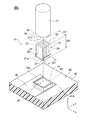
第1実施形態
図1に示すように、本発明の一実施形態に係る圧電駆動装置10は、たとえばカメラなどに取り付けられるレンズ12を保持するレンズ枠(移動体)14を、シャフト16の軸方向(Z軸方向)に沿って移動させるレンズ駆動装置である。レンズ枠14は、シャフト16の軸方向の所定位置に摩擦で係合させて軸方向移動自在に取り付けてある。
First Embodiment As shown in FIG. 1, the
積層型圧電素子20がZ軸方向に伸縮振動することでシャフト16が振動し、その振動により、シャフト16に対してレンズ枠14をZ軸方向の一方または他方に移動させることになる。いずれの方向にどの程度に移動させるかは、積層型圧電素子20に印加される電圧波形の形や印加時間などにより決定される。
When the laminated
圧電駆動装置10は、シャフト16と、積層型圧電素子20と、錘部材30とを有する。シャフト16は、一般的には円柱形状を有し、たとえばカーボン強化プラスチック、ステンレス等の鋼材、アルミニウム、ポリアミドイミドなどの非鉄金属などで構成される。シャフト16は、レンズ枠14に形成してある貫通孔14aに挿通して係合してあり、レンズ枠14をZ軸方向に移動自在に保持している。なお、図面において、X軸、Y軸およびZ軸は、相互に垂直であり、Z軸は、シャフト16の軸方向にも一致する。
The
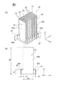
図2に示すように、積層型圧電素子20は、略角柱状(本実施形態では四角柱)の外観形状を有する素子本体21と第1外部電極26と第2外部電極27とを有する。素子本体21は、Z軸方向に相互に反対側に位置する第1端面21aと第2端面21bとを有する。第1端面21aには、第1接着剤60を介して錘部材30が接着してある。また、第2端面21bには、シャフト16の下側端面18が第2接着剤62を介して接着してある。
As shown in FIG. 2, the laminated
素子本体21の内部には、第1端面21aおよび第2端面21bに略垂直な平面(本実施形態ではZ軸に平行な軸を含む平面)を持つ第1および第2内部電極24,25が、圧電体層22を挟んで、Y軸方向に向けて交互に積層してある。第1内部電極24と第2内部電極25とが交互に積層してある圧電体層22の部分が、Z軸方向に伸縮変形する活性部となる。なお、素子本体21の外観形状は、角柱状に限定されず、円柱状、楕円柱状その他の形状であってもよい。
Inside the
図3(A)および図3(B)に示すように、第1内部電極24は、平板状の電極本体24aと、電極本体24aと一体に形成されて、電極本体24aのZ軸方向の下端部からX軸方向に突出するリード部24bと、を有する。電極本体24aのX軸端縁からのリード部24bの突出長さx1は僅かであり、0.3mm以下である。
As shown in FIGS. 3A and 3B, the first
また、リード部24bのZ軸方向の幅z1は、電極本体24aのZ軸方向の高さをz0とした場合に、z1/z0が、好ましくは0.05〜0.2となる関係を満たすように決定される。本実施形態では、リード部24bは、図2に示す素子本体21のX軸方向に向き合っている一側面の下部に形成してある第1外部電極26に接続してある。第1外部電極26のZ軸方向の幅は、リード部24bのZ軸方向の幅と同じであるが、異なっていてもよい。
Further, the width z1 of the
図3(A)および図3(B)に示すように、第2内部電極25は、平板状の電極本体25aと、電極本体25aと一体に形成されて、電極本体25aのZ軸方向の下端部からX軸方向に突出するリード部25bと、を有する。電極本体25aのX軸端縁からリード部25bの突出長さx2は、突出長さx1と同程度である。
As shown in FIGS. 3A and 3B, the second
また、リード部25bのZ軸方向の幅は、リード部25aのZ軸方向の幅z1と同程度である。本実施形態では、リード部25bは、リード部24bとはX軸方向に沿って反対側に突出しており、第1外部電極26の反対側に位置する素子本体21の側面の下部に形成してある第2外部電極27に接続してある。第2外部電極27のZ軸方向の幅は、リード部25bのZ軸方向の幅と同じであるが、異なっていてもよい。
Further, the width of the
本実施形態では、電極本体24a,25aの間に挟まれる圧電層22が活性層となり、圧電層22に電圧が印加されて変位を生じる。電極本体24a,25aのZ軸方向の高さz0は、素子本体21のZ軸方向の高さと略同一であり、電極本体24a,25aのZ軸方向の端部は、それぞれ素子本体21の第1端面21aまたは第2端面21bに露出していてもよい。第1接着剤60および第2接着剤62により覆われるからである。
In the present embodiment, the
ただし、電極本体24a,25aのZ軸方向の端部は、それぞれ素子本体21の第1端面21aまたは第2端面21bから多少引っ込んでいてもよい。あるいは、第1端面21aまたは第2端面21bには、樹脂などで構成してある絶縁保護層が形成してあっても良い。
However, the ends of the
図2に示すように、第1外部電極26および第2外部電極27は、素子本体21のX軸方向に対向する一対の側面のそれぞれのZ軸方向の下端部付近(錘部材30の近く)で、Y軸方向に沿って形成してある。本実施形態では、図1に示すように、錘部材30は、Z軸方向の下側のフレーム40の表面42に形成してある凹部44の内部に第1接着剤60を用いて固定してある。錘部材30の表面は、フレーム40の表面42と略面一となっている。フレーム40は、たとえば図1に示すレンズ保持枠14を囲むケースが取り付けられる固定部材であっても良い。
As shown in FIG. 2, the first
本実施形態では、錘部材30を凹部44の内部に接着する第1接着剤60と同じ接着剤を用いて、錘部材30の表面を素子本体21の第1端面21aに接着して固定してある。
In the present embodiment, the surface of the
図2に示すように、フレーム40の表面には、フレキシブル配線基板(FPC)45が錘部材30(凹部44)を避けるように配置してあり、凹部44のX軸方向に相互に向かい合う開口縁に沿って第1配線45aと第2配線45bとが位置するようになっている。図1に示すように、第1配線45aは、接続部材48aに接続してあり、接続部材48aは、第1外部電極26に接続してある。第2配線45bは、接続部材48bに接続してあり、接続部材48bは、第2外部電極27に接続してある。
As shown in FIG. 2, a flexible wiring board (FPC) 45 is arranged on the surface of the
接続部材48a,48bとしては、特に限定されないが、たとえば導電性ペーストあるいはハンダなどで構成され、第1配線45aと第1外部電極26とを電気的に接続すると共に、第2配線45bと第2外部電極27とを電気的に接続する。
The connecting
図2に示す第1配線45aと第2配線45bとは、フレキシブル配線基板45の内部で絶縁され、それぞれ図1に示す駆動回路50に接続してある。なお、第1配線45aと第2配線45bとは、絶縁性のフレーム40の表面に、それぞれ直接に形成してある回路パターンであっても良い。これらの回路パターンは、絶縁材料で構成してあるフレーム42の表面に、金属ペーストの焼付け法、メッキ法、またはスパッタ法などにより形成することができる。
The
第1内部電極24および第2内部電極25を構成する導電材としては、たとえば、Ag、Pd、Au、Pt等の貴金属およびこれらの合金(Ag−Pdなど)、あるいはCu、Ni等の卑金属およびこれらの合金などが挙げられるが、特に限定されない。
Examples of the conductive material constituting the first
第1外部電極26および第2外部電極27を構成する導電材料も特に限定されず、内部電極を構成する導電材と同様の材料を用いることができる。なお、第1外部電極26および第2外部電極27は、たとえば導電ペーストの焼付けなどにより素子本体21の外面に形成され、その表面には、上記各種金属のメッキ層やスパッタ層が形成してあってもよい。外部電極26,27の厚みは、特に限定されないが、好ましくは0.5〜50μmである。
The conductive material constituting the first
また、圧電体層22の材質は、圧電効果あるいは逆圧電効果を示す材料であれば、特に制限されず、たとえば、PbZrx Ti1−x O3 、BaTiO3 などが挙げられる。また、特性向上等のための成分が含有されていてもよく、その含有量は、所望の特性に応じて適宜決定すればよい。
The material of the
図2に示すように、圧電駆動装置10では、素子本体21のZ軸方向の下端面である第1端面21aに対して対向するように、錘部材30のZ軸方向の上面が配置してある。錘部材30は、全体として直方体形状であるが、その形状は、特に限定されない。
As shown in FIG. 2, in the
錘部材30は、シャフト16に変位を与えるための慣性体として好適に機能するように、タングステン等の比較的比重の大きい金属材料等を含むことが好ましいが特に限定されず、たとえば鉄、鋼材、貴金属、アルミニウムなどの導体で構成してもよい。なお、錘部材30はプラスチック、セラミックなどの絶縁材料で構成してもよい。
The
図1に示す駆動回路50は、積層型圧電素子20に駆動電圧を印加するための回路である。駆動回路50は、フレーム40に取り付けられても良く、フレーム40とは別に設けられても良い。
The
駆動回路50が出力する電圧波形は特に限定されないが、駆動回路50は、たとえばノコギリ波形の電圧波形を出力することにより、積層型圧電素子20の変形量およびこれに伴うシャフト16の変位量を越える移動量を、移動部材としてのレンズ枠14に発生させることができる。
The voltage waveform output by the
本実施形態に係る圧電駆動装置10では、第1端面21aまたは第2端面21bに略垂直な平面をそれぞれ持つ第1内部電極24および第2内部電極25が、圧電層22を挟んで、単一のY軸方向に向けて積層してある。このため、シャフト16などに横から荷重が作用しても、その力は、積層型圧電素子20の素子本体21の内部では、積層してある複数の内部電極24,25を折り曲げる方向に作用し、内部電極24,25の界面を引き剥がす方向には作用しない。したがって、従来とは異なり、積層型圧電素子20の内部での内部電極24,25の積層配列が、素子20の折れ曲がりに抵抗する構造となり、素子20の折れ曲がりやクラックなどを有効に阻止することができる。
In the
また、圧電駆動装置10は、従来の圧電駆動装置とは内部電極の積層方向が異なるために、第1端面21aから第2端面21bに向かう方向の共振に強い構造となり、従来よりも高い周波数での使用が可能となる。そのため、シャフト16へ変位を与える回数を増大させることが可能になり、応答性が向上する。
Further, since the
さらに、第1内部電極24および第2内部電極25が、圧電層22を挟んで、同一方向に沿って繰り返して配置される単純な構造であるために、焼成時などにもクラックが入りにくい構造であると共に、圧電層22の分極も容易である。
Further, since the first
また本実施形態では、図2に示すように、積層型圧電素子20のZ軸方向の高さz01(図3(B)に示す高さz0と略同じ)は、第1内部電極24および第2内部電極25に略垂直な方向に沿った積層型圧電素子20の積層方向厚みy01よりも長いが、特に限定されない。また、本実施形態では、積層型圧電素子20のX軸方向の幅x01は、積層方向厚みy01と同程度であるが、異なっていても良く、特に限定されない。
Further, in the present embodiment, as shown in FIG. 2, the height z01 of the laminated
従来では、第1端面21aと前記第2端面21bとの間の距離を長くするためには、第1端面21aまたは第2端面21bに平行な内部電極の積層数が多くなったり、内部電極が積層されていない圧電層の厚みが厚くなり、圧電層の界面に沿って圧電素子が折れやすくなる。
Conventionally, in order to increase the distance between the
これに対して、本実施形態では、内部電極24,25のZ軸方向の長さを長くすることで、第1端面21aと第2端面21bとの間の距離を長くすることが可能であり、従来に比較して折れにくい構造である。また、内部電極24,25の長手方向の長さを長くすることで、内部電極24,25の面積が大きくなり、内部電極24,25に挟まれる圧電層22の体積を大きくすることが可能になり、圧電素子20のZ軸方向の変位を大きくすることができる。
On the other hand, in the present embodiment, it is possible to increase the distance between the
さらに本実施形態では、第1外部電極26と第2外部電極27とが、第1端面21aの近くに位置する素子本体21の側面に形成してあるため、第1配線45aおよび第2配線45bを、錘部材の近傍のフレーム40の表面に具備させれば良く、配線が容易になる。特に、錘部材30は固定側であるフレーム40に配置されるため、配線が容易である。
Further, in the present embodiment, since the first
また本実施形態では、素子本体21の第1端面21aには、第1接着剤60を介して錘部材30が接着してある。本実施形態では、第1端面21aの近傍に第1外部電極26および第2外部電極27が配置される。そのため、第1接着剤60は、第1外部電極26または第2外部電極27をそれぞれの配線45a,45bに接続するための接続部材48a,48bが第1端面21aに入り込むことを阻止することができる。
Further, in the present embodiment, the
また本実施形態では、第2端面21bには、第2接着剤62を介してシャフト16のZ軸方向の下側端面18が接着してある。この第2接着剤62は、第2端面21bで露出する可能性がある第1内部電極24のZ軸方向端部と第2内部電極25のZ軸方向端部との絶縁を確保することができる。
Further, in the present embodiment, the
本実施形態の素子本体21では、第1内部電極24および第2内部電極25のZ軸方向の各端部は、第1端面21aまたは第2端面21bで露出していてもよい。第1接着剤60は第1端面21aを覆い、第2接着剤62は第2端面21bを覆うことになるので、これらの内部電極24,25が露出する端面を各接着剤60,62が有効に保護することができる。なお、第1端面21aまたは第2端面21bには、予め保護絶縁層が形成してあってもよいことは前述した通りである。
In the element
さらに本実施形態では、第1接着剤60は、錘部材30をフレーム40の凹部44に固定するための部材を兼ねているので、接着剤の無駄がない。また本実施形態では、図1および図2に示すシャフト16の外径は、素子本体21の第2端面21bのサイズ(対角線の長さ)よりも大きいが、同じまたは小さくてもよい。ただし、シャフト16の外径を、素子本体21の第2端面21bのサイズ(外接円の長さ)以上の長さとすることで、下記に示すメリットがある。
Further, in the present embodiment, since the first adhesive 60 also serves as a member for fixing the
すなわち、素子本体21の第2端面21bがシャフト16の下側端面で完全に覆われることから、素子本体21の第2端面21bとシャフト16の下側端面18との接着が均等に成され易く、接着の強度ムラが生じにくいという利点がある。また、素子本体21の変位を効率的にシャフト16に伝達し易いというメリットもある。さらに、素子本体21の第2端面21bがシャフト16の下側端面で完全に覆われることから、シャフト16の外周エッジ部分が内部電極24,25と交差することがなくなる。そのため、圧電層22と内部電極24,25との界面に、シャフト16の外周エッジ部分からの応力が作用することもない。
That is, since the
第2実施形態
図4(A)および図4(B)に示すように、本実施形態に係る圧電駆動装置の積層型圧電素子120は、素子本体121における第1内部電極124と第2内部電極125のパターンが、第1実施形態におけるそれらと相違するのみであり、その他は、第1実施形態と同様な構成を有し、同様な作用効果を奏する。以下、主として相違する部分のみについて詳細に説明し、共通する部分の説明は省略する。また共通する部材には、共通する部材の名称を用い、その詳細な説明は省略する。
2nd Embodiment As shown in FIGS. 4 (A) and 4 (B), the laminated
第1内部電極124は、素子本体121のX軸方向幅と略同一のX軸方向幅を持つ電極本体124aを有し、電極本体124aには、第2外部電極27に対して電気的に絶縁されるように、Z軸方向の下端部でX軸方向の側面には、切欠部124bが形成してある。切欠部124bは、第2外部電極27を完全に避けるように形成してある。切欠部124bとはX軸方向に沿って反対側の電極本体124aの側縁部は、素子本体121の側面から露出して第1外部電極26に接続してある。
The first
これと同様に、第2内部電極125は、素子本体121のX軸方向幅と略同一のX軸方向幅を持つ電極本体125aを有し、電極本体125aには、第1外部電極26に対して電気的に絶縁されるように、Z軸方向の下端部でX軸方向の他の側面には、切欠部125bが形成してある。切欠部125bは、第1外部電極26を完全に避けるように形成してある。切欠部125bとはX軸方向に沿って反対側の電極本体125aの側縁部は、素子本体121の側面から露出して第2外部電極27に接続してある。
Similarly, the second
このようなパターンを有する第1内部電極124と第2内部電極125とを圧電層22を介して交互にY軸方向に積層すれば、第1実施形態の積層型圧電素子20と同様な積層型圧電素子120が得られる。本実施形態では、限られた素子本体121のサイズにおいて、第1実施形態よりも大きな面積の内部電極124,125を交互に配置することが可能になり、活性層の体積が増大し、駆動量を向上させることができる。
If the first
なお、本実施形態では、素子本体121のX軸方向に対向する側面において、外部電極26および27が形成されていない表面で、内部電極124,125の側部が露出する可能性があるため、それらの表面に絶縁保護層が形成してあることが好ましい。
In this embodiment, the side portions of the
第3実施形態
図5(A)および図5(B)に示すように、本実施形態に係る圧電駆動装置の積層型圧電素子220は、素子本体221における第1内部電極224と第2内部電極225のパターンが、第1実施形態におけるそれらと相違するのみであり、その他は、第1実施形態と同様な構成を有し、同様な作用効果を奏する。以下、主として相違する部分のみについて詳細に説明し、共通する部分の説明は省略する。また共通する部材には、共通する部材の名称を用い、その詳細な説明は省略する。
Third Embodiment As shown in FIGS. 5 (A) and 5 (B), the laminated
第1内部電極224は、素子本体221のX軸方向幅よりも狭いX軸方向幅を持つ電極本体224aを有し、電極本体224aには、第2外部電極27に対して電気的に絶縁されるように、X軸方向の一方の側面には、Z軸方向に連続する切欠部224bが形成してある。切欠部224bは、第2外部電極27を完全に避けるように形成してある。切欠部224bとはX軸方向に沿って反対側の電極本体224aの側縁部は、素子本体221の側面から露出して第1外部電極26に接続してある。
The first
これと同様に、第2内部電極225は、素子本体221のX軸方向幅と略同一のX軸方向幅を持つ電極本体225aを有し、電極本体225aには、第1外部電極26に対して電気的に絶縁されるように、Z軸方向の下端部でX軸方向の他の側面には、切欠部225bが形成してある。切欠部225bは、第1外部電極26を完全に避けるように形成してある。切欠部225bとはX軸方向に沿って反対側の電極本体225aの側縁部は、素子本体221の側面から露出して第2外部電極27に接続してある。
Similarly, the second
このようなパターンを有する第1内部電極224と第2内部電極225とを圧電層22を介して交互にY軸方向に積層すれば、第1実施形態の積層型圧電素子20と同様な積層型圧電素子220が得られる。本実施形態では、内部電極224,225のパターンがさらに単純なので、積層型圧電素子220の製造がさらに容易になる。
If the first
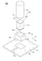
第4実施形態
図6に示すように、本実施形態の圧電駆動装置310は、錘部材330とフレキシブル配線基板45との関係が、第1実施形態〜第3実施形態におけるそれらと相違するのみであり、その他は、第1実施形態〜第3実施形態と同様な構成を有し、同様な作用効果を奏する。以下、主として相違する部分のみについて詳細に説明し、共通する部分の説明は省略する。また共通する部材には、共通する部材の名称を用い、その詳細な説明は省略する。
Fourth Embodiment As shown in FIG. 6, the
本実施形態では、錘部材330のX軸およびY軸を含む平面方向の面積を、第1実施形態の錘部材30に比較して大きくしてあり、錘部材330の表面に、フレキシブル配線基板45の第1配線45aと第2配線45bとを装着してある。また、本実施形態では、図2に示すフレーム40の上に凹部44を設けることなく、錘部材330は、表面42の上に直接に配置する構成でもよい。
In the present embodiment, the area of the
第5実施形態
図7に示すように、本実施形態の圧電駆動装置410は、以下に示す以外が、第1実施形態〜第4実施形態におけるそれらと相違するのみであり、その他は、第1実施形態〜第4実施形態と同様な構成を有し、同様な作用効果を奏する。以下、主として相違する部分のみについて詳細に説明し、共通する部分の説明は省略する。また共通する部材には、共通する部材の名称を用い、その詳細な説明は省略する。
Fifth Embodiment As shown in FIG. 7, the
本実施形態では、積層型圧電素子420の素子本体421の内部では、第1内部電極424が第1端面421aに露出し、第2端面421bには露出しないように配列してある。また、素子本体421の内部では、第2内部電極425が第2端面421bに露出し、第1端面421aには露出しないように配列してある。これらの第1内部電極424および第2内部電極425は、第1端面421aおよび第2端面421bに略垂直な平面を持ち、圧電層22を介してX軸方向に交互に積層してある。
In the present embodiment, inside the
素子本体421の第1端面421aには、その全面を被覆するように、第1外部電極426が形成してあり、第2端面421bには、その全面を被覆するように、第2外部電極427が形成してある。第1外部電極426には、複数の第1内部電極424が接続してあり、第2外部電極427には、複数の第2内部電極425が接続してある。
A first
積層型圧電素子420のZ軸方向の下面に対応する錘部材430の対向面には、第1外部電極426が金属結合される錘側金属面436が形成される。また、錘部材430のZ軸方向の下面も金属面となり、フレーム40の表面42に形成してあるフレーム側回路パターン46(第1配線)に金属結合される。
A weight-
なお、錘部材430はプラスチック、セラミックなどの絶縁材料で構成してもよい。その場合には、積層型圧電素子420のZ軸方向の下面に対応する錘部材430の対向面には、第1外部電極426が金属結合される錘側金属面436を形成する必要があると共に、錘部材430のZ軸方向の下面も金属面とし、それらの間を電気的に接続する必要がある。そこで、絶縁性の錘部材430の表面に、金属膜などで構成される回路パターンを形成すれば良い。
The
また、錘部材430が金属で構成される場合には、金属面となる錘側金属面436および錘取付面438以外の外表面は、絶縁膜で覆っていても良い。
When the
本実施形態において、金属結合させるための方法としては、特に限定されないが、超音波接合、固相拡散接合、摩擦接合などの固相接合技術、レーザー、パルスヒートなどによる溶着接合などが用いられる。 In the present embodiment, the method for metal bonding is not particularly limited, but solid-phase bonding technology such as ultrasonic bonding, solid-phase diffusion bonding, and friction bonding, welding bonding by laser, pulse heat, or the like is used.
フレーム40の表面には、フレーム側回路パターン46と、それに一体化して接続してあるリードパターン46aとが形成してある。図1に示すように、フレーム側回路パターン46のリードパターン46aには、駆動回路50が接続される。リードパターン46aは、図1に示す駆動回路50に接続してある。これらのパターン46,46aは、絶縁材料で構成してあるフレーム42の表面に、金属ペーストの焼付け法、メッキ法、またはスパッタ法などにより形成することができる。
A frame-
本実施形態では、図7に示すように、積層型圧電素子420とシャフト16との接合は、シャフト16のZ軸方向の下側端面18に形成してあるシャフト側金属面と、積層型圧電素子420のZ軸方向の上面に形成してある第2外部電極427との金属結合により行われる。金属結合は、上述した方法により行われる。それぞれの部位の金属結合は、別々に行っても良いが、同時に行っても良い。なお、シャフト16が金属で構成される場合には、シャフト側金属面は、シャフト16のZ軸方向の下側端面18自体であり、金属以外で構成される場合には、シャフト16のZ軸方向の下側端面18に金属面が形成されるように金属膜を形成する。
In the present embodiment, as shown in FIG. 7, the bonding between the laminated
レンズ枠14のZ軸方向移動を邪魔しない位置で、シャフト16のZ軸方向の途中には、シャフト押さえ47がシャフト16に接触している。シャフト押さえ47は、たとえばシャフト16の支持やシャフト16の位置決めなどの機能を有し、レンズ駆動装置には、一般的に取り付けられている。本実施形態では、シャフト押さえ47自体を導電性部材で構成するか、シャフト47自体は絶縁性部材で構成し、シャフト16との接触部に、導電性経路が形成されるように回路パターン、あるいは導電性部材を具備させる。
A
シャフト押さえ47を、導電性部材で構成してある場合には、シャフト押さえ47に、たとえば配線(第2配線)47aを接続する。配線47aは、駆動回路50に接続してある。配線47aの少なくとも一部は、リード線で構成しても良いが、たとえばフレーム40の表面に形成してある回路パターンで構成してあることが好ましい。シャフト押さえ47が絶縁部材で構成してある場合には、配線47aは、シャフト押さえ47の表面に形成してある回路パターンに接続される。シャフト押さえ47の表面に形成してある回路パターンは、シャフト16の表面に電気的に接続される。
When the
シャフト16が導電性部材で構成してあれば、駆動回路50からの一方の電圧は、配線47aを介して、シャフト押さえ47自体またはその回路パターンに伝わり、そこから、シャフト16および下側端面18の金属面を通して、第2外部電極27に伝わる。シャフト16が絶縁部材で構成してある場合では、シャフト16の表面に形成してある回路パターンと、下側端面18の金属面を通して、第2外部電極27に伝わる。駆動回路50からの他方の電圧は、リードパターン46a、フレーム側回路パターン46および錘部材30を通して、第1外部電極26に伝わる。
If the
本実施形態に係る圧電駆動装置410では、積層型圧電素子420には、リード線や金属端子などがハンダなどを介して接続されることは無い。積層型圧電素子420への電力供給は、錘側金属面436と第1外部接続部426との金属結合、およびシャフト16の下側端面18と第2外部接続部427との金属結合により行われる。これらの金属結合が行われる部分は、積層型圧電素子420を駆動させるための逆極性の電圧が印加される部分であると同時に、積層型圧電素子420と錘部材430との連結と、積層型圧電素子420とシャフト16との連結とを兼ねている。
In the
そのため、積層型圧電素子420と錘部材430との強固な連結と、積層型圧電素子420とシャフト16との強固な連結と、積層型圧電素子420への電気的接続のための配線とを同時に確保することができる。したがって、積層型圧電素子420を小型化しても、積層型圧電素子420と錘部材430との連結が容易になると共に、積層型圧電素子420とシャフト16との連結も容易になり、積層型圧電素子420への電力供給のための配線が容易になる。また、これらの自動作業も容易になる。
Therefore, the strong connection between the laminated
さらに、積層型圧電素子420には、リード線や金属端子などの配線部材が錘部材とは別に連結されないため、配線部材に突発的な力が作用することもなく、配線部材との接続部で断線することもない。また、シャフト16の少なくとも一部(全部でも良い)と、錘部材340の少なくとも一部(全部でも良い)が配線を兼ねているので、部品点数の削減にも寄与する。
Further, since the wiring members such as lead wires and metal terminals are not connected to the laminated
さらにまた、金属結合により積層型圧電素子420と錘部材430とが連結されると共に、金属結合により積層型圧電素子420とシャフト16との連結が成されるため、これらの接合強度が向上する。また、これらを接着剤で連結する場合に比較して、接着剤部分での変位吸収が無く、積層型圧電素子420の変位力は、直接に錘部材430およびシャフト16に伝わり、駆動力が向上する(変位のロスが少ない)。
Furthermore, since the laminated
また、本実施形態では、錘部材430を金属で構成することで、錘部材430の密度が高くなり、圧電駆動装置410の小型化に寄与する。また、錘部材430を金属で構成することにより、錘部材430の外表面が、錘側金属面自体を構成することになり、錘部材430とは別に金属面を形成する必要がない。なお、錘部材430を金属以外で構成する場合には、積層型圧電素子と金属結合するための錘側金属面を、たとえば金属膜などの回路パターンなどで形成すればよい。
Further, in the present embodiment, by making the
また、シャフト16には、シャフト押さえ47が接触しており、シャフト16およびシャフト押さえ47を通して、シャフト側金属面に電力が供給可能になっている。たとえばレンズ駆動装置などにおいては、シャフト押さえは、必要な部品であり、部品点数を増大させることなく、シャフト16と下側端面18を介して積層型圧電素子420に電力を供給することができる。
Further, the
さらに本実施形態では、シャフト16が金属である場合には、下側端面18の金属面は、シャフト16自体の外表面を利用して容易に形成することができる。その場合には、シャフト16自体が、電気導通路となる。シャフト16が金属以外の導電性部材である場合にも同様である。ただし、下側端面18に金属面を形成するためには、シャフト16の所定位置に、金属膜などで回路パターンを形成すれば良い。その点は、シャフト16が絶縁体である場合も同様である。
Further, in the present embodiment, when the
また本実施形態では、錘部材430をフレーム40に連結すると同時に、フレーム40に形成してある回路パターン46と錘部材430との電気的接続を行うことができる。これらの接続も金属結合により行うことができる。
Further, in the present embodiment, the
なお、上述した実施形態では、金属結合するための方法として、超音波接合を用いたが、その他の方法を用いても良い。金属結合させるためのその他の方法としては、たとえば拡散接合、摩擦接合、レーザー、パルスヒートなどが例示される。 In the above-described embodiment, ultrasonic bonding is used as the method for metal bonding, but other methods may be used. Other methods for metal bonding include, for example, diffusion welding, friction stir welding, laser, pulse heat and the like.
さらに、本実施形態では、積層型圧電素子20と錘部材30とが金属結合されていると共に、積層型圧電素子20とシャフト16とが金属結合されていれば良く、その他の部分は、金属結合以外でも良い。たとえば、錘部材30とフレーム40とは、金属結合以外の方法、たとえばハンダ接合あるいは接着(導電性接着剤含む)により接合してあっても良い。
Further, in the present embodiment, it is sufficient that the laminated
第6実施形態
図9に示すように、本実施形態の圧電駆動装置510は、以下に示す以外が、第1実施形態〜第5実施形態におけるそれらと相違するのみであり、その他は、第1実施形態〜第5実施形態と同様な構成を有し、同様な作用効果を奏する。以下、主として相違する部分のみについて詳細に説明し、共通する部分の説明は省略する。また共通する部材には、共通する部材の名称を用い、その詳細な説明は省略する。
Sixth Embodiment As shown in FIG. 9, the
本実施形態では、積層型圧電素子520の素子本体521は、第5実施形態の素子本体421と同様に、素子本体521の内部では、第1内部電極424が第1端面521aに露出し、第2端面521bには露出しないように配列してある。また、素子本体521の内部では、第2内部電極425が第2端面521bに露出し、第1端面521aには露出しないように配列してある。これらの第1内部電極424および第2内部電極425は、第1端面521aおよび第2端面521bに略垂直な平面を持ち、圧電層22を介してX軸方向に交互に積層してある。
In the present embodiment, in the
素子本体521の第1端面521aには、その全面を被覆するように、第1外部電極526の第1端面電極部526aが形成してあり、第2端面521bには、その全面を被覆するように、第2外部電極527の第2端面電極部527aが形成してある。第1外部電極526の第1端面電極526aには、複数の第1内部電極424が接続してあり、第2外部電極527の第2端面電極部527aには、複数の第2内部電極425が接続してある。
The first end
第1外部電極526は、第1端面521aに形成してある第1端面電極部526aと、第1端面電極部526aから積層型圧電素子521の一側面に連続して形成してある第1側面電極部526bとを有する。第2外部電極527は、第2端面521bに形成してある第2端面電極部527aと、第2端面電極527aから積層型圧電素子521の他の側面に連続して形成してある第2側面電極部527bとを有する。
The first
本実施形態では、第1側面電極部526bの先端は、素子本体521の第2端面521bの近くに位置するが、第2端面電極部527aには接続されずに絶縁されるように、隙間28aが設けてある。また第2側面電極部527bの先端は、素子本体521の第1端面521aの近くに位置するが、第1端面電極部526aには接続されずに絶縁されるように、隙間28bが設けてある。
In the present embodiment, the tip of the first side
積層型圧電素子520の第1端面521aを錘部材330に接着するための第1接着剤560は、素子520のZ軸方向の下端部周囲で、素子520の側面にまで延びて盛上り部560aが形成される。盛上り部560aは、隙間28bを十分に塞ぐように、第2側面電極部527bの先端部の外周まで覆い、第2側面電極部527bと第1端面電極部526aとの間の絶縁を確保する。
The
積層型圧電素子520の第2端面521bをシャフト16の下端に接着するための第2接着剤562は、素子520のZ軸方向の上端部周囲で、素子520の側面にまで延びて盛上り部562aが形成される。盛上り部562aは、隙間28aを十分に塞ぐように、第1側面電極部526bの先端部の外周まで覆い、第1側面電極部526bと第2端面電極部527aとの間の絶縁を確保する。
The
本実施形態では、第1側面電極部526bに第1配線45aを接続し、第2側面電極部527bに第2配線45bを接続すればよいので、錘部材330の側にのみ、外部回路のための配線45a,45bを具備させれば良くなる。また、第1端面521aは第1端面電極526aで覆われ、第2端面521bは第2端面電極527aで覆われるために、これらの端面521a,521bを有効に保護することができる。
In the present embodiment, the
また、本実施形態では、配線45a,45bと第1側面電極部526bまたは第2側面電極部527bとの接続に用いる接続部材548a,548bは、第1接着剤560の盛上り部560aの上に接触するように形成される。そのため、第2側面電極部527bと第1端面電極部526aとの間の隙間28bに接続部材548bが入り込むことが防止される。
Further, in the present embodiment, the connecting
なお、本実施形態において、シャフト16の下端近くに外部回路への配線45a,45bが配置される場合には、その配線45a,45bと第1側面電極部526bまたは第2側面電極部527bとの接続に用いる接続部材は、第2接着剤562の盛上り部562aの上に接触するように形成され、第1側面電極部526bと第2端面電極部527aとの間の隙間28aに入り込むことが防止される。
In the present embodiment, when the
なお、本発明は、上述した実施形態に限定されるものではなく、本発明の範囲内で種々に改変することができる。 The present invention is not limited to the above-described embodiment, and can be variously modified within the scope of the present invention.
たとえば、上述した実施形態では、圧電駆動装置10,310,410,510として、レンズ12を保持するレンズ枠14をシャフトに沿って移動させる駆動装置を例示したが、移動体としては、レンズ枠以外の部材であっても良い。移動体としては、たとえばスライダーと呼ばれる板バネなどが例示される。
For example, in the above-described embodiment, as the
10,310,410,510… 圧電駆動装置
12… レンズ
14… レンズ枠
14a… 貫通孔
16… シャフト
18… 端面
20,120,220,420,520… 積層型圧電素子
21,121,221,421,521… 素子本体
21a,421a,521a… 第1端面
21b,421b,521b… 第2端面
22… 圧電層
24,124,224,424… 第1内部電極
24a,124a,224a… 電極本体
24b… リード部
124b,224b… 切欠部
25,125,225,425… 第2内部電極
25a,125a,225a… 電極本体
25b… リード部
125b,225b… 切欠部
26,426,526… 第1外部電極
526a… 第1端面電極部
526b… 第1側面電極部
27,427,527… 第2外部電極
527a… 第2端面電極部
527b… 第2側面電極部
28a,28b… 隙間
30,330,430… 錘部材
436… 錘側金属面
438… 錘取付面
40… フレーム
42… 表面
44… 凹部
45… 配線基板
45a… 第1配線
45b… 第2配線
46… フレーム側回路パターン
46a… リードパターン
47… シャフト押さえ
48a,48b,548a,548b… 接続部材
50… 駆動回路
60,560… 第1接着剤
560a… 盛上り部
62,562… 第2接着剤
562a… 盛上り部
10, 310, 410, 510 ...
Claims (5)
前記積層型圧電素子の第1端面に取り付けられる錘部材と、
前記積層型圧電素子の前記第2端面に取り付けられるシャフトと、を有し、
前記積層型圧電素子を駆動することにより、 前記シャフトに対して軸方向に移動自在に係合された移動部材を軸方向に沿って移動させる圧電駆動装置であって、
前記積層型圧電素子の内部では、前記シャフトの軸方向に平行な軸を含む平面をそれぞれ持つ第1内部電極および第2内部電極が、圧電層を挟んで、前記第1内部電極および前記第2内部電極に略垂直な方向に向けて積層してあり、
前記第1端面には、第1接着剤を介して前記錘部材が接着してあり、
前記第1内部電極に接続してある第1外部電極が、前記第1端面に形成してあり、前記第2内部電極に接続してある第2外部電極が、前記第2端面に形成してあり、
前記第1外部電極は、前記第1端面に形成してある第1端面電極部と、前記第1端面電極部から前記積層型圧電素子の一側面に連続して形成してある第1側面電極部とを有し、
前記第2外部電極は、前記第2端面に形成してある第2端面電極部と、前記第2端面電極から前記積層型圧電素子の他の側面に連続して形成してある第2側面電極部とを有し、
前記第2側面電極部の先端部は、前記第1端面電極部の近くに位置し、前記第1接着剤の盛り上げ部により、前記第1端面電極部との絶縁が確保されていることを特徴とする圧電駆動装置。 A laminated piezoelectric element having a first end face and a second end face located on the side opposite to the first end face.
A weight member attached to the first end surface of the laminated piezoelectric element,
It has a shaft attached to the second end surface of the laminated piezoelectric element, and has.
A piezoelectric drive device that moves a moving member movably engaged with the shaft in the axial direction by driving the laminated piezoelectric element.
Inside the laminated piezoelectric element, the first internal electrode and the second internal electrode having a plane including an axis parallel to the axial direction of the shaft sandwich the piezoelectric layer, and the first internal electrode and the second internal electrode are interposed. Ri Thea laminated toward the direction substantially perpendicular to the internal electrodes,
The weight member is adhered to the first end surface via a first adhesive.
The first external electrode connected to the first internal electrode is formed on the first end surface, and the second external electrode connected to the second internal electrode is formed on the second end surface. Yes,
The first external electrode includes a first end surface electrode portion formed on the first end surface and a first side surface electrode formed continuously from the first end surface electrode portion on one side surface of the laminated piezoelectric element. Has a part and
The second external electrode includes a second end surface electrode portion formed on the second end surface and a second side surface electrode formed continuously from the second end surface electrode to another side surface of the laminated piezoelectric element. Has a part and
The tip of the second side surface electrode portion is located near the first end face electrode portion, and the raised portion of the first adhesive ensures insulation from the first end face electrode portion. Piezoelectric drive device.
前記第1側面電極部の先端部は、前記第2端面電極部の近くに位置し、前記第2接着剤の盛り上げ部により、前記第2端面電極部との絶縁が確保されている請求項1または2に記載の圧電駆動装置。 The shaft is adhered to the second end surface via a second adhesive.
Claim 1 in which the tip end portion of the first side surface electrode portion is located near the second end face electrode portion, and insulation from the second end face electrode portion is ensured by the raised portion of the second adhesive. Alternatively, the piezoelectric drive device according to 2.
Priority Applications (3)
| Application Number | Priority Date | Filing Date | Title |
|---|---|---|---|
| JP2016177117A JP6828331B2 (en) | 2016-09-09 | 2016-09-09 | Piezoelectric drive |
| US15/695,485 US10897004B2 (en) | 2016-09-09 | 2017-09-05 | Piezoelectric drive device |
| CN201710805295.3A CN107809185B (en) | 2016-09-09 | 2017-09-08 | piezoelectric driving device |
Applications Claiming Priority (1)
| Application Number | Priority Date | Filing Date | Title |
|---|---|---|---|
| JP2016177117A JP6828331B2 (en) | 2016-09-09 | 2016-09-09 | Piezoelectric drive |
Publications (2)
| Publication Number | Publication Date |
|---|---|
| JP2018042441A JP2018042441A (en) | 2018-03-15 |
| JP6828331B2 true JP6828331B2 (en) | 2021-02-10 |
Family
ID=61560328
Family Applications (1)
| Application Number | Title | Priority Date | Filing Date |
|---|---|---|---|
| JP2016177117A Active JP6828331B2 (en) | 2016-09-09 | 2016-09-09 | Piezoelectric drive |
Country Status (3)
| Country | Link |
|---|---|
| US (1) | US10897004B2 (en) |
| JP (1) | JP6828331B2 (en) |
| CN (1) | CN107809185B (en) |
Families Citing this family (2)
| Publication number | Priority date | Publication date | Assignee | Title |
|---|---|---|---|---|
| CN114793316A (en) * | 2021-01-26 | 2022-07-26 | 北京小米移动软件有限公司 | Sound production module and electronic equipment |
| CN117897889A (en) * | 2021-08-24 | 2024-04-16 | 尼得科株式会社 | Motor |
Family Cites Families (15)
| Publication number | Priority date | Publication date | Assignee | Title |
|---|---|---|---|---|
| JPS59122200A (en) * | 1982-12-28 | 1984-07-14 | Nec Corp | Method for connecting electrically internal electrode of electrostrictive element |
| JPH0217860U (en) * | 1988-07-20 | 1990-02-06 | ||
| JP3147964B2 (en) * | 1992-01-21 | 2001-03-19 | セイコーエプソン株式会社 | Laminated piezoelectric displacement element unit and ink jet recording head |
| DE19909450A1 (en) * | 1999-03-04 | 2000-09-07 | Bosch Gmbh Robert | Piezoelectric actuator |
| JP2004002069A (en) | 2002-05-30 | 2004-01-08 | Tdk Corp | Processes for manufacturing piezoelectric ceramic and piezoelectric element |
| US6919964B2 (en) * | 2002-07-09 | 2005-07-19 | Therma-Wave, Inc. | CD metrology analysis using a finite difference method |
| JP4747795B2 (en) * | 2005-11-16 | 2011-08-17 | Tdk株式会社 | Actuator, slider unit, suspension, hard disk device, and piezoelectric element used in these |
| JP2008199773A (en) | 2007-02-13 | 2008-08-28 | Konica Minolta Opto Inc | Driving apparatus, and manufacturing method of driving apparatus |
| JP2010259193A (en) * | 2009-04-23 | 2010-11-11 | Nikon Corp | Drive device and robot |
| JP5465337B2 (en) * | 2010-10-28 | 2014-04-09 | 京セラ株式会社 | Multilayer piezoelectric element, injection device using the same, and fuel injection system |
| JP5591292B2 (en) * | 2012-09-14 | 2014-09-17 | Tdk株式会社 | Piezoelectric unit |
| JP2014168132A (en) * | 2013-01-31 | 2014-09-11 | Teijin Ltd | Polymer piezoelectric speaker |
| JP5724120B1 (en) * | 2014-02-27 | 2015-05-27 | Tdk株式会社 | Piezoelectric element unit and driving device |
| JP5915703B2 (en) | 2014-02-27 | 2016-05-11 | Tdk株式会社 | Piezoelectric element unit and driving device |
| JP5971286B2 (en) * | 2014-07-29 | 2016-08-17 | Tdk株式会社 | Lens drive device |
-
2016
- 2016-09-09 JP JP2016177117A patent/JP6828331B2/en active Active
-
2017
- 2017-09-05 US US15/695,485 patent/US10897004B2/en active Active
- 2017-09-08 CN CN201710805295.3A patent/CN107809185B/en active Active
Also Published As
| Publication number | Publication date |
|---|---|
| US10897004B2 (en) | 2021-01-19 |
| US20180076380A1 (en) | 2018-03-15 |
| CN107809185A (en) | 2018-03-16 |
| JP2018042441A (en) | 2018-03-15 |
| CN107809185B (en) | 2019-12-10 |
Similar Documents
| Publication | Publication Date | Title |
|---|---|---|
| US10353168B2 (en) | Lens driving device | |
| JP7128628B2 (en) | Laminated piezoelectric ceramic parts and piezoelectric devices | |
| JP2018152541A (en) | Vibrating device | |
| JP2015057838A (en) | Electronic component | |
| JP2007329431A (en) | Piezoelectric exciter | |
| WO2019087922A1 (en) | Vibration device | |
| JP6828331B2 (en) | Piezoelectric drive | |
| JP7088341B2 (en) | Vibration device | |
| WO2006022257A1 (en) | Ceramic electronic component | |
| JP5429140B2 (en) | Piezoelectric actuator | |
| JP6439715B6 (en) | Piezoelectric drive | |
| JP6331475B2 (en) | Piezoelectric device | |
| JP5664203B2 (en) | Electronic components | |
| JP6439714B6 (en) | Piezoelectric drive | |
| US10347816B2 (en) | Piezoelectric driving device | |
| JP7172401B2 (en) | Piezoelectric actuators and piezoelectric drives | |
| JP5971286B2 (en) | Lens drive device | |
| JP7234594B2 (en) | Vibration device and electronic equipment | |
| JP7087942B2 (en) | Vibration devices, electronic devices, and how to drive vibration devices | |
| JP7167653B2 (en) | Vibration device, connection structure, and method for manufacturing vibration device | |
| JP7003415B2 (en) | Vibration device | |
| JP6726508B2 (en) | Piezoelectric actuator | |
| WO2019087923A1 (en) | Vibration device | |
| JP2016180993A (en) | Piezoelectric element unit, lens drive device, and method for manufacturing piezoelectric element unit | |
| JP2018129447A (en) | Vibration device |
Legal Events
| Date | Code | Title | Description |
|---|---|---|---|
| A621 | Written request for application examination |
Free format text: JAPANESE INTERMEDIATE CODE: A621 Effective date: 20190524 |
|
| A131 | Notification of reasons for refusal |
Free format text: JAPANESE INTERMEDIATE CODE: A131 Effective date: 20200401 |
|
| A977 | Report on retrieval |
Free format text: JAPANESE INTERMEDIATE CODE: A971007 Effective date: 20200330 |
|
| A521 | Request for written amendment filed |
Free format text: JAPANESE INTERMEDIATE CODE: A523 Effective date: 20200519 |
|
| A02 | Decision of refusal |
Free format text: JAPANESE INTERMEDIATE CODE: A02 Effective date: 20200714 |
|
| A521 | Request for written amendment filed |
Free format text: JAPANESE INTERMEDIATE CODE: A523 Effective date: 20201006 |
|
| C60 | Trial request (containing other claim documents, opposition documents) |
Free format text: JAPANESE INTERMEDIATE CODE: C60 Effective date: 20201006 |
|
| A911 | Transfer to examiner for re-examination before appeal (zenchi) |
Free format text: JAPANESE INTERMEDIATE CODE: A911 Effective date: 20201021 |
|
| C21 | Notice of transfer of a case for reconsideration by examiners before appeal proceedings |
Free format text: JAPANESE INTERMEDIATE CODE: C21 Effective date: 20201027 |
|
| TRDD | Decision of grant or rejection written | ||
| A01 | Written decision to grant a patent or to grant a registration (utility model) |
Free format text: JAPANESE INTERMEDIATE CODE: A01 Effective date: 20201222 |
|
| A61 | First payment of annual fees (during grant procedure) |
Free format text: JAPANESE INTERMEDIATE CODE: A61 Effective date: 20210104 |
|
| R150 | Certificate of patent or registration of utility model |
Ref document number: 6828331 Country of ref document: JP Free format text: JAPANESE INTERMEDIATE CODE: R150 |