EP2634807A1 - Matrice d'élément électroluminescent semi-conducteur - Google Patents
Matrice d'élément électroluminescent semi-conducteur Download PDFInfo
- Publication number
- EP2634807A1 EP2634807A1 EP13001005.1A EP13001005A EP2634807A1 EP 2634807 A1 EP2634807 A1 EP 2634807A1 EP 13001005 A EP13001005 A EP 13001005A EP 2634807 A1 EP2634807 A1 EP 2634807A1
- Authority
- EP
- European Patent Office
- Prior art keywords
- layer
- semiconductor
- light emitting
- lamination
- semiconductor light
- Prior art date
- Legal status (The legal status is an assumption and is not a legal conclusion. Google has not performed a legal analysis and makes no representation as to the accuracy of the status listed.)
- Withdrawn
Links
Images




Classifications
-
- H—ELECTRICITY
- H10—SEMICONDUCTOR DEVICES; ELECTRIC SOLID-STATE DEVICES NOT OTHERWISE PROVIDED FOR
- H10H—INORGANIC LIGHT-EMITTING SEMICONDUCTOR DEVICES HAVING POTENTIAL BARRIERS
- H10H20/00—Individual inorganic light-emitting semiconductor devices having potential barriers, e.g. light-emitting diodes [LED]
- H10H20/80—Constructional details
- H10H20/84—Coatings, e.g. passivation layers or antireflective coatings
-
- H—ELECTRICITY
- H10—SEMICONDUCTOR DEVICES; ELECTRIC SOLID-STATE DEVICES NOT OTHERWISE PROVIDED FOR
- H10H—INORGANIC LIGHT-EMITTING SEMICONDUCTOR DEVICES HAVING POTENTIAL BARRIERS
- H10H20/00—Individual inorganic light-emitting semiconductor devices having potential barriers, e.g. light-emitting diodes [LED]
- H10H20/01—Manufacture or treatment
- H10H20/011—Manufacture or treatment of bodies, e.g. forming semiconductor layers
- H10H20/018—Bonding of wafers
-
- H—ELECTRICITY
- H10—SEMICONDUCTOR DEVICES; ELECTRIC SOLID-STATE DEVICES NOT OTHERWISE PROVIDED FOR
- H10H—INORGANIC LIGHT-EMITTING SEMICONDUCTOR DEVICES HAVING POTENTIAL BARRIERS
- H10H20/00—Individual inorganic light-emitting semiconductor devices having potential barriers, e.g. light-emitting diodes [LED]
- H10H20/80—Constructional details
- H10H20/85—Packages
- H10H20/851—Wavelength conversion means
- H10H20/8511—Wavelength conversion means characterised by their material, e.g. binder
- H10H20/8512—Wavelength conversion materials
- H10H20/8513—Wavelength conversion materials having two or more wavelength conversion materials
-
- H—ELECTRICITY
- H10—SEMICONDUCTOR DEVICES; ELECTRIC SOLID-STATE DEVICES NOT OTHERWISE PROVIDED FOR
- H10H—INORGANIC LIGHT-EMITTING SEMICONDUCTOR DEVICES HAVING POTENTIAL BARRIERS
- H10H20/00—Individual inorganic light-emitting semiconductor devices having potential barriers, e.g. light-emitting diodes [LED]
- H10H20/80—Constructional details
- H10H20/85—Packages
- H10H20/855—Optical field-shaping means, e.g. lenses
-
- H—ELECTRICITY
- H10—SEMICONDUCTOR DEVICES; ELECTRIC SOLID-STATE DEVICES NOT OTHERWISE PROVIDED FOR
- H10H—INORGANIC LIGHT-EMITTING SEMICONDUCTOR DEVICES HAVING POTENTIAL BARRIERS
- H10H29/00—Integrated devices, or assemblies of multiple devices, comprising at least one light-emitting semiconductor element covered by group H10H20/00
- H10H29/10—Integrated devices comprising at least one light-emitting semiconductor component covered by group H10H20/00
- H10H29/14—Integrated devices comprising at least one light-emitting semiconductor component covered by group H10H20/00 comprising multiple light-emitting semiconductor components
- H10H29/142—Two-dimensional arrangements, e.g. asymmetric LED layout
-
- H—ELECTRICITY
- H10—SEMICONDUCTOR DEVICES; ELECTRIC SOLID-STATE DEVICES NOT OTHERWISE PROVIDED FOR
- H10H—INORGANIC LIGHT-EMITTING SEMICONDUCTOR DEVICES HAVING POTENTIAL BARRIERS
- H10H20/00—Individual inorganic light-emitting semiconductor devices having potential barriers, e.g. light-emitting diodes [LED]
- H10H20/01—Manufacture or treatment
- H10H20/032—Manufacture or treatment of electrodes
-
- H—ELECTRICITY
- H10—SEMICONDUCTOR DEVICES; ELECTRIC SOLID-STATE DEVICES NOT OTHERWISE PROVIDED FOR
- H10H—INORGANIC LIGHT-EMITTING SEMICONDUCTOR DEVICES HAVING POTENTIAL BARRIERS
- H10H20/00—Individual inorganic light-emitting semiconductor devices having potential barriers, e.g. light-emitting diodes [LED]
- H10H20/80—Constructional details
- H10H20/81—Bodies
- H10H20/819—Bodies characterised by their shape, e.g. curved or truncated substrates
Definitions
- This invention relates to a semiconductor light emitting element array and its manufacture.
- LED arrays semiconductor light emitting diode arrays
- LED elements semiconductor light emitting diode elements
- FIG. 5 shows a cross section of a conventional LED array 200.
- An LED array 200 has a structure in which a plurality of gallium nitride series semiconductor light emitting diode elements (LED elements) 201 are disposed on a support substrate 210.
- Respective LED elements are, for example, blue light emitting elements, each having at least a GaN series light emitting part 202 including an n-type GaN layer, an active layer, and a p-type GaN layer, a reflection electrode 203 formed for example of Ag or Al on a rear surface of the light emitting part 202, a wiring layer 208 disposed on a front surface of the light emitting part 202 for diffusing current supplied from a current supply pad into the light emitting part 202, and a melt adhesion layer 206 for connecting the reflection electrode 203 and the support substrate 210.
- blue light emitting elements each having at least a GaN series light emitting part 202 including an n-type GaN layer, an active layer, and a p-type GaN layer, a reflection electrode 203 formed for example of Ag or Al on a rear surface of the light emitting part 202, a wiring layer 208 disposed on a front surface of the light emitting part 202 for diffusing current supplied from a current supply pad into
- a yellow fluorescent material (phosphor) layer 218 formed of a transparent resin including yellow fluorescent (phosphor) powder 219 is coated on the surface of the LED elements 201.
- White lights can be emitted from the LED array 200, by the combination of blue light emitting LED elements 201 and the fluorescent layer 218 containing yellow fluorescent powder 219.
- the LED array 200 a plurality of LED element regions (EL) 201 are separated by an intervening region (isolating groove or street ST).
- the fluorescent layer 218 fills the street ST as well as covering the LED elements 201.
- the amount of fluorescent powder 219 at the street ST becomes higher than that on the LED element 201. Further, there is no blue light emission at the street ST. Therefore, the lights L1 emitting from the street ST become more yellowish (color temperature becomes lower) than the lights L2 emitting from the LED element region EL. Therefore, the conventional LED array 200 may produce uneven color distribution.
- the conventional LED array may produce uneven brightness distribution.
- An object of this invention is to provide an LED array with suppressed uneven brightness distribution and/or uneven color distribution.
- a semiconductor light emitting element array comprising:
- a method of manufacturing a semiconductor light emitting element array comprising steps of:
- Fig. 1A is a schematic plan view of an LED array 100 including a plurality of semiconductor light emitting (LED) elements 101 connected in parallel according to an embodiment of this invention
- Fig. 1B is a schematic cross section of the LED array 100 along line ab.
- the LED array 100 is formed of four LED elements 101 disposed on a support substrate 10 in 2 x 2 matrix configuration, and connected in parallel.
- Each of the LED elements 101 includes a support substrate 10, a GaN series light emitting portion (device structure lamination) 2 including an n-type GaN layer 22, an active layer 23, and a p-type GaN layer 24, a reflection electrode 3 formed for example of Ag or Al and an etching stopper layer 4 formed for example of silicon oxide, both located on a rear (substrate side) surface of the device structure lamination 2, a wiring layer 8 disposed on a front surface of the n-type GaN layer 22 for diffusing current supplied from a current supply pad Pd into the device structure lamination 2, a melt adhesion layer including a first adhesion layer 5 and a second adhesion layer 6 for connecting the reflection electrode 3 and the support substrate 10, a protection layer (insulating layer) 7 covering outer side surfaces of the device structure lamination 2 and melt adhesion layer, and a whole surface electrode 13 formed on the whole rear surface of the support substrate 10.
- a whole surface electrode 13 is formed on a rear surface of the conductive support substrate 10.
- Each LED element 101
- the device structure laminations 2 of the LED elements 101 are formed on the substrate and shaped in four islands as illustrated in Fig. 1A .
- a pair of adjacent LED element portions EL are separated from each other by a street ST.
- four streets ST extend from the cross region CR toward upward/downward and right side/left side ends of the laminations 2.
- the cross region CR can also be regarded as a street because it is between diagonally adjacent islands.
- Bridge portions (connecting portions) BR are formed to bridge adjacent islands of the device structure laminations 2, i.e.
- Adjacent islands of the device structure laminations 2 are mutually connected (mechanically bridged) by a bridge portion BR.
- the bridge portion BR is formed to project upward from the surface of the device structure lamination 2.
- a protection and reflection film 14 is formed on inner side surfaces of the islands of the device structure lamination 2 and the lower surfaces of the bridge portions BR. Under-fill material may be filled in the space surrounded by the protection and reflection film 14, the melt adhesion layer and the support substrate 10, to support the bridge portion BR.
- the bridge portion BR is formed, for example of an undoped GaN layer 21 grown at initial stage of the epitaxial growth (see Fig. 2A ), is electrically insulating and can guide lights.
- the protection and reflection layer 14 has, for example lamination structure of SiO 2 and Ag, and is electrically insulating and optically reflecting.
- Lights are produced in the device structure laminations 2 (especially in the active layer 23) and are emitted in every direction from the element portions EL.
- the reflection electrode 3 and the protection and reflection film 14 reflect incoming lights. Lights can be guided into and propagated in the bridge portions BR having the light guiding property and emitted outward from the streets ST. Thus, uneven brightness distribution between the LED element portions EL and the streets ST is mitigated or suppressed.
- the space defined at the streets ST (space enclosed by the device structure lamination 2, the melt adhesion layer, and the support substrate 10) is capped or covered by the bridge portions BR.
- the bridge portions BR block the fluorescent material from entering into this space.
- the amount of fluorescent powder coated on the device structure lamination 2 and that on the bridge portions BR (above the street ST) become mostly equivalent. Therefore, uneven color distribution between the LED element portion EL and the street ST is mitigated or suppressed. Strictly, the amount of the fluorescent powder on the street ST is less than that on the LED element portions EL, by the thickness of the bridge portions BR.
- Fig. 1C is a schematic plan view of an LED array 100 according to embodiment of this invention, in which semiconductor light emitting (LED) elements 102 are connected in series.
- LED semiconductor light emitting
- LED elements 101 of the LED array 100 are disposed on a support substrate in 2 x 2 matrix configuration, it is possible to connect them in series.
- a p-side electrode 12 which is constituted of the reflection electrode 3 and the first adhesion layer 5.
- the exposed p-side electrode 12 is connected electrically with the n-side wiring layer 8 of the adjacent LED element 101, for example by elongating the wiring layer 8 to reach and overlap the p-side electrode 12.
- An insulating layer 9 is formed on the surface of the support substrate 10 preliminary to formation of the second adhesion layer 6 to avoid short circuit between the adjacent LED elements 101 (see Figs. 3A, 3B ). There is no whole surface electrode on the rear surface of the support substrate 10.
- bridge portions are formed between adjacent LED elements 101 (device structure laminations 2) except the above-mentioned three locations where the p-side electrode 12 is connected with the n-side wiring layer 8.
- the bridge structures lights produced in the device structure lamination (especially the active layer 23) are emitted not only from the LED element portions EL, but also from the streets ST after propagation in the bridge portions BR having the light guiding property.
- the amount of fluorescent powder coated on the device structure lamination 2 and that on the bridge portions BR (above the street ST) become mostly equivalent. Therefore, uneven brightness distribution and uneven color distribution between the LED element portion EL and the street ST are mitigated or suppressed.
- the LED array 100 may have other constructions such as one in which LED elements 101 are aligned in one row, e.g. 1 x 4 matrix configuration, and are electrically connected in parallel or in series. It is also possible to adapt matrix configuration including three rows or more. The number, configuration, and connection style of the LED elements may be changed according to necessity. In any constructions, at least some bridge is provided between adjacent LED elements 101 (device structure laminations 2) to cover street area.
- FIGs. 1A and 1B are cross sections along the line ab shown in Fig. 1A .
- Cross sections illustrate two LED elements 101 among four LED elements, and other two LED elements are simultaneously manufactured.
- a growth substrate for example, a C plane sapphire substrate
- MOCVD organic metal chemical vapor deposition
- the sapphire substrate 1 is loaded in a MOCVD system, and heating (thermal cleaning) is done at 1000 degrees centigrade for 10 minutes in hydrogen atmosphere. Then, a low temperature buffer layer (GaN layer) 20 is grown at about 500 degrees centigrade, by supplying TMG (tri-methyl-gallium) 10.4 micromol/min, NH 3 3.3 SLM (standard liter per minute), for three minutes.
- the growth substrate 1 is a single crystal substrate having lattice constant capable of epitaxially growing a GaN layer, and is selected from the materials transparent for the light at the wavelength of 362 nm, which is the absorption edge of the GaN, for enabling removal of the substrate by laser lift-off. Spinel, SiC, ZnO etc. may also be used as well as sapphire.
- the substrate 1 is heated to 1000 degrees centigrade and maintained thereat for 30 seconds to crystallize the low temperature buffer layer 20.
- an underlying GaN layer (undoped GaN layer) 21 is grown to a thickness of about 5 micrometers by supplying TMG 45 micromol/min, NH 3 4.4 SLM for 100 minutes.
- the undoped GaN layer is grown to a thickness in a range of 1-3 micrometers.
- bridge structure is made from the undoped GaN layer 21, and the undoped GaN layer is grown to a thickness of bout 5 micrometers for securing the mechanical strength of the bridge structure BR (see Figs/ 1A and 1B ).
- the maximum thickness of the undoped GaN layer is preferably selected to be about 10 micrometers.
- the preferable thickness of the undoped GaN layer 21 is in a range of 4-10 micrometrs.
- a Si-doped n-type GaN layer 22 is grown to a thickness of about 5 micrometers by supplying TMG 45 micromol/min, NH 3 4.4 SLM, and SiH 4 2.7x10 -9 micromol/min, for 100 minutes.
- an active layer 23, more specifically multi-quantum-well (MQW) structure is grown at 700 degrees centigrade.
- an InGaN/GaN lamination is set as one period, and growth of 5 periods is performed.
- an InGaN well layer of a thickness of about 2.2 nm is grown by supplying TMG 3.6 micromol/min, TMI (tri-methyl-indium) 10 micromol/min, and NH 3 4.4 SLM, for 33 seconds
- a GaN barrier layer of a thickness of about 15 nm is grown by supplying TMG 3.6 micromol/min, and NH 3 4.4 SLM, for 320 seconds.
- a p-type layer 24 more specifically combination of a Mg-doped p-type AlGaN layer (clad layer) and a Mg-doped p-type GaN layer (contact layer), is grown.
- the temperature is raised to 870 degrees centigrade, a Mg-doped p-type AlGaN layer (clad layer) is grown to a thickness of about 40 nm by supplying TMG 8.1 micromol/min, TMA (tri-methyl-aluminium) 7.5 micromol/min, NH 3 4.4 SLM, and Cp 2 Mg (bis-cyclopentadienyl Mg) 2.9x10 -7 micromol/min for 5 minutes.
- a Mg-doped p-type GaN layer (contact layer) is grown to a thickness of about 150 nm by supplying TMG 18 micromol/min, NH 3 4.4 SLM, and Cp 2 Mg 2.9x10 -7 micromol/min for 7 minutes.
- an Ag layer of a thickness of 200 nm is formed on the surface of the device structure lamination 2 (p-type GaN layer 24) by electron beam evaporation, and is patterned by photolithography and etching, to form a reflection electrode 3.
- the reflection electrode may also be patterned by well-known lift-off.
- the reflection electrode 3 may also be formed of Pt, Pd, Ni, Ti, Al, and alloys thereof, as well as Ag.
- an etching stopper layer 4 formed of SiO 2 preferably of a same thickness as the reflection electrode 3 is formed on the device structure lamination 2 (p-type GaN layer 24) surrounding the reflection electrode 3, by sputtering.
- the etching stopper layer 4 serves as an etch stopper in the etching step as described later referring to Figs. 5O and 5P.
- a first adhesion layer 5 made of an Au film of 200 nm thick is formed on a region including the reflection electrode 3 and the etching stopper layer 4.
- the first adhesion layer 5 may be formed after a diffusion preventing layer, an insulating layer, etc. are formed on the area including the reflection electrode 3 and the etching stopper layer 4.
- a diffusion preventing layer, an insulating layer etc. for example, a diffusion preventing layer made of a TiW film of 300 nm thick is formed by sputtering.
- the diffusion preventing film serves to prevent diffusion of a material used as the reflection electrode 3.
- the reflection electrode When Ag is included in the reflection electrode, those materials as Ti, W, Pt, Pd, Mo, Ru, Ir, Au, and alloys thereof can be used. On the diffusion preventing layer, it is preferable to form an insulating layer made of SiO 2 by CVD, etc.
- the device structure lamination 2 is divided by etching, forming isolating grooves.
- the initially grown undoped GaN layer 21 is not etched and left.
- a resist pattern PR1 is formed on the device structure lamination 2, covering the reflection electrode 3, the etching stopper layer 4, and the first adhesion layer 5, by using the conventional photolithography.
- Fig. 2F using the resist pattern PR1 as an etching mask, exposed device structure lamination 2 is etched by dry etching until the surface of the undoped GaN layer 21 is exposed. The resist pattern PR1 is then removed. Remaining undoped GaN layer 21 will form bridge portions BR (see Figs. 1A and 1B ) in the later process.
- a protection reflection layer 14 is formed on the etched groove (isolating groove) of the device structure lamination 2.
- a resist pattern exposing only the isolating grooves is formed by photolithography.
- a SiO 2 film 14 is deposited by sputtering to a thickness of about 300 nm in the isolating grooves to form an insulating and protecting film on the isolating grooves.
- an Ag film is deposited on the siO 2 film 14 by sputtering to a thickness of about 150 nm to form a reflection film.
- Ti (150nm) / SiO2 (300 nm) lamination is deposited by sputtering. Unnecessary portions are removed by lift-off to leave the protection reflection film 14 only in the isolating grooves.
- underfill material may be filled in the isolating grooves.
- a support substrate 10 for example a silicon substrate, is prepared.
- a second adhesion layer 6 made of AuSn (Sn:20 wt%) having a thickness of 1 micometer is formed on the support substrate 10 by resistance heating.
- the support substrate 10 is preferably formed of a material having a thermal expansion coefficient near those of sapphire (7.5 x 10 -6 / K) and GaN (5.6 x 10 -6 / K), and a high thermal conductivity. For example, Si, AlN, Mo, W, CuW etc. may be used.
- the first adhesion layer 5 and the second adhesion layer 6 may be formed of metals including Au-Sn, Au-In, Pd-In, Cu-In, Cu-Sn, Ag-Sn, Ag-In, Ni-Sn, etc. capable of melt adhesion, or metals including Au capable of diffusion adhesion.
- the second adhesion layer 6 may be formed by utilizing lift-off, as depicted in Figs. 2H and 2I .
- a photoresist for example photoresist AZ5200 available from Clariant Co.
- prebaking on a hot plate set under 90 degrees centigrade, for about 90 seconds in air.
- the photoresist layer is pattern-exposed with first exposure amount of 17 mJ using ultraviolet (UV) lights.
- UV ultraviolet
- photoresist film is immersed in developing liquid for 130 seconds to perform developing, to obtain desired photoresist pattern PR2 (in areas except the area of the second adhesion layer 6).
- the photoresist pattern PR2 thus formed has peripheral portion with reverse taper shape (upwardly broadening shape). The resist material and the conditions of photolithography can be changed appropriately.
- a metal lamination 6 comprising Ti (150 nm) / Ni (50 nm) /Au (100 nm) /Pt (200 nm) /AuSn (1000 nm, Sn: 20wt%) is deposited on the support substrate by resistance heating, and subjected to lift-off to form a second adhesion layer 6 having a tapered peripheral shape with respect to the support substrate 10 (upwardly narrowing cross section), as depicted in Fig. 2I .
- the shape of the second adhesion layer 6 is not limited to the depicted forward taper shape, provided that the angle formed by the surface (upper surface) to be adhered with the first adhesion layer 5 and the side surface is an obtuse angle (angle > 90 degrees), and the angle of the side surface with respect to the support substrate is always 0 degree ⁇ angle ⁇ 90 degrees.
- the second adhesion layer 6 may also be formed by dry etching or wet etching, as well as lift-off.
- a metal lamination 6 of Ti (150 nm) / Ni (50 nm) /Au (100 nm) /Pt (200 nm) /AuSn (1000 nm, Sn: 20wt%) is deposited on a whole surface of a thermally oxidized support substrate 10 by resistance heating, a resist pattern of desired pattern (covering the areas to become the second adhesion layer 6) is formed on the metal lamination 6, and the exposed metal lamination 6 is removed by etching to the interface with the substrate (patterning the metal lamination), to form the second adhesion layer as depicted in Fig.
- Dry etching may be done with etchant of Ar, Cl 2 , and CF 4 , and wet etching may be done with etchants, for example aquous solution of iodine and ammonium iodide for Au.
- the first adhesion layer 5 and the second adhesion layer 6 are brought into pressed contact with a pressure of 3 MPa, are heated to 300 degrees centigrade, maintained for 10 minutes, and then cooled down to achieve melt adhesion.
- An adhesion layer is formed by this melt adhesion.
- element portions EL and streets ST are defined (see Fig. 1B ).
- UV excimer laser lights are irradiated from the rear surface side of the sapphire substrate 1, to heat and decompose the buffer layer 20.
- the sapphire substrate 1 is separated (removed) from the device structure lamination 2 by laser lift-off, as depicted in Fig. 2L .
- KrF excimer laser emitting lights of wavelength 248 nm may be used as the laser.
- Laser power may be about 800 mJ/cm 2 .
- the GaN layer on the sapphire substrate 1 is decomposed into metal Ga and nitrogen. The new surface exposed after laser lift-off will be the undoped GaN layer 21. Removal of the growth substrate 1 may also be done by other methods than laser lift-off, such as etching.
- the initial growth layer (undoped GaN layer) 21 in the element regions EL will be completely removed by etching, to expose the n-type GaN layer 22.
- the initially grown layer (undoped GaN layer) 21 in the street regions ST is protected from etching, to be left and constitute bridge portions BR.
- the undoped GaN layer 21 in the exposed areas is removed by etching by its entire thickness (about 5 micrometers in this embodiment) using the photoresist pattern PR as an etching mask, to expose the underlying n-type GaN layers 22 as depicted in Fig. 2N . Thereafter, the photoresist pattern PR3 is removed.
- bridge portions BR formed of initially grown layer (undoped GaN layer 21) can be formed in the street regions.
- the bridge portions BR are formed of the undoped GaN layer, and have light guiding and electrically isolating (insulating) properties.
- a pair of LED elements 2 connected by a bridge BR can be electrically isolated and optically coupled.
- the surface of the n-type GaN layer 22 exposed by etching is capable of forming electrical contact with an electrode (wiring) 8.
- the exposed surface of the n-type semiconductor layer 22 may be provided with micro cone structures, for example by alkaline treatment, to improve the light output efficiency.
- a photoresist pattern PR4 is formed on the device structure lamination 2 to expose peripheries of the device structure lamination 2. Then, the device structure lamination 2 exposed outside the photoresist pattern PR4 is etched by dry etching using chlorine gas until the etching stopper layer 4 is exposed. As depicted in Fig. 2P , the outer side surface of the device structure lamination 2 takes a tapered shape. When the support substrate 10 assumes a lower position, the outer side surface of the device structure lamination 2 formed on the upper surface of the support substrate 10 has an upwardly decreasing cross section (forward taper with respect to the support substrate 10).
- Part of the etching stopper layer 4 and the first adhesion layer 5 may be etched to realize a configuration in which the angle formed by an upper surface and a side surface of the adhesion layer including the first and second adhesion layers (including the reflection electrode 3 and remaining part of the etching stopper layer 4) is larger than 90 degrees, and the side surface does not include any part where the side surface of the adhesion layer forms an angle larger than 90 degrees with the upper surface of the support substrate.
- the side surface of the adhesion layer forms forward taper with respect to the upper surface of the support substrate.
- a protection film (insulating film) 7 made of SiO 2 is formed on the whole upper surface of the device formed by the above-mentioned process by CVD. Selected portions of the protection film 7 formed on the device structure lamination 2 are etched using buffered fluoric acid to expose portions of the surface of the device structure lamination 2 (surface of the n-type GaN layer 22) and the bridge portions BR.
- a Ti layer of a thickness 1 nm, an Al layer of a thickness 200 nm, a Ti layer of a thickness 100 nm, and an Au layer of a thickness 2 micrometers are sequentially deposited on the structure by electron beam deposition, and patterned by lift-off, to form wiring electrodes 8 having a width of about 10 nm on the surface of the n-type GaN layer 22.
- the width of the wiring electrode is preferably in a range of 3-10 micrometers.
- the plan shape of the wiring electrode 8 is not limited to the one depicted in Fig. 1A , and may take any shape such as comb tooth shapes, radial shapes, concentric shapes, etc.
- the support substrate 10 may be divided by laser scribing or dicing.
- fluorescent material is coated on the surface of the LED array 100, to form the fluorescent layer 108 as depicted in Fig. 1B .
- the fluorescent layer 108 is formed, for example of fluorescent material containing resin in which fluorescent powder is mixed in binder resin.
- the fluorescent material may include single or plural species of red fluorescent material (CaAlSiN 3 :EU 2+ , (Ca, Sr)AlSiN 3 :EU 2+ , Ca 2 Si 5 N 8 :Eu 2+ , (Ca, Sr) 2 Si 5 N 8 :EU 2+ , KSiF 6 :Mn 4+ , etc.), yellow fluorescent material (Y 3 Al 5 O 12 :Ce 3+ , (Sr, Ba) 2 SiO 4 :Eu 2+ , Ca x (Si, Al) 12 (O, N) 16 :Eu 2+ , etc.), green fluorescent material (Lu 3 Al 5 O 12 :Ce 3+ , Y 3 (Ga, Al) 5 O 12 :Ce 3+ , Ca 3 SC 2 Si 3 O 12 :Ce 3+ , CaSc 2 O 4 :E
- the resin material may be silicone resin, epoxy resin, etc.
- a fluorescent plate formed by sintering fluorescent material without using resin may also be used.
- the thickness of the fluorescent material layer 108 is of the order of 20-300 micrometers. An optimum thickness can be selected based on efficiency and grain size of the fluorescent material, desired chromaticity, etc.
- fluorescent material is mixed in silicone resin.
- the mixed material is coated on the surface of the device (LED elements 101 and bridges BR) by potting, and cured at about 150 degrees centigrade for 4 hours.
- a fluorescent material layer 108 of a thickness 200-300 micometers will be formed on the element. Species of the fluorescent material, mixing ratio with resin, and amount of coating are appropriately adjusted based on desired color temperature.
- the fluorescent material layer will take a shape of approximately semi-sphere due to surface tension, although the curvature changes depending on the shape of the device.
- Figs. 3A and 3B are schematic cross sections along lines cd and ef in Fig. 1C , in case of connecting LED elements 101 of the LED array 100 in series.
- a support substrate 10 made of silicon is thermally oxidized to form an insulating film (thermally oxidized silicon oxide film) 9 on the surface of the support substrate 10.
- the thickness of the insulating film is enough if sufficient insulation is secured.
- a Ti layer of a thickness 1 nm, an Al layer of a thickness 200 nm, a Ti layer of a thickness 100 nm, and an Au layer of a thickness 2 micrometers are sequentially deposited on the structure by electron beam deposition, and patterned by lift-off, thereby connecting the n-type GaN layer 22 of one element and the electrode 12 (p-side electrode) of the adjacent element.
- the element structure (device structure lamination 2, the adhesion layer including the first and second adhesion layers) on the support substrate 10 may be shaped to have only one or two sides on which the wiring layer 8 is formed, have outwardly spreading slope.
- Fig. 4A and Fig. 4B are diagrams showing structures of automotive lightings (headlamps) 50 equipped with the LED arrays 100 according to the embodiment of the present invention.
- Fig. 4A shows an example of a projection optical system 51.
- the projection lens 105 is designed to make optical source image 106 of the LED array 100 on a virtual vertical screen (projection surface) 107 which faces a front of a vehicle.
- a projection optical system 51 can be equipped with a multireflector (reflection surfaces) 103 and a projection lens 105, to share the projection lens 105 with a plurality of LED arrays 100.
- the headlamp 50 shown in Fig. 4B includes light sources formed of at least two LED arrays each having an LED array 101 and a fluorescent material layer 108 covering the LED array, and a projection optical system 51 including reflection surfaces 103 which are multireflectors divided into a plurality of small reflection regions, a shade 104 and a projector lens 105.
- the reflection surface 103 is a spheroidal reflection surface whose first focal point is set near the light source and second focal point is set neat the upper edge of the shade 104, and it is positioned to cover the side and the front of the light source so that lights from the light source irradiate the reflection surface 103.
- the reflection surface 103 projects the light source images 106 of the plurality of the LED arrays 100 of the light source to the front of a vehicle and is designed to project the light source images 106 of the LED arrays 100 on the virtual vertical screen (projection surface) 107 which faces the front of the vehicle.
- the shade 104 is a shading part for shading a portion of reflected light from the reflection surface 103 to form a cutoff line suitable for a headlamp.
- the shade 104 is disposed between the projection lens 105 and the light source 102, placing its upper edge near the focal point of the projection lens 105.
- the projection lens 105 is positioned on the front of the vehicle and irradiates the reflected light from the reflection surface 103 onto the projection surface 107.
- At least one bridge is provided between adjacent light emitting elements, wherein the adjacent light emitting elements are not limited to those aligned side by side, but may be any other pair in which some space separate the pair, for example diagonally adjacent pair.
- the bridge can prevent filling the space or groove (street) between the pair of light emitting elements with fluorescent material.
- the amount of the fluorescent material in the street can be set equivalent or lower than the amount of the fluorescent material on the element area (light emitting surface).
- color temperature can be uniformalized between the street and the element area, to suppress uneven color distribution.
- the bridge can guide light, and hence lights emitted in the element area can propagate in the bridge, and can be taken out from the street. Thus, uneven brightness distribution can be suppressed between the street and the element portion.
Landscapes
- Led Devices (AREA)
- Non-Portable Lighting Devices Or Systems Thereof (AREA)
Abstract
Description
- This invention relates to a semiconductor light emitting element array and its manufacture.
-
-
Figs. 1A and 1B are a schematic plan view and a schematic cross section of a parallel connection type semiconductor lightemitting element array 100 according to embodiment of this invention, andFig. 1C is a schematic plan view of a serial connection type semiconductor lightemitting element array 100 according to embodiment of this invention. -
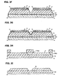
Figs. 2A-2R are schematic cross sections illustrating manufacture processes of the parallel connection type semiconductor lightemitting element array 100 according to the embodiment of this invention. -
Figs. 3A and 3B are schematic cross sections depicting manufacture processes of the serial connection type semiconductor lightemitting element array 100 according to the embodiment of this invention. -
Figs 4A and 4B are diagrams illustrating the structure of an automobile lighting device (head lamp) embodying the semiconductor lightemitting element array 100 according to the embodiment of this invention. -
Fig. 5 is a schematic cross section of a conventional semiconductor lightemitting element array 200. - Semiconductor light emitting devices are used for illumination, for example as automobile head lamps. For example, semiconductor light emitting diode arrays (LED arrays) including a plurality of semiconductor light emitting diode elements (LED elements) connected in series, or in parallel, or in parallel and in series are used as the semiconductor light emitting devices (for example, see Japanese Laid-open Patent Publication No.
2001-156331 -
Fig. 5 shows a cross section of aconventional LED array 200. AnLED array 200 has a structure in which a plurality of gallium nitride series semiconductor light emitting diode elements (LED elements) 201 are disposed on asupport substrate 210. Here, the term "gallium nitride series" means group III-V compound semiconductor AlxGayInzN (0<or=x<or=1, 0<or=y<or=1, 0<or=z<or=1, x + y + z = 1). - Respective LED elements are, for example, blue light emitting elements, each having at least a GaN series
light emitting part 202 including an n-type GaN layer, an active layer, and a p-type GaN layer, areflection electrode 203 formed for example of Ag or Al on a rear surface of thelight emitting part 202, awiring layer 208 disposed on a front surface of thelight emitting part 202 for diffusing current supplied from a current supply pad into thelight emitting part 202, and amelt adhesion layer 206 for connecting thereflection electrode 203 and thesupport substrate 210. - A yellow fluorescent material (phosphor)
layer 218 formed of a transparent resin including yellow fluorescent (phosphor)powder 219 is coated on the surface of theLED elements 201. White lights can be emitted from theLED array 200, by the combination of blue light emittingLED elements 201 and thefluorescent layer 218 containing yellowfluorescent powder 219. - In the
LED array 200, a plurality of LED element regions (EL) 201 are separated by an intervening region (isolating groove or street ST). Thefluorescent layer 218 fills the street ST as well as covering theLED elements 201. The amount offluorescent powder 219 at the street ST becomes higher than that on theLED element 201. Further, there is no blue light emission at the street ST. Therefore, the lights L1 emitting from the street ST become more yellowish (color temperature becomes lower) than the lights L2 emitting from the LED element region EL. Therefore, theconventional LED array 200 may produce uneven color distribution. - Also, lights emitting from the street ST are low since there is no light emitting element. Therefore, the conventional LED array may produce uneven brightness distribution.
- An object of this invention is to provide an LED array with suppressed uneven brightness distribution and/or uneven color distribution.
- According to one aspect of this invention, there is provided a semiconductor light emitting element array comprising:
- a support substrate;
- a plurality of semiconductor light emitting elements disposed on said support substrate, a pair of adjacent semiconductor light emitting elements being separated by street, each of the semiconductor light emitting elements including;
- a first electrode formed on the support substrate,
- a semiconductor lamination formed on the first electrode and including a stack of a first semiconductor layer having a first conductivity type, an active layer formed on the first semiconductor layer, and a second semiconductor layer formed on the active layer, and having a second conductivity type different from the first conductivity type, and
- a second electrode selectively formed on the second semiconductor layer of the semiconductor lamination; and
- connection member having electrical insulating property and optically propagating property, disposed to cover at least part of the street between a pair of adjacent semiconductor laminations.
- According to another aspect of this invention, there is provided a method of manufacturing a semiconductor light emitting element array comprising steps of:
- (a) growing on a growth substrate an initial growth layer having electrical insulating property and optical propagating property;
- (b) growing semiconductor lamination including a first semiconductor layer of a first conductivity type on the initial growth layer, an active layer on the first semiconductor layer, and a second semiconductor layer of a second conductivity type different from the first conductivity type on the active layer;
- (c) selectively forming a first electrode on a surface of the second semiconductor layer, forming a first adhesion layer covering the first electrode, defining a first region of the semiconductor lamination covered by the first adhesion layer and a second region of the semiconductor lamination where the second semiconductor layer is exposed;
- (d) removing the second region of the semiconductor lamination to expose the initial growth layer, and leave the first region of the semiconductor lamination;
- (e) forming a second adhesion layer selectively on a support substrate;
- (f) adhering the growth substrate and the support substrate in such a manner that the first adhesion layer and the second adhesion layer are brought into contact each other, melt- adhering the first and second adhesion layers, to form a joined structure including the semiconductor lamination and the support substrate;
- (g) removing the growth substrate from the joined structure to expose the initial growth layer;
- (h) removing the exposed initial growth layer in area corresponding to the first region of the semiconductor lamination to expose the first semiconductor layer and leave the initial growth layer in area corresponding to the second region of the semiconductor lamination;
- (i) selectively forming a second electrode on the exposed first semiconductor layer.
- The object and advantages of the invention will be realized and attained by means of the elements and combinations particularly pointed out in the claims.
- It is to be understood that both the foregoing general description and the following detailed description are exemplary and are not restrictive of the invention, as claimed.
-
Fig. 1A is a schematic plan view of anLED array 100 including a plurality of semiconductor light emitting (LED)elements 101 connected in parallel according to an embodiment of this invention, andFig. 1B is a schematic cross section of theLED array 100 along line ab. TheLED array 100 is formed of fourLED elements 101 disposed on asupport substrate 10 in 2 x 2 matrix configuration, and connected in parallel. - Each of the
LED elements 101 includes asupport substrate 10, a GaN series light emitting portion (device structure lamination) 2 including an n-type GaN layer 22, anactive layer 23, and a p-type GaN layer 24, areflection electrode 3 formed for example of Ag or Al and anetching stopper layer 4 formed for example of silicon oxide, both located on a rear (substrate side) surface of thedevice structure lamination 2, awiring layer 8 disposed on a front surface of the n-type GaN layer 22 for diffusing current supplied from a current supply pad Pd into thedevice structure lamination 2, a melt adhesion layer including afirst adhesion layer 5 and asecond adhesion layer 6 for connecting thereflection electrode 3 and thesupport substrate 10, a protection layer (insulating layer) 7 covering outer side surfaces of thedevice structure lamination 2 and melt adhesion layer, and awhole surface electrode 13 formed on the whole rear surface of thesupport substrate 10. Awhole surface electrode 13 is formed on a rear surface of theconductive support substrate 10. EachLED element 101 is, for example a blue light emitting element. - The
device structure laminations 2 of theLED elements 101 are formed on the substrate and shaped in four islands as illustrated inFig. 1A . As depicted inFig. 1B , a pair of adjacent LED element portions EL are separated from each other by a street ST. When a central area among the four islands is called a cross region CR, four streets ST extend from the cross region CR toward upward/downward and right side/left side ends of thelaminations 2. The cross region CR can also be regarded as a street because it is between diagonally adjacent islands. Bridge portions (connecting portions) BR are formed to bridge adjacent islands of thedevice structure laminations 2, i.e. to cover the space defined at the streets ST (space surrounded by thedevice structure laminations 2, the melt adhesion layers and the support substrate 10) including the cross region CR. Adjacent islands of the device structure laminations 2 (adjacent LED elements 101) are mutually connected (mechanically bridged) by a bridge portion BR. The bridge portion BR is formed to project upward from the surface of thedevice structure lamination 2. - A protection and
reflection film 14 is formed on inner side surfaces of the islands of thedevice structure lamination 2 and the lower surfaces of the bridge portions BR. Under-fill material may be filled in the space surrounded by the protection andreflection film 14, the melt adhesion layer and thesupport substrate 10, to support the bridge portion BR. - The bridge portion BR is formed, for example of an
undoped GaN layer 21 grown at initial stage of the epitaxial growth (seeFig. 2A ), is electrically insulating and can guide lights. The protection andreflection layer 14 has, for example lamination structure of SiO2 and Ag, and is electrically insulating and optically reflecting. - A
fluorescent layer 108 formed of transparent resin and fluorescent powder, for example yellow fluorescence powder, is coated on the surfaces of the LED elements 101 (device structure laminations 2) and bridge portions BR. - Lights are produced in the device structure laminations 2 (especially in the active layer 23) and are emitted in every direction from the element portions EL. The
reflection electrode 3 and the protection andreflection film 14 reflect incoming lights. Lights can be guided into and propagated in the bridge portions BR having the light guiding property and emitted outward from the streets ST. Thus, uneven brightness distribution between the LED element portions EL and the streets ST is mitigated or suppressed. - The space defined at the streets ST (space enclosed by the
device structure lamination 2, the melt adhesion layer, and the support substrate 10) is capped or covered by the bridge portions BR. When thefluorescent layer 108 is coated, the bridge portions BR block the fluorescent material from entering into this space. The amount of fluorescent powder coated on thedevice structure lamination 2 and that on the bridge portions BR (above the street ST) become mostly equivalent. Therefore, uneven color distribution between the LED element portion EL and the street ST is mitigated or suppressed. Strictly, the amount of the fluorescent powder on the street ST is less than that on the LED element portions EL, by the thickness of the bridge portions BR. -
Fig. 1C is a schematic plan view of anLED array 100 according to embodiment of this invention, in which semiconductor light emitting (LED) elements 102 are connected in series. - In the embodiment in which four nitride semiconductor light emitting elements (LED elements) 101 of the
LED array 100 are disposed on a support substrate in 2 x 2 matrix configuration, it is possible to connect them in series. - In this case, parts of the
device structure laminations 2 near the end area of three streets ST (right, left, and downward streets inFig. 1C ) are removed to expose a p-side electrode 12 which is constituted of thereflection electrode 3 and thefirst adhesion layer 5. The exposed p-side electrode 12 is connected electrically with the n-side wiring layer 8 of theadjacent LED element 101, for example by elongating thewiring layer 8 to reach and overlap the p-side electrode 12. An insulatinglayer 9 is formed on the surface of thesupport substrate 10 preliminary to formation of thesecond adhesion layer 6 to avoid short circuit between the adjacent LED elements 101 (seeFigs. 3A, 3B ). There is no whole surface electrode on the rear surface of thesupport substrate 10. - In the
LED array 100 of the serial connection, bridge portions are formed between adjacent LED elements 101 (device structure laminations 2) except the above-mentioned three locations where the p-side electrode 12 is connected with the n-side wiring layer 8. By the bridge structures, lights produced in the device structure lamination (especially the active layer 23) are emitted not only from the LED element portions EL, but also from the streets ST after propagation in the bridge portions BR having the light guiding property. The amount of fluorescent powder coated on thedevice structure lamination 2 and that on the bridge portions BR (above the street ST) become mostly equivalent. Therefore, uneven brightness distribution and uneven color distribution between the LED element portion EL and the street ST are mitigated or suppressed. - The
LED array 100 may have other constructions such as one in which LEDelements 101 are aligned in one row, e.g. 1 x 4 matrix configuration, and are electrically connected in parallel or in series. It is also possible to adapt matrix configuration including three rows or more. The number, configuration, and connection style of the LED elements may be changed according to necessity. In any constructions, at least some bridge is provided between adjacent LED elements 101 (device structure laminations 2) to cover street area. - A method of manufacturing the
LED array 100 of parallel connection depicted inFigs. 1A and 1B will be described hereinafter referring toFigs. 2A-2R , which are cross sections along the line ab shown inFig. 1A . Cross sections illustrate twoLED elements 101 among four LED elements, and other two LED elements are simultaneously manufactured. - As depicted in
Fig. 2A , a growth substrate (for example, a C plane sapphire substrate) 1 capable of growing AlxGayInzN (0<or=x<or=1, 0<or=y<or=1, 0<or=z<or=1, x + y + z = 1) by organic metal chemical vapor deposition (MOCVD) is prepared. Semiconductor lamination structure comprising AlxGayInzN (0<or=x<or=1, 0<or=y<or=1, 0<or=z<or=1, x + y + z = 1) layers 20, 21, and 2 is grown on thegrowth substrate 1 by MOCVD. - More specifically, the
sapphire substrate 1 is loaded in a MOCVD system, and heating (thermal cleaning) is done at 1000 degrees centigrade for 10 minutes in hydrogen atmosphere. Then, a low temperature buffer layer (GaN layer) 20 is grown at about 500 degrees centigrade, by supplying TMG (tri-methyl-gallium) 10.4 micromol/min, NH3 3.3 SLM (standard liter per minute), for three minutes. Thegrowth substrate 1 is a single crystal substrate having lattice constant capable of epitaxially growing a GaN layer, and is selected from the materials transparent for the light at the wavelength of 362 nm, which is the absorption edge of the GaN, for enabling removal of the substrate by laser lift-off. Spinel, SiC, ZnO etc. may also be used as well as sapphire. - Then, the
substrate 1 is heated to 1000 degrees centigrade and maintained thereat for 30 seconds to crystallize the lowtemperature buffer layer 20. At the same temperature, an underlying GaN layer (undoped GaN layer) 21 is grown to a thickness of about 5 micrometers by supplying TMG 45 micromol/min, NH3 4.4 SLM for 100 minutes. Commonly, the undoped GaN layer is grown to a thickness in a range of 1-3 micrometers. In this embodiment, bridge structure is made from theundoped GaN layer 21, and the undoped GaN layer is grown to a thickness ofbout 5 micrometers for securing the mechanical strength of the bridge structure BR (seeFigs/ 1A and 1B ). When the thickness of the undoped GaN layer is made to be too thick, cracks may be generated in the growing layer due to stress depending on the critical thickness. Thus, the maximum thickness of the undoped GaN layer is preferably selected to be about 10 micrometers. The preferable thickness of theundoped GaN layer 21 is in a range of 4-10 micrometrs. - Continuously at 1000 degrees centigrade, a Si-doped n-
type GaN layer 22 is grown to a thickness of about 5 micrometers by supplying TMG 45 micromol/min, NH3 4.4 SLM, and SiH4 2.7x10⁻⁹ micromol/min, for 100 minutes. - Then, an
active layer 23, more specifically multi-quantum-well (MQW) structure, is grown at 700 degrees centigrade. Here, an InGaN/GaN lamination is set as one period, and growth of 5 periods is performed. In one period, an InGaN well layer of a thickness of about 2.2 nm is grown by supplying TMG 3.6 micromol/min, TMI (tri-methyl-indium) 10 micromol/min, and NH3 4.4 SLM, for 33 seconds, and a GaN barrier layer of a thickness of about 15 nm is grown by supplying TMG 3.6 micromol/min, and NH3 4.4 SLM, for 320 seconds. - Then, a p-
type layer 24, more specifically combination of a Mg-doped p-type AlGaN layer (clad layer) and a Mg-doped p-type GaN layer (contact layer), is grown. After the growth of theactive layer 23, the temperature is raised to 870 degrees centigrade, a Mg-doped p-type AlGaN layer (clad layer) is grown to a thickness of about 40 nm by supplying TMG 8.1 micromol/min, TMA (tri-methyl-aluminium) 7.5 micromol/min, NH3 4.4 SLM, and Cp2Mg (bis-cyclopentadienyl Mg) 2.9x10⁻⁷ micromol/min for 5 minutes. Then, a Mg-doped p-type GaN layer (contact layer) is grown to a thickness of about 150 nm by supplying TMG 18 micromol/min, NH3 4.4 SLM, and Cp2Mg 2.9x10⁻⁷ micromol/min for 7 minutes. - As depicted in
Fig. 2B , an Ag layer of a thickness of 200 nm is formed on the surface of the device structure lamination 2 (p-type GaN layer 24) by electron beam evaporation, and is patterned by photolithography and etching, to form areflection electrode 3. The reflection electrode may also be patterned by well-known lift-off. Thereflection electrode 3 may also be formed of Pt, Pd, Ni, Ti, Al, and alloys thereof, as well as Ag. As depicted inFig. 2C , anetching stopper layer 4 formed of SiO2 preferably of a same thickness as thereflection electrode 3 is formed on the device structure lamination 2 (p-type GaN layer 24) surrounding thereflection electrode 3, by sputtering. Theetching stopper layer 4 serves as an etch stopper in the etching step as described later referring to Figs. 5O and 5P. - As depicted in
Fig. 2D , afirst adhesion layer 5 made of an Au film of 200 nm thick is formed on a region including thereflection electrode 3 and theetching stopper layer 4. Thefirst adhesion layer 5 may be formed after a diffusion preventing layer, an insulating layer, etc. are formed on the area including thereflection electrode 3 and theetching stopper layer 4. In case of forming a diffusion preventing layer, an insulating layer etc., for example, a diffusion preventing layer made of a TiW film of 300 nm thick is formed by sputtering. The diffusion preventing film serves to prevent diffusion of a material used as thereflection electrode 3. When Ag is included in the reflection electrode, those materials as Ti, W, Pt, Pd, Mo, Ru, Ir, Au, and alloys thereof can be used. On the diffusion preventing layer, it is preferable to form an insulating layer made of SiO2 by CVD, etc. - As depicted in
Figs. 2E and2F , thedevice structure lamination 2 is divided by etching, forming isolating grooves. Here, the initially grownundoped GaN layer 21 is not etched and left. - Specifically, as depicted in
Fig. 2E , a resist pattern PR1 is formed on thedevice structure lamination 2, covering thereflection electrode 3, theetching stopper layer 4, and thefirst adhesion layer 5, by using the conventional photolithography. As depicted inFig. 2F , using the resist pattern PR1 as an etching mask, exposeddevice structure lamination 2 is etched by dry etching until the surface of theundoped GaN layer 21 is exposed. The resist pattern PR1 is then removed. Remainingundoped GaN layer 21 will form bridge portions BR (seeFigs. 1A and 1B ) in the later process. - As depicted in
Fig. 2G , aprotection reflection layer 14 is formed on the etched groove (isolating groove) of thedevice structure lamination 2. First, a resist pattern exposing only the isolating grooves is formed by photolithography. A SiO2 film 14 is deposited by sputtering to a thickness of about 300 nm in the isolating grooves to form an insulating and protecting film on the isolating grooves. Then, an Ag film is deposited on the siO2 film 14 by sputtering to a thickness of about 150 nm to form a reflection film. Further, Ti (150nm) / SiO2 (300 nm) lamination is deposited by sputtering. Unnecessary portions are removed by lift-off to leave theprotection reflection film 14 only in the isolating grooves. Here, underfill material may be filled in the isolating grooves. - As depicted in
Fig. 2H , asupport substrate 10, for example a silicon substrate, is prepared. Asecond adhesion layer 6 made of AuSn (Sn:20 wt%) having a thickness of 1 micometer is formed on thesupport substrate 10 by resistance heating. Thesupport substrate 10 is preferably formed of a material having a thermal expansion coefficient near those of sapphire (7.5 x 10⁻⁶ / K) and GaN (5.6 x 10⁻⁶/ K), and a high thermal conductivity. For example, Si, AlN, Mo, W, CuW etc. may be used. Thefirst adhesion layer 5 and thesecond adhesion layer 6 may be formed of metals including Au-Sn, Au-In, Pd-In, Cu-In, Cu-Sn, Ag-Sn, Ag-In, Ni-Sn, etc. capable of melt adhesion, or metals including Au capable of diffusion adhesion. - The
second adhesion layer 6 may be formed by utilizing lift-off, as depicted inFigs. 2H and 2I . First, a photoresist (for example photoresist AZ5200 available from Clariant Co.) is coated on a whole surface of a thermally oxidizedsupport substrate 10, and is subjected to prebaking on a hot plate set under 90 degrees centigrade, for about 90 seconds in air. Then, the photoresist layer is pattern-exposed with first exposure amount of 17 mJ using ultraviolet (UV) lights. The photoresist film after the exposure is subjected to reversal baking treatment in air at 120 degrees centigrade, for 90 seconds to cause thermal cross-linking. Then, UV lights are irradiated on the whole surface of thesupport substrate 10 at reversal exposure amount 600 mJ. Then, the photoresist film is immersed in developing liquid for 130 seconds to perform developing, to obtain desired photoresist pattern PR2 (in areas except the area of the second adhesion layer 6). The photoresist pattern PR2 thus formed has peripheral portion with reverse taper shape (upwardly broadening shape). The resist material and the conditions of photolithography can be changed appropriately. - A
metal lamination 6 comprising Ti (150 nm) / Ni (50 nm) /Au (100 nm) /Pt (200 nm) /AuSn (1000 nm, Sn: 20wt%) is deposited on the support substrate by resistance heating, and subjected to lift-off to form asecond adhesion layer 6 having a tapered peripheral shape with respect to the support substrate 10 (upwardly narrowing cross section), as depicted inFig. 2I . The shape of thesecond adhesion layer 6 is not limited to the depicted forward taper shape, provided that the angle formed by the surface (upper surface) to be adhered with thefirst adhesion layer 5 and the side surface is an obtuse angle (angle > 90 degrees), and the angle of the side surface with respect to the support substrate is always 0 degree < angle < 90 degrees. - The
second adhesion layer 6 may also be formed by dry etching or wet etching, as well as lift-off. In these cases, after ametal lamination 6 of Ti (150 nm) / Ni (50 nm) /Au (100 nm) /Pt (200 nm) /AuSn (1000 nm, Sn: 20wt%) is deposited on a whole surface of a thermally oxidizedsupport substrate 10 by resistance heating, a resist pattern of desired pattern (covering the areas to become the second adhesion layer 6) is formed on themetal lamination 6, and the exposedmetal lamination 6 is removed by etching to the interface with the substrate (patterning the metal lamination), to form the second adhesion layer as depicted inFig. 2I . Dry etching may be done with etchant of Ar, Cl2, and CF4, and wet etching may be done with etchants, for example aquous solution of iodine and ammonium iodide for Au. - As depicted in
Fig. 2J , thefirst adhesion layer 5 and thesecond adhesion layer 6 are brought into pressed contact with a pressure of 3 MPa, are heated to 300 degrees centigrade, maintained for 10 minutes, and then cooled down to achieve melt adhesion. An adhesion layer is formed by this melt adhesion. Also, element portions EL and streets ST are defined (seeFig. 1B ). - As depicted in
Fig. 2K , UV excimer laser lights are irradiated from the rear surface side of thesapphire substrate 1, to heat and decompose thebuffer layer 20. Thesapphire substrate 1 is separated (removed) from thedevice structure lamination 2 by laser lift-off, as depicted inFig. 2L . KrF excimer laser emitting lights of wavelength 248 nm may be used as the laser. Laser power may be about 800 mJ/cm2. The GaN layer on thesapphire substrate 1 is decomposed into metal Ga and nitrogen. The new surface exposed after laser lift-off will be theundoped GaN layer 21. Removal of thegrowth substrate 1 may also be done by other methods than laser lift-off, such as etching. - Then, the initial growth layer (undoped GaN layer) 21 in the element regions EL will be completely removed by etching, to expose the n-
type GaN layer 22. In this process, the initially grown layer (undoped GaN layer) 21 in the street regions ST is protected from etching, to be left and constitute bridge portions BR. - As depicted in
Fig. 2M , a photoresist pattern PR3 covering the regions corresponding to the isolating grooves (regions corresponding to streets) is formed on theGaN layer 21. Theundoped GaN layer 21 in the exposed areas is removed by etching by its entire thickness (about 5 micrometers in this embodiment) using the photoresist pattern PR as an etching mask, to expose the underlying n-type GaN layers 22 as depicted inFig. 2N . Thereafter, the photoresist pattern PR3 is removed. - In this way, bridge portions BR formed of initially grown layer (undoped GaN layer 21) can be formed in the street regions. The bridge portions BR are formed of the undoped GaN layer, and have light guiding and electrically isolating (insulating) properties. Thus, a pair of
LED elements 2 connected by a bridge BR can be electrically isolated and optically coupled. The surface of the n-type GaN layer 22 exposed by etching is capable of forming electrical contact with an electrode (wiring) 8. The exposed surface of the n-type semiconductor layer 22 may be provided with micro cone structures, for example by alkaline treatment, to improve the light output efficiency. - As depicted in
Fig. 2O , a photoresist pattern PR4 is formed on thedevice structure lamination 2 to expose peripheries of thedevice structure lamination 2. Then, thedevice structure lamination 2 exposed outside the photoresist pattern PR4 is etched by dry etching using chlorine gas until theetching stopper layer 4 is exposed. As depicted inFig. 2P , the outer side surface of thedevice structure lamination 2 takes a tapered shape. When thesupport substrate 10 assumes a lower position, the outer side surface of thedevice structure lamination 2 formed on the upper surface of thesupport substrate 10 has an upwardly decreasing cross section (forward taper with respect to the support substrate 10). - Part of the
etching stopper layer 4 and thefirst adhesion layer 5 may be etched to realize a configuration in which the angle formed by an upper surface and a side surface of the adhesion layer including the first and second adhesion layers (including thereflection electrode 3 and remaining part of the etching stopper layer 4) is larger than 90 degrees, and the side surface does not include any part where the side surface of the adhesion layer forms an angle larger than 90 degrees with the upper surface of the support substrate. The side surface of the adhesion layer forms forward taper with respect to the upper surface of the support substrate. - As depicted in
Fig. 2Q , a protection film (insulating film) 7 made of SiO2 is formed on the whole upper surface of the device formed by the above-mentioned process by CVD. Selected portions of theprotection film 7 formed on thedevice structure lamination 2 are etched using buffered fluoric acid to expose portions of the surface of the device structure lamination 2 (surface of the n-type GaN layer 22) and the bridge portions BR. - As depicted in
Fig. 2R , a Ti layer of athickness 1 nm, an Al layer of athickness 200 nm, a Ti layer of athickness 100 nm, and an Au layer of athickness 2 micrometers are sequentially deposited on the structure by electron beam deposition, and patterned by lift-off, to formwiring electrodes 8 having a width of about 10 nm on the surface of the n-type GaN layer 22. The width of the wiring electrode is preferably in a range of 3-10 micrometers. The plan shape of thewiring electrode 8 is not limited to the one depicted inFig. 1A , and may take any shape such as comb tooth shapes, radial shapes, concentric shapes, etc. - Then, the
support substrate 10 may be divided by laser scribing or dicing. Finally, fluorescent material is coated on the surface of theLED array 100, to form thefluorescent layer 108 as depicted inFig. 1B . - The
fluorescent layer 108 is formed, for example of fluorescent material containing resin in which fluorescent powder is mixed in binder resin. The fluorescent material may include single or plural species of red fluorescent material (CaAlSiN3:EU2+, (Ca, Sr)AlSiN3:EU2+, Ca2Si5N8:Eu2+, (Ca, Sr)2Si5N8:EU2+, KSiF6:Mn4+, etc.), yellow fluorescent material (Y3Al5O12:Ce3+, (Sr, Ba)2SiO4:Eu2+, Cax(Si, Al)12(O, N)16:Eu2+, etc.), green fluorescent material (Lu3Al5O12:Ce3+, Y3(Ga, Al)5O12:Ce3+, Ca3SC2Si3O12:Ce3+, CaSc2O4:Eu2+, (Ba, Sr)2SiO4:Eu2+, Ba3Si6O12N2:Eu2+, (Si, Al)6(O, N)8:EU2+, etc.), and blue fluorescent material (BAM, etc.). When theLED element 101 is a blue light emitting element, white lights can be emitted from thefluorescent material layer 108 by mixing yellow fluorescent material in thefluorescent material layer 108. The resin material may be silicone resin, epoxy resin, etc. A fluorescent plate formed by sintering fluorescent material without using resin may also be used. - The thickness of the
fluorescent material layer 108 is of the order of 20-300 micrometers. An optimum thickness can be selected based on efficiency and grain size of the fluorescent material, desired chromaticity, etc. - An example of forming a fluorescent material layer will be described. First, fluorescent material is mixed in silicone resin. The mixed material is coated on the surface of the device (
LED elements 101 and bridges BR) by potting, and cured at about 150 degrees centigrade for 4 hours. Afluorescent material layer 108 of a thickness 200-300 micometers will be formed on the element. Species of the fluorescent material, mixing ratio with resin, and amount of coating are appropriately adjusted based on desired color temperature. The fluorescent material layer will take a shape of approximately semi-sphere due to surface tension, although the curvature changes depending on the shape of the device. - Except the above method, method using a stencil mask (see Japanese Laid-Open Paten Publication No.
2002-185048 2001-244507 - Description will be made on manufacture of the
LED array 100 in which LEDelements 101 are connected in series. Basic manufacturing processes are similar to the case of parallel connection. Therefore, description will be mainly made on points different from the parallel connection.Figs. 3A and 3B are schematic cross sections along lines cd and ef inFig. 1C , in case of connectingLED elements 101 of theLED array 100 in series. - As depicted in
Fig. 1C , asupport substrate 10 made of silicon is thermally oxidized to form an insulating film (thermally oxidized silicon oxide film) 9 on the surface of thesupport substrate 10. The thickness of the insulating film is enough if sufficient insulation is secured. There is no whole surface electrode on the rear surface of thesupport substrate 10. Processes similar to those ofFigs. 2A-2R are performed, using thesupport substrate 10 having an insulatinglayer 9 on the upper surface and having no electrode on the lower surface. - As depicted in
Fig. 3B , in the connecting area betweenadjacent LED elements 101, selected portions of the protection film (insulating film) 7 made of silicon oxide deposited on the total upper surface of the LED elements (selected portions of theprotection film 7 formed on thedevice structure lamination 2, and on the electrode 12) are etched by buffered fluoric acid to expose surfaces of the device structure lamination 2 (n-type GaN layer 22) and theelectrode 12. A Ti layer of athickness 1 nm, an Al layer of athickness 200 nm, a Ti layer of athickness 100 nm, and an Au layer of athickness 2 micrometers are sequentially deposited on the structure by electron beam deposition, and patterned by lift-off, thereby connecting the n-type GaN layer 22 of one element and the electrode 12 (p-side electrode) of the adjacent element. - The element structure (
device structure lamination 2, the adhesion layer including the first and second adhesion layers) on thesupport substrate 10 may be shaped to have only one or two sides on which thewiring layer 8 is formed, have outwardly spreading slope. -
Fig. 4A and Fig. 4B are diagrams showing structures of automotive lightings (headlamps) 50 equipped with theLED arrays 100 according to the embodiment of the present invention. -
Fig. 4A shows an example of a projectionoptical system 51. Theprojection lens 105 is designed to makeoptical source image 106 of theLED array 100 on a virtual vertical screen (projection surface) 107 which faces a front of a vehicle. - As shown in
Fig. 4B , a projectionoptical system 51 can be equipped with a multireflector (reflection surfaces) 103 and aprojection lens 105, to share theprojection lens 105 with a plurality ofLED arrays 100. Theheadlamp 50 shown inFig. 4B includes light sources formed of at least two LED arrays each having anLED array 101 and afluorescent material layer 108 covering the LED array, and a projectionoptical system 51 including reflection surfaces 103 which are multireflectors divided into a plurality of small reflection regions, ashade 104 and aprojector lens 105. - As depicted in
Fig. 4B , the light source is positioned to make its projecting direction (light emitting surface) upward. Thereflection surface 103 is a spheroidal reflection surface whose first focal point is set near the light source and second focal point is set neat the upper edge of theshade 104, and it is positioned to cover the side and the front of the light source so that lights from the light source irradiate thereflection surface 103. - As depicted in
Fig. 4B , thereflection surface 103 projects thelight source images 106 of the plurality of theLED arrays 100 of the light source to the front of a vehicle and is designed to project thelight source images 106 of theLED arrays 100 on the virtual vertical screen (projection surface) 107 which faces the front of the vehicle. - The
shade 104 is a shading part for shading a portion of reflected light from thereflection surface 103 to form a cutoff line suitable for a headlamp. Theshade 104 is disposed between theprojection lens 105 and the light source 102, placing its upper edge near the focal point of theprojection lens 105. - The
projection lens 105 is positioned on the front of the vehicle and irradiates the reflected light from thereflection surface 103 onto theprojection surface 107. - According to the embodiments of this invention described heretofore, in a semiconductor light emitting array having a plurality of semiconductor light emitting elements, at least one bridge is provided between adjacent light emitting elements, wherein the adjacent light emitting elements are not limited to those aligned side by side, but may be any other pair in which some space separate the pair, for example diagonally adjacent pair.
- The bridge can prevent filling the space or groove (street) between the pair of light emitting elements with fluorescent material. The amount of the fluorescent material in the street can be set equivalent or lower than the amount of the fluorescent material on the element area (light emitting surface). Thus, color temperature can be uniformalized between the street and the element area, to suppress uneven color distribution.
- The bridge can guide light, and hence lights emitted in the element area can propagate in the bridge, and can be taken out from the street. Thus, uneven brightness distribution can be suppressed between the street and the element portion.
- All examples and conditional language recited herein are intended for pedagogical purposes to aid the reader in understanding the invention and the concepts contributed by the inventors to furthering the art, and are to be construed as being without limitation to such specifically recited examples and conditions, nor does the organization of such examples in the specification relate to a showing of the superiority and inferiority of the invention. Although the embodiments of the invention have been described in detail, it should be understood that the various changes, substitutions, and alterations could be made hereto without departing from the spirit and scope of the invention.
Claims (10)
- A semiconductor light emitting element array comprising:a support substrate;a plurality of semiconductor light emitting elements disposed on said support substrate, a pair of adjacent semiconductor light emitting elements being separated by street, each of the semiconductor light emitting elements including;
a first electrode formed on the support substrate,
a semiconductor lamination formed on the first electrode and including a stack of a first semiconductor layer having a first conductivity type, an active layer formed on the first semiconductor layer, and a second semiconductor layer formed on the active layer, and having a second conductivity type different from the first conductivity type, and
a second electrode selectively formed on the second semiconductor layer of the semiconductor lamination; andconnection member having electrical insulating property and optically propagating property, disposed to cover at least part of the street between a pair of adjacent semiconductor laminations. - The semiconductor light emitting element array according to claim 1, further comprising:first fluorescent material layer formed on surfaces of the semiconductor light emitting elements; andsecond fluorescent material layer formed on the connection member.
- The semiconductor light emitting element array according to claim 1, wherein the connection member covers the street between each pair of adjacent semiconductor lamination.
- The semiconductor light emitting element array according to claim 1, further comprising:a common terminal connected electrically to the first electrodes of the plurality of semiconductor light emitting elements, capable of establishing parallel connection circuit.
- The semiconductor light emitting element array according to claim 1, further comprising:interconnection wiring means, each electrically connecting the first electrode of one of the plurality of the semiconductor light emitting elements with the second electrode of the adjacent one of the plurality of the semiconductor light emitting elements, capable of establishing serial connection of the plurality of the semiconductor light emitting elements.
- The semiconductor light emitting element array according to claim 1, further comprising:insulated reflection film formed on inner side surface of the semiconductor laminations, and on lower surface of the connection member.
- An automotive lighting comprising:a light source including; a support substrate, a plurality of semiconductor light emitting elements disposed on said support substrate, wherein a pair of adjacent semiconductor light emitting elements are separated by street, and each of the semiconductor light emitting elements includes a first electrode formed on the support substrate, a semiconductor lamination formed on the first electrode and including a stack of a first semiconductor layer having a first conductivity type, an active layer formed on the first semiconductor layer, and a second semiconductor layer formed on the active layer, and having a second conductivity type different from the first conductivity type, and a second electrode selectively formed on the second semiconductor layer of the semiconductor lamination, and connection member having electrical insulating property and optically propagating property, disposed to cover at least part of a street between a pair of adjacent semiconductor laminations; andan optical system that projects images of the light source on a projection surface.
- A method of manufacturing a semiconductor light emitting element array comprising steps of:(a) growing on a growth substrate an initial growth layer having electrical insulating property and optical propagating property;(b) growing semiconductor lamination including a first semiconductor layer of a first conductivity type on the initial growth layer, an active layer on the first semiconductor layer, and a second semiconductor layer of a second conductivity type different from the first conductivity type on the active layer;(c) selectively forming a first electrode on a surface of the second semiconductor layer, forming a first adhesion layer covering the first electrode, defining a first region of the semiconductor lamination covered by the first adhesion layer and a second region of the semiconductor lamination where the second semiconductor layer is exposed;(d) removing the second region of the semiconductor lamination to expose the initial growth layer, and leave the first region of the semiconductor lamination;(e) forming a second adhesion layer selectively on a support substrate;(f) adhering the growth substrate and the support substrate in such a manner that the first adhesion layer and the second adhesion layer are brought into contact each other, melt- adhering the first and second adhesion layers, to form a joined structure including the semiconductor lamination and the support substrate;(g) removing the growth substrate from the joined structure to expose the initial growth layer;(h) removing the exposed initial growth layer in area corresponding to the first region of the semiconductor lamination to expose the first semiconductor layer and leave the initial growth layer in area corresponding to the second region of the semiconductor lamination;(i) selectively forming a second electrode on the exposed first semiconductor layer.
- The method of manufacturing a semiconductor light emitting element array according to claim 8, further comprising a step of:(j) after the step (i), forming a fluorescent layer on the semiconductor lamination and the initial growth layer.
- The method of manufacturing a semiconductor light emitting element array according to claim 8, further comprising a step of:(k) after the step (d), laminating a first layer having electrically insulating property and a second layer having light reflecting property on exposed surface.
Applications Claiming Priority (1)
| Application Number | Priority Date | Filing Date | Title |
|---|---|---|---|
| JP2012043042A JP5992695B2 (en) | 2012-02-29 | 2012-02-29 | Semiconductor light emitting element array and vehicle lamp |
Publications (1)
| Publication Number | Publication Date |
|---|---|
| EP2634807A1 true EP2634807A1 (en) | 2013-09-04 |
Family
ID=47789952
Family Applications (1)
| Application Number | Title | Priority Date | Filing Date |
|---|---|---|---|
| EP13001005.1A Withdrawn EP2634807A1 (en) | 2012-02-29 | 2013-02-27 | Matrice d'élément électroluminescent semi-conducteur |
Country Status (3)
| Country | Link |
|---|---|
| US (1) | US9035332B2 (en) |
| EP (1) | EP2634807A1 (en) |
| JP (1) | JP5992695B2 (en) |
Families Citing this family (4)
| Publication number | Priority date | Publication date | Assignee | Title |
|---|---|---|---|---|
| US9847372B2 (en) * | 2011-12-01 | 2017-12-19 | Micron Technology, Inc. | Solid state transducer devices with separately controlled regions, and associated systems and methods |
| JP6040007B2 (en) | 2012-11-14 | 2016-12-07 | スタンレー電気株式会社 | Light emitting device and manufacturing method thereof |
| KR20150092674A (en) * | 2014-02-05 | 2015-08-13 | 삼성전자주식회사 | Light emitting device and light emitting device package |
| CN110707189B (en) * | 2017-02-08 | 2023-09-01 | 首尔半导体株式会社 | Lighting module |
Citations (9)
| Publication number | Priority date | Publication date | Assignee | Title |
|---|---|---|---|---|
| US4527179A (en) * | 1981-02-09 | 1985-07-02 | Semiconductor Energy Laboratory Co., Ltd. | Non-single-crystal light emitting semiconductor device |
| JP2001156331A (en) | 1999-11-30 | 2001-06-08 | Nichia Chem Ind Ltd | Nitride semiconductor light emitting device |
| JP2001244507A (en) | 1999-09-27 | 2001-09-07 | Lumileds Lighting Us Llc | Thin-film phosphorescent light-emitting diode devices |
| JP2002185048A (en) | 2000-10-13 | 2002-06-28 | Lumileds Lighting Us Llc | Stencil phosphor layer of light emitting diode |
| US7709849B1 (en) * | 2008-12-17 | 2010-05-04 | Seoul Semiconductor Co., Ltd. | Light emitting diode having plurality of light emitting cells and method of fabricating the same |
| US20100213474A1 (en) * | 2009-02-24 | 2010-08-26 | Shu-Ting Hsu | Array-type light-emitting device and apparatus thereof |
| EP2362420A1 (en) * | 2010-02-27 | 2011-08-31 | Samsung LED Co., Ltd. | Semiconductor Light Emitting Device Having Multi-Cell Array, Light Emitting Module, and Illumination Apparatus |
| EP2365527A2 (en) * | 2010-02-19 | 2011-09-14 | Samsung LED Co., Ltd. | Semiconductor light emitting device having multi-cell attray, light emitting module, and illumination apparatus |
| EP2367203A1 (en) * | 2010-02-26 | 2011-09-21 | Samsung LED Co., Ltd. | Semiconductor light emitting device having multi-cell array and method for manufacturing the same |
Family Cites Families (16)
| Publication number | Priority date | Publication date | Assignee | Title |
|---|---|---|---|---|
| US4114095A (en) * | 1977-03-09 | 1978-09-12 | Rca Corporation | Solid state oscilloscope |
| JP4445351B2 (en) * | 2004-08-31 | 2010-04-07 | 株式会社東芝 | Semiconductor module |
| US20060097385A1 (en) * | 2004-10-25 | 2006-05-11 | Negley Gerald H | Solid metal block semiconductor light emitting device mounting substrates and packages including cavities and heat sinks, and methods of packaging same |
| JP4992282B2 (en) * | 2005-06-10 | 2012-08-08 | ソニー株式会社 | Light emitting diode, light emitting diode manufacturing method, light emitting diode backlight, light emitting diode illumination device, light emitting diode display, and electronic device |
| JP2007324583A (en) * | 2006-05-01 | 2007-12-13 | Mitsubishi Chemicals Corp | Integrated semiconductor light emitting device and method of manufacturing the same |
| JP2007324581A (en) * | 2006-05-01 | 2007-12-13 | Mitsubishi Chemicals Corp | Integrated semiconductor light emitting device and method of manufacturing the same |
| JP5158472B2 (en) * | 2007-05-24 | 2013-03-06 | スタンレー電気株式会社 | Semiconductor light emitting device |
| KR100872717B1 (en) * | 2007-06-22 | 2008-12-05 | 엘지이노텍 주식회사 | Light emitting device and manufacturing method |
| JP2009111100A (en) * | 2007-10-29 | 2009-05-21 | Mitsubishi Chemicals Corp | Integrated light source and method for manufacturing the same |
| JP2009283438A (en) * | 2007-12-07 | 2009-12-03 | Sony Corp | Lighting device, display device, and manufacturing method of lighting device |
| US8062916B2 (en) * | 2008-11-06 | 2011-11-22 | Koninklijke Philips Electronics N.V. | Series connected flip chip LEDs with growth substrate removed |
| KR101533817B1 (en) * | 2008-12-31 | 2015-07-09 | 서울바이오시스 주식회사 | A light emitting device having a plurality of non-polar light emitting cells and a method of manufacturing the same |
| US9196653B2 (en) * | 2009-07-30 | 2015-11-24 | 3M Innovative Properties Company | Pixelated LED |
| JP5379615B2 (en) * | 2009-09-09 | 2013-12-25 | パナソニック株式会社 | Lighting device |
| JP2011151268A (en) * | 2010-01-22 | 2011-08-04 | Sharp Corp | Light emitting device |
| JP5468464B2 (en) * | 2010-05-17 | 2014-04-09 | スタンレー電気株式会社 | Vehicle lighting |
-
2012
- 2012-02-29 JP JP2012043042A patent/JP5992695B2/en not_active Expired - Fee Related
-
2013
- 2013-02-27 EP EP13001005.1A patent/EP2634807A1/en not_active Withdrawn
- 2013-02-27 US US13/779,694 patent/US9035332B2/en active Active
Patent Citations (9)
| Publication number | Priority date | Publication date | Assignee | Title |
|---|---|---|---|---|
| US4527179A (en) * | 1981-02-09 | 1985-07-02 | Semiconductor Energy Laboratory Co., Ltd. | Non-single-crystal light emitting semiconductor device |
| JP2001244507A (en) | 1999-09-27 | 2001-09-07 | Lumileds Lighting Us Llc | Thin-film phosphorescent light-emitting diode devices |
| JP2001156331A (en) | 1999-11-30 | 2001-06-08 | Nichia Chem Ind Ltd | Nitride semiconductor light emitting device |
| JP2002185048A (en) | 2000-10-13 | 2002-06-28 | Lumileds Lighting Us Llc | Stencil phosphor layer of light emitting diode |
| US7709849B1 (en) * | 2008-12-17 | 2010-05-04 | Seoul Semiconductor Co., Ltd. | Light emitting diode having plurality of light emitting cells and method of fabricating the same |
| US20100213474A1 (en) * | 2009-02-24 | 2010-08-26 | Shu-Ting Hsu | Array-type light-emitting device and apparatus thereof |
| EP2365527A2 (en) * | 2010-02-19 | 2011-09-14 | Samsung LED Co., Ltd. | Semiconductor light emitting device having multi-cell attray, light emitting module, and illumination apparatus |
| EP2367203A1 (en) * | 2010-02-26 | 2011-09-21 | Samsung LED Co., Ltd. | Semiconductor light emitting device having multi-cell array and method for manufacturing the same |
| EP2362420A1 (en) * | 2010-02-27 | 2011-08-31 | Samsung LED Co., Ltd. | Semiconductor Light Emitting Device Having Multi-Cell Array, Light Emitting Module, and Illumination Apparatus |
Also Published As
| Publication number | Publication date |
|---|---|
| US9035332B2 (en) | 2015-05-19 |
| JP5992695B2 (en) | 2016-09-14 |
| JP2013179222A (en) | 2013-09-09 |
| US20130221384A1 (en) | 2013-08-29 |
Similar Documents
| Publication | Publication Date | Title |
|---|---|---|
| US9349712B2 (en) | Doubled substrate multi-junction light emitting diode array structure | |
| US9012930B2 (en) | Semiconductor light emitting device providing graded brightness | |
| KR102086365B1 (en) | Semiconductor light emitting device | |
| US8937323B2 (en) | LED array capable of reducing uneven brightness distribution | |
| US20160087149A1 (en) | Semiconductor light-emitting device | |
| US9178109B2 (en) | Semiconductor light-emitting device and method of manufacturing the same | |
| US8575627B2 (en) | Semiconductor light emitting element having barriers which prevent forward current in a semiconductor film thereof | |
| JP2007019467A (en) | Light emitting diode, light emitting diode manufacturing method, light emitting diode backlight, light emitting diode illumination device, light emitting diode display, and electronic device | |
| EP2562813A2 (en) | LED array capable of reducing uneven brightness distribution | |
| KR20150043152A (en) | Nano sturucture semiconductor light emitting device | |
| JP2013055186A (en) | Semiconductor light emitting element array and lighting fixture for vehicle | |
| US9035332B2 (en) | Semiconductor light emitting element array | |
| CN102569332A (en) | Light emitting element | |
| JP2007096116A (en) | Light emitting element | |
| US20140138729A1 (en) | High efficiency light emitting diode | |
| US8643033B2 (en) | Light emitting device array | |
| JP2006147679A (en) | Integrated light emitting diode, manufacturing method of integrated light emitting diode, light emitting diode display, and light emitting diode illumination device | |
| JP2014116392A (en) | Semiconductor light-emitting element array and lighting fixture for vehicle | |
| US8969889B2 (en) | Semiconductor light emitting device | |
| JP5751983B2 (en) | Semiconductor light emitting element array and vehicle lamp | |
| US20240429674A1 (en) | Optoelectronic converter element, optoelectronic semiconductor device and method for producing an optoelectronic component | |
| JP2013172028A (en) | Semiconductor light-emitting element and vehicle lamp fitting | |
| KR101642368B1 (en) | Light emitting diode package and method for manufacturing the same | |
| JP2007096117A (en) | Light emitting element | |
| JP2014096455A (en) | Semiconductor light emitting element array and lighting fixture for vehicle |
Legal Events
| Date | Code | Title | Description |
|---|---|---|---|
| PUAI | Public reference made under article 153(3) epc to a published international application that has entered the european phase |
Free format text: ORIGINAL CODE: 0009012 |
|
| AK | Designated contracting states |
Kind code of ref document: A1 Designated state(s): AL AT BE BG CH CY CZ DE DK EE ES FI FR GB GR HR HU IE IS IT LI LT LU LV MC MK MT NL NO PL PT RO RS SE SI SK SM TR |
|
| AX | Request for extension of the european patent |
Extension state: BA ME |
|
| 17P | Request for examination filed |
Effective date: 20140304 |
|
| RBV | Designated contracting states (corrected) |
Designated state(s): AL AT BE BG CH CY CZ DE DK EE ES FI FR GB GR HR HU IE IS IT LI LT LU LV MC MK MT NL NO PL PT RO RS SE SI SK SM TR |
|
| 17Q | First examination report despatched |
Effective date: 20170829 |
|
| STAA | Information on the status of an ep patent application or granted ep patent |
Free format text: STATUS: THE APPLICATION IS DEEMED TO BE WITHDRAWN |
|
| 18D | Application deemed to be withdrawn |
Effective date: 20190806 |