EP2634796B1 - Semiconductor device and manufacturing method thereof - Google Patents
Semiconductor device and manufacturing method thereof Download PDFInfo
- Publication number
- EP2634796B1 EP2634796B1 EP12189403.4A EP12189403A EP2634796B1 EP 2634796 B1 EP2634796 B1 EP 2634796B1 EP 12189403 A EP12189403 A EP 12189403A EP 2634796 B1 EP2634796 B1 EP 2634796B1
- Authority
- EP
- European Patent Office
- Prior art keywords
- insulating material
- semiconductor
- material layer
- layer
- thin film
- Prior art date
- Legal status (The legal status is an assumption and is not a legal conclusion. Google has not performed a legal analysis and makes no representation as to the accuracy of the status listed.)
- Active
Links
Images


Classifications
-
- H10W90/00—
-
- H10W72/00—
-
- H10W70/611—
-
- H10W70/614—
-
- H10W70/635—
-
- H10W72/0198—
-
- H10W70/093—
-
- H10W70/099—
-
- H10W70/40—
-
- H10W70/60—
-
- H10W72/073—
-
- H10W72/241—
-
- H10W72/29—
-
- H10W72/823—
-
- H10W72/874—
-
- H10W72/884—
-
- H10W72/9413—
-
- H10W72/9445—
-
- H10W90/20—
-
- H10W90/24—
-
- H10W90/288—
-
- H10W90/291—
-
- H10W90/701—
-
- H10W90/732—
-
- H10W90/734—
-
- H10W90/736—
-
- H10W90/752—
Definitions
- the present invention relates to a semiconductor device and a manufacturing method thereof. More specifically, the present invention relates to a multi chip package-type semiconductor device having a structure in which a plurality of semiconductor chips are stacked vertically, and to the manufacturing method thereof.
- a Stacked MCP Multi Chip Package
- a Stacked MCP Multi Chip Package which is obtained by foremost facing the circuit surfaces of a plurality of semiconductor elements 2 determined as non-defective in electrical property testing, in the same direction and stacking such semiconductor elements 2 on a support substrate 43 in a manner where the electrode pads (not shown) of the respective semiconductor elements are exposed without being hidden by the other semiconductor elements, electrically connecting the electrode pads of the semiconductor elements and the support substrate 43 via a wire bonding 46, thereafter sealing the product with a sealing resin 55, forming solder balls 56 as external connecting terminals, and individually cutting the semiconductor elements to complete the semiconductor devices (for instance, refer to Japanese Patent Application Publication No. 2002-33442 ).
- connection of the wire bonding to be connected to the semiconductor element needs to pass above the mounted semiconductor element, but if the height of the connecting member is low, it will connect with the semiconductor element and cause a short-circuit.
- an insulating material layer 34 as a protective resin layer is formed on a part of the electrode-forming part or the side face or back face of the semiconductor element 2 in order to prevent short-circuits (for instance, refer to Japanese Patent Application Publication No. 2009-49118 ).
- POP Package on Package
- the semiconductor device 40 is configured by another semiconductor package 42 being stacked on a semiconductor package 41.
- a semiconductor element 44 is mounted on the substrate 43 of the lower semiconductor package 41, and electrode pads (not shown) formed at the periphery of the semiconductor element 44 and electrode pads 45 on the substrate are electrically connected via wires 46.
- the entire surface of the semiconductor element 44 is sealed with a sealing member 47.
- the semiconductor package 41 and the semiconductor package 42 are mutually electrically connected based on reflow via external connecting terminals 48 (solder balls) formed on the lower face of the semiconductor package 42.
- POP is advantageous in that the mounting area can be increased upon mounting devices as a result of stacking a plurality of packages as described above, and, since each package can be individually tested, the production yield loss can be reduced. Nevertheless, with POP, since the individual packages are individually assembled and the completed packages are stacked, it is difficult to reduce the assembly costs based on the reduction (shrinkage) of the semiconductor element size, and there is a problem in that the assembly cost of the stacked module is extremely expensive.
- a semiconductor device 50 has a structure in which a plurality of semiconductor elements 51 mutually have the same function and structure and which are respectively prepared using the same manufacture mask and one interposer substrate 52 are stacked via a resin layer 53.
- Each semiconductor element 51 is a semiconductor element using a silicon substrate, and is electrically connected to the upper and lower adjacent semiconductor elements via multiple through electrodes (TSV: Through Silicon Via) 54 that penetrate the silicon substrate and sealed with sealing resin 55.
- the interposer substrate 52 is a circuit board made of resin, and a plurality of external connecting terminals (solder balls) 56 are formed on the back face thereof.
- EP 1 367 645 A2 discloses that in a semiconductor device circuit formation surfaces of each of a plurality of semiconductor chips can be easily located at even level when the semiconductor chips are arranged side by side so that a process of forming rearrangement wiring is simplified.
- the semiconductor chips are mounted on a substrate via an adhesive layer in a two-dimensional arrangement.
- a resin layer is formed on the substrate and located around the semiconductor elements.
- the resin layer has the same thickness as a thickness of the semiconductor elements.
- An organic insulating layer is formed over a surface of the resin layer and circuit formation surfaces of the semiconductor elements.
- a rearrangement wiring layer is formed on the organic insulating layer and electrodes of the semiconductor chips. External connection terminals are electrically connected to the circuit formation surfaces of the semiconductor elements through wiring in the rearrangement wiring layer.
- US 2009/0134528 A1 discloses a semiconductor package, an electronic device including the semiconductor package and a method of manufacturing the semiconductor package.
- the semiconductor package includes semiconductor chips mounted on a carrier, a first insulating layer sealing the semiconductor chips, first via-holes which are formed in the first insulating layer and expose a portion of each of the semiconductor chips, a first conductive pattern which is filled in the first via-holes and electrically connected to each of the semiconductor chips, and an external terminal which is electrically connected to the first conductive pattern.
- the semiconductor package is manufactured by performing an encapsulating process and a via-hole process.
- a multi-chip device can have a plurality of chips in a stair-step arrangement having respective chip pads thereon.
- a mold packaging material encapsulates the plurality of chips and at least one conductive via, that is in the mold packaging material and extends from an outer surface of the material, contacts a respective one of the chip pads.
- a conductive material is in the at least one conductive via.
- An object of this invention is to provide a semiconductor device and its manufacturing method which can achieve a smaller and thinner semiconductor device and considerably reduce the number of manufacturing steps by causing a plurality of semiconductor chips to be a vertically-stacked structure.
- the present inventors completed the present invention by discovering that the foregoing object can be achieved with the following configuration; namely, by adopting, as a unit structure component, a structure including a semiconductor element, an insulating material layer for sealing the semiconductor element and periphery thereof, a metal thin film wiring layer provided in the insulating material layer , with a part thereof being exposed on an external surface, and metal vias provided in the insulating material layer and which are electrically connected to the metal thin film wiring layer, wherein the semiconductor element is provided in a plurality, and the respective semiconductor elements are stacked via an insulating material such that a circuit surface of each semiconductor element faces the metal thin film wiring layer, and wherein electrode pads of each semiconductor element are exposed without being hidden by the semiconductor element stacked thereabove, and electrically connected to the metal thin film wiring layer.
- Fig. 6 is a diagram showing the structure of Semiconductor Device D.
- This Semiconductor Device D is structured by stacking a plurality of unit structure components, wherein each unit structure component is configured from a semiconductor element 2, an insulating material layer 4 for sealing the semiconductor element 2 and its periphery, a metal thin film wiring layer 6 provided in the insulating material layer 4, and via 9 provided in the insulating material layer 4 and electrically connected to the metal thin film wiring layer 6, wherein the illustrated structure is configured by stacking eight semiconductor elements.
- Figs. 7A to 7S respectively illustrate steps (a) to (s) of the manufacturing method of Semiconductor Device D, and the respective steps are explained below.
- a semiconductor element 2 which was determined as being non-defective in electrical property testing, is fixed on a support substrate 1, via an adhesive, with the circuit surface thereof facing up.
- Insulating resin is supplied around the semiconductor element 2 fixed on the support substrate to form an insulating material layer 4 (insulating material layer a) .
- Openings 5 are formed in the insulating material layer on the electrode pads 3 for causing the electrode pads of the semiconductor element 2 to be exposed from the insulating material layer 4.
- a metal thin film seed layer (underlayer) is formed on the entire upper surface of the insulating material layer 4 with the openings 5 by the vapor deposition method (sputtering), electroless plating or the like.
- a plating resist is formed and a conductive metal thin film wiring layer is formed on the areas, where the plating resist is removed via patterning, of the insulating material layer 4, by electrolytic plating.
- the openings 5 are filled with a conductive metal.
- the plating resist at areas where the wiring layer is not formed and the seed layer (underlayer) below the plating resist are removed via etching.
- An insulating material layer 7 (insulating material layer b) is formed on the surface of the insulating material layer 4 with the metal thin film wiring layer 6 formed thereon.
- Insulating resin is supplied around the semiconductor element 2 fixed on the insulating material layer 7 to form an insulating material layer 4 (insulating material layer a), and the semiconductor element 2 is thereby resin-sealed.
- Openings 8 for forming vias and openings 5 for exposing the electrode pads of the semiconductor element 2 are formed on the insulating material layer 4.
- a metal thin film seed layer (underlayer) is formed on the entire upper surface of the insulating material layer 4 with the openings 5 and the openings 8 formed thereon via a vapor deposition method (sputtering), electroless plating or the like.
- a plating resist is formed and the metal thin film wiring layer is formed on the areas, where the plating resist is removed via patterning, of the insulating material layer 4, by electrolytic plating.
- the openings 5 and 8 are filled with a conductive metal.
- the plating resist at areas where the wiring layer is not formed and the seed layer (underlayer) below the plating resist are removed via etching.
- An insulating material layer 7 (insulating material layer b) is formed on the surface of the insulating material layer 4 with the metal thin film wiring layer 6 formed thereon.
- a wiring protective film (resist layer) 10 such as a solder resist is formed on the surface of the metal thin film wiring layer.
- the solder resist is supplied with a roll coater when the solder resist is in a liquid form, and supplied by lamination or bonding press when the solder resist is of a film shape.
- resist openings 11 for providing external metal electrodes to predetermined positions corresponding to the vias 9 are formed in the wiring protective film.
- a terminal plating 12 for providing external metal electrodes or an organic protective film is formed on the resist openings 11.
- External metal electrodes made of a conductive material are formed on the terminal plating.
- conductive material conductive materials such as solder balls, conductive paste, solder paste and the like are used.
- the semiconductor device (multi chip package) obtained as described above is divided into individual pieces, whereby the semiconductor devices are completed.
- the foregoing manufacturing method has a problem in that one metal thin film wiring layer needs to be formed for each semiconductor element, and the number of steps thereby increases.
- the present inventors enables the simplification of the manufacture step of the semiconductor device, and the downsizing of the semiconductor device.
- Fig. 1 is a diagram showing the configuration of Semiconductor Device A of Embodiment 1 of the present invention.
- this Semiconductor Device A includes semiconductor elements 2a, 2b, an insulating material layer 4 for sealing the semiconductor elements 2a, 2b and their peripheries, a metal thin film wiring layer 6 provided in the insulating material layer 7 and in which a part thereof is exposed on the external surface, and metal vias 9 provided in the insulating material layer and electrically connected to the metal thin film wiring layer.
- Reference numeral 1 represents a metal support substrate.
- the two semiconductor elements 2a, 2b are stacked and provided to the insulating material layer 4, and the structure is such that one metal thin film wiring layer 6 is provided to the two semiconductor elements.
- the two semiconductor elements 2a, 2b are stacked via the insulating material with the circuit surfaces thereof facing the metal thin film wiring layer 6, and the electrode pads of the respective semiconductor elements 2a, 2b are exposed so that the pads of the lower semiconductor are not hidden by the semiconductor element stacked thereabove, and electrically connected to the metal thin film wiring layer.
- the two semiconductor elements 2a, 2b are stacked, in order to enable the electrode pads of the lower semiconductor element to be exposed without being hidden by the upper semiconductor element, for instance, as shown in Fig. 2A , there is a method of opposing the direction of semiconductor chips of the same size and stacking the semiconductor elements so that the electrode pads of the lower semiconductor element are exposed, or, as shown in Fig. 2B , using semiconductor elements of different sizes and stacking the semiconductor elements so that the electrode pads of the lower semiconductor element is exposed.
- a first semiconductor element 2a determined as non-defective in electrical property testing, is fixed on a support substrate 1, via an adhesive, with the circuit surface thereof facing up.
- a second semiconductor element 2b is fixed on the first semiconductor element via an adhesive, with the circuit surface of the second semiconductor element facing up, so that the electrode pads of the first semiconductor element are exposed.
- Reference numeral 14 is a die attach.
- Insulating resin is supplied around the semiconductor elements 2a and 2b fixed on the metal support substrate 1 to form an insulating material layer 4 (insulating material layer a).
- Thermosetting resin is used as the insulating resin, but photosensitive resin may also be used.
- Thermosetting resin may be used as the insulating material layer around the semiconductor elements, and a photosensitive resin layer may be used as the layer thereabove. Consequently, the enhancing effect of the sealing reliability for the semiconductor elements by the thermosetting resin layer and the enhancing effect of the patterning properties by the photosensitive resin layer can be expected.
- Openings 5 are formed in the insulating material layer on the electrode pads 3 for causing the electrode pads 3 of the semiconductor elements 2a and 2b to be exposed from the insulating material layer 4, and openings 8 for forming vias are also formed in the insulating material layer 4.
- the openings 5, 8 can be formed via laser beam machining. Moreover, the openings 5, 8 can also be formed via a micro-hole drill, or, when the insulating material layer is made of photosensitive resin, the openings 5, 8 can also be opened via exposure and development. Moreover, a plurality of processing means can be used in combination.
- a thin metal film seed layer (underlayer) is formed on the entire upper surface of the insulating material layer 4 having the openings 5, 8 via a vapor deposition method (sputtering), electroless plating or the like.
- a plating resist is formed and a conductive metal thin film wiring layer 6 is formed on the insulating material layer 4, via electrolytic plating, at areas where the plating resist is removed via patterning, and the openings 5, 8 are filled with the conductive metal. Vias 9 are formed by the openings 8 filled with the conductive material.
- the plating resist at areas where the wiring layer is not formed and the seed layer (underlayer) below the resist are removed via etching.
- An insulating material layer 7 (insulating material layer b) is formed on the surface of the insulating material layer 4 with the metal thin film wiring layer 6 formed thereon.
- Openings 8 are formed in the insulating material layer 7 positioned above the vias 9 for securing the electrical connection of the vias 9.
- the semiconductor elements 2a and 2b are fixed on the insulating material layer 7 (insulating material layer b), via an adhesive, with the circuit surfaces thereof facing up so as to mount the semiconductor elements 2a and 2b on the insulating material layer 7.
- Insulating resin is supplied around the semiconductor elements 2a and 2b fixed on the insulating material layer 7 to form an insulating material layer 4 (insulating material layer a), and the semiconductor elements 2a and 2b are thereby resin-sealed. Details regarding the insulating resin are as described in the foregoing step of (B) .
- openings 8 for forming vias and openings 5 for exposing the electrode pads of the semiconductor elements 2a and 2b are formed in the insulating material layer 4.
- the processing method is as described in the foregoing step of (C).
- a seed layer (underlayer) is formed on the entire upper surface of the insulating material layer 4 with the openings 5 and the openings 8 formed therein via a vapor deposition method (sputtering), electroless plating or the like.
- a plating resist is formed and a metal thin film wiring layer 6 is formed on the insulating material layer 4 at areas where the resist is removed via patterning, via electrolytic plating. Moreover, the openings 8 are filled with the conductive metal, whereby the vias 9 are formed, and the openings 5 is filled with the conductive metal.
- the plating resist at the areas, where the wiring layer is not formed, and the seed layer (underlayer) under the resist at the areas are removed via etching.
- An insulating material layer 7 (insulating material layer b) is formed on the surface of the insulating material layer 4 with the metal thin film wiring layer 6 formed thereon.
- a wiring protective film (resist layer) 10 such as a solder resist is formed on the surface of the metal thin film wiring layer.
- the solder resist is supplied with a roll coater when the solder resist is in a liquid form, and supplied via lamination or bonding press when the solder resist is of a film shape.
- resist openings 11 for providing external metal electrodes to predetermined positions corresponding to the vias 9 are formed.
- a terminal plating 12 for providing external metal electrodes or an organic protective film is formed on the resist openings 11.
- External metal electrodes 13 made of a conductive material are formed on the terminal plating.
- conductive material conductive materials such as a solder ball, conductive paste, solder paste and the like are used.
- a plurality of semiconductor devices are simultaneously formed in the vertical direction and horizontal direction on a large-area support substrate.
- the obtained multi chip package is cut into individual pieces, whereby the semiconductor devices are completed.
- the semiconductor A shown in Fig. 1 is structured by stacking eight semiconductor elements, as a result of repeating the steps (H) to (O) shown in Figs. 3H to 3O , it is possible to manufacture a semiconductor device in which more than eight semiconductor elements are stacked. While in the above case of Semiconductor Device A, the semiconductor elements used in each stacked body as a unit structure component are all shown with the same reference numerals 2a, 2b, for the sake of simplicity, this does not always mean that the same semiconductors are used in all the unit structure components. The different semiconductor elements may be used in the respective unit structure components.
- Semiconductor Device B of Embodiment 2 uses an organic support substrate 1' in substitute for the metal support substrate 1 in the Semiconductor Device A of Embodiment 1 as shown in Fig. 4 .
- the metal support substrate is advantageous in terms of heat-release properties and that it can be connected to GND, there are drawbacks in that the workability is inferior and hole-making is difficult, and it is difficult to provide insulation. Thus, it is difficult to mount another semiconductor package or electronic component on the metal support substrate.
- an organic support substrate made from an organic compound material such as glass-reinforced epoxy resin is advantageous, in comparison to a metal support substrate, in terms of favorable workability such as hole-making, and having insulating properties.
- a metal support substrate in terms of favorable workability such as hole-making, and having insulating properties.
- the organic support substrate 1' used in Embodiment 2 is provided to the solder balls 13 mounting side.
- This structure is able to achieve a face-up structure (semiconductor element circuit surfaces face the mounting face) as in the case of using wires for wiring, and it is easy to achieve the same terminal arrangement as in Embodiment 2.
Landscapes
- Internal Circuitry In Semiconductor Integrated Circuit Devices (AREA)
- Production Of Multi-Layered Print Wiring Board (AREA)
Description
- The present invention relates to a semiconductor device and a manufacturing method thereof. More specifically, the present invention relates to a multi chip package-type semiconductor device having a structure in which a plurality of semiconductor chips are stacked vertically, and to the manufacturing method thereof.
- Pursuant to the recent demands for higher functionality and lighter, thinner and smaller electronic equipment, high-density integration and even high-density mounting of electronic components have advanced, and the downsizing of semiconductor devices used in the foregoing electronic equipment is also advancing than ever before.
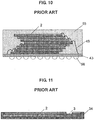
- As a method of manufacturing a semiconductor device such as an LSI unit or an IC module, as shown in
Fig. 10 , there is a method of manufacturing a Stacked MCP (Multi Chip Package) which is obtained by foremost facing the circuit surfaces of a plurality ofsemiconductor elements 2 determined as non-defective in electrical property testing, in the same direction and stackingsuch semiconductor elements 2 on asupport substrate 43 in a manner where the electrode pads (not shown) of the respective semiconductor elements are exposed without being hidden by the other semiconductor elements, electrically connecting the electrode pads of the semiconductor elements and thesupport substrate 43 via awire bonding 46, thereafter sealing the product with asealing resin 55, formingsolder balls 56 as external connecting terminals, and individually cutting the semiconductor elements to complete the semiconductor devices (for instance, refer to Japanese Patent Application Publication No.2002-33442 - Nevertheless, with a conventional semiconductor device obtained as described above, since only one side or both sides of the semiconductor element can be electrically connected with the support substrate since a wire bonding is used for the connection, there is a limit in that only two semiconductor elements can be simultaneously operated.
- Moreover, there are demands for thinning the package in which a plurality of semiconductor elements are stacked, and in order to meet such demands, it is necessary to reduce the thickness of each semiconductor element and mount such thin semiconductor elements, and reduce the height of the connecting members such as a wire bonding.
- Nevertheless, the connection of the wire bonding to be connected to the semiconductor element needs to pass above the mounted semiconductor element, but if the height of the connecting member is low, it will connect with the semiconductor element and cause a short-circuit.
- Thus, in order to prevent the portions other than the electrodes of the semiconductor element from contacting the wire bonding, as shown in
Fig. 11 , aninsulating material layer 34 as a protective resin layer is formed on a part of the electrode-forming part or the side face or back face of thesemiconductor element 2 in order to prevent short-circuits (for instance, refer to Japanese Patent Application Publication No.2009-49118 - When simultaneously operating more than two semiconductor elements, it is necessary to stack the semiconductor elements so as to be directly connected with the two semiconductor elements to be operated for simultaneous operation with the two semiconductor elements. Thus, the size of the semiconductor device becomes large, and the junction temperatures in the semiconductor elements will increase due to the poor heat radiation of the stacked structure, thereby causing a problem in that the foregoing simultaneous operation is not possible.
- As recent trends, the downsizing of the semiconductor package size and the increase in the number of semiconductor elements that can be mounted are being demanded. In order to meet these demands, the following have been proposed and developed; namely, a semiconductor device having a POP (Package on Package) structure in which another semiconductor package or a circuit board is stacked on a semiconductor package (Japanese Patent Application Publication No.
2008-218505 2010-278334 - A conventional POP structure semiconductor device is now explained based on
Fig. 8 . POP (Package on Package) is a package mode in which a plurality of different LSIs are assembled as individual packages, tested, and then stacking the packages thereafter. - The
semiconductor device 40 is configured by anothersemiconductor package 42 being stacked on asemiconductor package 41. Asemiconductor element 44 is mounted on thesubstrate 43 of thelower semiconductor package 41, and electrode pads (not shown) formed at the periphery of thesemiconductor element 44 andelectrode pads 45 on the substrate are electrically connected viawires 46. The entire surface of thesemiconductor element 44 is sealed with a sealingmember 47. In addition, thesemiconductor package 41 and thesemiconductor package 42 are mutually electrically connected based on reflow via external connecting terminals 48 (solder balls) formed on the lower face of thesemiconductor package 42. - POP is advantageous in that the mounting area can be increased upon mounting devices as a result of stacking a plurality of packages as described above, and, since each package can be individually tested, the production yield loss can be reduced. Nevertheless, with POP, since the individual packages are individually assembled and the completed packages are stacked, it is difficult to reduce the assembly costs based on the reduction (shrinkage) of the semiconductor element size, and there is a problem in that the assembly cost of the stacked module is extremely expensive.
- A conventional TSV structure semiconductor device is now explained with reference to
Fig. 9 . As shown inFig. 9 , asemiconductor device 50 has a structure in which a plurality ofsemiconductor elements 51 mutually have the same function and structure and which are respectively prepared using the same manufacture mask and oneinterposer substrate 52 are stacked via aresin layer 53. Eachsemiconductor element 51 is a semiconductor element using a silicon substrate, and is electrically connected to the upper and lower adjacent semiconductor elements via multiple through electrodes (TSV: Through Silicon Via) 54 that penetrate the silicon substrate and sealed with sealingresin 55. Meanwhile, theinterposer substrate 52 is a circuit board made of resin, and a plurality of external connecting terminals (solder balls) 56 are formed on the back face thereof. - With a conventional TSV (Through Silicon Via) stacked module structure, since through-holes are provided to each of the individual semiconductor elements, there is a possibility that the semiconductor element will become damaged, and it is also necessary to add several complex and costly wafer processes of forming via electrodes in the through-holes. Thus, this resulted in a considerable cost increase of the overall vertically stacked module. Moreover, with the conventional structure, it is difficult to stack and mount chips of different sizes, and, due to the "addition of different rewiring layers for each layer" which is essential upon lamination of the same chips as in a memory device, the manufacture costs increase considerably in comparison to ordinary memory device modules, and there is a problem in that the cost reduction based on mass production cannot be expected.
-
EP 1 367 645 A2 -
US 2009/0134528 A1 discloses a semiconductor package, an electronic device including the semiconductor package and a method of manufacturing the semiconductor package. The semiconductor package includes semiconductor chips mounted on a carrier, a first insulating layer sealing the semiconductor chips, first via-holes which are formed in the first insulating layer and expose a portion of each of the semiconductor chips, a first conductive pattern which is filled in the first via-holes and electrically connected to each of the semiconductor chips, and an external terminal which is electrically connected to the first conductive pattern. The semiconductor package is manufactured by performing an encapsulating process and a via-hole process. -
US 2010/0193930 A1 discloses that a multi-chip device can have a plurality of chips in a stair-step arrangement having respective chip pads thereon. A mold packaging material encapsulates the plurality of chips and at least one conductive via, that is in the mold packaging material and extends from an outer surface of the material, contacts a respective one of the chip pads. A conductive material is in the at least one conductive via. - The scope of the invention is defined in the appended claims. Any reference to "embodiment(s)", "example(s)" or "aspect(s) of the invention" in this description not falling under the scope of the claims should be interpreted as illustrative example(s) for understanding the invention.
- An object of this invention is to provide a semiconductor device and its manufacturing method which can achieve a smaller and thinner semiconductor device and considerably reduce the number of manufacturing steps by causing a plurality of semiconductor chips to be a vertically-stacked structure.
- In order to achieve the foregoing object, the present inventors completed the present invention by discovering that the foregoing object can be achieved with the following configuration; namely, by adopting, as a unit structure component, a structure including a semiconductor element, an insulating material layer for sealing the semiconductor element and periphery thereof, a metal thin film wiring layer provided in the insulating material layer , with a part thereof being exposed on an external surface, and metal vias provided in the insulating material layer and which are electrically connected to the metal thin film wiring layer, wherein the semiconductor element is provided in a plurality, and the respective semiconductor elements are stacked via an insulating material such that a circuit surface of each semiconductor element faces the metal thin film wiring layer, and wherein electrode pads of each semiconductor element are exposed without being hidden by the semiconductor element stacked thereabove, and electrically connected to the metal thin film wiring layer.
-
-
Fig. 1 is adiagram showing Embodiment 1 of the semiconductor device of the present invention. -
Figs. 2A and 2B are diagrams each showing a stacking example upon stacking the semiconductor elements. -
Figs. 3A to 3T are a diagram showing the steps of the method of manufacturing the semiconductor device ofEmbodiment 1. -
Fig. 4 is adiagram showing Embodiment 2 of the semiconductor device of the present invention. -
Fig. 5 is adiagram showing Embodiment 3 of the semiconductor device of the present invention. -
Fig. 6 is a cross-sectional view showing an example of the semiconductor device as a reference example. -
Figs. 7A to 7S are a diagram showing the steps of the method of manufacturing the semiconductor device illustrated inFig. 6 . -
Fig. 8 is a diagram showing the structure of a conventional POP structure semiconductor device. -
Fig. 9 is a diagram showing the structure of a conventional TSV structure semiconductor device. -
Fig. 10 is a diagram showing the structure of a semiconductor device as a conventional LSI unit or IC module. -
Fig. 11 is a diagram showing the structure for preventing short-circuits in a conventional semiconductor element. - Upon completing the present invention, the present inventors examined a semiconductor device to become a prototype of this invention and the manufacturing method thereof. Since the features of the present invention will become more evident by way of comparison with the prototype semiconductor device and the manufacturing method thereof, this prototype semiconductor device (hereinafter referred to as "Semiconductor Device D") is taken as a reference example hereinafter and foremost explained.
-
Fig. 6 is a diagram showing the structure of Semiconductor Device D. This Semiconductor Device D is structured by stacking a plurality of unit structure components, wherein each unit structure component is configured from asemiconductor element 2, an insulatingmaterial layer 4 for sealing thesemiconductor element 2 and its periphery, a metal thinfilm wiring layer 6 provided in the insulatingmaterial layer 4, and via 9 provided in the insulatingmaterial layer 4 and electrically connected to the metal thinfilm wiring layer 6, wherein the illustrated structure is configured by stacking eight semiconductor elements. - The manufacturing method of this Semiconductor Device D is now explained with reference to
Figs. 7A to 7S. Figs. 7A to 7S respectively illustrate steps (a) to (s) of the manufacturing method of Semiconductor Device D, and the respective steps are explained below. - A
semiconductor element 2, which was determined as being non-defective in electrical property testing, is fixed on asupport substrate 1, via an adhesive, with the circuit surface thereof facing up. - Insulating resin is supplied around the
semiconductor element 2 fixed on the support substrate to form an insulating material layer 4 (insulating material layer a) . -
Openings 5 are formed in the insulating material layer on theelectrode pads 3 for causing the electrode pads of thesemiconductor element 2 to be exposed from the insulatingmaterial layer 4. - A metal thin film seed layer (underlayer) is formed on the entire upper surface of the insulating
material layer 4 with theopenings 5 by the vapor deposition method (sputtering), electroless plating or the like. - In order to form a metal thin film wiring layer onto the predetermined areas of the insulating
material layer 4 with the seed layer formed thereon, a plating resist is formed and a conductive metal thin film wiring layer is formed on the areas, where the plating resist is removed via patterning, of the insulatingmaterial layer 4, by electrolytic plating. Theopenings 5 are filled with a conductive metal. - After forming the metal thin
film wiring layer 6, the plating resist at areas where the wiring layer is not formed and the seed layer (underlayer) below the plating resist are removed via etching. - An insulating material layer 7 (insulating material layer b) is formed on the surface of the insulating
material layer 4 with the metal thinfilm wiring layer 6 formed thereon. - A
semiconductor element 2, which was determined as being non-defective in electrical property testing, is fixed on the insulating material layer 7 (insulating material layer b), via an adhesive, with the circuit surface thereof facing up so as to mount thesemiconductor element 2 on the insulatingmaterial layer 7. - Insulating resin is supplied around the
semiconductor element 2 fixed on the insulatingmaterial layer 7 to form an insulating material layer 4 (insulating material layer a), and thesemiconductor element 2 is thereby resin-sealed. -
Openings 8 for forming vias andopenings 5 for exposing the electrode pads of thesemiconductor element 2 are formed on the insulatingmaterial layer 4. - A metal thin film seed layer (underlayer) is formed on the entire upper surface of the insulating
material layer 4 with theopenings 5 and theopenings 8 formed thereon via a vapor deposition method (sputtering), electroless plating or the like. - In order to form a metal thin film wiring layer onto the predetermined areas of the insulating
material layer 4 with the seed layer formed thereon, a plating resist is formed and the metal thin film wiring layer is formed on the areas, where the plating resist is removed via patterning, of the insulatingmaterial layer 4, by electrolytic plating. Theopenings - After forming the metal thin
film wiring layer 6, the plating resist at areas where the wiring layer is not formed and the seed layer (underlayer) below the plating resist are removed via etching. - An insulating material layer 7 (insulating material layer b) is formed on the surface of the insulating
material layer 4 with the metal thinfilm wiring layer 6 formed thereon. - The steps of foregoing (h) to (n) are repeated six times. It is thereby possible to obtain the structure shown in
Fig. 6 where eight semiconductor elements are stacked. - In order to protect the wirings, a wiring protective film (resist layer) 10 such as a solder resist is formed on the surface of the metal thin film wiring layer. The solder resist is supplied with a roll coater when the solder resist is in a liquid form, and supplied by lamination or bonding press when the solder resist is of a film shape.
- In order to electrically connect the semiconductor device with a semiconductor package or an electronic component, resist
openings 11 for providing external metal electrodes to predetermined positions corresponding to thevias 9 are formed in the wiring protective film. - A terminal plating 12 for providing external metal electrodes or an organic protective film is formed on the resist
openings 11. - External metal electrodes (
solder balls 13 in the illustrated example) made of a conductive material are formed on the terminal plating. As the conductive material, conductive materials such as solder balls, conductive paste, solder paste and the like are used. - The semiconductor device (multi chip package) obtained as described above is divided into individual pieces, whereby the semiconductor devices are completed.
- The foregoing manufacturing method has a problem in that one metal thin film wiring layer needs to be formed for each semiconductor element, and the number of steps thereby increases.
- Thus, as a result of adopting a structure of electrically connecting a plurality of semiconductor elements to one metal thin film wiring layer, the present inventors enables the simplification of the manufacture step of the semiconductor device, and the downsizing of the semiconductor device.
- This semiconductor device is now explained with reference to the embodiments.
-
Fig. 1 is a diagram showing the configuration of Semiconductor Device A ofEmbodiment 1 of the present invention. - As shown in the diagram, this Semiconductor Device A includes
semiconductor elements material layer 4 for sealing thesemiconductor elements film wiring layer 6 provided in the insulatingmaterial layer 7 and in which a part thereof is exposed on the external surface, andmetal vias 9 provided in the insulating material layer and electrically connected to the metal thin film wiring layer.Reference numeral 1 represents a metal support substrate. - In addition, the two
semiconductor elements material layer 4, and the structure is such that one metal thinfilm wiring layer 6 is provided to the two semiconductor elements. - The two
semiconductor elements film wiring layer 6, and the electrode pads of therespective semiconductor elements - When the two
semiconductor elements Fig. 2A , there is a method of opposing the direction of semiconductor chips of the same size and stacking the semiconductor elements so that the electrode pads of the lower semiconductor element are exposed, or, as shown inFig. 2B , using semiconductor elements of different sizes and stacking the semiconductor elements so that the electrode pads of the lower semiconductor element is exposed. - The manufacturing step of Semiconductor Device A of
Embodiment 1 is now explained in detail with reference toFigs. 3A to 3T which respectively illustrate steps (A) to (T) described below. - A
first semiconductor element 2a, determined as non-defective in electrical property testing, is fixed on asupport substrate 1, via an adhesive, with the circuit surface thereof facing up. In addition, asecond semiconductor element 2b is fixed on the first semiconductor element via an adhesive, with the circuit surface of the second semiconductor element facing up, so that the electrode pads of the first semiconductor element are exposed.Reference numeral 14 is a die attach. - Insulating resin is supplied around the
semiconductor elements metal support substrate 1 to form an insulating material layer 4 (insulating material layer a). Thermosetting resin is used as the insulating resin, but photosensitive resin may also be used. - Thermosetting resin may be used as the insulating material layer around the semiconductor elements, and a photosensitive resin layer may be used as the layer thereabove. Consequently, the enhancing effect of the sealing reliability for the semiconductor elements by the thermosetting resin layer and the enhancing effect of the patterning properties by the photosensitive resin layer can be expected.
-
Openings 5 are formed in the insulating material layer on theelectrode pads 3 for causing theelectrode pads 3 of thesemiconductor elements material layer 4, andopenings 8 for forming vias are also formed in the insulatingmaterial layer 4. - The
openings openings openings - A thin metal film seed layer (underlayer) is formed on the entire upper surface of the insulating
material layer 4 having theopenings - In order to form a wiring layer on the upper face of the insulating
material layer 4 with the seed layer formed thereon, a plating resist is formed and a conductive metal thinfilm wiring layer 6 is formed on the insulatingmaterial layer 4, via electrolytic plating, at areas where the plating resist is removed via patterning, and theopenings openings 8 filled with the conductive material. - After forming the metal thin
film wiring layer 6, the plating resist at areas where the wiring layer is not formed and the seed layer (underlayer) below the resist are removed via etching. - An insulating material layer 7 (insulating material layer b) is formed on the surface of the insulating
material layer 4 with the metal thinfilm wiring layer 6 formed thereon. -
Openings 8 are formed in the insulatingmaterial layer 7 positioned above thevias 9 for securing the electrical connection of thevias 9. - The
semiconductor elements semiconductor elements material layer 7. - Insulating resin is supplied around the
semiconductor elements material layer 7 to form an insulating material layer 4 (insulating material layer a), and thesemiconductor elements - For the insulating
material layer 7,openings 8 for forming vias andopenings 5 for exposing the electrode pads of thesemiconductor elements material layer 4. The processing method is as described in the foregoing step of (C). - A seed layer (underlayer) is formed on the entire upper surface of the insulating
material layer 4 with theopenings 5 and theopenings 8 formed therein via a vapor deposition method (sputtering), electroless plating or the like. - In order to form a wiring layer on the upper face of the insulating
material layer 4 with the seed layer formed thereon, a plating resist is formed and a metal thinfilm wiring layer 6 is formed on the insulatingmaterial layer 4 at areas where the resist is removed via patterning, via electrolytic plating. Moreover, theopenings 8 are filled with the conductive metal, whereby thevias 9 are formed, and theopenings 5 is filled with the conductive metal. - After forming the metal thin
film wiring layer 6, the plating resist at the areas, where the wiring layer is not formed, and the seed layer (underlayer) under the resist at the areas are removed via etching. - An insulating material layer 7 (insulating material layer b) is formed on the surface of the insulating
material layer 4 with the metal thinfilm wiring layer 6 formed thereon. - The steps of foregoing (H) to (O) are repeated twice. It is thereby possible to obtain the structure shown in
Fig. 1 where eight semiconductor elements are stacked. - In order to protect the wirings, a wiring protective film (resist layer) 10 such as a solder resist is formed on the surface of the metal thin film wiring layer. The solder resist is supplied with a roll coater when the solder resist is in a liquid form, and supplied via lamination or bonding press when the solder resist is of a film shape.
- In order to electrically connect the semiconductor device with a semiconductor package or an electronic component, resist
openings 11 for providing external metal electrodes to predetermined positions corresponding to thevias 9 are formed. - A terminal plating 12 for providing external metal electrodes or an organic protective film is formed on the resist
openings 11. - External metal electrodes 13 (
solder balls 13 in the illustrated example) made of a conductive material are formed on the terminal plating. As the conductive material, conductive materials such as a solder ball, conductive paste, solder paste and the like are used. - Normally, a plurality of semiconductor devices are simultaneously formed in the vertical direction and horizontal direction on a large-area support substrate. In this case, after the
external electrodes 13 are formed, the obtained multi chip package is cut into individual pieces, whereby the semiconductor devices are completed. - While the semiconductor A shown in
Fig. 1 is structured by stacking eight semiconductor elements, as a result of repeating the steps (H) to (O) shown inFigs. 3H to 3O , it is possible to manufacture a semiconductor device in which more than eight semiconductor elements are stacked. While in the above case of Semiconductor Device A, the semiconductor elements used in each stacked body as a unit structure component are all shown with thesame reference numerals - Semiconductor Device B of
Embodiment 2,uses an organic support substrate 1' in substitute for themetal support substrate 1 in the Semiconductor Device A ofEmbodiment 1 as shown inFig. 4 . - While the metal support substrate is advantageous in terms of heat-release properties and that it can be connected to GND, there are drawbacks in that the workability is inferior and hole-making is difficult, and it is difficult to provide insulation. Thus, it is difficult to mount another semiconductor package or electronic component on the metal support substrate.
- Meanwhile, an organic support substrate made from an organic compound material such as glass-reinforced epoxy resin is advantageous, in comparison to a metal support substrate, in terms of favorable workability such as hole-making, and having insulating properties. Thus, as shown in
Fig. 4 , as a result of opening through-holes and providing electrical connection parts, it is possible to mount passive components such as a semiconductor package or capacitor on the semiconductor device. - With Semiconductor Device C of
Embodiment 3, as shown inFig. 5 , the organic support substrate 1' used inEmbodiment 2 is provided to thesolder balls 13 mounting side. - This structure is able to achieve a face-up structure (semiconductor element circuit surfaces face the mounting face) as in the case of using wires for wiring, and it is easy to achieve the same terminal arrangement as in
Embodiment 2. - Moreover, there is also an advantage in that the lower side is compatible with the motherboard since it is the organic support substrate.
Claims (9)
- A semiconductor unit structure component, comprising:a support substrate (1, 1') and on the support substrate a plurality of semiconductor elements (2a, 2b);a first insulating material layer (4) for sealing the semiconductor elements (2a,2b) and a periphery thereof;a metal thin film wiring layer (6) provided on the first insulating material layer (4), a second insulating material layer (7) provided on and covering both the surface of the metal thin film wiring layer (6) and the surface of the part of the first insulating material layer (4) which is not the metal thin film wiring layer (6),metal vias (9) provided in the first insulating material layer (4) and connecting from the support substrate (1, 1') to the metal thin film wiring layer (6),an opening (5) which is formed in the second insulating material layer (7) positioned above the vias (9) for securing the electrical connection of the metal vias (9) on an external surface; and for exposing a part of the metal thin film wiring layer (6) on the external surface, andan electrode pad connecting via provided on electrode pads (3) of the semiconductor elements (2a, 2b) in the first insulating material layer (4), whereinthe semiconductor elements (2a, 2b) are stacked via an adhesive such that a circuit surface of each semiconductor elements face the metal thin film wiring layer (6), andthe electrode pads (3) of each semiconductor element (2a) are exposed without being hidden by the semiconductor element (2b) stacked there above, and the electrode pad connecting via is electrically connected to the electrode pads (3) and the metal thin film wiring layer (6).
- A semiconductor device, comprising a plurality of semiconductor unit structure components stacked on a support substrate (1, 1'), wherein each semiconductor unit structure component comprises the stacked semiconductor unit structure component provided on the support substrate as described in claim 1, and
wherein the respective semiconductor unit structure components are electrically connected by the metal vias (9). - The semiconductor device according to claim 2, wherein the first insulating material layer (4) is formed of a plurality of insulating material layers made of respectively different insulating materials.
- The semiconductor device according to any one of claims 2 to 3, wherein the first insulating material layer is composed of a photosensitive resin layer and a thermosetting resin layer.
- The semiconductor device according to any one of claims 2 to 4,
wherein the support substrate (1) is made of a metal material, and the support substrate is connected to a GND - The semiconductor device according to any one of claims 2 to 4,
wherein the support substrate (1, 1') is made of an organic material or made of an organic material and a metal conductor. - The semiconductor device according to claim 6, wherein other semiconductor package or electronic component is stacked via the support substrate (1, 1'), and the semiconductor device is electrically connected to the other semiconductor package or electronic component via external metal electrodes (13) mounted on through-holes provided to the support substrate (1, 1').
- A method of manufacturing the semiconductor unit structure component according to claim 1,comprising the steps of:stacking and fixing, on the support substrate, a plurality of semiconductor elements (2a, 2b) via an insulating material such that circuit surfaces thereof face a same direction, and electrode pads (3) of each semiconductor element (2a) are exposed without being hidden by the other semiconductor element (2b);forming a first insulating material layer (4) for sealing the semiconductor elements (2a, 2b) and peripheries thereof;forming, in the first insulating material layer (4), openings (8) for forming metal vias (9) and openings (5) for electrically connecting the electrode pads (3);forming a metal thin film seed layer on the first insulating material layer surface;filling a conductive material in the openings (5, 8) and forming a metal thin film wiring layer (6) at predetermined areas on the metal thin film seed layer;removing the metal thin film seed layer on the first insulating material layer surface except the areas where the metal thin film wiring layer (6) is formed; andforming a second insulating material layer (7) on the first insulating material layer (4) provided thereon with the metal thin film wiring layer (6) and forming openings (8) in the second insulating material layer (7) positioned above the metal vias (9) for securing the electrical connection of the metal vias (9).
- A method of manufacturing the semiconductor device as described in claim 2,
wherein a plurality of the semiconductor unit structure components are mounted on the support substrate by repeating, on the second insulating layer (7), the series of steps as described in claim 8,
wherein the respective semiconductor unit structure components are electrically connected by the metal vias (9).
Applications Claiming Priority (1)
| Application Number | Priority Date | Filing Date | Title |
|---|---|---|---|
| JP2012025042A JP5912616B2 (en) | 2012-02-08 | 2012-02-08 | Semiconductor device and manufacturing method thereof |
Publications (3)
| Publication Number | Publication Date |
|---|---|
| EP2634796A2 EP2634796A2 (en) | 2013-09-04 |
| EP2634796A3 EP2634796A3 (en) | 2015-03-25 |
| EP2634796B1 true EP2634796B1 (en) | 2020-04-08 |
Family
ID=47221945
Family Applications (1)
| Application Number | Title | Priority Date | Filing Date |
|---|---|---|---|
| EP12189403.4A Active EP2634796B1 (en) | 2012-02-08 | 2012-10-22 | Semiconductor device and manufacturing method thereof |
Country Status (6)
| Country | Link |
|---|---|
| US (1) | US8872350B2 (en) |
| EP (1) | EP2634796B1 (en) |
| JP (1) | JP5912616B2 (en) |
| KR (1) | KR101653856B1 (en) |
| CN (1) | CN103247599B (en) |
| TW (1) | TWI557868B (en) |
Families Citing this family (20)
| Publication number | Priority date | Publication date | Assignee | Title |
|---|---|---|---|---|
| JP2611150B2 (en) | 1994-10-13 | 1997-05-21 | 株式会社ドーセン | Cement-based artificial wood composition |
| JP2014082245A (en) | 2012-10-15 | 2014-05-08 | J Devices:Kk | Semiconductor storage device and method of manufacturing the same |
| JP6377894B2 (en) * | 2013-09-03 | 2018-08-22 | 信越化学工業株式会社 | Manufacturing method of semiconductor device, manufacturing method of stacked semiconductor device, and manufacturing method of stacked semiconductor device after sealing |
| JP6961885B2 (en) * | 2013-09-27 | 2021-11-05 | インテル・コーポレーション | Semiconductor assembly and manufacturing method of semiconductor assembly |
| KR102052255B1 (en) | 2013-09-27 | 2019-12-04 | 인텔 코포레이션 | Method for interconnecting stacked semiconductor devices |
| CN104517934B (en) * | 2013-09-27 | 2017-09-12 | 英特尔公司 | Method for interconnecting stacked semiconductor devices |
| JP6331452B2 (en) * | 2014-02-19 | 2018-05-30 | 愛知製鋼株式会社 | Etching method of organic film |
| KR102186150B1 (en) * | 2014-07-29 | 2020-12-03 | 삼성전기주식회사 | Printed circuit board using the insulating film and method for manufacturing the same |
| US9984191B2 (en) | 2014-08-29 | 2018-05-29 | Taiwan Semiconductor Manufacturing Company | Cell layout and structure |
| US9609749B2 (en) | 2014-11-14 | 2017-03-28 | Mediatek Inc. | Printed circuit board having power/ground ball pad array |
| JP6537815B2 (en) * | 2014-12-11 | 2019-07-03 | 株式会社ジェイデバイス | Semiconductor package and method of manufacturing the same |
| US9832866B2 (en) * | 2015-06-29 | 2017-11-28 | Samsung Electro-Mechanics Co., Ltd. | Multilayered substrate and method of manufacturing the same |
| US10455708B2 (en) | 2015-06-29 | 2019-10-22 | Samsung Electro-Mechanics Co., Ltd. | Multilayered substrate and method for manufacturing the same |
| WO2018051800A1 (en) * | 2016-09-16 | 2018-03-22 | 株式会社大真空 | Piezoelectric vibration device |
| KR102564324B1 (en) | 2018-10-15 | 2023-08-07 | 삼성전자주식회사 | Apparatus of semiconductor memory and method of manufacturing the same |
| JP2020150026A (en) * | 2019-03-11 | 2020-09-17 | 株式会社村田製作所 | Multi-layer wiring board |
| KR102302563B1 (en) | 2019-12-05 | 2021-09-15 | 고려대학교 산학협력단 | Method for forming via on element, method of manufacturing semiconductor element based on the same and the semiconductor thereof |
| US11211310B1 (en) * | 2020-09-03 | 2021-12-28 | Delta Electronics, Inc. | Package structures |
| CN112968012B (en) * | 2021-02-01 | 2022-09-09 | 长江存储科技有限责任公司 | Fan-out chip stack package structure and manufacturing method thereof |
| EP4401078B1 (en) * | 2022-11-25 | 2025-01-15 | Yangtze Memory Technologies Co., Ltd. | Chip packaging structure and manufacturing method therefor, and electronic device |
Family Cites Families (22)
| Publication number | Priority date | Publication date | Assignee | Title |
|---|---|---|---|---|
| US5068714A (en) * | 1989-04-05 | 1991-11-26 | Robert Bosch Gmbh | Method of electrically and mechanically connecting a semiconductor to a substrate using an electrically conductive tacky adhesive and the device so made |
| US5032896A (en) * | 1989-08-31 | 1991-07-16 | Hughes Aircraft Company | 3-D integrated circuit assembly employing discrete chips |
| JP3818359B2 (en) | 2000-07-18 | 2006-09-06 | セイコーエプソン株式会社 | Semiconductor device, circuit board and electronic equipment |
| WO2003067656A1 (en) * | 2002-02-06 | 2003-08-14 | Ibiden Co., Ltd. | Semiconductor chip mounting board, its manufacturing method, and semiconductor module |
| EP2866258B1 (en) * | 2002-05-31 | 2019-04-17 | Socionext Inc. | Semiconductor device and manufacturing method thereof |
| JP3801158B2 (en) * | 2002-11-19 | 2006-07-26 | セイコーエプソン株式会社 | MULTILAYER WIRING BOARD MANUFACTURING METHOD, MULTILAYER WIRING BOARD, ELECTRONIC DEVICE, AND ELECTRONIC DEVICE |
| KR100537892B1 (en) * | 2003-08-26 | 2005-12-21 | 삼성전자주식회사 | Chip stack package and manufacturing method thereof |
| TWI222734B (en) * | 2003-10-03 | 2004-10-21 | Thin Film Module Inc | High density module card, substrate and fabrication for the same |
| JP4340517B2 (en) * | 2003-10-30 | 2009-10-07 | Okiセミコンダクタ株式会社 | Semiconductor device and manufacturing method thereof |
| JP4403407B2 (en) * | 2005-02-03 | 2010-01-27 | ソニー株式会社 | Semiconductor device and manufacturing method thereof |
| JP4507101B2 (en) * | 2005-06-30 | 2010-07-21 | エルピーダメモリ株式会社 | Semiconductor memory device and manufacturing method thereof |
| JP4843515B2 (en) * | 2007-02-01 | 2011-12-21 | パナソニック株式会社 | Stacked structure of semiconductor chips |
| JP5135828B2 (en) | 2007-02-28 | 2013-02-06 | ソニー株式会社 | Substrate and manufacturing method thereof, semiconductor package and manufacturing method thereof, and semiconductor device and manufacturing method thereof |
| JP5143451B2 (en) * | 2007-03-15 | 2013-02-13 | オンセミコンダクター・トレーディング・リミテッド | Semiconductor device and manufacturing method thereof |
| KR100845006B1 (en) * | 2007-03-19 | 2008-07-09 | 삼성전자주식회사 | Laminated chip package and its manufacturing method |
| JP4496241B2 (en) | 2007-08-17 | 2010-07-07 | 株式会社東芝 | Semiconductor device and semiconductor package using the same |
| KR20090055316A (en) * | 2007-11-28 | 2009-06-02 | 삼성전자주식회사 | Semiconductor package, method for manufacturing electronic device and semiconductor package having same |
| JP4538058B2 (en) * | 2008-03-28 | 2010-09-08 | 株式会社東芝 | Integrated semiconductor device and integrated three-dimensional semiconductor device |
| US20100193930A1 (en) * | 2009-02-02 | 2010-08-05 | Samsung Electronics Co., Ltd. | Multi-chip semiconductor devices having conductive vias and methods of forming the same |
| JP2010278334A (en) | 2009-05-29 | 2010-12-09 | Elpida Memory Inc | Semiconductor device |
| US8169065B2 (en) * | 2009-12-22 | 2012-05-01 | Epic Technologies, Inc. | Stackable circuit structures and methods of fabrication thereof |
| JP2010232702A (en) * | 2010-07-20 | 2010-10-14 | Toshiba Corp | Multilayer semiconductor device |
-
2012
- 2012-02-08 JP JP2012025042A patent/JP5912616B2/en active Active
- 2012-09-14 US US13/616,549 patent/US8872350B2/en active Active
- 2012-09-20 TW TW101134430A patent/TWI557868B/en active
- 2012-10-18 CN CN201210397451.4A patent/CN103247599B/en active Active
- 2012-10-22 EP EP12189403.4A patent/EP2634796B1/en active Active
- 2012-11-14 KR KR1020120128794A patent/KR101653856B1/en active Active
Non-Patent Citations (1)
| Title |
|---|
| None * |
Also Published As
| Publication number | Publication date |
|---|---|
| JP2013162071A (en) | 2013-08-19 |
| KR101653856B1 (en) | 2016-09-02 |
| CN103247599A (en) | 2013-08-14 |
| EP2634796A3 (en) | 2015-03-25 |
| KR20130091624A (en) | 2013-08-19 |
| TWI557868B (en) | 2016-11-11 |
| US8872350B2 (en) | 2014-10-28 |
| JP5912616B2 (en) | 2016-04-27 |
| CN103247599B (en) | 2017-07-21 |
| US20130200523A1 (en) | 2013-08-08 |
| EP2634796A2 (en) | 2013-09-04 |
| TW201334143A (en) | 2013-08-16 |
Similar Documents
| Publication | Publication Date | Title |
|---|---|---|
| EP2634796B1 (en) | Semiconductor device and manufacturing method thereof | |
| TWI851814B (en) | Semiconductor package | |
| US8889484B2 (en) | Apparatus and method for a component package | |
| EP2551904A1 (en) | Semiconductor device, semiconductor module structure configured by vertically stacking semiconductor devices, and manufacturing method thereof | |
| KR101983186B1 (en) | Fan-out semiconductor package | |
| US7993979B2 (en) | Leadless package system having external contacts | |
| US8861221B2 (en) | Integrated circuit packaging system with a shield and method of manufacture thereof | |
| US7514770B2 (en) | Stack structure of carrier board embedded with semiconductor components and method for fabricating the same | |
| US20120049366A1 (en) | Package structure having through-silicon-via (tsv) chip embedded therein and fabrication method thereof | |
| KR20190005697A (en) | Fan-out semiconductor package module | |
| KR101892903B1 (en) | Fan-out semiconductor package | |
| US9917073B2 (en) | Reconstituted wafer-level package dram with conductive interconnects formed in encapsulant at periphery of the package | |
| US11114412B2 (en) | Electronic package and method for fabricating the same | |
| US9196507B1 (en) | Semiconductor device, semiconductor stacked module structure, stacked module structure and method of manufacturing same | |
| US20070052082A1 (en) | Multi-chip package structure | |
| EP2903021A1 (en) | Semiconductor device, semiconductor stacked module structure, stacked module structure and method of manufacturing same | |
| US20260005111A1 (en) | Semiconductor packaging method, semiconductor package and electronic device | |
| KR102736602B1 (en) | Semiconductor packages and method of manufacturing semiconductor packages |
Legal Events
| Date | Code | Title | Description |
|---|---|---|---|
| PUAI | Public reference made under article 153(3) epc to a published international application that has entered the european phase |
Free format text: ORIGINAL CODE: 0009012 |
|
| AK | Designated contracting states |
Kind code of ref document: A2 Designated state(s): AL AT BE BG CH CY CZ DE DK EE ES FI FR GB GR HR HU IE IS IT LI LT LU LV MC MK MT NL NO PL PT RO RS SE SI SK SM TR |
|
| AX | Request for extension of the european patent |
Extension state: BA ME |
|
| PUAL | Search report despatched |
Free format text: ORIGINAL CODE: 0009013 |
|
| AK | Designated contracting states |
Kind code of ref document: A3 Designated state(s): AL AT BE BG CH CY CZ DE DK EE ES FI FR GB GR HR HU IE IS IT LI LT LU LV MC MK MT NL NO PL PT RO RS SE SI SK SM TR |
|
| AX | Request for extension of the european patent |
Extension state: BA ME |
|
| RIC1 | Information provided on ipc code assigned before grant |
Ipc: H01L 21/98 20060101ALI20150219BHEP Ipc: H01L 23/538 20060101AFI20150219BHEP |
|
| 17P | Request for examination filed |
Effective date: 20150917 |
|
| RBV | Designated contracting states (corrected) |
Designated state(s): AL AT BE BG CH CY CZ DE DK EE ES FI FR GB GR HR HU IE IS IT LI LT LU LV MC MK MT NL NO PL PT RO RS SE SI SK SM TR |
|
| STAA | Information on the status of an ep patent application or granted ep patent |
Free format text: STATUS: EXAMINATION IS IN PROGRESS |
|
| 17Q | First examination report despatched |
Effective date: 20180606 |
|
| GRAP | Despatch of communication of intention to grant a patent |
Free format text: ORIGINAL CODE: EPIDOSNIGR1 |
|
| STAA | Information on the status of an ep patent application or granted ep patent |
Free format text: STATUS: GRANT OF PATENT IS INTENDED |
|
| INTG | Intention to grant announced |
Effective date: 20191023 |
|
| GRAS | Grant fee paid |
Free format text: ORIGINAL CODE: EPIDOSNIGR3 |
|
| GRAA | (expected) grant |
Free format text: ORIGINAL CODE: 0009210 |
|
| STAA | Information on the status of an ep patent application or granted ep patent |
Free format text: STATUS: THE PATENT HAS BEEN GRANTED |
|
| AK | Designated contracting states |
Kind code of ref document: B1 Designated state(s): AL AT BE BG CH CY CZ DE DK EE ES FI FR GB GR HR HU IE IS IT LI LT LU LV MC MK MT NL NO PL PT RO RS SE SI SK SM TR |
|
| REG | Reference to a national code |
Ref country code: GB Ref legal event code: FG4D |
|
| REG | Reference to a national code |
Ref country code: CH Ref legal event code: EP Ref country code: AT Ref legal event code: REF Ref document number: 1255519 Country of ref document: AT Kind code of ref document: T Effective date: 20200415 |
|
| REG | Reference to a national code |
Ref country code: DE Ref legal event code: R096 Ref document number: 602012069070 Country of ref document: DE |
|
| REG | Reference to a national code |
Ref country code: IE Ref legal event code: FG4D |
|
| REG | Reference to a national code |
Ref country code: NL Ref legal event code: FP |
|
| REG | Reference to a national code |
Ref country code: LT Ref legal event code: MG4D |
|
| PG25 | Lapsed in a contracting state [announced via postgrant information from national office to epo] |
Ref country code: IS Free format text: LAPSE BECAUSE OF FAILURE TO SUBMIT A TRANSLATION OF THE DESCRIPTION OR TO PAY THE FEE WITHIN THE PRESCRIBED TIME-LIMIT Effective date: 20200808 Ref country code: PT Free format text: LAPSE BECAUSE OF FAILURE TO SUBMIT A TRANSLATION OF THE DESCRIPTION OR TO PAY THE FEE WITHIN THE PRESCRIBED TIME-LIMIT Effective date: 20200817 Ref country code: NO Free format text: LAPSE BECAUSE OF FAILURE TO SUBMIT A TRANSLATION OF THE DESCRIPTION OR TO PAY THE FEE WITHIN THE PRESCRIBED TIME-LIMIT Effective date: 20200708 Ref country code: GR Free format text: LAPSE BECAUSE OF FAILURE TO SUBMIT A TRANSLATION OF THE DESCRIPTION OR TO PAY THE FEE WITHIN THE PRESCRIBED TIME-LIMIT Effective date: 20200709 Ref country code: LT Free format text: LAPSE BECAUSE OF FAILURE TO SUBMIT A TRANSLATION OF THE DESCRIPTION OR TO PAY THE FEE WITHIN THE PRESCRIBED TIME-LIMIT Effective date: 20200408 Ref country code: SE Free format text: LAPSE BECAUSE OF FAILURE TO SUBMIT A TRANSLATION OF THE DESCRIPTION OR TO PAY THE FEE WITHIN THE PRESCRIBED TIME-LIMIT Effective date: 20200408 Ref country code: FI Free format text: LAPSE BECAUSE OF FAILURE TO SUBMIT A TRANSLATION OF THE DESCRIPTION OR TO PAY THE FEE WITHIN THE PRESCRIBED TIME-LIMIT Effective date: 20200408 |
|
| REG | Reference to a national code |
Ref country code: AT Ref legal event code: MK05 Ref document number: 1255519 Country of ref document: AT Kind code of ref document: T Effective date: 20200408 |
|
| PG25 | Lapsed in a contracting state [announced via postgrant information from national office to epo] |
Ref country code: BG Free format text: LAPSE BECAUSE OF FAILURE TO SUBMIT A TRANSLATION OF THE DESCRIPTION OR TO PAY THE FEE WITHIN THE PRESCRIBED TIME-LIMIT Effective date: 20200708 Ref country code: HR Free format text: LAPSE BECAUSE OF FAILURE TO SUBMIT A TRANSLATION OF THE DESCRIPTION OR TO PAY THE FEE WITHIN THE PRESCRIBED TIME-LIMIT Effective date: 20200408 Ref country code: LV Free format text: LAPSE BECAUSE OF FAILURE TO SUBMIT A TRANSLATION OF THE DESCRIPTION OR TO PAY THE FEE WITHIN THE PRESCRIBED TIME-LIMIT Effective date: 20200408 Ref country code: RS Free format text: LAPSE BECAUSE OF FAILURE TO SUBMIT A TRANSLATION OF THE DESCRIPTION OR TO PAY THE FEE WITHIN THE PRESCRIBED TIME-LIMIT Effective date: 20200408 |
|
| PG25 | Lapsed in a contracting state [announced via postgrant information from national office to epo] |
Ref country code: AL Free format text: LAPSE BECAUSE OF FAILURE TO SUBMIT A TRANSLATION OF THE DESCRIPTION OR TO PAY THE FEE WITHIN THE PRESCRIBED TIME-LIMIT Effective date: 20200408 |
|
| REG | Reference to a national code |
Ref country code: DE Ref legal event code: R097 Ref document number: 602012069070 Country of ref document: DE |
|
| PG25 | Lapsed in a contracting state [announced via postgrant information from national office to epo] |
Ref country code: AT Free format text: LAPSE BECAUSE OF FAILURE TO SUBMIT A TRANSLATION OF THE DESCRIPTION OR TO PAY THE FEE WITHIN THE PRESCRIBED TIME-LIMIT Effective date: 20200408 Ref country code: ES Free format text: LAPSE BECAUSE OF FAILURE TO SUBMIT A TRANSLATION OF THE DESCRIPTION OR TO PAY THE FEE WITHIN THE PRESCRIBED TIME-LIMIT Effective date: 20200408 Ref country code: RO Free format text: LAPSE BECAUSE OF FAILURE TO SUBMIT A TRANSLATION OF THE DESCRIPTION OR TO PAY THE FEE WITHIN THE PRESCRIBED TIME-LIMIT Effective date: 20200408 Ref country code: IT Free format text: LAPSE BECAUSE OF FAILURE TO SUBMIT A TRANSLATION OF THE DESCRIPTION OR TO PAY THE FEE WITHIN THE PRESCRIBED TIME-LIMIT Effective date: 20200408 Ref country code: CZ Free format text: LAPSE BECAUSE OF FAILURE TO SUBMIT A TRANSLATION OF THE DESCRIPTION OR TO PAY THE FEE WITHIN THE PRESCRIBED TIME-LIMIT Effective date: 20200408 Ref country code: SM Free format text: LAPSE BECAUSE OF FAILURE TO SUBMIT A TRANSLATION OF THE DESCRIPTION OR TO PAY THE FEE WITHIN THE PRESCRIBED TIME-LIMIT Effective date: 20200408 Ref country code: EE Free format text: LAPSE BECAUSE OF FAILURE TO SUBMIT A TRANSLATION OF THE DESCRIPTION OR TO PAY THE FEE WITHIN THE PRESCRIBED TIME-LIMIT Effective date: 20200408 Ref country code: DK Free format text: LAPSE BECAUSE OF FAILURE TO SUBMIT A TRANSLATION OF THE DESCRIPTION OR TO PAY THE FEE WITHIN THE PRESCRIBED TIME-LIMIT Effective date: 20200408 |
|
| PLBE | No opposition filed within time limit |
Free format text: ORIGINAL CODE: 0009261 |
|
| STAA | Information on the status of an ep patent application or granted ep patent |
Free format text: STATUS: NO OPPOSITION FILED WITHIN TIME LIMIT |
|
| PG25 | Lapsed in a contracting state [announced via postgrant information from national office to epo] |
Ref country code: SK Free format text: LAPSE BECAUSE OF FAILURE TO SUBMIT A TRANSLATION OF THE DESCRIPTION OR TO PAY THE FEE WITHIN THE PRESCRIBED TIME-LIMIT Effective date: 20200408 Ref country code: PL Free format text: LAPSE BECAUSE OF FAILURE TO SUBMIT A TRANSLATION OF THE DESCRIPTION OR TO PAY THE FEE WITHIN THE PRESCRIBED TIME-LIMIT Effective date: 20200408 |
|
| 26N | No opposition filed |
Effective date: 20210112 |
|
| PG25 | Lapsed in a contracting state [announced via postgrant information from national office to epo] |
Ref country code: SI Free format text: LAPSE BECAUSE OF FAILURE TO SUBMIT A TRANSLATION OF THE DESCRIPTION OR TO PAY THE FEE WITHIN THE PRESCRIBED TIME-LIMIT Effective date: 20200408 |
|
| REG | Reference to a national code |
Ref country code: CH Ref legal event code: PL |
|
| PG25 | Lapsed in a contracting state [announced via postgrant information from national office to epo] |
Ref country code: MC Free format text: LAPSE BECAUSE OF FAILURE TO SUBMIT A TRANSLATION OF THE DESCRIPTION OR TO PAY THE FEE WITHIN THE PRESCRIBED TIME-LIMIT Effective date: 20200408 Ref country code: LU Free format text: LAPSE BECAUSE OF NON-PAYMENT OF DUE FEES Effective date: 20201022 |
|
| REG | Reference to a national code |
Ref country code: BE Ref legal event code: MM Effective date: 20201031 |
|
| PG25 | Lapsed in a contracting state [announced via postgrant information from national office to epo] |
Ref country code: FR Free format text: LAPSE BECAUSE OF NON-PAYMENT OF DUE FEES Effective date: 20201031 |
|
| PG25 | Lapsed in a contracting state [announced via postgrant information from national office to epo] |
Ref country code: LI Free format text: LAPSE BECAUSE OF NON-PAYMENT OF DUE FEES Effective date: 20201031 Ref country code: CH Free format text: LAPSE BECAUSE OF NON-PAYMENT OF DUE FEES Effective date: 20201031 Ref country code: BE Free format text: LAPSE BECAUSE OF NON-PAYMENT OF DUE FEES Effective date: 20201031 |
|
| PG25 | Lapsed in a contracting state [announced via postgrant information from national office to epo] |
Ref country code: IE Free format text: LAPSE BECAUSE OF NON-PAYMENT OF DUE FEES Effective date: 20201022 |
|
| PG25 | Lapsed in a contracting state [announced via postgrant information from national office to epo] |
Ref country code: TR Free format text: LAPSE BECAUSE OF FAILURE TO SUBMIT A TRANSLATION OF THE DESCRIPTION OR TO PAY THE FEE WITHIN THE PRESCRIBED TIME-LIMIT Effective date: 20200408 Ref country code: MT Free format text: LAPSE BECAUSE OF FAILURE TO SUBMIT A TRANSLATION OF THE DESCRIPTION OR TO PAY THE FEE WITHIN THE PRESCRIBED TIME-LIMIT Effective date: 20200408 Ref country code: CY Free format text: LAPSE BECAUSE OF FAILURE TO SUBMIT A TRANSLATION OF THE DESCRIPTION OR TO PAY THE FEE WITHIN THE PRESCRIBED TIME-LIMIT Effective date: 20200408 |
|
| PG25 | Lapsed in a contracting state [announced via postgrant information from national office to epo] |
Ref country code: MK Free format text: LAPSE BECAUSE OF FAILURE TO SUBMIT A TRANSLATION OF THE DESCRIPTION OR TO PAY THE FEE WITHIN THE PRESCRIBED TIME-LIMIT Effective date: 20200408 |
|
| PGFP | Annual fee paid to national office [announced via postgrant information from national office to epo] |
Ref country code: NL Payment date: 20241026 Year of fee payment: 13 |
|
| PGFP | Annual fee paid to national office [announced via postgrant information from national office to epo] |
Ref country code: DE Payment date: 20241029 Year of fee payment: 13 |
|
| PGFP | Annual fee paid to national office [announced via postgrant information from national office to epo] |
Ref country code: GB Payment date: 20241028 Year of fee payment: 13 |
|
| REG | Reference to a national code |
Ref country code: DE Ref legal event code: R079 Ref document number: 602012069070 Country of ref document: DE Free format text: PREVIOUS MAIN CLASS: H01L0023538000 Ipc: H10W0070600000 |