EP2631960B1 - Nanopiezoelektrischer Generator und Herstellungsverfahren dafür - Google Patents
Nanopiezoelektrischer Generator und Herstellungsverfahren dafür Download PDFInfo
- Publication number
- EP2631960B1 EP2631960B1 EP13151703.9A EP13151703A EP2631960B1 EP 2631960 B1 EP2631960 B1 EP 2631960B1 EP 13151703 A EP13151703 A EP 13151703A EP 2631960 B1 EP2631960 B1 EP 2631960B1
- Authority
- EP
- European Patent Office
- Prior art keywords
- nano
- piezoelectric
- carrier
- electrode
- density
- Prior art date
- Legal status (The legal status is an assumption and is not a legal conclusion. Google has not performed a legal analysis and makes no representation as to the accuracy of the status listed.)
- Active
Links
Images





Classifications
-
- H—ELECTRICITY
- H10—SEMICONDUCTOR DEVICES; ELECTRIC SOLID-STATE DEVICES NOT OTHERWISE PROVIDED FOR
- H10N—ELECTRIC SOLID-STATE DEVICES NOT OTHERWISE PROVIDED FOR
- H10N30/00—Piezoelectric or electrostrictive devices
- H10N30/80—Constructional details
- H10N30/87—Electrodes or interconnections, e.g. leads or terminals
- H10N30/877—Conductive materials
- H10N30/878—Conductive materials the principal material being non-metallic, e.g. oxide or carbon based
-
- H—ELECTRICITY
- H02—GENERATION; CONVERSION OR DISTRIBUTION OF ELECTRIC POWER
- H02N—ELECTRIC MACHINES NOT OTHERWISE PROVIDED FOR
- H02N2/00—Electric machines in general using piezoelectric effect, electrostriction or magnetostriction
- H02N2/18—Electric machines in general using piezoelectric effect, electrostriction or magnetostriction producing electrical output from mechanical input, e.g. generators
-
- H—ELECTRICITY
- H10—SEMICONDUCTOR DEVICES; ELECTRIC SOLID-STATE DEVICES NOT OTHERWISE PROVIDED FOR
- H10N—ELECTRIC SOLID-STATE DEVICES NOT OTHERWISE PROVIDED FOR
- H10N30/00—Piezoelectric or electrostrictive devices
- H10N30/01—Manufacture or treatment
-
- H—ELECTRICITY
- H10—SEMICONDUCTOR DEVICES; ELECTRIC SOLID-STATE DEVICES NOT OTHERWISE PROVIDED FOR
- H10N—ELECTRIC SOLID-STATE DEVICES NOT OTHERWISE PROVIDED FOR
- H10N30/00—Piezoelectric or electrostrictive devices
- H10N30/01—Manufacture or treatment
- H10N30/06—Forming electrodes or interconnections, e.g. leads or terminals
-
- H—ELECTRICITY
- H10—SEMICONDUCTOR DEVICES; ELECTRIC SOLID-STATE DEVICES NOT OTHERWISE PROVIDED FOR
- H10N—ELECTRIC SOLID-STATE DEVICES NOT OTHERWISE PROVIDED FOR
- H10N30/00—Piezoelectric or electrostrictive devices
- H10N30/30—Piezoelectric or electrostrictive devices with mechanical input and electrical output, e.g. functioning as generators or sensors
-
- H—ELECTRICITY
- H10—SEMICONDUCTOR DEVICES; ELECTRIC SOLID-STATE DEVICES NOT OTHERWISE PROVIDED FOR
- H10N—ELECTRIC SOLID-STATE DEVICES NOT OTHERWISE PROVIDED FOR
- H10N30/00—Piezoelectric or electrostrictive devices
- H10N30/80—Constructional details
- H10N30/85—Piezoelectric or electrostrictive active materials
- H10N30/853—Ceramic compositions
-
- H—ELECTRICITY
- H10—SEMICONDUCTOR DEVICES; ELECTRIC SOLID-STATE DEVICES NOT OTHERWISE PROVIDED FOR
- H10N—ELECTRIC SOLID-STATE DEVICES NOT OTHERWISE PROVIDED FOR
- H10N30/00—Piezoelectric or electrostrictive devices
- H10N30/80—Constructional details
- H10N30/87—Electrodes or interconnections, e.g. leads or terminals
Definitions
- Apparatuses and methods consistent with exemplary embodiments relate to nano-piezoelectric generators and methods of manufacturing the nano-piezoelectric generators.
- Piezoelectric generators are devices for converting mechanical vibrations into electrical energy, and may be used as power sources for small-sized devices and sensors or may be used as sensors for sensing mechanical vibrations.
- nanopiezotronics which is a field which utilizes the piezoelectric phenomenon on a nanoscopic scale.
- the piezoelectric efficiency of a nano-structure in comparison to that of a bulk structure, may be improved because of a strain confinement effect. That is, in a bulk structure, strain generated due to stress occurs in a direction in which the stress is not applied, as well as in a direction in which the stress is applied, and thus the strain is dispersed.
- strain is restricted to only a length direction of the nano-wire structure in which stress is applied, and thus a high piezoelectric coefficient may be obtained.
- piezoelectric materials such as lead zirconate titanate (PZT) and barium titanium oxide (BTO) are not suitable for nano-wiring and include substances that are harmful to human beings.
- PZT lead zirconate titanate
- BTO barium titanium oxide
- US2011/101315 and US2011/275947 teach a piezoelectric nanowire structure including an organic material layer on a plurality of piezoelectric nanowires on a substrate.
- One or more exemplary embodiments may provide nano-piezoelectric generators having an improved piezoelectric efficiency and methods of fabricating the nano-piezoelectric generators.
- the interlayer includes an oxide.
- the interlayer may include WO 3 , HfO 2 , Al 2 O 3 , ZrO 2 , Si 3 N 4 , Ta 2 O 5 , MgO, Y 2 O 3 , La 2 O 3 , SiO 2 , MoO 3 or VO 2 .
- the first electrode may be formed of a metal material, a conductive oxide, or a conductive polymer.
- the nano-piezoelectric unit may include ZnO or GaN.
- the nano-piezoelectric unit may include: a nano-structure containing a predetermined first carrier; and a density adjusting unit for adjusting a density of the first carrier.
- the density adjusting unit may include a second carrier that is doped in the nano-structure and has a polarity opposite to that of the first carrier.
- the nano-structure may be formed of a ZnO semiconductor nano-wire, and the second carrier may be p-type impurities.
- the p-type impurities may be Li.
- the density adjusting unit may include a functional group attached to a surface of the nano-structure and having the same polarity as that of the first carrier.
- the nano-structure may be formed of a ZnO semiconductor nano-wire, and the functional group may have negative charges.
- the density adjusting unit may include a ferroelectric material coated on a surface of the nano-structure.
- FIG. 1 is a schematic perspective view of a nano-piezoelectric generator 100 according to an exemplary embodiment.
- the nano-piezoelectric generator 100 includes a first electrode 120, a second electrode 150, nano-piezoelectric units 140 formed between the first electrode 120 and the second electrode 150, and an interlayer 130 formed between the first electrode 120 and at least one of the nano-piezoelectric units 140.
- the nano-piezoelectric generator 100 is a device for converting mechanical energy that is generated due to fine vibrations or movements into electrical energy, and includes the nano-piezoelectric units 140 having a nano-structure for improving a piezoelectric performance and the interlayer 130 formed of an insulating material.
- the nano-piezoelectric generator 100 will be described in more detail as follows.
- Each of the nano-piezoelectric units 140 is formed of a semiconductor piezoelectric material having a nano-structure.
- the semiconductor piezoelectric material may be, for example, ZnO or GaN.
- the nano-structure may be a nanorod, a nanowire, a nanopore, or a nanotube, but the present embodiment is not limited thereto.
- the nano-piezoelectric units 140 may have various cross-sectional shapes such as a hexagonal shape or a square shape, or may have cross-sections that vary in area in a growth axis direction, such as a nano needle.
- a nano-structure may have a piezoelectric efficiency superior to that of a bulk structure because of the strain confinement effect.
- strain generated due to stress occurs in a direction in which the stress is not applied, as well as in a direction in which the stress is applied, and thus the strain is dispersed.
- a nano-structure and in particular, in a nano-wire structure, that is, a one-dimensional nano-structure, strain is restricted to only a length direction of the nano-wire structure in which the stress is applied, and thus a high piezoelectric coefficient may be obtained.
- the interlayer 130 may be disposed between one of the first and second electrodes 120 and 150 and the nano-piezoelectric units 140.
- the interlayer 130 may be disposed between the first electrode 120 and the nano-piezoelectric units 140 as shown in FIG. 1 .
- a Schottky contact occurs between an electrode and a semiconductor in a generator using a semiconductor piezoelectric material.
- a piezoelectric voltage is generated in the piezoelectric material, forming Fermi energy levels of electrodes, and a flow of electrons is generated in an external circuit in order for the Fermi energy levels of the electrodes to coincide.
- a high Schottky barrier is required to be formed between a semiconductor piezoelectric material and an electrode.
- a Schottky barrier has to be higher.
- a material for forming an electrode For example, an expensive material having a high work function, such as Pt and Au, has to be used.
- the interlayer 130 formed of an insulating material is disposed between an electrode and a semiconductor to circumvent the limitation in electrode material selection and to reduce the interface leakage current, and thus a piezoelectric efficiency is improved.
- the interlayer 130 is formed of, an oxide material.
- the oxide material may be, for example, WO 3 , HfO 2 , Al 2 O 3 , ZrO 2 , Si 3 N 4 , Ta 2 O 5 , MgO, Y 2 O 3 , La 2 O 3 , SiO 2 , MoO 3 or VO 2 .
- the first electrode 120 and the second electrode 150 may be formed of, for example, Au, Ag, Al, Cu, Pd, Pt, Ru, Ni, Co, Al, or a compound thereof.
- the first and second electrodes 120 and 150 may be formed of a transparent and flexible conductive material, for example, a conductive oxide such as indium tin oxide (ITO) or indium zinc oxide (IZO), a conductive polymer, or a compound thereof.
- ITO indium tin oxide
- IZO indium zinc oxide
- the first and second electrodes 120 and 150 may be formed of carbon nanotube, conductive polymer, nanofiber, nano-composite, or graphene.
- the nano-piezoelectric generator 100 may further include a substrate 110.
- the substrate 110 may be formed of various materials, for example, the substrate 110 may be a solid substrate such as a glass substrate or a silicon substrate.
- the substrate 110 may be a flexible substrate such as a plastic substrate or a fabric substrate; however, exemplary embodiments are not limited thereto.
- the substrate 110 may function as an electrode instead of the first electrode 120.
- the first electrode 120 may be omitted.
- An external load 170 is connected to the first and second electrodes 120 and 150 to store or consume electricity generated by the nano-piezoelectric generator 100.
- a mechanical force or energy for example, fine vibrations, wind, sound, or movements of human beings
- the nano-piezoelectric units 140 are transformed.
- an external force applied to the nano-piezoelectric generator 100 is removed, the nano-piezoelectric units 140 are returned to their original state.
- the nano-piezoelectric generator 100 may convert mechanical energy into electrical energy.
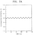
- FIGS. 2A and 2B are graphs showing piezoelectric potentials of a nano-piezoelectric generator according to a comparative example.
- the nano-piezoelectric generator according to the comparative example does not include an interlayer.
- FIG. 2A shows a case in which ITO is used to form an electrode
- FIG. 2B shows a case in which Pt or Au is used to form an electrode.
- a piezoelectric potential when ITO is used to form an electrode is lower than that when Pt or Au, that is, a metal material, is used to form an electrode.
- Pt which has a high work function
- a piezoelectric potential is higher than that when Au is used to form an electrode. From the graphs, there is a limitation in selecting an electrode material for improving a piezoelectric efficiency.
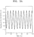
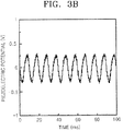
- FIGS. 3A and 3B are graphs showing piezoelectric potentials of the nano-piezoelectric generator 100 shown in FIG. 1 , wherein FIG. 3A shows a case where the interlayer 130 is formed of MoO 3 and FIG. 3B shows a case where the interlayer 130 is formed of VO 2 .
- the graphs of FIGS. 3A and 3B show piezoelectric potentials when an electrode is formed of ITO.
- a piezoelectric potential is much higher than that of FIG. 2A where an interlayer is not formed and an electrode is formed of ITO, that is, the piezoelectric potential is about 20 times higher than that of FIG. 2A .
- the piezoelectric potential is at least twice as great.
- a piezoelectric potential is improved when the interlayer 130 is formed of VO 2 .
- FIG. 4 is a perspective view of a nano-piezoelectric generator 200 according to another exemplary embodiment.
- the nano-piezoelectric generator 200 of the present embodiment is different from the nano-piezoelectric generator 100 of FIG. 1 with respect to the structure of a nano-piezoelectric units 240.
- Each nano-piezoelectric unit 240 includes a nano-structure including a predetermined first carrier therein, and a density adjusting unit for adjusting a density of the first carrier.
- the density adjusting unit may be a second carrier having a polarity opposite to that of the first carrier and doped in the nano-structure.
- the first carrier may be an n-type carrier and the second carrier may be a p-type carrier, and Li may be used as the p-type carrier.
- the above structure is derived from a characteristic that a piezoelectric efficiency is improved as a carrier density in a nano-structure is lowered, and thus the density of the first carrier in the nano-structure of the nano-piezoelectric unit 240 is controlled and the interlayer 130 is formed in the nano-piezoelectric generator 200 in order to realize a high piezoelectric efficiency.
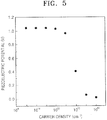
- FIG. 5 is a computer simulation graph showing a piezoelectric potential with respect to a carrier density in a ZnO nano-wire.
- the ZnO nano-wire is modeled as a hexagonal prism having a diameter of 200 nm and a length of 600 nm.
- a diameter is a length of the longest diagonal line of a hexagon base of the hexagonal prism.
- a bottom surface of the ZnO nano-wire is bonded to a substrate and electrically grounded, and an external stress (Tz) of 10 7 N/m 2 is applied from a top surface of the ZnO nano-wire along a length direction of the nano-wire.
- An induced piezoelectric potential is calculated as a function of density at a center of the top surface of the ZnO nano-wire. Referring to the graph of FIG. 5 , when the carrier density is increased, the piezoelectric potential is lowered. In addition, when the carrier density is greater than about 10 15 /cm 3 , the piezoelectric potential is sharply lowered.
- FIGS. 6A through 6C are diagrams showing other examples of the nano-piezoelectric unit 240 that may be included in the nano-piezoelectric generator 200 of FIG. 4 .
- the nano-piezoelectric unit 240 includes a nano-structure 241 including a predetermined first carrier therein and a functional group attached on a surface of the nano-structure 241.
- the functional group has electric charges of the same polarity as that of the first carrier, for example, the nano-structure 241 may be formed of the ZnO semiconductor nano-wire, and as shown in the drawings, the functional group may be a carboxyl group of negative charges.
- FIG. 7 is a diagram showing another example of the nano-piezoelectric unit 240 that may be included in the nano-piezoelectric generator 200 of FIG. 4 .
- the nano-piezoelectric unit 240 includes the nano-structure 241 including a predetermined first carrier and a ferroelectric substance 245 applied on a surface of the nano-structure 241.
- the ferroelectric substance 245 coated on the surface of the nano-structure 241 aligns an electric dipole 247 in a direction to control a density of an internal carrier.
- FIG. 7 when the ferroelectric substance 245 applies a positive voltage to the nano-structure 241 of a nano-wire shape, negative charges are concentrated on a side of the ferroelectric substance 245 relatively close to the nano-wire and positive charges are concentrated on a side of the ferroelectric substance 245 relatively far from the nano-wire.
- the ferroelectric substance 245 may be formed of PVDF, BTO, or PZT.
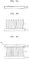
- FIGS. 8A through 8C are diagrams illustrating a method of manufacturing a nano-piezoelectric generator 300 according to an exemplary embodiment.
- a first electrode 320 is prepared, and an interlayer 330, formed of an insulating material, is formed on the first electrode 320.
- the first electrode 320 may be formed on a substrate (not shown).
- the first electrode 320 may be formed of a metal material, a conductive oxide, or a conductive polymer.
- the interlayer 330 may be formed of an oxide material, a polymer, or a combination thereof.
- the interlayer 330 may be formed in various ways according to the material forming the interlayer 330, for example, sol-gel synthesis, thermal evaporation, electron beam evaporation, sputtering, laser ablation, or spin coating.
- nano-piezoelectric units 340 are formed on a second substrate 350.
- the nano-piezoelectric units 340 may be formed of GaN or ZnO, and may be formed as nanorods, nano-pores, or nano-tubes, or formed to have nano-wire shapes, as shown in FIG. 8B .
- the nano-piezoelectric unit 340 may include a nano-structure including a first carrier therein and a density adjusting unit for adjusting a density of the first carrier, as described with reference to FIG. 4 .
- the nano-piezoelectric units 340 and the interlayer 330 are bonded to each other to manufacture the nano-piezoelectric generator 300.
- an entire structure may be fixed by using an epoxy; however, exemplary embodiments are not limited thereto.
- a nano-piezoelectric generator may include an interlayer formed of an insulating material is inserted between an electrode and a piezoelectric material so as to increase a selection range of electrode materials and to improve a piezoelectric efficiency.
- a structure for adjusting a carrier density in a nano-structure may be formed, thereby further improving the piezoelectric efficiency.
Landscapes
- Engineering & Computer Science (AREA)
- Manufacturing & Machinery (AREA)
- Chemical & Material Sciences (AREA)
- Ceramic Engineering (AREA)
- General Electrical Machinery Utilizing Piezoelectricity, Electrostriction Or Magnetostriction (AREA)
Claims (15)
- Nanopiezoelektrischer Generator, Folgendes umfassend:eine erste Elektrode (120) und eine zweite Elektrode (150);zumindest eine nanopiezoelektrische Einheit (140, 240), die eine Nanostruktur umfasst, die von einem piezoelektrischen Halbleitermaterial ausgebildet wird, die zwischen der ersten Elektrode (120) und der zweiten Elektrode (150) angeordnet ist; undeine Zwischenschicht (130), die von einem Isoliermaterial ausgebildet wird, die zwischen der ersten Elektrode und der zumindest einen nanopiezoelektrischen Einheit angeordnet ist;dadurch gekennzeichnet, dass die Zwischenschicht ein Oxid umfasst.
- Nanopiezoelektrischer Generator nach Anspruch 1, wobei die Zwischenschicht eines von WO3, HfO2, Al2O3, ZrO2, Si3N4, Ta2O5, MgO, Y2O3, La2O3, SiO2, MoO3 und VO2 umfasst.
- Nanopiezoelektrischer Generator nach einem der vorhergehenden Ansprüche, wobei die nanopiezoelektrische Einheit ZnO und GaN umfasst.
- Nanopiezoelektrischer Generator nach einem der vorhergehenden Ansprüche, wobei die nanopiezoelektrische Einheit (140, 240) Folgendes umfasst:eine Nanostruktur, die einen ersten Träger umfasst; undeine Dichteregulierungseinheit, die die Regulierung einer Dichte des ersten Trägers ermöglicht.
- Nanopiezoelektrischer Generator nach Anspruch 4, wobei die Dichteregulierungseinheit einen zweiten Träger umfasst, der in der Nanostruktur dotiert ist und eine der Polarität des ersten Trägers entgegengesetzte Polarität aufweist.
- Nanopiezoelektrischer Generator nach Anspruch 5, wobei die Nanostruktur ein ZnO-Halbleiter-Nanodraht ist und der zweite Träger p-Typ-Verunreinigungen aufweist, wobei bevorzugt die p-Typ-Verunreinigungen Li sind.
- Nanopiezoelektrischer Generator nach Anspruch 4, wobei die Dichteregulierungseinheit eine Funktionsgruppe umfasst, die an einer Oberfläche der Nanostruktur angebracht ist, und wobei eine Polarität der Funktionsgruppe einer Polarität des ersten Trägers entspricht, und wobei bevorzugt die Nanostruktur ein ZnO-Halbleiter-Nanodraht ist und die Funktionsgruppe negative Ladungen aufweist.
- Nanopiezoelektrischer Generator nach Anspruch 4, wobei die Dichteregulierungseinheit ein ferroelektrisches Material umfasst, mit dem eine Oberfläche der Nanostruktur beschichtet ist.
- Verfahren zur Herstellung eines nanopiezoelektrischen Generators, wobei das Verfahren Folgendes umfasst:Ausbilden einer Zwischenschicht (130), die ein Isoliermaterial umfasst, auf einer ersten Elektrode (120);Ausbilden zumindest einer nanopiezoelektrischen Einheit (140, 240), die eine Nanostruktur, die von einem piezoelektrischen Halbleitermaterial ausgebildet wird, auf einer zweiten Elektrode (150) umfasst; und Verbinden der zumindest einen nanopiezoelektrischen Einheit (140, 240) mit der Zwischenschicht (130), dadurch gekennzeichnet, dass die Zwischenschicht ein Oxid umfasst.
- Verfahren nach Anspruch 9, wobei die Zwischenschicht eines von WO3, HfO2, Al2O3, ZrO2, Si3N4, Ta2O5, MgO, Y2O3, La2O3, SiO2, MoO3 und VO2 umfasst.
- Verfahren nach Anspruch 9 oder 10, wobei die erste Elektrode ein Metallmaterial, ein leitfähiges Oxid und ein leitfähiges Polymer umfasst und wobei bevorzugt die nanopiezoelektrische Einheit eines von ZnO und GaN umfasst.
- Verfahren nach Anspruch 10, wobei das Ausbilden der zumindest einen nanopiezoelektrischen Einheit (140, 240) Folgendes umfasst:Ausbilden einer Nanostruktur, die einen ersten Träger in der Nanostruktur umfasst; undRegulieren einer Dichte des ersten Trägers.
- Verfahren nach Anspruch 12, wobei das Regulieren der Dichte des ersten Trägers das Dotieren eines zweiten Trägers umfasst, wenn die Nanostruktur ausgebildet wird, wobei eine Polarität des zweiten Trägers einer Polarität des ersten Trägers entgegengesetzt ist.
- Verfahren nach Anspruch 12, wobei das Regulieren der Dichte des ersten Trägers das Anbringen einer Funktionsgruppe an einer Oberfläche der Nanostruktur umfasst, wobei eine Polarität der Funktionsgruppe einer Polarität des ersten Trägers entspricht.
- Verfahren nach Anspruch 12, wobei das Regulieren der Dichte des ersten Trägers das Beschichten eines ferroelektrischen Materials auf einer Oberfläche der Nanostruktur umfasst.
Applications Claiming Priority (1)
| Application Number | Priority Date | Filing Date | Title |
|---|---|---|---|
| KR1020120018655A KR101861148B1 (ko) | 2012-02-23 | 2012-02-23 | 나노 압전 발전 소자 및 그 제조방법 |
Publications (3)
| Publication Number | Publication Date |
|---|---|
| EP2631960A2 EP2631960A2 (de) | 2013-08-28 |
| EP2631960A3 EP2631960A3 (de) | 2014-09-17 |
| EP2631960B1 true EP2631960B1 (de) | 2016-04-06 |
Family
ID=47709839
Family Applications (1)
| Application Number | Title | Priority Date | Filing Date |
|---|---|---|---|
| EP13151703.9A Active EP2631960B1 (de) | 2012-02-23 | 2013-01-17 | Nanopiezoelektrischer Generator und Herstellungsverfahren dafür |
Country Status (4)
| Country | Link |
|---|---|
| US (1) | US9312468B2 (de) |
| EP (1) | EP2631960B1 (de) |
| KR (1) | KR101861148B1 (de) |
| CN (1) | CN103296922B (de) |
Families Citing this family (15)
| Publication number | Priority date | Publication date | Assignee | Title |
|---|---|---|---|---|
| US9059397B2 (en) * | 2008-12-08 | 2015-06-16 | Electronics And Telecommunications Research Institute | Nano piezoelectric device having a nanowire and method of forming the same |
| US20140174496A1 (en) | 2012-12-21 | 2014-06-26 | Georgia Tech Research Corporation | Hybrid generator using thermoelectric generation and piezoelectric generation |
| KR101720166B1 (ko) * | 2015-03-31 | 2017-03-28 | 한국과학기술원 | 압전 나노 자가발전 소자 및 그 제조 방법 |
| CN104976685A (zh) * | 2015-06-07 | 2015-10-14 | 深圳市沃森空调技术有限公司 | 声音驱动空调室内机 |
| CN105552211A (zh) * | 2016-01-18 | 2016-05-04 | 辽宁广告职业学院 | 一种声控挤压式发电薄膜及其制备方法 |
| CN107275475B (zh) * | 2017-07-11 | 2019-07-05 | 中南大学 | 一种TiO2@PZT纳米线阵列/聚合物的复合介电材料及其制备方法 |
| JP6941398B2 (ja) * | 2017-08-04 | 2021-09-29 | コリア ポリテクニック ユニバーシティ インダストリー アカデミック コーオペレイション ファウンデーションKorea Polytechnic University Industry Academic Cooperation Foundation | ナノロッド構造を用いた超音波指紋センサーの製造方法 |
| US11031657B2 (en) | 2017-11-28 | 2021-06-08 | Massachusetts Institute Of Technology | Separators comprising elongated nanostructures and associated devices and methods, including devices and methods for energy storage and/or use |
| US11594574B2 (en) | 2018-02-16 | 2023-02-28 | International Business Machines Corporation | Piezo-junction device |
| CN109585642A (zh) * | 2018-11-06 | 2019-04-05 | 浙江海洋大学 | 一种基于pet/银纳米线/氧化锌镁/氧化锌镁纳米阵列的纳米发电机 |
| KR102472120B1 (ko) * | 2019-05-03 | 2022-11-28 | 메이 선 테크놀로지 씨오 엘티디 | 의사-압전 d33 진동 장치 및 이를 통합하는 디스플레이 |
| US11545612B2 (en) | 2019-05-03 | 2023-01-03 | May Sun Technology Co., Ltd. | Pseudo-piezoelectric D33 device and electronic device using the same |
| CN110739880B (zh) * | 2019-10-28 | 2021-04-02 | 北京科技大学 | 一种碳化硅纳米线阵列基压电纳米发电机的制备方法 |
| TWI771064B (zh) * | 2021-06-16 | 2022-07-11 | 美三科技有限公司 | 類壓電d33裝置及使用其的電子設備 |
| KR102777802B1 (ko) * | 2023-04-13 | 2025-03-06 | 충남대학교산학협력단 | 압전소자 및 압전소자의 제작방법 |
Family Cites Families (19)
| Publication number | Priority date | Publication date | Assignee | Title |
|---|---|---|---|---|
| US7135728B2 (en) * | 2002-09-30 | 2006-11-14 | Nanosys, Inc. | Large-area nanoenabled macroelectronic substrates and uses therefor |
| TWI232944B (en) * | 2003-10-17 | 2005-05-21 | Ind Tech Res Inst | MEMS differential actuated scanning nano probe |
| US7408147B2 (en) * | 2005-07-27 | 2008-08-05 | Wisconsin Alumni Research Foundation | Nanoelectromechanical and microelectromechanical sensors and analyzers |
| US8330154B2 (en) | 2005-12-20 | 2012-12-11 | Georgia Tech Research Corporation | Piezoelectric and semiconducting coupled nanogenerators |
| US8039834B2 (en) | 2006-06-13 | 2011-10-18 | Georgia Tech Research Corporation | Nanogenerator comprising piezoelectric semiconducting nanostructures and Schottky conductive contacts |
| US20110275947A1 (en) * | 2007-01-04 | 2011-11-10 | Board Of Regents, The University Of Texas System | Cardiovascular power source for automatic implantable cardioverter defibrillators |
| US7705523B2 (en) | 2008-05-27 | 2010-04-27 | Georgia Tech Research Corporation | Hybrid solar nanogenerator cells |
| KR101454686B1 (ko) | 2008-09-17 | 2014-10-28 | 삼성전자주식회사 | 에너지 변환 장치 및 방법 |
| US9059397B2 (en) * | 2008-12-08 | 2015-06-16 | Electronics And Telecommunications Research Institute | Nano piezoelectric device having a nanowire and method of forming the same |
| KR101562060B1 (ko) * | 2009-04-06 | 2015-10-21 | 삼성전자주식회사 | 전기 에너지 발생 장치 및 그 제조 방법 |
| KR20110047860A (ko) * | 2009-10-30 | 2011-05-09 | 삼성전자주식회사 | 압전 나노와이어 구조체 및 이를 포함하는 전기 기기 |
| CN101860261B (zh) * | 2010-03-26 | 2012-11-28 | 辽宁师范大学 | 一种逆压电纳米半导体发电机 |
| US8367462B2 (en) * | 2010-04-21 | 2013-02-05 | Georgia Tech Research Corporation | Large-scale fabrication of vertically aligned ZnO nanowire arrays |
| US8901247B2 (en) * | 2010-05-28 | 2014-12-02 | The Regents Of The University Of California | Responsive polymer system and nanohybrid thin films |
| KR20110135293A (ko) | 2010-06-10 | 2011-12-16 | 삼성전자주식회사 | p형 Zn 산화물 나노 와이어의 제조 방법 및 p형 Zn 산화물을 포함하는 전자 소자 |
| KR101713280B1 (ko) | 2011-03-03 | 2017-03-08 | 삼성전자주식회사 | 전기 에너지 발생장치 |
| KR101781551B1 (ko) | 2011-07-20 | 2017-09-27 | 삼성전자주식회사 | 전기에너지 발생 소자 및 그 구동방법 |
| CN102299252B (zh) * | 2011-08-31 | 2013-08-21 | 中国人民解放军国防科学技术大学 | 异质结压电式纳米发电机及其制造方法 |
| KR101878350B1 (ko) | 2012-01-10 | 2018-08-08 | 삼성전자주식회사 | 나노 압전 발전 소자 및 그 제조방법 |
-
2012
- 2012-02-23 KR KR1020120018655A patent/KR101861148B1/ko not_active Expired - Fee Related
- 2012-12-25 CN CN201210570140.3A patent/CN103296922B/zh active Active
-
2013
- 2013-01-17 EP EP13151703.9A patent/EP2631960B1/de active Active
- 2013-02-22 US US13/774,039 patent/US9312468B2/en active Active
Also Published As
| Publication number | Publication date |
|---|---|
| US9312468B2 (en) | 2016-04-12 |
| EP2631960A2 (de) | 2013-08-28 |
| CN103296922B (zh) | 2017-03-01 |
| CN103296922A (zh) | 2013-09-11 |
| EP2631960A3 (de) | 2014-09-17 |
| KR101861148B1 (ko) | 2018-05-25 |
| KR20130096992A (ko) | 2013-09-02 |
| US20130221806A1 (en) | 2013-08-29 |
Similar Documents
| Publication | Publication Date | Title |
|---|---|---|
| EP2631960B1 (de) | Nanopiezoelektrischer Generator und Herstellungsverfahren dafür | |
| KR101878350B1 (ko) | 나노 압전 발전 소자 및 그 제조방법 | |
| EP2290718B1 (de) | Vorrichtung zur Erzeugung elektrischer Energie und Herstellungsverfahren dafür | |
| Li et al. | Recent progress on piezoelectric energy harvesting: structures and materials | |
| US9287487B2 (en) | Textile-based stretchable energy generator | |
| Zhu et al. | Flexible high-output nanogenerator based on lateral ZnO nanowire array | |
| KR101769459B1 (ko) | 나노 발전 소자 및 그 제조 방법 | |
| US8785914B2 (en) | Piezoelectric nanowire structure and electronic device including the same | |
| KR101647034B1 (ko) | 전기 에너지 발생 장치 및 그 제조 방법 | |
| KR102051518B1 (ko) | 자가 동력 터치 센서 겸용 에너지 수확 장치 | |
| KR102703712B1 (ko) | 마찰전기 발전기 | |
| KR20110095659A (ko) | 전기 에너지 발생 장치 | |
| KR101809376B1 (ko) | 압전 하베스팅 소자 | |
| KR101982280B1 (ko) | 적층된 구조를 가지는 직물 기반의 에너지 제너레이터 | |
| KR101796176B1 (ko) | 압전 나노와이어 구조체 및 이를 포함하는 전기 기기 | |
| Hannachi et al. | Nanomaterials for nanogenerator | |
| KR20180020329A (ko) | 압전 하베스팅 소자 |
Legal Events
| Date | Code | Title | Description |
|---|---|---|---|
| PUAI | Public reference made under article 153(3) epc to a published international application that has entered the european phase |
Free format text: ORIGINAL CODE: 0009012 |
|
| AK | Designated contracting states |
Kind code of ref document: A2 Designated state(s): AL AT BE BG CH CY CZ DE DK EE ES FI FR GB GR HR HU IE IS IT LI LT LU LV MC MK MT NL NO PL PT RO RS SE SI SK SM TR |
|
| AX | Request for extension of the european patent |
Extension state: BA ME |
|
| PUAL | Search report despatched |
Free format text: ORIGINAL CODE: 0009013 |
|
| AK | Designated contracting states |
Kind code of ref document: A3 Designated state(s): AL AT BE BG CH CY CZ DE DK EE ES FI FR GB GR HR HU IE IS IT LI LT LU LV MC MK MT NL NO PL PT RO RS SE SI SK SM TR |
|
| AX | Request for extension of the european patent |
Extension state: BA ME |
|
| RIC1 | Information provided on ipc code assigned before grant |
Ipc: H02N 2/18 20060101ALI20140813BHEP Ipc: H01L 41/39 20130101AFI20140813BHEP Ipc: H01L 41/113 20060101ALI20140813BHEP Ipc: H01L 41/18 20060101ALI20140813BHEP |
|
| 17P | Request for examination filed |
Effective date: 20150317 |
|
| RBV | Designated contracting states (corrected) |
Designated state(s): AL AT BE BG CH CY CZ DE DK EE ES FI FR GB GR HR HU IE IS IT LI LT LU LV MC MK MT NL NO PL PT RO RS SE SI SK SM TR |
|
| GRAP | Despatch of communication of intention to grant a patent |
Free format text: ORIGINAL CODE: EPIDOSNIGR1 |
|
| RIC1 | Information provided on ipc code assigned before grant |
Ipc: H01L 41/18 20060101ALI20150825BHEP Ipc: H02N 2/18 20060101ALI20150825BHEP Ipc: H01L 41/22 20130101ALI20150825BHEP Ipc: H01L 41/113 20060101ALI20150825BHEP Ipc: H01L 41/39 20130101AFI20150825BHEP |
|
| INTG | Intention to grant announced |
Effective date: 20150921 |
|
| RAP1 | Party data changed (applicant data changed or rights of an application transferred) |
Owner name: SAMSUNG ELECTRONICS CO., LTD. |
|
| GRAS | Grant fee paid |
Free format text: ORIGINAL CODE: EPIDOSNIGR3 |
|
| GRAA | (expected) grant |
Free format text: ORIGINAL CODE: 0009210 |
|
| AK | Designated contracting states |
Kind code of ref document: B1 Designated state(s): AL AT BE BG CH CY CZ DE DK EE ES FI FR GB GR HR HU IE IS IT LI LT LU LV MC MK MT NL NO PL PT RO RS SE SI SK SM TR |
|
| REG | Reference to a national code |
Ref country code: GB Ref legal event code: FG4D |
|
| REG | Reference to a national code |
Ref country code: AT Ref legal event code: REF Ref document number: 788625 Country of ref document: AT Kind code of ref document: T Effective date: 20160415 Ref country code: CH Ref legal event code: EP |
|
| REG | Reference to a national code |
Ref country code: IE Ref legal event code: FG4D |
|
| REG | Reference to a national code |
Ref country code: DE Ref legal event code: R096 Ref document number: 602013006062 Country of ref document: DE |
|
| REG | Reference to a national code |
Ref country code: LT Ref legal event code: MG4D Ref country code: NL Ref legal event code: MP Effective date: 20160406 |
|
| REG | Reference to a national code |
Ref country code: AT Ref legal event code: MK05 Ref document number: 788625 Country of ref document: AT Kind code of ref document: T Effective date: 20160406 |
|
| PG25 | Lapsed in a contracting state [announced via postgrant information from national office to epo] |
Ref country code: NL Free format text: LAPSE BECAUSE OF FAILURE TO SUBMIT A TRANSLATION OF THE DESCRIPTION OR TO PAY THE FEE WITHIN THE PRESCRIBED TIME-LIMIT Effective date: 20160406 |
|
| PG25 | Lapsed in a contracting state [announced via postgrant information from national office to epo] |
Ref country code: LT Free format text: LAPSE BECAUSE OF FAILURE TO SUBMIT A TRANSLATION OF THE DESCRIPTION OR TO PAY THE FEE WITHIN THE PRESCRIBED TIME-LIMIT Effective date: 20160406 Ref country code: PL Free format text: LAPSE BECAUSE OF FAILURE TO SUBMIT A TRANSLATION OF THE DESCRIPTION OR TO PAY THE FEE WITHIN THE PRESCRIBED TIME-LIMIT Effective date: 20160406 Ref country code: NO Free format text: LAPSE BECAUSE OF FAILURE TO SUBMIT A TRANSLATION OF THE DESCRIPTION OR TO PAY THE FEE WITHIN THE PRESCRIBED TIME-LIMIT Effective date: 20160706 Ref country code: IS Free format text: LAPSE BECAUSE OF FAILURE TO SUBMIT A TRANSLATION OF THE DESCRIPTION OR TO PAY THE FEE WITHIN THE PRESCRIBED TIME-LIMIT Effective date: 20160806 Ref country code: FI Free format text: LAPSE BECAUSE OF FAILURE TO SUBMIT A TRANSLATION OF THE DESCRIPTION OR TO PAY THE FEE WITHIN THE PRESCRIBED TIME-LIMIT Effective date: 20160406 |
|
| PG25 | Lapsed in a contracting state [announced via postgrant information from national office to epo] |
Ref country code: GR Free format text: LAPSE BECAUSE OF FAILURE TO SUBMIT A TRANSLATION OF THE DESCRIPTION OR TO PAY THE FEE WITHIN THE PRESCRIBED TIME-LIMIT Effective date: 20160707 Ref country code: PT Free format text: LAPSE BECAUSE OF FAILURE TO SUBMIT A TRANSLATION OF THE DESCRIPTION OR TO PAY THE FEE WITHIN THE PRESCRIBED TIME-LIMIT Effective date: 20160808 Ref country code: SE Free format text: LAPSE BECAUSE OF FAILURE TO SUBMIT A TRANSLATION OF THE DESCRIPTION OR TO PAY THE FEE WITHIN THE PRESCRIBED TIME-LIMIT Effective date: 20160406 Ref country code: HR Free format text: LAPSE BECAUSE OF FAILURE TO SUBMIT A TRANSLATION OF THE DESCRIPTION OR TO PAY THE FEE WITHIN THE PRESCRIBED TIME-LIMIT Effective date: 20160406 Ref country code: AT Free format text: LAPSE BECAUSE OF FAILURE TO SUBMIT A TRANSLATION OF THE DESCRIPTION OR TO PAY THE FEE WITHIN THE PRESCRIBED TIME-LIMIT Effective date: 20160406 Ref country code: RS Free format text: LAPSE BECAUSE OF FAILURE TO SUBMIT A TRANSLATION OF THE DESCRIPTION OR TO PAY THE FEE WITHIN THE PRESCRIBED TIME-LIMIT Effective date: 20160406 Ref country code: LV Free format text: LAPSE BECAUSE OF FAILURE TO SUBMIT A TRANSLATION OF THE DESCRIPTION OR TO PAY THE FEE WITHIN THE PRESCRIBED TIME-LIMIT Effective date: 20160406 Ref country code: ES Free format text: LAPSE BECAUSE OF FAILURE TO SUBMIT A TRANSLATION OF THE DESCRIPTION OR TO PAY THE FEE WITHIN THE PRESCRIBED TIME-LIMIT Effective date: 20160406 |
|
| REG | Reference to a national code |
Ref country code: FR Ref legal event code: PLFP Year of fee payment: 5 |
|
| PG25 | Lapsed in a contracting state [announced via postgrant information from national office to epo] |
Ref country code: BE Free format text: LAPSE BECAUSE OF FAILURE TO SUBMIT A TRANSLATION OF THE DESCRIPTION OR TO PAY THE FEE WITHIN THE PRESCRIBED TIME-LIMIT Effective date: 20160406 Ref country code: IT Free format text: LAPSE BECAUSE OF FAILURE TO SUBMIT A TRANSLATION OF THE DESCRIPTION OR TO PAY THE FEE WITHIN THE PRESCRIBED TIME-LIMIT Effective date: 20160406 |
|
| REG | Reference to a national code |
Ref country code: DE Ref legal event code: R097 Ref document number: 602013006062 Country of ref document: DE |
|
| PG25 | Lapsed in a contracting state [announced via postgrant information from national office to epo] |
Ref country code: CZ Free format text: LAPSE BECAUSE OF FAILURE TO SUBMIT A TRANSLATION OF THE DESCRIPTION OR TO PAY THE FEE WITHIN THE PRESCRIBED TIME-LIMIT Effective date: 20160406 Ref country code: SK Free format text: LAPSE BECAUSE OF FAILURE TO SUBMIT A TRANSLATION OF THE DESCRIPTION OR TO PAY THE FEE WITHIN THE PRESCRIBED TIME-LIMIT Effective date: 20160406 Ref country code: EE Free format text: LAPSE BECAUSE OF FAILURE TO SUBMIT A TRANSLATION OF THE DESCRIPTION OR TO PAY THE FEE WITHIN THE PRESCRIBED TIME-LIMIT Effective date: 20160406 Ref country code: RO Free format text: LAPSE BECAUSE OF FAILURE TO SUBMIT A TRANSLATION OF THE DESCRIPTION OR TO PAY THE FEE WITHIN THE PRESCRIBED TIME-LIMIT Effective date: 20160406 Ref country code: DK Free format text: LAPSE BECAUSE OF FAILURE TO SUBMIT A TRANSLATION OF THE DESCRIPTION OR TO PAY THE FEE WITHIN THE PRESCRIBED TIME-LIMIT Effective date: 20160406 |
|
| PLBE | No opposition filed within time limit |
Free format text: ORIGINAL CODE: 0009261 |
|
| STAA | Information on the status of an ep patent application or granted ep patent |
Free format text: STATUS: NO OPPOSITION FILED WITHIN TIME LIMIT |
|
| PG25 | Lapsed in a contracting state [announced via postgrant information from national office to epo] |
Ref country code: SM Free format text: LAPSE BECAUSE OF FAILURE TO SUBMIT A TRANSLATION OF THE DESCRIPTION OR TO PAY THE FEE WITHIN THE PRESCRIBED TIME-LIMIT Effective date: 20160406 |
|
| 26N | No opposition filed |
Effective date: 20170110 |
|
| PG25 | Lapsed in a contracting state [announced via postgrant information from national office to epo] |
Ref country code: SI Free format text: LAPSE BECAUSE OF FAILURE TO SUBMIT A TRANSLATION OF THE DESCRIPTION OR TO PAY THE FEE WITHIN THE PRESCRIBED TIME-LIMIT Effective date: 20160406 |
|
| REG | Reference to a national code |
Ref country code: CH Ref legal event code: PL |
|
| PG25 | Lapsed in a contracting state [announced via postgrant information from national office to epo] |
Ref country code: MC Free format text: LAPSE BECAUSE OF FAILURE TO SUBMIT A TRANSLATION OF THE DESCRIPTION OR TO PAY THE FEE WITHIN THE PRESCRIBED TIME-LIMIT Effective date: 20160406 |
|
| PG25 | Lapsed in a contracting state [announced via postgrant information from national office to epo] |
Ref country code: LI Free format text: LAPSE BECAUSE OF NON-PAYMENT OF DUE FEES Effective date: 20170131 Ref country code: CH Free format text: LAPSE BECAUSE OF NON-PAYMENT OF DUE FEES Effective date: 20170131 |
|
| REG | Reference to a national code |
Ref country code: IE Ref legal event code: MM4A |
|
| PG25 | Lapsed in a contracting state [announced via postgrant information from national office to epo] |
Ref country code: LU Free format text: LAPSE BECAUSE OF NON-PAYMENT OF DUE FEES Effective date: 20170117 |
|
| REG | Reference to a national code |
Ref country code: FR Ref legal event code: PLFP Year of fee payment: 6 |
|
| PG25 | Lapsed in a contracting state [announced via postgrant information from national office to epo] |
Ref country code: IE Free format text: LAPSE BECAUSE OF NON-PAYMENT OF DUE FEES Effective date: 20170117 |
|
| PG25 | Lapsed in a contracting state [announced via postgrant information from national office to epo] |
Ref country code: MT Free format text: LAPSE BECAUSE OF NON-PAYMENT OF DUE FEES Effective date: 20170117 |
|
| PG25 | Lapsed in a contracting state [announced via postgrant information from national office to epo] |
Ref country code: AL Free format text: LAPSE BECAUSE OF FAILURE TO SUBMIT A TRANSLATION OF THE DESCRIPTION OR TO PAY THE FEE WITHIN THE PRESCRIBED TIME-LIMIT Effective date: 20160406 |
|
| PG25 | Lapsed in a contracting state [announced via postgrant information from national office to epo] |
Ref country code: HU Free format text: LAPSE BECAUSE OF FAILURE TO SUBMIT A TRANSLATION OF THE DESCRIPTION OR TO PAY THE FEE WITHIN THE PRESCRIBED TIME-LIMIT; INVALID AB INITIO Effective date: 20130117 |
|
| PG25 | Lapsed in a contracting state [announced via postgrant information from national office to epo] |
Ref country code: BG Free format text: LAPSE BECAUSE OF FAILURE TO SUBMIT A TRANSLATION OF THE DESCRIPTION OR TO PAY THE FEE WITHIN THE PRESCRIBED TIME-LIMIT Effective date: 20160406 |
|
| PG25 | Lapsed in a contracting state [announced via postgrant information from national office to epo] |
Ref country code: CY Free format text: LAPSE BECAUSE OF NON-PAYMENT OF DUE FEES Effective date: 20160406 |
|
| PG25 | Lapsed in a contracting state [announced via postgrant information from national office to epo] |
Ref country code: MK Free format text: LAPSE BECAUSE OF FAILURE TO SUBMIT A TRANSLATION OF THE DESCRIPTION OR TO PAY THE FEE WITHIN THE PRESCRIBED TIME-LIMIT Effective date: 20160406 |
|
| PG25 | Lapsed in a contracting state [announced via postgrant information from national office to epo] |
Ref country code: TR Free format text: LAPSE BECAUSE OF FAILURE TO SUBMIT A TRANSLATION OF THE DESCRIPTION OR TO PAY THE FEE WITHIN THE PRESCRIBED TIME-LIMIT Effective date: 20160406 |
|
| REG | Reference to a national code |
Ref country code: DE Ref legal event code: R079 Ref document number: 602013006062 Country of ref document: DE Free format text: PREVIOUS MAIN CLASS: H01L0041390000 Ipc: H10N0030093000 |
|
| P01 | Opt-out of the competence of the unified patent court (upc) registered |
Effective date: 20230530 |
|
| PGFP | Annual fee paid to national office [announced via postgrant information from national office to epo] |
Ref country code: GB Payment date: 20251211 Year of fee payment: 14 |
|
| PGFP | Annual fee paid to national office [announced via postgrant information from national office to epo] |
Ref country code: FR Payment date: 20251222 Year of fee payment: 14 |
|
| PGFP | Annual fee paid to national office [announced via postgrant information from national office to epo] |
Ref country code: DE Payment date: 20251216 Year of fee payment: 14 |