EP2631750A2 - Geteilte Abfrageleitungen für negativen Pixelausgleich - Google Patents
Geteilte Abfrageleitungen für negativen Pixelausgleich Download PDFInfo
- Publication number
- EP2631750A2 EP2631750A2 EP13156753.9A EP13156753A EP2631750A2 EP 2631750 A2 EP2631750 A2 EP 2631750A2 EP 13156753 A EP13156753 A EP 13156753A EP 2631750 A2 EP2631750 A2 EP 2631750A2
- Authority
- EP
- European Patent Office
- Prior art keywords
- panel
- capacitance
- strips
- sense
- touch
- Prior art date
- Legal status (The legal status is an assumption and is not a legal conclusion. Google has not performed a legal analysis and makes no representation as to the accuracy of the status listed.)
- Ceased
Links
Images



Classifications
-
- G—PHYSICS
- G06—COMPUTING OR CALCULATING; COUNTING
- G06F—ELECTRIC DIGITAL DATA PROCESSING
- G06F3/00—Input arrangements for transferring data to be processed into a form capable of being handled by the computer; Output arrangements for transferring data from processing unit to output unit, e.g. interface arrangements
- G06F3/01—Input arrangements or combined input and output arrangements for interaction between user and computer
- G06F3/03—Arrangements for converting the position or the displacement of a member into a coded form
- G06F3/041—Digitisers, e.g. for touch screens or touch pads, characterised by the transducing means
- G06F3/044—Digitisers, e.g. for touch screens or touch pads, characterised by the transducing means by capacitive means
-
- G—PHYSICS
- G06—COMPUTING OR CALCULATING; COUNTING
- G06F—ELECTRIC DIGITAL DATA PROCESSING
- G06F3/00—Input arrangements for transferring data to be processed into a form capable of being handled by the computer; Output arrangements for transferring data from processing unit to output unit, e.g. interface arrangements
- G06F3/01—Input arrangements or combined input and output arrangements for interaction between user and computer
- G06F3/03—Arrangements for converting the position or the displacement of a member into a coded form
- G06F3/041—Digitisers, e.g. for touch screens or touch pads, characterised by the transducing means
- G06F3/0416—Control or interface arrangements specially adapted for digitisers
- G06F3/04166—Details of scanning methods, e.g. sampling time, grouping of sub areas or time sharing with display driving
-
- G—PHYSICS
- G06—COMPUTING OR CALCULATING; COUNTING
- G06F—ELECTRIC DIGITAL DATA PROCESSING
- G06F3/00—Input arrangements for transferring data to be processed into a form capable of being handled by the computer; Output arrangements for transferring data from processing unit to output unit, e.g. interface arrangements
- G06F3/01—Input arrangements or combined input and output arrangements for interaction between user and computer
- G06F3/03—Arrangements for converting the position or the displacement of a member into a coded form
- G06F3/041—Digitisers, e.g. for touch screens or touch pads, characterised by the transducing means
- G06F3/0416—Control or interface arrangements specially adapted for digitisers
- G06F3/0418—Control or interface arrangements specially adapted for digitisers for error correction or compensation, e.g. based on parallax, calibration or alignment
-
- G—PHYSICS
- G06—COMPUTING OR CALCULATING; COUNTING
- G06F—ELECTRIC DIGITAL DATA PROCESSING
- G06F3/00—Input arrangements for transferring data to be processed into a form capable of being handled by the computer; Output arrangements for transferring data from processing unit to output unit, e.g. interface arrangements
- G06F3/01—Input arrangements or combined input and output arrangements for interaction between user and computer
- G06F3/03—Arrangements for converting the position or the displacement of a member into a coded form
- G06F3/041—Digitisers, e.g. for touch screens or touch pads, characterised by the transducing means
- G06F3/044—Digitisers, e.g. for touch screens or touch pads, characterised by the transducing means by capacitive means
- G06F3/0446—Digitisers, e.g. for touch screens or touch pads, characterised by the transducing means by capacitive means using a grid-like structure of electrodes in at least two directions, e.g. using row and column electrodes
-
- G—PHYSICS
- G06—COMPUTING OR CALCULATING; COUNTING
- G06F—ELECTRIC DIGITAL DATA PROCESSING
- G06F3/00—Input arrangements for transferring data to be processed into a form capable of being handled by the computer; Output arrangements for transferring data from processing unit to output unit, e.g. interface arrangements
- G06F3/01—Input arrangements or combined input and output arrangements for interaction between user and computer
- G06F3/03—Arrangements for converting the position or the displacement of a member into a coded form
- G06F3/041—Digitisers, e.g. for touch screens or touch pads, characterised by the transducing means
- G06F3/044—Digitisers, e.g. for touch screens or touch pads, characterised by the transducing means by capacitive means
- G06F3/0448—Details of the electrode shape, e.g. for enhancing the detection of touches, for generating specific electric field shapes, for enhancing display quality
Definitions
- This relates generally to a touch panel and more specifically to a touch panel configured to compensate for negative pixel effect.
- a touch sensitive device can include a touch panel, which can be a clear panel with a touch-sensitive surface, and a display device such as a liquid crystal display (LCD) that can be positioned partially or fully behind the panel so that the touch-sensitive surface can cover at least a portion of the viewable area of the display device.
- a touch panel which can be a clear panel with a touch-sensitive surface
- a display device such as a liquid crystal display (LCD) that can be positioned partially or fully behind the panel so that the touch-sensitive surface can cover at least a portion of the viewable area of the display device.
- LCD liquid crystal display
- the touch sensitive device can allow a user to perform various functions by touching or hovering over the touch panel using a finger, stylus or other object at a location often dictated by a user interface (UI) being displayed by the display device.
- UI user interface
- the touch sensitive device can recognize a touch or hover event and the position of the event on the touch panel, and the computing system can then interpret the event in accordance with the display appearing at the time of the event, and thereafter can perform one or more actions based on the event.
- touch or hover signals indicative of a touch or hover event can be erroneous or otherwise distorted.
- the possibility of such erroneous or distorted signals can further increase when two or more simultaneous events occur at the touch panel.
- the panel can be configured to include sense lines that are split lengthwise into multiple strips, thereby increasing sense signal capacitance (indicative of a touch or hover event) in the sense lines in order to compensate for negative pixel capacitance (indicative of the object's grounding condition) introduced into the sense lines by the poorly grounded user or object.
- the multiple strips can be coupled together at a distal end to transmit a composite sense signal capacitance for processing. Alternatively, the multiple strips can be separated at a distal end to transmit each strip's sense signal capacitance for processing.
- the ratio of the sense signal capacitance to the negative pixel capacitance can be maintained at a suitable level to compensate for the negative pixel effect.
- Negative pixel compensation in a touch panel can advantageously provide more accurate and faster touch or hover detection, as well as power savings, by not having to repeat measurements subject to poor grounding conditions. Additionally, the panel can more robustly adapt to various grounding conditions of a user or other obj ect.
- FIG. 1 illustrates an exemplary schematic of a touch panel according to various embodiments.
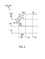
- FIG. 2 illustrates an exemplary negative pixel effect in a touch panel receiving a touch from a poorly grounded finger according to various embodiments.
- FIG. 3 illustrates an exemplary touch sensitive device according to various embodiments.
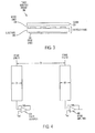
- FIG. 4 illustrates an exemplary sense line configuration in a touch panel according to various embodiments.
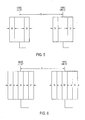
- FIG. 5 illustrates an exemplary split sense line configuration in a touch panel according to various embodiments.
- FIG. 6 illustrates another exemplary split sense line configuration in a touch panel according to various embodiments.
- FIG. 7 illustrates still another exemplary split sense line configuration in a touch panel according to various embodiments.
- FIG. 8 illustrates an exemplary method for negative pixel compensation using a split sense line configuration in a touch panel according to various embodiments.
- FIG. 9 illustrates an exemplary computing system that can include a touch panel with a split sense line configuration according to various embodiments.
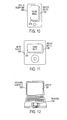
- FIG. 10 illustrates an exemplary mobile telephone that can include a touch panel with a split sense line configuration according to various embodiments.
- FIG. 11 illustrates an exemplary digital media player that can include a touch panel with a split sense line configuration according to various embodiments.
- FIG. 12 illustrates an exemplary portable computer that can include a touch panel with a split sense line configuration according to various embodiments.
- Negative pixel effect refers to a condition in which an undesirable capacitance can be introduced into the pancl to interfere with a touch or hover signal, causing the signal to be erroneous or otherwise distorted.
- the touch or hover signal can be generated as an indication of the proximity of the user or object to the panel at the same time that the poorly grounded user or object introduces the undesirable capacitance into the panel.
- the panel can be configured to include sense lines that are split lengthwise into multiple strips, thereby increasing touch signal capacitance in the sense lines in order to compensate for negative pixel capacitance introduced into the sense lines by the poorly grounded user or object.
- the multiple strips can be coupled together at a distal end to transmit a composite touch signal capacitance for processing. In some embodiments, the multiple strips can be separated at a distal end to transmit each strip's touch signal capacitance for processing.
- the ratio of the touch signal capacitance to the negative pixel capacitance can be maintained at a suitable level to compensate for the negative pixel effect.
- Negative pixel compensation in a touch panel can advantageously provide more accurate and faster touch or hover detection, as well as power savings, by not having to repeat measurements subject to poor grounding conditions. Additionally, the panel can more robustly adapt to various grounding conditions of a user or other object.
- ground can be used interchangeably to refer to good grounding conditions that can exist when an object is making a low impedance electrical coupling to the ground of the touch panel.
- FIG. 1 illustrates an exemplary schematic of a touch panel according to various embodiments.
- touch panel 100 can include an array of pixels 106 formed at the crossing points of drive lines 102 and sense lines 104. Each pixel 106 can have an associated mutual capacitance Csig 114 formed between the crossing drive lines 102 and sense lines 104.
- the drive lines 102 can be stimulated by stimulation signals 101 provided by drive circuitry (not shown) and the sense lines 104 can transmit sense signals 103, indicative of an object touching or hovering over the panel 100, to sense circuitry (not shown) that can include a sense amplifier for each sense line.
- the finger When a well grounded user's finger (or other object) touches or hovers over the panel 100, the finger can cause the capacitance Csig 114 to reduce by an amount ⁇ Csig at the touch or hover location.
- This capacitance change ⁇ Csig can be caused by the finger blocking electric fringe fields formed between the stimulated drive line 102 and crossing sense line 104, thereby shunting charge or current from the drive line through the finger to ground rather than being coupled to the sense line at the touch or hover location.
- the sense signals 103 representative of the capacitance change ⁇ Csig can be transmitted by the sense lines 104 to the sense circuitry for processing.
- the sense signals 103 can indicate the pixel where the touch or hover occurred and the "amount" of touch or hover that occurred at that pixel location.
- a finger capacitance Cfd to the stimulated drive line 102 can form a secondary capacitive path for coupling charge from the drive line to the sense line.
- Some of the charge generated by the stimulated drive line 102 and transmitted through the finger can be coupled via the secondary capacitive path back into the crossing sense line 104, rather than to ground.
- Csig may only be reduced by ( ⁇ Csig - Cneg), where Cneg can represent a so-called "negative capacitance” resulting from the charge coupled into the crossing sense line due to the finger's poor grounding.
- the sense signals 103 can still generally indicate the pixel where the touch or hover occurred but with an indication of a lesser amount of touch or hover than actually occurred. This is known as a negative pixel effect.
- FIG. 2 illustrates an exemplary negative pixel effect in a touch panel receiving a touch from a poorly grounded finger according to various embodiments.
- a poorly grounded finger (symbolically illustrated by a circle and identified as "finger") can touch at pixel 206a of touch panel 200.
- the capacitance along a first path between the drive line 202a and sense line 204a can be (Csig - ⁇ Csig).
- a second capacitive path can form between the drive line 202a and the sense line 204a, having capacitances Cfd (between the drive line 202a and the finger) and Cfs (between the sense line 204a and the finger).
- a capacitance Cgnd can also form between the finger and ground.
- the capacitances Cfd, Cfs, forming negative capacitance Cneg can be due to charge or current acquired by the finger from the stimulated drive line 202a being coupled back into the panel 200 at pixel 206a, rather than being shunted to ground.
- the outputted signal can be erroneous at a capacitance of (Csig - ⁇ Csig + Cneg) as a result of this negative pixel effect.
- the negative pixel effect can be further exacerbated by multiple poorly grounded user's fingers (or other objects) simultaneously touching or hovering over the panel 200 at different locations.
- Erroneous sense signals 103 like that described previously can be outputted at the touch or hover locations.
- phantom sense signals can be outputted at locations where there is no touch or hover (e.g., at sense lines 204b, 204c).
- the impact of the negative pixel effect can be a function of the proximity of the poorly grounded object to the touch panel. Because capacitance is inversely proportional to distance, the closer the poorly grounded object to the touch panel, the stronger the negative capacitance and, hence, the negative pixel effect. This can be a particular concern as touch sensitive devices become thinner, making the distance between the touching or hovering object and the touch panel closer.
- FIG. 3 illustrates an exemplary touch sensitive device according to various embodiments.
- touch sensitive device 300 can include thin cover 320 disposed over touch panel 310.
- the cover 320 can be made of glass, polymer, or some other suitable material.
- the panel 310 can include sense lines 304, drive lines 302, and substrate 335 to support the drive and sense lines.
- a user can touch or hover over a touchable surface of the cover 320 and the panel 310 can detect the touching or hovering user.
- the cover 320 can be quite thin, shortening the distance between the user and the panel 310. As a result, when the user is poorly grounded, the negative pixel effect can be more impactful on sense signals generated by the panel 310.
- compensating the sense signals for the negative pixel effect in a thinner touch sensitive device can improve touch or hover sensing of the device's touch panel in poor grounding conditions.
- the amount of the capacitance change ⁇ Csig can be likewise increased. That is, by increasing the amount of ⁇ Csig with the increased negative capacitances Cfd, Cfs, the ratio of ⁇ Csig to Cfd, Cfs can remain approximately the same as in normal operation (i.e., when the proximate object is well grounded), thereby attenuating the negative pixel effect of the increased Cfd, Cfs.
- the ratio is shown in the following Equation. ⁇ ⁇ Csig Cfd ⁇ Cfs Cfd + Cfs + Cgnd .
- the ratio can have a value in which the numerator of ⁇ Csig is considerably larger than the denominator of negative capacitances such that the sense signal, indicated by ⁇ Csig, is easily detected.
- the numerator can be at least 60% larger than the denominator.
- the touch panel can be configured to increase ⁇ Csig so as to maintain approximately the same ratio with the denominator.
- ⁇ Csig can be increased by increasing the number of sense lines in a touch panel, thereby providing more sense line edges around which to form more electric fringe fields.
- ⁇ Csig there are more fringe fields with which the touching or hovering object can interfere and/or block. The more fringe field interference or blocking by the object, the greater ⁇ Csig.
- both ⁇ Csig and the negative capacitance can dynamically increase because of the inverse relationship between capacitance and distance. That is, the closer the capacitive objects, the stronger the capacitance therebetween.
- the ratio between ⁇ Csig and the negative capacitance can be maintained (as illustrated in the previous Equation), such that ⁇ Csig is substantially larger than the negative capacitance.
- FIG. 4 illustrates an exemplary configuration of sense lines in a touch panel according to various embodiments.
- sense lines S1, S2 can form a typical configuration in which each sense line is a single line, rather than being split into multiple strips.
- Each sense line S1, S2 can have a width D2 and be connected to respective sense amplifiers 484, 485 for processing sense signals.
- the sense lines can be separated by distance D1.
- This typical configuration can be more susceptible to the negative pixel effect when placed in a thinner touch sensitive device. This is because the number of sense lines may be insufficient to produce a ⁇ Csig large enough to compensate for negative capacitance caused by a poorly grounded proximate object.
- FIG. 5 illustrates an exemplary configuration of sense lines that can compensate for the negative pixel effect that may be found in the typical configuration of FIG. 4 .
- sense line S1' can be split into multiple strips, thereby increasing the number of sense lines and the amount of ⁇ Csig so as to compensate for the negative pixel effect.
- the strips can have different widths, where the total width equals D2.
- the two strips can be coupled together at the distal ends and connected to sense amplifier 484 (not shown) for processing sense signals.
- Sense line S2' can be similarly divided into two strips coupled together at the distal ends and connected to sense amplifier 485 (not shown).
- the multiple strips in FIG. 5 can approximately double the electric fringe fields of the single sense lines in FIG. 4 , thereby effectively doubling ⁇ Csig to compensate for the negative pixel effect when a poorly grounded object touches or hovers over the panel.
- FIG. 6 illustrates another exemplary configuration of sense lines that can compensate for the negative pixel effect that may be found in the typical configuration of FIG. 4 .
- the three strips can be coupled together at the distal ends and connected at to sense amplifier 484 (not shown) for processing sense signals.
- Sense line S2" can be similarly configured.
- the multiple strips in FIG. 6 can approximately triple the electric fringe fields of the single sense lines in FIG. 4 , thereby effectively tripling ⁇ Csig to compensate for the negative pixel effect when a poorly grounded object touches or hovers over the panel.
- FIG. 7 illustrates another exemplary configuration of sense lines that can compensate for the negative pixel effect that may be found in the typical configuration of FIG. 4 .
- the example of FIG. 7 is similar to the example of FIG. 6 with the addition of multiplexer 738.
- sense line S1"' can have the three strips coupled together at the top distal end and separate at the bottom distal end, where each strip can input to the multiplexer 738.
- the multiplexer 738 can then select (using control signal SEL) one of the strips to transmit sense signals to sense amplifier 484 (not shown) for processing.
- FIGs. 5 through 7 show two or three strips, it is to be understood that a sense line can be split into any number of strips so as to compensate for negative pixel effect according to various embodiments.
- FIG. 8 illustrates an exemplary method to compensate for negative pixel effect in a touch panel according to various embodiments.
- a first capacitive path can form between a drive line and multiple sense line strips of a touch panel (810).
- the capacitive path can have touch capacitance (Csig - ⁇ Csig), when a well grounded object touches or hovers over the panel.
- the capacitive path can have touch capacitance (Csig - ⁇ Csig + Cneg), when a poorly grounded object touches or hovers over the panel.
- a second capacitive path can form between the drive line, the object, and the sense line strips (820).
- the capacitive path can have negative capacitance Cneg, which can include capacitance Cfd, formed between the drive line and the object, and capacitance Cfs, formed between the object and the sense line strips.
- Cneg negative capacitance
- the second capacitive path may be negligibly weak.
- ⁇ Csig increases in a configuration with multiple strips of sense lines, the ⁇ Csig increase can effectively counter the negative capacitance Cneg, thereby compensating for the negative pixel effect at the panel (830).
- FIG. 9 illustrates an exemplary computing system 900 that can have a touch panel configured to compensate for negative pixel effect according to various embodiments.
- computing system 900 can include touch controller 906.
- the touch controller 906 can be a single application specific integrated circuit (ASIC) that can include one or more processor subsystems 902, which can include one or more main processors, such as ARM968 processors or other processors with similar functionality and capabilities.
- main processors such as ARM968 processors or other processors with similar functionality and capabilities.
- the processor functionality can be implemented instead by dedicated logic, such as a state machine.
- the processor subsystems 902 can also include peripherals (not shown) such as random access memory (RAM) or other types of memory or storage, watchdog timers and the like.
- RAM random access memory
- the touch controller 906 can also include receive section 907 for receiving signals, such as touch signals 903 of one or more sense channels (not shown), other signals from other sensors such as sensor 911, etc.
- the touch controller 906 can also include demodulation section 909 such as a multistage vector demodulation engine, panel scan logic 910, and transmit section 914 for transmitting stimulation signals 916 to touch sensor panel 924 to drive the panel.
- the panel scan logic 910 can access RAM 912, autonomously read data from the sense channels, and provide control for the sense channels.
- the panel scan logic 910 can control the transmit section 914 to generate the stimulation signals 916 at various frequencies and phases that can be selectively applied to rows of the touch sensor panel 924.
- the touch controller 906 can also include charge pump 915, which can be used to generate the supply voltage for the transmit section 914.
- the stimulation signals 916 can have amplitudes higher than the maximum voltage by cascading two charge store devices, e.g., capacitors, together to form the charge pump 915. Therefore, the stimulus voltage can be higher (e.g., 6V) than the voltage level a single capacitor can handle (e.g., 3.6 V).
- FIG. 9 shows the charge pump 915 separate from the transmit section 914, the charge pump can be part of the transmit section.
- Touch sensor panel 924 can include a capacitive sensing medium having drive lines and multiple strips of sense lines according to various embodiments.
- the drive and sense line strips can be formed from a transparent conductive medium such as Indium Tin Oxide (ITO) or Antimony Tin Oxide (ATO), although other transparent and non-transparent materials such as copper can also be used.
- ITO Indium Tin Oxide
- ATO Antimony Tin Oxide
- the drive lines and sense line strips can be formed on a single side of a substantially transparent substrate separated by a substantially transparent dielectric material, on opposite sides of the substrate, on two separate substrates separated by the dielectric material, etc.
- Computing system 900 can also include host processor 928 for receiving outputs from the processor subsystems 902 and performing actions based on the outputs that can include, but are not limited to, moving an object such as a cursor or pointer, scrolling or panning, adjusting control settings, opening a file or document, viewing a menu, making a selection, executing instructions, operating a peripheral device coupled to the host device, answering a telephone call, placing a telephone call, terminating a telephone call, changing the volume or audio settings, storing information related to telephone communications such as addresses, frequently dialed numbers, received calls, missed calls, logging onto a computer or a computer network, permitting authorized individuals access to restricted areas of the computer or computer network, loading a user profile associated with a user's preferred arrangement of the computer desktop, permitting access to web content, launching a particular program, encrypting or decoding a message, and/or the like.
- host processor 928 for receiving outputs from the processor subsystems 902 and performing actions based on the outputs that can include, but
- the host processor 928 can also perform additional functions that may not be related to panel processing, and can be coupled to program storage 932 and display device 930 such as an LCD display for providing a UI to a user of the device.
- the host processor 928 can be a separate component from the touch controller 906, as shown.
- the host processor 928 can be included as part of the touch controller 906.
- the functions of the host processor 928 can be performed by the processor subsystem 902 and/or distributed among other components of the touch controller 906.
- the display device 930 together with the touch sensor panel 924, when located partially or entirely under the touch sensor panel or when integrated with the touch sensor panel, can form a touch sensitive device such as a touch screen.
- firmware stored in memory (e.g., one of the peripherals) and executed by the processor subsystem 902, or stored in the program storage 932 and executed by the host processor 928.
- the firmware can also be stored and/or transported within any non-transitory computer readable storage medium for use by or in connection with an instruction execution system, apparatus, or device, such as a computer-based system, processor-containing system, or other system that can fetch the instructions from the instruction execution system, apparatus, or device and execute the instructions.
- a "non-transitory computer readable storage medium" can be any non-transitory medium that can contain or store the program for use by or in connection with the instruction execution system, apparatus, or device.
- the non-transitory computer readable storage medium can include, but is not limited to, an electronic, magnetic, optical, electromagnetic, infrared, or semiconductor system, apparatus or device, a portable computer diskette (magnetic), a random access memory (RAM) (magnetic), a read-only memory (ROM) (magnetic), an erasable programmable read-only memory (EPROM) (magnetic), a portable optical disc such a CD, CD-R, CD-RW, DVD, DVD-R, or DVD-RW, or flash memory such as compact flash cards, secured digital cards, USB memory devices, memory sticks, and the like.
- the firmware can also be propagated within any transport medium for use by or in connection with an instruction execution system, apparatus, or device, such as a computer-based system, processor-containing system, or other system that can fetch the instructions from the instruction execution system, apparatus, or device and execute the instructions.
- a "transport medium" can be any non-transitory medium that can communicate, propagate or transport the program for use by or in connection with the instruction execution system, apparatus, or device.
- the transport medium can include, but is not limited to, an electronic, magnetic, optical, electromagnetic or infrared wired or wireless propagation medium.
- the touch panel is not limited to touch, as described in FIG. 9 , but can be a proximity panel or any other panel according to various embodiments.
- the touch sensor panel described herein can be either a single-touch or a multi-touch sensor panel.
- the computing system is not limited to the components and configuration of FIG. 9 , but can include other and/or additional components in various configurations capable of compensating for a negative pixel effect according to various embodiments.
- FIG. 10 illustrates an exemplary mobile telephone 1000 that can include touch sensor panel 1024, display 1036, and other computing system blocks, where the panel can be configured with multiple sense line strips to compensate for negative pixel effect according to various embodiments.
- FIG. 11 illustrate an exemplary digital media player 1100 that can include touch sensor panel 1124, display 1136, and other computing system blocks, where the panel can be configured with multiple sense line strips to compensate for negative pixel effect according to various embodiments.
- FIG. 12 illustrates an exemplary personal computer 1200 that can include touch sensor panel (trackpad) 1224, display 1236, and other computing system blocks, where the panel can be configured with multiple sense line strips to compensate for negative pixel effect according to various embodiments.
- touch sensor panel trackpad
- display 1236 display 1236
- other computing system blocks where the panel can be configured with multiple sense line strips to compensate for negative pixel effect according to various embodiments.
- the mobile telephone, media player, and personal computer of FIGs. 10 through 12 can realize power savings, improved accuracy, faster speed, and more robustness by compensating for a negative pixel effect according to various embodiments.
- some examples of the disclosure are directed to a touch panel comprising: a sense line split into multiple strips, the strips configured to form a first capacitance indicative of a proximity of an object to the panel and a second capacitance indicative of a grounding condition of the object, the first capacitance being substantially larger than the second capacitance so as to compensate for negative pixel effect at the panel.
- the sense line is split lengthwise into the strips.
- the strips of the sense line are coupled together at distal ends.
- the number of strips is at least two.
- the strips have substantially the same width. Additionally or alternatively to one or more of the examples disclosed above, in some examples the strips of the sense line are coupled at one distal end and separate at the other distal end, the panel comprising a multiplexor coupled to the strips at the other distal end and configured to select between the strips to output a signal therefrom. Additionally or alternatively to one or more of the examples disclosed above, in some examples the strips are configured to form the first capacitance with a drive line for driving the panel and the strips are configured to form the second capacitance with the drive line and the object.
- the multiplicity of the strips causes the first capacitance to have an increased value so as to compensate for the negative pixel effect.
- the panel can be incorporated into at least one of a mobile telephone, a digital media player, or a portable computer.
- Some examples of the disclosure are directed to a touch panel comprising: a drive line configured to drive the device to sense a proximate object; and a sense line divided lengthwise into multiple strips coupled at a distal end, the multiple strips configured to sense the proximate object, wherein the drive line and the strips form a capacitance for compensating for negative pixel effect at the panel.
- the drive line and the strips form electric fringe fields, the number of fields related to the number of strips.
- the fringe fields are configured to be interfered with by the proximate object, the amount of interference corresponding to the capacitance.
- a second capacitance forms between the drive line, the strips, and the proximate object to create the negative pixel effect.
- Some examples of the disclosure are directed to a touch sensitive device comprising: a cover having a touchable surface; and a touch panel proximate to a surface of the cover opposite the touchable surface, the touch panel including multiple drive lines configured to drive the panel to detect an object proximate to the touchable surface, and multiple sense lines configured to sense the proximate object, each sense line divided into multiple strips to form multiple capacitances for compensating for negative pixel effect at the panel. Additionally or alternatively to one or more of the examples disclosed above, in some examples the multiple capacitances are mutual capacitances.
- the multiple capacitances form between the drive lines and the strips, indicative of a proximity of the object, wherein second capacitances form between the drive lines, the strips, and the proximate object, indicative of the negative pixel effect, and wherein the multiple capacitances are substantially larger than the second capacitances so as to compensate for the negative pixel effect at the panel.
- the strength of the negative pixel effect is a function of thinness of the cover.
- Some examples of the disclosure are directed to a method to reduce negative pixel effect in a touch panel, comprising: forming a first capacitive path between a drive line of the panel and a sense line of the panel, the sense line split into multiple strips; forming a second capacitive path between the drive line, the strips of the sense line, and the proximate object; and providing a first capacitance, indicative of a proximity of the object, along the first capacitive path and a second capacitance, indicative of a grounding condition of the object, along the second capacitive path, wherein the first capacitance is substantially larger than the second capacitance so as to compensate for negative pixel effect at the panel caused by the grounding condition.
- forming the first capacitive path comprises capacitively coupling the drive line and the sense line together to create the first capacitance.
- forming the second capacitive path comprises: forming a third capacitive path capacitively coupling the drive line and the proximate object; forming a fourth capacitive path capacitively coupling the strips and the proximate object; and coupling the third and fourth capacitive paths together to form the second capacitive path for the second capacitance.
- the method further comprises maintaining a ratio between the first and second capacitances in which the first capacitance is substantially larger than the second capacitance, regardless of a proximity of the object to the panel. Additionally or alternatively to one or more of the examples disclosed above, in some examples maintaining the ratio comprises dynamically increasing the first capacitance in conjunction with the second capacitance as the proximate object approaches the panel so as to maintain the ratio at a predetermined level to compensate for the negative pixel effect.
- the negative pixel effect is a function of the grounding condition indicated by the second capacitance and wherein the negative pixel effect is compensated for by reducing the effect of the second capacitance at the panel.
Landscapes
- Engineering & Computer Science (AREA)
- General Engineering & Computer Science (AREA)
- Theoretical Computer Science (AREA)
- Human Computer Interaction (AREA)
- Physics & Mathematics (AREA)
- General Physics & Mathematics (AREA)
- Quality & Reliability (AREA)
- Position Input By Displaying (AREA)
Applications Claiming Priority (1)
| Application Number | Priority Date | Filing Date | Title |
|---|---|---|---|
| US13/406,338 US9081442B2 (en) | 2012-02-27 | 2012-02-27 | Split sense lines for negative pixel compensation |
Publications (2)
| Publication Number | Publication Date |
|---|---|
| EP2631750A2 true EP2631750A2 (de) | 2013-08-28 |
| EP2631750A3 EP2631750A3 (de) | 2014-06-25 |
Family
ID=47790717
Family Applications (1)
| Application Number | Title | Priority Date | Filing Date |
|---|---|---|---|
| EP13156753.9A Ceased EP2631750A3 (de) | 2012-02-27 | 2013-02-26 | Geteilte Abfrageleitungen für negativen Pixelausgleich |
Country Status (6)
| Country | Link |
|---|---|
| US (2) | US9081442B2 (de) |
| EP (1) | EP2631750A3 (de) |
| KR (1) | KR101525659B1 (de) |
| CN (3) | CN203250300U (de) |
| AU (2) | AU2013100141B4 (de) |
| TW (1) | TWI536232B (de) |
Families Citing this family (9)
| Publication number | Priority date | Publication date | Assignee | Title |
|---|---|---|---|---|
| US8692777B2 (en) * | 2008-02-08 | 2014-04-08 | Apple Inc. | Method for rapidly testing capacitance sensing array fault conditions using a floating conductor |
| US20130207913A1 (en) * | 2012-02-09 | 2013-08-15 | Sony Mobile Communications Inc. | Touch panel device, portable terminal, position detecting method, and recording medium |
| US9081442B2 (en) * | 2012-02-27 | 2015-07-14 | Apple Inc. | Split sense lines for negative pixel compensation |
| KR20170118601A (ko) * | 2016-04-15 | 2017-10-25 | 가부시키가이샤 한도오따이 에네루기 켄큐쇼 | 표시 장치, 입출력 장치, 정보 처리 장치 |
| JP2018004927A (ja) * | 2016-07-01 | 2018-01-11 | 株式会社半導体エネルギー研究所 | 表示装置、入出力装置、情報処理装置、表示方法 |
| CN108196739A (zh) * | 2018-01-24 | 2018-06-22 | 北京硬壳科技有限公司 | 一种触控板 |
| US10845930B2 (en) | 2018-09-28 | 2020-11-24 | Apple Inc. | Common mode noise mitigation for integrated touch screens |
| KR102350234B1 (ko) * | 2021-02-13 | 2022-01-12 | 이성호 | 정전용량 검출장치 |
| US20240219209A1 (en) * | 2022-12-30 | 2024-07-04 | Ohio State Innovation Foundation | Embedded sensors |
Family Cites Families (52)
| Publication number | Priority date | Publication date | Assignee | Title |
|---|---|---|---|---|
| GB1442841A (en) * | 1973-11-13 | 1976-07-14 | Secr Defence | Charge coupled devices |
| US4543500A (en) * | 1978-09-22 | 1985-09-24 | Texas Instruments Incorporated | High performance dynamic sense amplifier voltage boost for row address lines |
| US5483261A (en) | 1992-02-14 | 1996-01-09 | Itu Research, Inc. | Graphical input controller and method with rear screen image detection |
| US5880411A (en) | 1992-06-08 | 1999-03-09 | Synaptics, Incorporated | Object position detector with edge motion feature and gesture recognition |
| US5488204A (en) | 1992-06-08 | 1996-01-30 | Synaptics, Incorporated | Paintbrush stylus for capacitive touch sensor pad |
| JPH07129304A (ja) | 1993-11-05 | 1995-05-19 | Seiko Instr Inc | 座標入力装置 |
| US5825352A (en) | 1996-01-04 | 1998-10-20 | Logitech, Inc. | Multiple fingers contact sensing method for emulating mouse buttons and mouse operations on a touch sensor pad |
| US5835079A (en) | 1996-06-13 | 1998-11-10 | International Business Machines Corporation | Virtual pointing device for touchscreens |
| US6310610B1 (en) | 1997-12-04 | 2001-10-30 | Nortel Networks Limited | Intelligent touch display |
| US7663607B2 (en) | 2004-05-06 | 2010-02-16 | Apple Inc. | Multipoint touchscreen |
| US8479122B2 (en) | 2004-07-30 | 2013-07-02 | Apple Inc. | Gestures for touch sensitive input devices |
| KR100595926B1 (ko) | 1998-01-26 | 2006-07-05 | 웨인 웨스터만 | 수동 입력 통합 방법 및 장치 |
| US6188391B1 (en) | 1998-07-09 | 2001-02-13 | Synaptics, Inc. | Two-layer capacitive touchpad and method of making same |
| JP4542637B2 (ja) | 1998-11-25 | 2010-09-15 | セイコーエプソン株式会社 | 携帯情報機器及び情報記憶媒体 |
| US6700392B2 (en) * | 2001-02-02 | 2004-03-02 | Wayne C. Haase | Digital measurement circuit and system using a grounded capacitive sensor |
| JP3800984B2 (ja) | 2001-05-21 | 2006-07-26 | ソニー株式会社 | ユーザ入力装置 |
| JP2003173237A (ja) | 2001-09-28 | 2003-06-20 | Ricoh Co Ltd | 情報入出力システム、プログラム及び記憶媒体 |
| US6690387B2 (en) | 2001-12-28 | 2004-02-10 | Koninklijke Philips Electronics N.V. | Touch-screen image scrolling system and method |
| US11275405B2 (en) | 2005-03-04 | 2022-03-15 | Apple Inc. | Multi-functional hand-held device |
| KR100481856B1 (ko) * | 2002-08-14 | 2005-04-11 | 삼성전자주식회사 | 이이피롬 및 마스크롬을 구비하는 반도체 장치 및 그 제조방법 |
| JP3701661B2 (ja) * | 2003-12-05 | 2005-10-05 | シャープ株式会社 | 表示パネルおよび表示装置 |
| US20050122119A1 (en) | 2003-12-05 | 2005-06-09 | Touchram Llc | Low noise proximity sensing system |
| US20070291016A1 (en) * | 2006-06-20 | 2007-12-20 | Harald Philipp | Capacitive Position Sensor |
| US7855718B2 (en) * | 2007-01-03 | 2010-12-21 | Apple Inc. | Multi-touch input discrimination |
| CN101681223A (zh) * | 2007-05-07 | 2010-03-24 | 爱特梅尔公司 | 二维位置传感器 |
| US8358276B2 (en) * | 2007-12-21 | 2013-01-22 | Apple Inc. | Touch pad electrode design |
| EP2113827B8 (de) | 2008-04-30 | 2018-09-19 | InnoLux Corporation | Berührungseingabevorrichtung |
| US8726497B2 (en) | 2008-08-01 | 2014-05-20 | 3M Innovative Properties Company | Methods of making composite electrodes |
| US8810542B2 (en) * | 2008-09-10 | 2014-08-19 | Apple Inc. | Correction of parasitic capacitance effect in touch sensor panels |
| US8692776B2 (en) * | 2008-09-19 | 2014-04-08 | Apple Inc. | Correction of parasitic capacitance effect in touch sensor panels |
| US20100110040A1 (en) * | 2008-10-30 | 2010-05-06 | Samsung Electronics Co., Ltd. | Touch controller having increased sensing sensitivity, and display driving circuit and display device and system having the touch controller |
| US8654092B2 (en) | 2009-01-26 | 2014-02-18 | Sharp Kabushiki Kaisha | Touch panel incorporating display device |
| JP2010282539A (ja) * | 2009-06-08 | 2010-12-16 | Sanyo Electric Co Ltd | 静電容量型タッチセンサ用の信号処理回路 |
| JP5486854B2 (ja) * | 2009-06-29 | 2014-05-07 | 株式会社ジャパンディスプレイ | 情報入力装置、表示装置 |
| JP4756403B2 (ja) * | 2009-06-30 | 2011-08-24 | カシオ計算機株式会社 | 光源装置及びプロジェクタ |
| US8482544B2 (en) | 2009-07-10 | 2013-07-09 | Apple Inc. | Negative pixel compensation |
| US9632622B2 (en) * | 2009-07-16 | 2017-04-25 | Apple Inc. | Ground detection for touch sensitive device |
| TWI395006B (zh) * | 2009-09-09 | 2013-05-01 | Au Optronics Corp | 觸控顯示面板 |
| US8749512B2 (en) * | 2009-09-30 | 2014-06-10 | Apple Inc. | Negative pixel compensation |
| US20110102331A1 (en) | 2009-10-29 | 2011-05-05 | Qrg Limited | Redundant touchscreen electrodes |
| US20110100727A1 (en) | 2009-10-30 | 2011-05-05 | Shin John Choi | Touch Sensitive Device with Dielectric Layer |
| US8194047B2 (en) | 2009-11-16 | 2012-06-05 | Au Optronics Corporation | Multi-channel touch panel |
| KR101085776B1 (ko) * | 2010-01-15 | 2011-11-21 | 삼성전자주식회사 | 터치 패널 및 그 터치 패널을 이용한 입력 인식 장치 |
| CN102135827B (zh) * | 2010-01-21 | 2015-01-07 | 苹果公司 | 补偿负像素效应的方法和设备、触摸敏感设备及终端设备 |
| US8581879B2 (en) | 2010-01-21 | 2013-11-12 | Apple Inc. | Negative pixel compensation |
| KR101109382B1 (ko) | 2010-04-12 | 2012-01-30 | 삼성전기주식회사 | 터치패널 |
| CN101840286B (zh) * | 2010-04-30 | 2013-04-17 | 友达光电股份有限公司 | 触控面板 |
| US8482546B2 (en) | 2010-06-30 | 2013-07-09 | Cypress Semiconductor Corporation | Self shielding capacitance sensing panel |
| US8723834B2 (en) * | 2010-07-28 | 2014-05-13 | Atmel Corporation | Touch sensitive screen configurations |
| TWI471796B (zh) * | 2011-02-11 | 2015-02-01 | Wintek Corp | 觸控顯示裝置 |
| US20130057229A1 (en) * | 2011-09-02 | 2013-03-07 | Intersil Americas Inc. | Power factor correction apparatus and method |
| US9081442B2 (en) * | 2012-02-27 | 2015-07-14 | Apple Inc. | Split sense lines for negative pixel compensation |
-
2012
- 2012-02-27 US US13/406,338 patent/US9081442B2/en active Active
-
2013
- 2013-02-11 AU AU2013100141A patent/AU2013100141B4/en not_active Expired
- 2013-02-11 AU AU2013200693A patent/AU2013200693B2/en not_active Ceased
- 2013-02-25 CN CN2013201884532U patent/CN203250300U/zh not_active Expired - Fee Related
- 2013-02-25 CN CN201710139451.7A patent/CN106919288B/zh not_active Expired - Fee Related
- 2013-02-25 CN CN201310128172.2A patent/CN103294261B/zh not_active Expired - Fee Related
- 2013-02-26 KR KR1020130020718A patent/KR101525659B1/ko not_active Expired - Fee Related
- 2013-02-26 EP EP13156753.9A patent/EP2631750A3/de not_active Ceased
- 2013-02-27 TW TW102107076A patent/TWI536232B/zh not_active IP Right Cessation
-
2015
- 2015-06-11 US US14/737,424 patent/US11163399B2/en not_active Expired - Fee Related
Non-Patent Citations (1)
| Title |
|---|
| None |
Also Published As
| Publication number | Publication date |
|---|---|
| US20150277664A1 (en) | 2015-10-01 |
| AU2013100141B4 (en) | 2013-03-28 |
| TWI536232B (zh) | 2016-06-01 |
| CN103294261B (zh) | 2017-03-01 |
| KR101525659B1 (ko) | 2015-06-03 |
| AU2013200693A1 (en) | 2013-09-12 |
| AU2013100141A4 (en) | 2013-03-07 |
| TW201342180A (zh) | 2013-10-16 |
| EP2631750A3 (de) | 2014-06-25 |
| KR20130098222A (ko) | 2013-09-04 |
| US20130222324A1 (en) | 2013-08-29 |
| US11163399B2 (en) | 2021-11-02 |
| US9081442B2 (en) | 2015-07-14 |
| CN106919288B (zh) | 2022-02-11 |
| CN103294261A (zh) | 2013-09-11 |
| AU2013200693B2 (en) | 2015-01-22 |
| CN106919288A (zh) | 2017-07-04 |
| CN203250300U (zh) | 2013-10-23 |
Similar Documents
| Publication | Publication Date | Title |
|---|---|---|
| AU2013100141B4 (en) | Split sense lines for negative pixel compensation | |
| US8482544B2 (en) | Negative pixel compensation | |
| US10282026B2 (en) | Measuring body capacitance effect in touch sensitive device | |
| US9013437B2 (en) | Negative pixel compensation | |
| EP2413224B1 (de) | Kapazitätsänderungsausgleich in berührungsempfindlichen Vorrichtungen | |
| US8810542B2 (en) | Correction of parasitic capacitance effect in touch sensor panels | |
| US20110100727A1 (en) | Touch Sensitive Device with Dielectric Layer | |
| AU2015202077B2 (en) | Split sense lines for negative pixel compensation | |
| AU2012227270B2 (en) | Negative pixel compensation | |
| HK1153557A (en) | Negative pixel compensation |
Legal Events
| Date | Code | Title | Description |
|---|---|---|---|
| PUAI | Public reference made under article 153(3) epc to a published international application that has entered the european phase |
Free format text: ORIGINAL CODE: 0009012 |
|
| 17P | Request for examination filed |
Effective date: 20130226 |
|
| AK | Designated contracting states |
Kind code of ref document: A2 Designated state(s): AL AT BE BG CH CY CZ DE DK EE ES FI FR GB GR HR HU IE IS IT LI LT LU LV MC MK MT NL NO PL PT RO RS SE SI SK SM TR |
|
| AX | Request for extension of the european patent |
Extension state: BA ME |
|
| PUAL | Search report despatched |
Free format text: ORIGINAL CODE: 0009013 |
|
| AK | Designated contracting states |
Kind code of ref document: A3 Designated state(s): AL AT BE BG CH CY CZ DE DK EE ES FI FR GB GR HR HU IE IS IT LI LT LU LV MC MK MT NL NO PL PT RO RS SE SI SK SM TR |
|
| AX | Request for extension of the european patent |
Extension state: BA ME |
|
| RIC1 | Information provided on ipc code assigned before grant |
Ipc: G06F 3/041 20060101AFI20140522BHEP Ipc: G06F 3/044 20060101ALI20140522BHEP |
|
| 17Q | First examination report despatched |
Effective date: 20140610 |
|
| STAA | Information on the status of an ep patent application or granted ep patent |
Free format text: STATUS: THE APPLICATION HAS BEEN REFUSED |
|
| 18R | Application refused |
Effective date: 20170119 |