EP2624020A1 - Optical substrate - Google Patents
Optical substrate Download PDFInfo
- Publication number
- EP2624020A1 EP2624020A1 EP12188115.5A EP12188115A EP2624020A1 EP 2624020 A1 EP2624020 A1 EP 2624020A1 EP 12188115 A EP12188115 A EP 12188115A EP 2624020 A1 EP2624020 A1 EP 2624020A1
- Authority
- EP
- European Patent Office
- Prior art keywords
- layer
- antireflection film
- optical substrate
- film
- substrate according
- Prior art date
- Legal status (The legal status is an assumption and is not a legal conclusion. Google has not performed a legal analysis and makes no representation as to the accuracy of the status listed.)
- Withdrawn
Links
- 239000000758 substrate Substances 0.000 title claims abstract description 51
- 230000003287 optical effect Effects 0.000 title claims abstract description 28
- 230000002787 reinforcement Effects 0.000 claims abstract description 21
- 230000003373 anti-fouling effect Effects 0.000 claims abstract description 17
- 238000005336 cracking Methods 0.000 claims abstract description 8
- 239000010408 film Substances 0.000 claims description 95
- VYPSYNLAJGMNEJ-UHFFFAOYSA-N Silicium dioxide Chemical compound O=[Si]=O VYPSYNLAJGMNEJ-UHFFFAOYSA-N 0.000 claims description 54
- ZKATWMILCYLAPD-UHFFFAOYSA-N niobium pentoxide Chemical compound O=[Nb](=O)O[Nb](=O)=O ZKATWMILCYLAPD-UHFFFAOYSA-N 0.000 claims description 36
- 239000000463 material Substances 0.000 claims description 35
- 239000000377 silicon dioxide Substances 0.000 claims description 22
- 229910052681 coesite Inorganic materials 0.000 claims description 21
- 229910052906 cristobalite Inorganic materials 0.000 claims description 21
- 229910052682 stishovite Inorganic materials 0.000 claims description 21
- 229910052905 tridymite Inorganic materials 0.000 claims description 21
- 239000012788 optical film Substances 0.000 claims description 17
- 229910001635 magnesium fluoride Inorganic materials 0.000 claims description 15
- MCMNRKCIXSYSNV-UHFFFAOYSA-N Zirconium dioxide Chemical compound O=[Zr]=O MCMNRKCIXSYSNV-UHFFFAOYSA-N 0.000 claims description 14
- 230000003595 spectral effect Effects 0.000 claims description 12
- 229910052814 silicon oxide Inorganic materials 0.000 claims description 10
- GWEVSGVZZGPLCZ-UHFFFAOYSA-N Titan oxide Chemical compound O=[Ti]=O GWEVSGVZZGPLCZ-UHFFFAOYSA-N 0.000 claims description 8
- ORUIBWPALBXDOA-UHFFFAOYSA-L magnesium fluoride Chemical compound [F-].[F-].[Mg+2] ORUIBWPALBXDOA-UHFFFAOYSA-L 0.000 claims description 7
- 239000005871 repellent Substances 0.000 claims description 4
- 239000000203 mixture Substances 0.000 claims description 3
- PBCFLUZVCVVTBY-UHFFFAOYSA-N tantalum pentoxide Inorganic materials O=[Ta](=O)O[Ta](=O)=O PBCFLUZVCVVTBY-UHFFFAOYSA-N 0.000 claims description 2
- 230000001419 dependent effect Effects 0.000 abstract description 14
- 239000006059 cover glass Substances 0.000 abstract description 8
- 230000000694 effects Effects 0.000 abstract description 3
- 239000011521 glass Substances 0.000 description 18
- 238000000034 method Methods 0.000 description 14
- 238000010586 diagram Methods 0.000 description 11
- 150000002500 ions Chemical class 0.000 description 10
- 230000003666 anti-fingerprint Effects 0.000 description 6
- 239000000126 substance Substances 0.000 description 6
- 238000001771 vacuum deposition Methods 0.000 description 6
- PNEYBMLMFCGWSK-UHFFFAOYSA-N aluminium oxide Inorganic materials [O-2].[O-2].[O-2].[Al+3].[Al+3] PNEYBMLMFCGWSK-UHFFFAOYSA-N 0.000 description 4
- 230000000052 comparative effect Effects 0.000 description 4
- 229910052593 corundum Inorganic materials 0.000 description 4
- 230000001747 exhibiting effect Effects 0.000 description 4
- 229910001845 yogo sapphire Inorganic materials 0.000 description 4
- 238000005299 abrasion Methods 0.000 description 3
- 230000015572 biosynthetic process Effects 0.000 description 3
- 229910000484 niobium oxide Inorganic materials 0.000 description 3
- URLJKFSTXLNXLG-UHFFFAOYSA-N niobium(5+);oxygen(2-) Chemical compound [O-2].[O-2].[O-2].[O-2].[O-2].[Nb+5].[Nb+5] URLJKFSTXLNXLG-UHFFFAOYSA-N 0.000 description 3
- 230000001413 cellular effect Effects 0.000 description 2
- 239000011248 coating agent Substances 0.000 description 2
- 238000000576 coating method Methods 0.000 description 2
- 239000002184 metal Substances 0.000 description 2
- 229910052751 metal Inorganic materials 0.000 description 2
- 239000011347 resin Substances 0.000 description 2
- 229920005989 resin Polymers 0.000 description 2
- 238000004088 simulation Methods 0.000 description 2
- 238000002834 transmittance Methods 0.000 description 2
- PXGOKWXKJXAPGV-UHFFFAOYSA-N Fluorine Chemical compound FF PXGOKWXKJXAPGV-UHFFFAOYSA-N 0.000 description 1
- ATJFFYVFTNAWJD-UHFFFAOYSA-N Tin Chemical compound [Sn] ATJFFYVFTNAWJD-UHFFFAOYSA-N 0.000 description 1
- 230000002745 absorbent Effects 0.000 description 1
- 239000002250 absorbent Substances 0.000 description 1
- 239000003522 acrylic cement Substances 0.000 description 1
- 230000004913 activation Effects 0.000 description 1
- 239000000853 adhesive Substances 0.000 description 1
- 230000001070 adhesive effect Effects 0.000 description 1
- 125000000217 alkyl group Chemical group 0.000 description 1
- 150000001343 alkyl silanes Chemical class 0.000 description 1
- 238000006243 chemical reaction Methods 0.000 description 1
- 238000004140 cleaning Methods 0.000 description 1
- 238000000151 deposition Methods 0.000 description 1
- 230000008021 deposition Effects 0.000 description 1
- 238000003618 dip coating Methods 0.000 description 1
- 239000000428 dust Substances 0.000 description 1
- 239000012530 fluid Substances 0.000 description 1
- 229910052731 fluorine Inorganic materials 0.000 description 1
- 239000011737 fluorine Substances 0.000 description 1
- 125000001153 fluoro group Chemical group F* 0.000 description 1
- 230000007062 hydrolysis Effects 0.000 description 1
- 238000006460 hydrolysis reaction Methods 0.000 description 1
- 238000007733 ion plating Methods 0.000 description 1
- 239000003921 oil Substances 0.000 description 1
- 239000000049 pigment Substances 0.000 description 1
- 229920006254 polymer film Polymers 0.000 description 1
- 235000012239 silicon dioxide Nutrition 0.000 description 1
- 238000006884 silylation reaction Methods 0.000 description 1
- 238000004544 sputter deposition Methods 0.000 description 1
Images




Classifications
-
- G—PHYSICS
- G02—OPTICS
- G02B—OPTICAL ELEMENTS, SYSTEMS OR APPARATUS
- G02B1/00—Optical elements characterised by the material of which they are made; Optical coatings for optical elements
- G02B1/10—Optical coatings produced by application to, or surface treatment of, optical elements
- G02B1/11—Anti-reflection coatings
-
- G—PHYSICS
- G02—OPTICS
- G02B—OPTICAL ELEMENTS, SYSTEMS OR APPARATUS
- G02B1/00—Optical elements characterised by the material of which they are made; Optical coatings for optical elements
- G02B1/10—Optical coatings produced by application to, or surface treatment of, optical elements
- G02B1/11—Anti-reflection coatings
- G02B1/113—Anti-reflection coatings using inorganic layer materials only
- G02B1/115—Multilayers
-
- C—CHEMISTRY; METALLURGY
- C03—GLASS; MINERAL OR SLAG WOOL
- C03C—CHEMICAL COMPOSITION OF GLASSES, GLAZES OR VITREOUS ENAMELS; SURFACE TREATMENT OF GLASS; SURFACE TREATMENT OF FIBRES OR FILAMENTS MADE FROM GLASS, MINERALS OR SLAGS; JOINING GLASS TO GLASS OR OTHER MATERIALS
- C03C17/00—Surface treatment of glass, not in the form of fibres or filaments, by coating
- C03C17/34—Surface treatment of glass, not in the form of fibres or filaments, by coating with at least two coatings having different compositions
-
- C—CHEMISTRY; METALLURGY
- C03—GLASS; MINERAL OR SLAG WOOL
- C03C—CHEMICAL COMPOSITION OF GLASSES, GLAZES OR VITREOUS ENAMELS; SURFACE TREATMENT OF GLASS; SURFACE TREATMENT OF FIBRES OR FILAMENTS MADE FROM GLASS, MINERALS OR SLAGS; JOINING GLASS TO GLASS OR OTHER MATERIALS
- C03C17/00—Surface treatment of glass, not in the form of fibres or filaments, by coating
- C03C17/34—Surface treatment of glass, not in the form of fibres or filaments, by coating with at least two coatings having different compositions
- C03C17/3411—Surface treatment of glass, not in the form of fibres or filaments, by coating with at least two coatings having different compositions with at least two coatings of inorganic materials
- C03C17/3429—Surface treatment of glass, not in the form of fibres or filaments, by coating with at least two coatings having different compositions with at least two coatings of inorganic materials at least one of the coatings being a non-oxide coating
- C03C17/3447—Surface treatment of glass, not in the form of fibres or filaments, by coating with at least two coatings having different compositions with at least two coatings of inorganic materials at least one of the coatings being a non-oxide coating comprising a halide
- C03C17/3452—Surface treatment of glass, not in the form of fibres or filaments, by coating with at least two coatings having different compositions with at least two coatings of inorganic materials at least one of the coatings being a non-oxide coating comprising a halide comprising a fluoride
-
- G—PHYSICS
- G02—OPTICS
- G02B—OPTICAL ELEMENTS, SYSTEMS OR APPARATUS
- G02B1/00—Optical elements characterised by the material of which they are made; Optical coatings for optical elements
- G02B1/10—Optical coatings produced by application to, or surface treatment of, optical elements
- G02B1/11—Anti-reflection coatings
- G02B1/113—Anti-reflection coatings using inorganic layer materials only
-
- G—PHYSICS
- G02—OPTICS
- G02B—OPTICAL ELEMENTS, SYSTEMS OR APPARATUS
- G02B1/00—Optical elements characterised by the material of which they are made; Optical coatings for optical elements
- G02B1/10—Optical coatings produced by application to, or surface treatment of, optical elements
- G02B1/14—Protective coatings, e.g. hard coatings
-
- G—PHYSICS
- G02—OPTICS
- G02B—OPTICAL ELEMENTS, SYSTEMS OR APPARATUS
- G02B1/00—Optical elements characterised by the material of which they are made; Optical coatings for optical elements
- G02B1/10—Optical coatings produced by application to, or surface treatment of, optical elements
- G02B1/18—Coatings for keeping optical surfaces clean, e.g. hydrophobic or photo-catalytic films
-
- G—PHYSICS
- G02—OPTICS
- G02B—OPTICAL ELEMENTS, SYSTEMS OR APPARATUS
- G02B27/00—Optical systems or apparatus not provided for by any of the groups G02B1/00 - G02B26/00, G02B30/00
- G02B27/0006—Optical systems or apparatus not provided for by any of the groups G02B1/00 - G02B26/00, G02B30/00 with means to keep optical surfaces clean, e.g. by preventing or removing dirt, stains, contamination, condensation
-
- G—PHYSICS
- G02—OPTICS
- G02B—OPTICAL ELEMENTS, SYSTEMS OR APPARATUS
- G02B5/00—Optical elements other than lenses
- G02B5/20—Filters
- G02B5/28—Interference filters
- G02B5/285—Interference filters comprising deposited thin solid films
-
- C—CHEMISTRY; METALLURGY
- C03—GLASS; MINERAL OR SLAG WOOL
- C03C—CHEMICAL COMPOSITION OF GLASSES, GLAZES OR VITREOUS ENAMELS; SURFACE TREATMENT OF GLASS; SURFACE TREATMENT OF FIBRES OR FILAMENTS MADE FROM GLASS, MINERALS OR SLAGS; JOINING GLASS TO GLASS OR OTHER MATERIALS
- C03C2217/00—Coatings on glass
- C03C2217/70—Properties of coatings
- C03C2217/73—Anti-reflective coatings with specific characteristics
- C03C2217/734—Anti-reflective coatings with specific characteristics comprising an alternation of high and low refractive indexes
Definitions
- the invention relates to an optical substrate comprising a tone-adjustment antireflection film such as a cover glass for displays which is used for a touch panel. More particularly, the invention is concerned with an optical substrate that has, for example, a reinforcement layer, which is intended to prevent cracking, formed on a glass substrate, has an antiglare layer such as a microstructure formed on the reinforcement layer, and has the tone-adjustment antireflection film formed on the antiglare layer.
- a filter with an antireflection feature for display devices which has a reinforcement layer formed by performing reinforcement treatment on a glass substrate, and has a tone-adjustment antireflection film formed on the reinforcement layer has been known.
- an oxynitride tin film of 107 nm thick is formed as a first layer directly on a glass substrate, and a silicon dioxide film of 72 nm thick is further formed as a second layer in order to thus perform reinforcement treatment on the glass.
- a PET-coated reflective film that has undergone tone correction is bonded to the conductive film with an acrylic adhesive between them, whereby an antireflection filter is fabricated.
- a functional film (C) 40 is formed on a conductive mesh layer (B) 10 with a pigment-containing translucent adhesive (D) 30 between them.
- the functional film (C) 40 has a near-infrared absorbent containing layer 41, a polymer film 43, and an antireflection layer 42, which is hard-coated and has antistatic and antifouling properties, stacked in that order.
- paragraph 0032 of Japanese Patent No. 3710721 discloses the functional translucent layer (c) preferably has any of the features of an antireflection (AR) property for suppressing outside light reflection, an antiglare (AG) property for preventing projection of a mirror image, and an antireflection and antiglare (ARAG) property including both the properties.
- AR antireflection
- AG antiglare
- ARAG antireflection and antiglare
- An existing filter with an antireflection feature cannot be employed in portable electronic equipment or portable telecommunications equipment (for example, a portable cellular phone such as a smartphone or a mobile device such as an iPad (registered trademark)) as it is.
- portable electronic equipment or portable telecommunications equipment for example, a portable cellular phone such as a smartphone or a mobile device such as an iPad (registered trademark)
- the equipment receives a larger amount of incident light, which comes from outside, than electric and electronic equipment such as a television set or personal computer does. Therefore, a change in a reflected color dependent on the incident light is very large and a transmittance is insufficient.
- an antifouling film As an antifouling film, a water-repellent and oil-repellent film is well known.
- an antifouling film may be desirable to minimize fingerprint adhesion. For such use it has to exhibit high abrasion durability.
- the antifouling film is always dustproof, measures have to be taken against dustproofness. Further, the antifouling film has to be so thin as not to affect the optical characteristics of an antireflection film. However, the antifouling film capable of satisfying these requirements simultaneously is unavailable.
- portable electronic equipment, portable telecommunications equipment, or the like can get the advantages of effecting only a small change in a reflected color dependent on an incident angle, having an easy-to-see screen, being almost free from adhesion of fingerprints, oil spots, dust, spittle, tears, drool, or the like, and being satisfactorily strong to and tough against action of an external force.
- reinforcement treatment intended to prevent cracking is performed on a glass substrate 10 in order to form a reinforcement layer 12.
- the substrate is not limited to the glass substrate such as a cover glass but may be an optical substrate made of a resin or metal or formed with a film or panel, or a mixture substrate made of glass and a resin or glass and a metal.
- Antiglare (AG) treatment is performed on the reinforcement layer 12 in order to form an antiglare layer 14.
- a reflected color adjustment low-reflectance antireflection film 16 (interference film) that includes nine layers made of Nb 2 O 5 , SiO 2 , Nb 2 O 5 , SiO 2 , Nb 2 O 5 , SiO 2 , Nb 2 O 5 , MgF 2 , and SiO 2 respectively, and effects only a small change in a reflected color dependent on an incident angle is formed.
- a material to be made into the antireflection film 16 is a high-refractive index material (Nb 2 O 5 , Ta 2 O 5 , TiO 2 , or ZrO 2 ), a mixture material of any of these materials, or a low-refractive index material (SiO 2 or MgF 2 ).
- a film formation apparatus adopts a vacuum deposition method, ionization-assisted deposition (IAD) film formation method, radiofrequency (RF) ion plating film formation method, or any of various sputtering methods.
- IAD ionization-assisted deposition
- RF radiofrequency
- a* and b* values in the CIELAB color space meet -5 ⁇ a* ⁇ 5 and -5 ⁇ b* ⁇ 5 respectively (for example, a D65 white light source is used).
- anti-fingerprint adhesion (AY) film treatment is performed on the antireflection film 16 in order to form an antifouling layer 18.
- a silicone-series substance such as alkylsilane or a fluorine-series substance having part of protons thereof replaced by fluorine is adopted.
- the molecules of the substances are so small that even when the substance is coated over an antireflection film, it hardly affects the optical characteristics of the antireflection film. Since the substances readily react on moisture, that is, cause hydrolysis or silylation reaction, a coating fluid capable of preventing the reaction should be produced.
- a substrate to be coated is coated according to a dip coating technique or the like so that an alkyl group or fluorine group reacts on the substrate while being oriented to the surface of the substrate, whereby the substance is cohered and fixed to the substrate to be coated.
- antifouling performance is exerted to the greatest extent, and cohesion to the substrate to be coated is upgraded. Eventually, abrasion durability is improved. Electrification can be avoided by devising a combination with the material of an underlying antireflection film.
- An antireflection film is formed on an optical surface of a substrate in order to minimize reflection of rays from an interface between the optical substrate and a medium.
- the refractive index n1 of a superficial layer that abuts on a medium is equal to or lower than 1.50 with respect to a design center wavelength ⁇ 0.
- the antireflection film 16 in the present invention satisfies conditions (1) to (3) below on the assumption that nh denotes a refractive index of a high-refractive index material, nl denotes a refractive index of a low-refractive index material, and ⁇ n denotes a difference between the refractive indices nh and nl of adjoining layers.
- the antireflection film 16 in the present invention satisfies conditions below on the assumption that n1, n2, n3, n4, n5, n6, n7, n8, and n9 denote the refractive indices of nine layers stacked in that order from a medium side, and d1, d2, d3, d4, d5, d6, d7, d8, and d9 denote the optical film thicknesses of the layers stacked in that order from the medium side.
- wavelength ranges are not merely derived from the results of simulation. An actual prototype has demonstrated that the wavelength ranges realize the most suitable low reflectance at a probability ranging from 80% to 95%.
- the superficial layer and second layer of the antireflection film 16 in the present invention contain at least one material to be selected from a group including silicon oxide and magnesium fluoride.
- the antireflection film 16 in the present invention is used for visible rays whose wavelengths range from 390 nm to 800 nm.
- the spectral reflectance of the antireflection film 16 in the present invention is equal to or lower than 1.0% with respect to a wavelength range from 390 nm to 800 nm, and equal to or lower than 0.5% with respect to a wavelength range from 400 nm to 780 nm.
- the numerical limitation is also such that the most suitable low reflectance is realized at a probability of 90% or more.
- a* and b* values in the CIELAB color space expressing the reflected color of the antireflection film 16 in the present invention meet -5 ⁇ a* ⁇ 5 and -5 ⁇ b* ⁇ 5 respectively (for example, a D65 white light source is used).
- an optical substrate 10 for example, a glass substrate exhibiting a refractive index of 1.52 was employed.
- An antireflection film 16 having nine layers as specified in Table 1 below was fabricated. Reinforcement treatment intended to prevent cracking was performed on the glass substrate 10, whereby a reinforcement layer was formed.
- the first layer of the antireflection film 16 on a medium side thereof is the superficial layer.
- the superficial layer was made of silicon oxide.
- the film material of the second layer was magnesium fluoride
- the film material of the third, fifth, seventh, and ninth layers was niobium oxide
- the film material of the fourth, sixth, and eighth layers was silicon oxide.
- a design center wavelength ⁇ 0 was 480 nm.
- the first layer and the third to ninth layers on the medium side were formed by adopting an ion assisted method.
- the second layer was formed using a vacuum deposition method.
- the first layer and the third to ninth layers were formed using an ion assisted apparatus in order to attain the optical film thicknesses listed in Table 1 with satisfactory reproducibility.
- anti-fingerprint adhesion (AY) film treatment is performed on the antireflection film 16, whereby an antifouling layer was formed.
- Fig. 2 and Fig. 3 The spectral characteristic and reflected color associated with the optical film thicknesses listed in Table 1 are as shown in Fig. 2 and Fig. 3 .
- the optical substrate is adapted to, for example, a reinforcement glass for portable telecommunications equipment.
- Table 1 Material Refractive index Optical film thickness Medium Air 1.00 - First layer SiO 2 1.46 0.0375 ⁇ 0 Second layer MgF 2 1.39 0.2421 ⁇ 0 Third layer Nb 2 O 5 2.41 0.1222 ⁇ 0 Fourth layer SiO 2 1.46 0.0511 ⁇ 0 Fifth layer Nb 2 O 5 2.41 0.3494 ⁇ 0 Sixth layer SiO 2 1.46 0.0525 ⁇ 0 Seventh layer Nb 2 O 5 2.41 0.1349 ⁇ 0 Eighth layer SiO 2 1.46 0.1330 ⁇ 0 Ninth layer Nb 2 O 5 2.41 0.0430 ⁇ 0
- a substrate whose surface was subjected to antiglare treatment was adopted as a glass substrate 10.
- reinforcement treatment intended to prevent cracking was performed on the glass substrate 10, whereby a reinforcement layer was formed.
- An antireflection film 16 having nine layers specified in Table 2 below was fabricated.
- the first layer of the antireflection film 16 on a medium side thereof is the superficial layer.
- the superficial layer was made of silicon oxide.
- the film material of the second layer was magnesium fluoride
- the film material of the third, fifth, seventh, and ninth layers was niobium oxide
- the film material of the fourth, sixth, and eighth layers was silicon oxide.
- a design center wavelength ⁇ 0 was 480 nm.
- the first layer and the third to ninth layers on the medium side were formed by adopting an ion assisted method.
- the second layer was formed using a vacuum deposition method.
- the first layer and the third to ninth layers were formed using an ion assisted apparatus in order to attain the optical film thicknesses listed in Table 2 below with satisfactory reproducibility.
- anti-fingerprint adhesion (AY) film treatment was performed on the antireflection film 16, whereby an antifouling layer was formed.
- the optical substrate is adapted to a touch panel for personal computers or mobile devices or a cover glass for portable cellular phones.
- Table 2 Material Refractive index Optical film thickness Medium Air 1.00 - First layer SiO 2 1.46 0.0375 ⁇ 0 Second layer MgF 2 1.39 0.2402 ⁇ 0 Third layer Nb 2 O 5 2.41 0.1232 ⁇ 0 Fourth layer SiO 2 1.46 0.0487 ⁇ 0 Fifth layer Nb 2 O 5 2.41 0.3503 ⁇ 0 Sixth layer SiO 2 1.46 0.0599 ⁇ 0 Seventh layer Nb 2 O 5 2.41 0.1177 ⁇ 0 Eighth layer SiO 2 1.46 0.1701 ⁇ 0 Ninth layer Nb 2 O 5 2.41 0.0303 ⁇ 0
- a substrate exhibiting a refractive index of 1.52 was adopted as a glass substrate 10.
- the surface of the glass substrate 10 of the present example underwent neither antiglare treatment nor reinforcement treatment intended to prevent cracking.
- An antireflection film 16 having ten layers specified in Table 3 below was fabricated.
- the first layer of the antireflection film 16 on a medium side thereof is the superficial layer.
- the superficial layer was made of silicon oxide.
- the film material of the second layer was magnesium fluoride
- the film material of the third, fifth, seventh, and ninth layers was niobium oxide
- the film material of the fourth, sixth, eighth, and tenth layers was silicon oxide.
- a design center wavelength ⁇ 0 was 480 nm.
- the first layer and the third to tenth layers on the medium side were formed by adopting an ion assisted method.
- the second layer was formed using a vacuum deposition method.
- the first layer and the third to tenth layers were formed using an ion assisted apparatus in order to attain the optical film thicknesses listed in Table 3 with satisfactory reproducibility.
- anti-fingerprint adhesion (AY) film treatment was performed on the antireflection film 16, whereby an antifouling layer was formed.
- the optical substrate is adapted to, for example, a cover glass for car navigation devices or an ordinary glass plate.
- Table 3 Material Refractive index Optical film thickness Medium Air 1.00 - First layer SiO 2 1.46 0.0375 ⁇ 0 Second layer MgF 2 1.39 0.2419 ⁇ 0 Third layer Nb 2 O 5 2.41 0.1240 ⁇ 0 Fourth layer SiO 2 1.46 0.0498 ⁇ 0 Fifth layer Nb 2 O 5 2.41 0.3538 ⁇ 0 Sixth layer SiO 2 1.46 0.0579 ⁇ 0 Seventh layer Nb 2 O 5 2.41 0.1229 ⁇ 0 Eighth layer SiO 2 1.46 0.1531 ⁇ 0 Ninth layer Nb 2 O 5 2.41 0.0452 ⁇ 0 Tenth layer SiO 2 1.46 0.1228 ⁇ 0
- a substrate exhibiting a refractive index of 1.52 was adopted as a glass substrate 10.
- An antireflection film 16 having four layers specified in Table 4 below was fabricated.
- the number of layers is four, about 60% of the most suitable reflectance is attained. Chromaticity can be satisfied. However, a wavelength band to be covered by the antireflection film 16 was narrowed, and a change in a reflected color dependent on an incident angle of incident light that comes from outside was increased.
- the first layer of the antireflection film 16 on a medium side thereof is the superficial layer.
- the superficial layer was made of silicon oxide.
- the film material of the second layer was magnesium fluoride, that of the third layer was ZrO 2 , and that of the fourth layer was Al 2 O 3 .
- a design center wavelength ⁇ 0 was 510 nm.
- the first, third, and fourth layers on the medium side were formed by adopting an ion assisted method.
- the second layer was formed using a vacuum deposition method.
- the first, third, and fourth layers were formed using an ion assisted apparatus in order to attain the optical film thicknesses listed in Table 4 with satisfactory reproducibility.
- anti-fingerprint adhesion (AY) film treatment was performed on the antireflection film, whereby an antifouling layer was formed.
- Table 4 Material Refractive index Optical film thickness Medium Air 1.00 - First layer SiO 2 1.46 0.0375 ⁇ 0 Second layer MgF 2 1.38 0.1994 ⁇ 0 Third layer ZrO 2 2.07 0.5068 ⁇ 0 Fourth layer Al 2 O 3 1.63 0.2763 ⁇ 0
- a substrate exhibiting a refractive index of 1.52 was adopted as a glass substrate 10.
- An antireflection film 16 having six layers specified in Table 5 below was fabricated.
- the number of layers is six, about 80% of the most suitable reflectance is attained. Chromaticity can be satisfied. However, a wavelength band to be covered by the antireflection film 16 was narrowed, and a change in a reflected color dependent on an incident angle of incident light that comes from outside was increased.
- the first layer of the antireflection film 16 on a medium side thereof is the superficial layer.
- the superficial layer was made of silicon oxide.
- the film material of the second layer was magnesium fluoride, that of the third and fifth layers was ZrO 2 , that of the fourth layer was TiO 2 , and that of the sixth layer was Al 2 O 3 .
- a design center wavelength ⁇ 0 was 510 nm.
- the first layer and the third to sixth layers on the medium side were formed by adopting an ion assisted method.
- the second layer was formed using a vacuum deposition method.
- the first layer and the third to sixth layers on the medium side were formed using an ion assisted apparatus in order to attain the optical film thicknesses listed in Table 5 with satisfactory reproducibility.
- anti-fingerprint adhesion (AY) film treatment was performed on the antireflection film, whereby an antifouling layer was formed.
- Fig. 10 and Fig. 11 The spectral characteristic and reflected color associated with the optical film thicknesses listed in Fig. 5 are as shown in Fig. 10 and Fig. 11 .
- Table 5 Material Refractive index Optical film thickness Medium Air 1.00 - First layer SiO 2 1.46 0.0375 ⁇ 0 Second layer MgF 2 1.39 0.2154 ⁇ 0 Third layer ZrO 2 2.06 0.2462 ⁇ 0 Fourth layer TiO 2 2.36 0.1597 ⁇ 0 Fifth layer ZrO 2 2.06 0.2290 ⁇ 0 Sixth layer Al 2 O 3 1.63 0.2436 ⁇ 0
Landscapes
- Physics & Mathematics (AREA)
- Chemical & Material Sciences (AREA)
- General Physics & Mathematics (AREA)
- Optics & Photonics (AREA)
- Chemical Kinetics & Catalysis (AREA)
- Inorganic Chemistry (AREA)
- Engineering & Computer Science (AREA)
- Life Sciences & Earth Sciences (AREA)
- General Chemical & Material Sciences (AREA)
- Geochemistry & Mineralogy (AREA)
- Materials Engineering (AREA)
- Organic Chemistry (AREA)
- Surface Treatment Of Optical Elements (AREA)
- Surface Treatment Of Glass (AREA)
- Laminated Bodies (AREA)
Abstract
Description
- The invention relates to an optical substrate comprising a tone-adjustment antireflection film such as a cover glass for displays which is used for a touch panel. More particularly, the invention is concerned with an optical substrate that has, for example, a reinforcement layer, which is intended to prevent cracking, formed on a glass substrate, has an antiglare layer such as a microstructure formed on the reinforcement layer, and has the tone-adjustment antireflection film formed on the antiglare layer.
- In the past, a filter with an antireflection feature for display devices which has a reinforcement layer formed by performing reinforcement treatment on a glass substrate, and has a tone-adjustment antireflection film formed on the reinforcement layer has been known.
- For example, in Japanese Patent No.
4078520 - In Japanese Patent No.
3710721 Fig. 2 , a functional film (C) 40 is formed on a conductive mesh layer (B) 10 with a pigment-containing translucent adhesive (D) 30 between them. The functional film (C) 40 has a near-infrared absorbent containing layer 41, a polymer film 43, and an antireflection layer 42, which is hard-coated and has antistatic and antifouling properties, stacked in that order. - Further, paragraph 0032 of Japanese Patent No.
3710721 - An existing filter with an antireflection feature cannot be employed in portable electronic equipment or portable telecommunications equipment (for example, a portable cellular phone such as a smartphone or a mobile device such as an iPad (registered trademark)) as it is. This is because since the equipment is of a portable type, the equipment receives a larger amount of incident light, which comes from outside, than electric and electronic equipment such as a television set or personal computer does. Therefore, a change in a reflected color dependent on the incident light is very large and a transmittance is insufficient.
- As an antifouling film, a water-repellent and oil-repellent film is well known. In an optical substrate as mentioned at the outset an antifouling film may be desirable to minimize fingerprint adhesion. For such use it has to exhibit high abrasion durability. In addition, since the antifouling film is always dustproof, measures have to be taken against dustproofness. Further, the antifouling film has to be so thin as not to affect the optical characteristics of an antireflection film. However, the antifouling film capable of satisfying these requirements simultaneously is unavailable.
- It is the technical problem underlying the invention to provide an optical substrate as mentioned in the outset which effects only a small change in a reflected color dependent on an incident angle of incident light and/or has an antireflection film that allows, for example, portable telecommunications equipment to fetch outside light efficiently at a high transmittance with reflection held low.
- The invention achieves this problem by providing an optical substrate having the features of
claim 1. Advantageous embodiments of the invention are mentioned in the dependent claims, the wording of which is herewith incorporated into the description by reference to avoid unnecessary text repetition. - According to the invention, portable electronic equipment, portable telecommunications equipment, or the like can get the advantages of effecting only a small change in a reflected color dependent on an incident angle, having an easy-to-see screen, being almost free from adhesion of fingerprints, oil spots, dust, spittle, tears, drool, or the like, and being satisfactorily strong to and tough against action of an external force.
- Advantageous embodiments of the invention are described in detail in the following and are illustrated in the drawings, in which:
-
Fig. 1 is a schematic explanatory diagram showing an example of a cover glass of an optical substrate; -
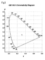
Fig. 2 is a diagram showing a spectral characteristic of a first embodiment; -
Fig. 3 is a diagram showing the reflected color of the first embodiment; -
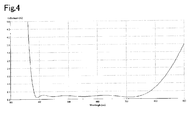
Fig. 4 is a diagram showing a spectral characteristic of a second embodiment; -
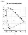
Fig. 5 is a diagram showing the reflected color of the second embodiment; -
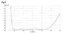
Fig. 6 is a diagram showing a spectral characteristic of a third embodiment; -
Fig. 7 is a diagram showing the reflected color of the third embodiment; -
Fig. 8 is a diagram showing a spectral characteristic of a first reference example (comparative example); -
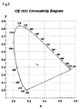
Fig. 9 is a diagram showing the reflected color of the first reference example (comparative example); -
Fig. 10 is a diagram showing a spectral characteristic of a second reference example (comparative example); and -
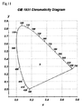
Fig. 11 is a diagram showing the reflected color of the second reference example (comparative example). - Examples of the invention will be described below. As shown in
Fig. 1 , reinforcement treatment intended to prevent cracking is performed on aglass substrate 10 in order to form a reinforcement layer 12. The substrate is not limited to the glass substrate such as a cover glass but may be an optical substrate made of a resin or metal or formed with a film or panel, or a mixture substrate made of glass and a resin or glass and a metal. - Antiglare (AG) treatment is performed on the reinforcement layer 12 in order to form an antiglare layer 14.
- On the antiglare layer 14, at least nine antireflection films are formed. For example, a reflected color adjustment low-reflectance antireflection film 16 (interference film) that includes nine layers made of Nb2O5, SiO2, Nb2O5, SiO2, Nb2O5, SiO2, Nb2O5, MgF2, and SiO2 respectively, and effects only a small change in a reflected color dependent on an incident angle is formed.
- A material to be made into the
antireflection film 16 is a high-refractive index material (Nb2O5, Ta2O5, TiO2, or ZrO2), a mixture material of any of these materials, or a low-refractive index material (SiO2 or MgF2). - A film formation apparatus adopts a vacuum deposition method, ionization-assisted deposition (IAD) film formation method, radiofrequency (RF) ion plating film formation method, or any of various sputtering methods.
- As for a reflected color, a* and b* values in the CIELAB color space meet -5<a*<5 and -5<b*<5 respectively (for example, a D65 white light source is used).
- Further, anti-fingerprint adhesion (AY) film treatment is performed on the
antireflection film 16 in order to form anantifouling layer 18. - For the
antifouling layer 18, a silicone-series substance such as alkylsilane or a fluorine-series substance having part of protons thereof replaced by fluorine is adopted. The molecules of the substances are so small that even when the substance is coated over an antireflection film, it hardly affects the optical characteristics of the antireflection film. Since the substances readily react on moisture, that is, cause hydrolysis or silylation reaction, a coating fluid capable of preventing the reaction should be produced. A substrate to be coated is coated according to a dip coating technique or the like so that an alkyl group or fluorine group reacts on the substrate while being oriented to the surface of the substrate, whereby the substance is cohered and fixed to the substrate to be coated. Accordingly, antifouling performance is exerted to the greatest extent, and cohesion to the substrate to be coated is upgraded. Eventually, abrasion durability is improved. Electrification can be avoided by devising a combination with the material of an underlying antireflection film. - Further, if the antireflection film of the surface of the substrate to be coated is subjected to activation treatment such as plasma cleaning prior to coating, cohesion is further upgraded. Eventually, abrasion durability is drastically improved.
- An antireflection film is formed on an optical surface of a substrate in order to minimize reflection of rays from an interface between the optical substrate and a medium.
- The refractive index n1 of a superficial layer that abuts on a medium is equal to or lower than 1.50 with respect to a design center wavelength λ0.
- Preferably, the
antireflection film 16 in the present invention satisfies conditions (1) to (3) below on the assumption that nh denotes a refractive index of a high-refractive index material, nl denotes a refractive index of a low-refractive index material, and Δn denotes a difference between the refractive indices nh and nl of adjoining layers. - (1) nh≥2.0
- (2) nh≤1.60
- (3) Δn≥0.30
- The above numerical limitation is not merely derived from the results of simulation. An actual prototype has demonstrated that the numerical values realize the most suitable low reflectance at a probability of 90% or more.
- Further preferably, the
antireflection film 16 in the present invention satisfies conditions below on the assumption that n1, n2, n3, n4, n5, n6, n7, n8, and n9 denote the refractive indices of nine layers stacked in that order from a medium side, and d1, d2, d3, d4, d5, d6, d7, d8, and d9 denote the optical film thicknesses of the layers stacked in that order from the medium side. - (a) n2≤1.40
- (b) n3=n5=n7=n9>n1=n4=n6=n8>n2
- (c) 0.0225λ0<d1<0.0525λ0
- (d) 0.1453λ0≤d2≤0.3389λO
- (e) 0.0733λ0≤d3≤0.1710λ0
- (f) 0.0307λ0≤d4≤0.0716λ0
- (g) 0.2096λ0≤d5≤0.4892λ0
- (h) 0.0315λ0≤d6≤0.0735λ0
- (i) 0.0810λ0≤d7≤0.1889λ0
- (j) 0.0798λ0≤d8<0.1863λ0
- (k) 0.0258λ0≤d9λ0.0602λ0
- The above wavelength ranges are not merely derived from the results of simulation. An actual prototype has demonstrated that the wavelength ranges realize the most suitable low reflectance at a probability ranging from 80% to 95%.
- Further preferably, the superficial layer and second layer of the
antireflection film 16 in the present invention contain at least one material to be selected from a group including silicon oxide and magnesium fluoride. - Further preferably, the
antireflection film 16 in the present invention is used for visible rays whose wavelengths range from 390 nm to 800 nm. - Further preferably, the spectral reflectance of the
antireflection film 16 in the present invention is equal to or lower than 1.0% with respect to a wavelength range from 390 nm to 800 nm, and equal to or lower than 0.5% with respect to a wavelength range from 400 nm to 780 nm. The numerical limitation is also such that the most suitable low reflectance is realized at a probability of 90% or more. - Further preferably, a* and b* values in the CIELAB color space expressing the reflected color of the
antireflection film 16 in the present invention meet -5<a*<5 and -5<b*<5 respectively (for example, a D65 white light source is used). - Now, three exemplary embodiments of the invention will be described below in comparison with two reference examples. The structures of cover glasses employed in the examples of the invention and the reference examples are identical to that shown in
Fig. 1 . - Referring to a first embodiment of the invention, as an
optical substrate 10, for example, a glass substrate exhibiting a refractive index of 1.52 was employed. - An
antireflection film 16 having nine layers as specified in Table 1 below was fabricated. Reinforcement treatment intended to prevent cracking was performed on theglass substrate 10, whereby a reinforcement layer was formed. - When the number of layers was equal to or smaller than eight, a wavelength band to be covered by the
antireflection film 16 was narrowed. Accordingly, a change in a reflected color dependent on an incident angle of incident light that comes from outside was increased. However, when the number of layers was nine, the change in a reflected color dependent on the incident angle was limited, and cohesion between film materials was upgraded. When the antireflection film in this first example was employed in portable telecommunications equipment such as a smartphone, a display section of the equipment became easy to see because it was unsusceptible to outside light and hardly glared. - The first layer of the
antireflection film 16 on a medium side thereof is the superficial layer. The superficial layer was made of silicon oxide. - The film material of the second layer was magnesium fluoride, the film material of the third, fifth, seventh, and ninth layers was niobium oxide, and the film material of the fourth, sixth, and eighth layers was silicon oxide.
- A design center wavelength λ0 was 480 nm.
- The first layer and the third to ninth layers on the medium side were formed by adopting an ion assisted method.
- The second layer was formed using a vacuum deposition method.
- More particularly, the first layer and the third to ninth layers were formed using an ion assisted apparatus in order to attain the optical film thicknesses listed in Table 1 with satisfactory reproducibility.
- Further, anti-fingerprint adhesion (AY) film treatment is performed on the
antireflection film 16, whereby an antifouling layer was formed. - The spectral characteristic and reflected color associated with the optical film thicknesses listed in Table 1 are as shown in
Fig. 2 andFig. 3 . - The optical substrate is adapted to, for example, a reinforcement glass for portable telecommunications equipment.
Table 1 Material Refractive index Optical film thickness Medium Air 1.00 - First layer SiO2 1.46 0.0375λ0 Second layer MgF2 1.39 0.2421λ0 Third layer Nb2O5 2.41 0.1222λ0 Fourth layer SiO2 1.46 0.0511λ0 Fifth layer Nb2O5 2.41 0.3494λ0 Sixth layer SiO2 1.46 0.0525λ0 Seventh layer Nb2O5 2.41 0.1349λ0 Eighth layer SiO2 1.46 0.1330λ0 Ninth layer Nb2O5 2.41 0.0430λ0 - Referring to a second embodiment of the invention, a substrate whose surface was subjected to antiglare treatment was adopted as a
glass substrate 10. Incidentally, reinforcement treatment intended to prevent cracking was performed on theglass substrate 10, whereby a reinforcement layer was formed. - An
antireflection film 16 having nine layers specified in Table 2 below was fabricated. - When the number of layers was equal to or smaller than eight, a wavelength band to be covered by the antireflection film was narrowed. Accordingly, a change in a reflected color dependent on an incident angle of incident light that comes from outside was increased. However, when the number of layers was nine, the change in a reflected color dependent on the incident angle was limited, and cohesion between film materials was upgraded. When the antireflection film of this second example was employed in portable telecommunications equipment such as a smartphone, a display section became easy to see because it was unsusceptible to outside light and hardly glared.
- The first layer of the
antireflection film 16 on a medium side thereof is the superficial layer. The superficial layer was made of silicon oxide. - The film material of the second layer was magnesium fluoride, the film material of the third, fifth, seventh, and ninth layers was niobium oxide, and the film material of the fourth, sixth, and eighth layers was silicon oxide.
- A design center wavelength λ0 was 480 nm.
- The first layer and the third to ninth layers on the medium side were formed by adopting an ion assisted method.
- The second layer was formed using a vacuum deposition method.
- More particularly, the first layer and the third to ninth layers were formed using an ion assisted apparatus in order to attain the optical film thicknesses listed in Table 2 below with satisfactory reproducibility.
- Further, anti-fingerprint adhesion (AY) film treatment was performed on the
antireflection film 16, whereby an antifouling layer was formed. - The optical substrate is adapted to a touch panel for personal computers or mobile devices or a cover glass for portable cellular phones.
- The spectral characteristic and reflected color associated with the optical film thicknesses listed in Table 2 are as shown in
Fig. 4 andFig. 5 .Table 2 Material Refractive index Optical film thickness Medium Air 1.00 - First layer SiO2 1.46 0.0375λ0 Second layer MgF2 1.39 0.2402λ0 Third layer Nb2O5 2.41 0.1232λ0 Fourth layer SiO2 1.46 0.0487λ0 Fifth layer Nb2O5 2.41 0.3503λ0 Sixth layer SiO2 1.46 0.0599λ0 Seventh layer Nb2O5 2.41 0.1177λ0 Eighth layer SiO2 1.46 0.1701λ0 Ninth layer Nb2O5 2.41 0.0303λ0 - Referring to a third embodiment of the invention, a substrate exhibiting a refractive index of 1.52 was adopted as a
glass substrate 10. - The surface of the
glass substrate 10 of the present example underwent neither antiglare treatment nor reinforcement treatment intended to prevent cracking. - An
antireflection film 16 having ten layers specified in Table 3 below was fabricated. - When the number of layers is equal to or smaller than eight, a wavelength band to be covered by the antireflection film was narrowed. A change in a reflected color dependent on an incident angle of incident light that comes from outside was increased. However, when the number of layers is ten, the change in a reflected color dependent on the incident angle was limited, and cohesion between film materials was upgraded. When the antireflection film of this third example was employed in portable telecommunications equipment such as a smartphone, a display section became easy to see because it was unsusceptible to outside light and hardly glared.
- The first layer of the
antireflection film 16 on a medium side thereof is the superficial layer. The superficial layer was made of silicon oxide. - The film material of the second layer was magnesium fluoride, the film material of the third, fifth, seventh, and ninth layers was niobium oxide, and the film material of the fourth, sixth, eighth, and tenth layers was silicon oxide.
- A design center wavelength λ0 was 480 nm.
- The first layer and the third to tenth layers on the medium side were formed by adopting an ion assisted method.
- The second layer was formed using a vacuum deposition method.
- More particularly, the first layer and the third to tenth layers were formed using an ion assisted apparatus in order to attain the optical film thicknesses listed in Table 3 with satisfactory reproducibility.
- Further, anti-fingerprint adhesion (AY) film treatment was performed on the
antireflection film 16, whereby an antifouling layer was formed. - The optical substrate is adapted to, for example, a cover glass for car navigation devices or an ordinary glass plate.
- The spectral characteristic and reflected color associated with the optical film thicknesses listed in Table 3 are as shown in
Fig. 6 andFig. 7 .Table 3 Material Refractive index Optical film thickness Medium Air 1.00 - First layer SiO2 1.46 0.0375λ0 Second layer MgF2 1.39 0.2419λ0 Third layer Nb2O5 2.41 0.1240λ0 Fourth layer SiO2 1.46 0.0498λ0 Fifth layer Nb2O5 2.41 0.3538λ0 Sixth layer SiO2 1.46 0.0579λ0 Seventh layer Nb2O5 2.41 0.1229λ0 Eighth layer SiO2 1.46 0.1531λ0 Ninth layer Nb2O5 2.41 0.0452λ0 Tenth layer SiO2 1.46 0.1228λ0 - Referring to a first reference example, a substrate exhibiting a refractive index of 1.52 was adopted as a
glass substrate 10. - An
antireflection film 16 having four layers specified in Table 4 below was fabricated. - Since the number of layers is four, about 60% of the most suitable reflectance is attained. Chromaticity can be satisfied. However, a wavelength band to be covered by the
antireflection film 16 was narrowed, and a change in a reflected color dependent on an incident angle of incident light that comes from outside was increased. - The first layer of the
antireflection film 16 on a medium side thereof is the superficial layer. The superficial layer was made of silicon oxide. - The film material of the second layer was magnesium fluoride, that of the third layer was ZrO2, and that of the fourth layer was Al2O3 .
- A design center wavelength λ0 was 510 nm.
- The first, third, and fourth layers on the medium side were formed by adopting an ion assisted method.
- The second layer was formed using a vacuum deposition method.
- More particularly, the first, third, and fourth layers were formed using an ion assisted apparatus in order to attain the optical film thicknesses listed in Table 4 with satisfactory reproducibility.
- Further, anti-fingerprint adhesion (AY) film treatment was performed on the antireflection film, whereby an antifouling layer was formed.
- The spectral characteristic and reflected color associated with the optical film thicknesses listed in Table 4 are as shown in
Fig. 8 andFig. 9 .Table 4 Material Refractive index Optical film thickness Medium Air 1.00 - First layer SiO2 1.46 0.0375λ0 Second layer MgF2 1.38 0.1994λ0 Third layer ZrO2 2.07 0.5068λ0 Fourth layer Al2O3 1.63 0.2763λ0 - Referring to a second reference example, a substrate exhibiting a refractive index of 1.52 was adopted as a
glass substrate 10. - An
antireflection film 16 having six layers specified in Table 5 below was fabricated. - Since the number of layers is six, about 80% of the most suitable reflectance is attained. Chromaticity can be satisfied. However, a wavelength band to be covered by the
antireflection film 16 was narrowed, and a change in a reflected color dependent on an incident angle of incident light that comes from outside was increased. - The first layer of the
antireflection film 16 on a medium side thereof is the superficial layer. The superficial layer was made of silicon oxide. - The film material of the second layer was magnesium fluoride, that of the third and fifth layers was ZrO2, that of the fourth layer was TiO2, and that of the sixth layer was Al2O3. A design center wavelength λ0 was 510 nm.
- The first layer and the third to sixth layers on the medium side were formed by adopting an ion assisted method.
- The second layer was formed using a vacuum deposition method.
- More particularly, the first layer and the third to sixth layers on the medium side were formed using an ion assisted apparatus in order to attain the optical film thicknesses listed in Table 5 with satisfactory reproducibility.
- Further, anti-fingerprint adhesion (AY) film treatment was performed on the antireflection film, whereby an antifouling layer was formed.
- The spectral characteristic and reflected color associated with the optical film thicknesses listed in
Fig. 5 are as shown inFig. 10 andFig. 11 .Table 5 Material Refractive index Optical film thickness Medium Air 1.00 - First layer SiO2 1.46 0.0375λ0 Second layer MgF2 1.39 0.2154λ0 Third layer ZrO2 2.06 0.2462λ0 Fourth layer TiO2 2.36 0.1597λ0 Fifth layer ZrO2 2.06 0.2290λ0 Sixth layer Al2O3 1.63 0.2436λ0
Claims (10)
- An optical substrate comprising:a tone-adjustment antireflection film (16); andan antifouling layer (18) formed on the antireflection film in order to minimize fingerprint adhesion, whereinthe antireflection film includes at least nine layers.
- The optical substrate according to claim 1, further comprising a reinforcement layer (12) intended to prevent cracking, wherein the tone-adjustment antireflection film (16) is formed on the reinforcement layer.
- The optical substrate according to claim 1, further comprising:a reinforcement layer intended to prevent cracking; andan antiglare layer formed on the reinforcement layer;wherein the a tone-adjustment antireflection film is formed on the antiglare layer.
- The optical substrate according to any one of claims 1 to 3, wherein:the antireflection film is made of a high-refractive index material of Nb2O5, Ta2O5, TiO2, or ZrO2, or a mixture material using any of these materials, and a low-refractive index material of SiO2 or MgF2; andassuming that nh denotes the refractive index of the high-refractive index material, nl denotes the refractive index of the low-refractive index material, and Δn denotes a difference between the refractive indices nh and nl of adjoining layers, the antireflection film satisfies the following conditions (1) to (3):(1) nh≥2.0(2) nl≤1.60(3) Δn≥0.30
- The optical substrate according to any one of claims 1 to 3, wherein:the antireflection film includes nine layers;assuming that n1, n2, n3, n4, n5, n6, n7, n8, and n9 denote the refractive indices of the nine layers beginning with a layer on an extremely medium side of the antireflection film, and d1, d2, d3, d4, d5, d6, d7, d8, and d9 denote the optical film thicknesses of the respective layers beginning with the layer on the extremely medium side, the antireflection film satisfies the following conditions:(a) n2≤1.40(b) n3=n5=n7=n9>n1=n4=n6=n8>n2(c) 0.0225λ0≤d1≤0.0525λ0(d) 0.1453λ0≤d2≤0.3389λ0(e) 0.0733λ0≤d3≤0.1710λ0(f) 0.0307λ0≤d4≤0.0716λ0(g) 0.2096λ0≤d5≤0.4892λ0(h) 0.0315λ0≤d6≤0.0735λ0(i) 0.0810λ0≤d7≤0.1889λ0(j) 0.0798λ0≤d8≤0.1863λ0(k) 0.0258λ0≤d9≤0.0602λ0
- The optical substrate according to any one of claims 1 to 5, wherein a superficial layer and a second layer of the antireflection film contain at least one material selected from a group including silicon oxide and magnesium fluoride.
- The optical substrate according to any one of claims 1 to 6, wherein the antireflection film is used for visible rays whose wavelengths range from 390 nm to 800 nm.
- The optical substrate according to any one of claims 1 to 7, wherein the spectral reflectance of the antireflection film is equal to or lower than 1.0% with respect to a wavelength range from 390 nm to 800 nm, and equal to or lower than 0.5% with respect to a wavelength range from 400 nm to 780 nm.
- The optical substrate according to any one of claims 1 to 8, wherein when a D65 white light source is used, a* and b* values in a CIELAB color space expressing the reflected color of an antireflection film employed meet -5<a*<5 and -5<b*<5 respectively.
- The optical substrate according to any one of claims 1 to 9, wherein the antifouling layer includes a water-repellent and oil-repellent film.
Applications Claiming Priority (1)
| Application Number | Priority Date | Filing Date | Title |
|---|---|---|---|
| JP2012018267A JP2013156523A (en) | 2012-01-31 | 2012-01-31 | Substrate |
Publications (1)
| Publication Number | Publication Date |
|---|---|
| EP2624020A1 true EP2624020A1 (en) | 2013-08-07 |
Family
ID=47263038
Family Applications (1)
| Application Number | Title | Priority Date | Filing Date |
|---|---|---|---|
| EP12188115.5A Withdrawn EP2624020A1 (en) | 2012-01-31 | 2012-10-11 | Optical substrate |
Country Status (4)
| Country | Link |
|---|---|
| US (1) | US8882280B2 (en) |
| EP (1) | EP2624020A1 (en) |
| JP (1) | JP2013156523A (en) |
| CN (1) | CN103226211B (en) |
Cited By (6)
| Publication number | Priority date | Publication date | Assignee | Title |
|---|---|---|---|---|
| CN104333629A (en) * | 2014-12-02 | 2015-02-04 | 张家港市德力特新材料有限公司 | Mobile phone screen glass |
| EP3518006A3 (en) * | 2018-01-30 | 2019-10-09 | Viavi Solutions Inc. | Optical device having optical and mechanical properties |
| EP3540478A3 (en) * | 2018-03-13 | 2019-12-18 | Viavi Solutions Inc. | Optical device including stack of optical layers with functional treatment |
| US11156753B2 (en) | 2017-12-18 | 2021-10-26 | Viavi Solutions Inc. | Optical filters |
| US12578519B2 (en) | 2020-03-05 | 2026-03-17 | Viavi Solutions Inc. | Optical coating for organic surface treatments |
| US12595549B2 (en) | 2016-06-13 | 2026-04-07 | Viavi Solutions Inc. | Optical filter including a high refractive index material |
Families Citing this family (54)
| Publication number | Priority date | Publication date | Assignee | Title |
|---|---|---|---|---|
| US9844898B2 (en) | 2011-09-30 | 2017-12-19 | Apple Inc. | Mirror feature in devices |
| JPWO2014034720A1 (en) * | 2012-08-31 | 2016-08-08 | 日本電気硝子株式会社 | Antiglare / antireflection member and method for producing the same |
| US9110230B2 (en) | 2013-05-07 | 2015-08-18 | Corning Incorporated | Scratch-resistant articles with retained optical properties |
| US9359261B2 (en) * | 2013-05-07 | 2016-06-07 | Corning Incorporated | Low-color scratch-resistant articles with a multilayer optical film |
| US9703011B2 (en) | 2013-05-07 | 2017-07-11 | Corning Incorporated | Scratch-resistant articles with a gradient layer |
| US9366784B2 (en) | 2013-05-07 | 2016-06-14 | Corning Incorporated | Low-color scratch-resistant articles with a multilayer optical film |
| US9684097B2 (en) | 2013-05-07 | 2017-06-20 | Corning Incorporated | Scratch-resistant articles with retained optical properties |
| CN110989319B (en) | 2013-06-09 | 2021-10-08 | 苹果公司 | Electronic watch |
| US9790126B2 (en) | 2013-09-05 | 2017-10-17 | Apple Inc. | Opaque color stack for electronic device |
| US9727178B2 (en) | 2013-09-05 | 2017-08-08 | Apple Inc. | Opaque white coating with non-conductive mirror |
| US9629271B1 (en) | 2013-09-30 | 2017-04-18 | Apple Inc. | Laser texturing of a surface |
| CN103950248A (en) * | 2014-04-21 | 2014-07-30 | 深圳市三鑫精美特玻璃有限公司 | Anti-dazzle and antireflection (AR) glass capable of resisting fingerprint, and processing method thereof |
| US9335444B2 (en) | 2014-05-12 | 2016-05-10 | Corning Incorporated | Durable and scratch-resistant anti-reflective articles |
| US11267973B2 (en) | 2014-05-12 | 2022-03-08 | Corning Incorporated | Durable anti-reflective articles |
| WO2016010009A1 (en) | 2014-07-16 | 2016-01-21 | 旭硝子株式会社 | Cover glass |
| US9790593B2 (en) * | 2014-08-01 | 2017-10-17 | Corning Incorporated | Scratch-resistant materials and articles including the same |
| JP6458804B2 (en) * | 2014-08-04 | 2019-01-30 | Agc株式会社 | Translucent structure |
| CN204694870U (en) * | 2014-08-11 | 2015-10-07 | 深圳市康视佳网络科技发展有限公司 | A kind of Multifunctional lens |
| CN105445820A (en) * | 2014-08-21 | 2016-03-30 | 宸鸿科技(厦门)有限公司 | Optical film assembly |
| WO2016035710A1 (en) * | 2014-09-02 | 2016-03-10 | コニカミノルタ株式会社 | Prism unit and projector |
| CN104503009B (en) * | 2014-12-09 | 2016-03-23 | 成都摩卡科技有限责任公司 | A kind of anti-dazzle solar film and preparation method thereof |
| DE102015100091A1 (en) * | 2015-01-07 | 2016-07-07 | Rodenstock Gmbh | Layer system and optical element with a layer system |
| DE112016003903T5 (en) | 2015-08-31 | 2018-05-30 | Asahi Glass Company, Limited | Translucent structure, process for its preparation and object |
| JP2018536177A (en) | 2015-09-14 | 2018-12-06 | コーニング インコーポレイテッド | High light transmittance and scratch resistant anti-reflective article |
| JP6549458B2 (en) | 2015-09-30 | 2019-07-24 | 株式会社トプコン | Antireflection film, optical element, and ophthalmologic apparatus |
| JP2017110979A (en) * | 2015-12-15 | 2017-06-22 | 株式会社ミツトヨ | Measuring instrument |
| WO2017135261A1 (en) * | 2016-02-01 | 2017-08-10 | 旭硝子株式会社 | Translucent structure |
| CN105857209A (en) * | 2016-05-04 | 2016-08-17 | 科世达(上海)管理有限公司 | Automobile interior part and manufacturing method thereof |
| EP3242150B1 (en) * | 2016-05-04 | 2019-01-02 | Essilor International | Optical article comprising an antireflective coating with a high reflection in the near infrared region (nir) |
| CN105891914B (en) * | 2016-06-04 | 2017-12-15 | 浙江星星科技股份有限公司 | A kind of windows be protected panel with AG+AR+AF plated films |
| CN106086791B (en) * | 2016-06-04 | 2018-08-10 | 浙江星星科技股份有限公司 | A kind of manufacturing method of the windows be protected panel with AG+AR+AF plated films |
| CN108349296B (en) | 2016-09-06 | 2019-11-05 | 苹果公司 | Laser bleach marking of anodized surfaces |
| JP6780619B2 (en) * | 2016-11-11 | 2020-11-04 | Agc株式会社 | Substrate with low reflective film and its manufacturing method |
| US10877181B2 (en) * | 2016-11-11 | 2020-12-29 | AGC Inc. | Substrate with low-reflection property and manufacturing method thereof |
| KR101926960B1 (en) * | 2017-02-10 | 2018-12-07 | 주식회사 케이씨씨 | Low Reflection Coating Glass |
| CN106918851A (en) * | 2017-04-26 | 2017-07-04 | 福建福光光电科技有限公司 | A kind of superhard optical glass film layer of hydrophobic oleophobic anti-soil |
| JP6881172B2 (en) * | 2017-09-13 | 2021-06-02 | Agc株式会社 | Transparent substrate with antireflection film and display device using it |
| CN107731874A (en) * | 2017-10-18 | 2018-02-23 | 曾胜 | A kind of anti-dazzle light solution of novel capacitance screen |
| JP7310791B2 (en) * | 2018-02-16 | 2023-07-19 | Agc株式会社 | Cover glass and in-cell liquid crystal display device |
| EP3759530A1 (en) * | 2018-03-02 | 2021-01-06 | Corning Incorporated | Anti-reflective coatings and articles and methods of forming the same |
| US10919326B2 (en) | 2018-07-03 | 2021-02-16 | Apple Inc. | Controlled ablation and surface modification for marking an electronic device |
| CN114085038A (en) | 2018-08-17 | 2022-02-25 | 康宁股份有限公司 | Inorganic oxide articles with thin durable antireflective structures |
| DE102018122444B4 (en) * | 2018-09-13 | 2025-12-18 | Rodenstock Gmbh | Optical element with a stack of layer packages |
| US11200385B2 (en) | 2018-09-27 | 2021-12-14 | Apple Inc. | Electronic card having an electronic interface |
| US11571766B2 (en) | 2018-12-10 | 2023-02-07 | Apple Inc. | Laser marking of an electronic device through a cover |
| US11650361B2 (en) | 2018-12-27 | 2023-05-16 | Viavi Solutions Inc. | Optical filter |
| US11299421B2 (en) | 2019-05-13 | 2022-04-12 | Apple Inc. | Electronic device enclosure with a glass member having an internal encoded marking |
| CN110415610A (en) * | 2019-07-22 | 2019-11-05 | 安徽华米信息科技有限公司 | Display panel and its manufacturing method, display device |
| US10830930B1 (en) * | 2019-09-09 | 2020-11-10 | Apple Inc. | Antireflective infrared cut filter coatings for electronic devices |
| CN110976249A (en) * | 2019-12-20 | 2020-04-10 | 深圳市佰瑞兴实业有限公司 | Surface treatment process of glass display panel |
| US12386101B2 (en) | 2020-07-09 | 2025-08-12 | Corning Incorporated | Textured region of a substrate to reduce specular reflectance incorporating surface features with an elliptical perimeter or segments thereof, and method of making the same |
| CN112209632A (en) * | 2020-09-18 | 2021-01-12 | 苏州胜利精密制造科技股份有限公司 | Glass cover plate of blue touch panel and preparation method |
| JP7042895B1 (en) * | 2020-11-27 | 2022-03-28 | デクセリアルズ株式会社 | Optical laminates and articles |
| CN116589194B (en) * | 2021-01-29 | 2025-10-21 | 重庆鑫景特种玻璃有限公司 | A glass-ceramic display screen and its manufacturing method |
Citations (4)
| Publication number | Priority date | Publication date | Assignee | Title |
|---|---|---|---|---|
| JPH0478520B2 (en) | 1984-04-03 | 1992-12-11 | Fujitsu Kk | |
| FR2846753A1 (en) * | 2002-11-06 | 2004-05-07 | Pentax Corp | ANTI-REFLECTIVE GLASSES OF GLASSES AND METHOD FOR THE PRODUCTION THEREOF |
| JP3710721B2 (en) | 2001-04-25 | 2005-10-26 | 三井化学株式会社 | Display filter manufacturing method |
| JP2011039218A (en) * | 2009-08-10 | 2011-02-24 | Seiko Epson Corp | Method for producing optical article |
Family Cites Families (11)
| Publication number | Priority date | Publication date | Assignee | Title |
|---|---|---|---|---|
| JPH078520B2 (en) | 1991-02-28 | 1995-02-01 | 株式会社日本製鋼所 | Automatic confirmation method for color change of injection molded products |
| JPH10206603A (en) * | 1997-01-20 | 1998-08-07 | Dainippon Printing Co Ltd | Antireflection film and method for producing the same |
| JP3311720B2 (en) * | 1999-01-22 | 2002-08-05 | 三井化学株式会社 | Display filter |
| JP4078520B2 (en) | 2002-01-21 | 2008-04-23 | 旭硝子株式会社 | Manufacturing method of filter with antireflection function for display device |
| US7695781B2 (en) * | 2004-02-16 | 2010-04-13 | Fujifilm Corporation | Antireflective film, polarizing plate including the same, image display unit including the same and method for producing antireflective film |
| JP2006126233A (en) * | 2004-10-26 | 2006-05-18 | Seiko Epson Corp | Eyeglass lens with anti-reflection coating |
| US7939576B2 (en) * | 2005-11-25 | 2011-05-10 | Fujifilm Corporation | Antireflection film, process of producing the same, and polarizing plate and display device including the same |
| JP2009008901A (en) * | 2007-06-28 | 2009-01-15 | Nikon Corp | Antireflection film, optical element and optical system |
| JP5163231B2 (en) * | 2008-03-31 | 2013-03-13 | 日油株式会社 | Anti-reflective material and electronic image display device including the same |
| CN101571602A (en) * | 2008-04-29 | 2009-11-04 | 智盛全球股份有限公司 | Anti-reflection coating structure for increasing blue light transmittance and manufacturing method thereof |
| JP2010231171A (en) * | 2009-03-04 | 2010-10-14 | Seiko Epson Corp | Optical article and manufacturing method thereof |
-
2012
- 2012-01-31 JP JP2012018267A patent/JP2013156523A/en active Pending
- 2012-09-14 CN CN201210342252.3A patent/CN103226211B/en active Active
- 2012-10-09 US US13/647,875 patent/US8882280B2/en active Active
- 2012-10-11 EP EP12188115.5A patent/EP2624020A1/en not_active Withdrawn
Patent Citations (4)
| Publication number | Priority date | Publication date | Assignee | Title |
|---|---|---|---|---|
| JPH0478520B2 (en) | 1984-04-03 | 1992-12-11 | Fujitsu Kk | |
| JP3710721B2 (en) | 2001-04-25 | 2005-10-26 | 三井化学株式会社 | Display filter manufacturing method |
| FR2846753A1 (en) * | 2002-11-06 | 2004-05-07 | Pentax Corp | ANTI-REFLECTIVE GLASSES OF GLASSES AND METHOD FOR THE PRODUCTION THEREOF |
| JP2011039218A (en) * | 2009-08-10 | 2011-02-24 | Seiko Epson Corp | Method for producing optical article |
Cited By (8)
| Publication number | Priority date | Publication date | Assignee | Title |
|---|---|---|---|---|
| CN104333629A (en) * | 2014-12-02 | 2015-02-04 | 张家港市德力特新材料有限公司 | Mobile phone screen glass |
| US12595549B2 (en) | 2016-06-13 | 2026-04-07 | Viavi Solutions Inc. | Optical filter including a high refractive index material |
| US11156753B2 (en) | 2017-12-18 | 2021-10-26 | Viavi Solutions Inc. | Optical filters |
| EP3518006A3 (en) * | 2018-01-30 | 2019-10-09 | Viavi Solutions Inc. | Optical device having optical and mechanical properties |
| US11360242B2 (en) | 2018-01-30 | 2022-06-14 | Viavi Solutions Inc. | Optical device having optical and mechanical properties |
| US12174342B2 (en) | 2018-01-30 | 2024-12-24 | Viavi Solutions Inc. | Optical device having optical and mechanical properties |
| EP3540478A3 (en) * | 2018-03-13 | 2019-12-18 | Viavi Solutions Inc. | Optical device including stack of optical layers with functional treatment |
| US12578519B2 (en) | 2020-03-05 | 2026-03-17 | Viavi Solutions Inc. | Optical coating for organic surface treatments |
Also Published As
| Publication number | Publication date |
|---|---|
| US20130271836A1 (en) | 2013-10-17 |
| CN103226211A (en) | 2013-07-31 |
| US8882280B2 (en) | 2014-11-11 |
| CN103226211B (en) | 2015-05-13 |
| JP2013156523A (en) | 2013-08-15 |
Similar Documents
| Publication | Publication Date | Title |
|---|---|---|
| US8882280B2 (en) | Optical substrate | |
| CN113728251B (en) | Optical laminate and article | |
| TWI460742B (en) | Transparent conductive film | |
| TWI600918B (en) | Optical film | |
| KR102850311B1 (en) | Antireflection film and image display device | |
| US9103970B2 (en) | Optical layered body, method for producing optical layered body, polarizer, and image display device | |
| US20120181063A1 (en) | Transparent conductive film and touch panel | |
| TWI467215B (en) | Hard-coated antiglare film, polarizing plate and image display including the same, and method for producing the same | |
| JP2011081219A (en) | Hard-coated antiglare film, and polarizing plate and image display including the same | |
| JPH11258405A (en) | Anti-reflection film | |
| JP5160329B2 (en) | Transparent conductive film and touch panel | |
| CN113039463A (en) | Anti-glare film, method for producing anti-glare film, optical member, and image display device | |
| TWI901817B (en) | Optical laminate and article | |
| JP2002082205A (en) | Antireflection film, optical function film and display device using the same | |
| JP6526380B2 (en) | Display with touch panel | |
| EP4524619A1 (en) | Optical multilayer body and article | |
| KR101565855B1 (en) | Transparent conductive optical sheet having high invisibility of pattern | |
| JP2009222851A (en) | Conductive antireflection film | |
| KR102341198B1 (en) | Hard coating film and image display device using the same | |
| KR102548449B1 (en) | Window for display device | |
| KR20190049277A (en) | Optical antireflection film and manufacturing method of the same | |
| JP2015208987A (en) | Color tone correction film and transparent conductive film using the same | |
| TWI922207B (en) | Optical laminate and article | |
| JP6136376B2 (en) | Color tone correction film and transparent conductive film using the same | |
| KR20240171270A (en) | Film structure with anti-reflection, anti-glare and anti-fingerprint property |
Legal Events
| Date | Code | Title | Description |
|---|---|---|---|
| PUAI | Public reference made under article 153(3) epc to a published international application that has entered the european phase |
Free format text: ORIGINAL CODE: 0009012 |
|
| AK | Designated contracting states |
Kind code of ref document: A1 Designated state(s): AL AT BE BG CH CY CZ DE DK EE ES FI FR GB GR HR HU IE IS IT LI LT LU LV MC MK MT NL NO PL PT RO RS SE SI SK SM TR |
|
| AX | Request for extension of the european patent |
Extension state: BA ME |
|
| 17P | Request for examination filed |
Effective date: 20140127 |
|
| RBV | Designated contracting states (corrected) |
Designated state(s): AL AT BE BG CH CY CZ DE DK EE ES FI FR GB GR HR HU IE IS IT LI LT LU LV MC MK MT NL NO PL PT RO RS SE SI SK SM TR |
|
| 17Q | First examination report despatched |
Effective date: 20161130 |
|
| STAA | Information on the status of an ep patent application or granted ep patent |
Free format text: STATUS: THE APPLICATION IS DEEMED TO BE WITHDRAWN |
|
| 18D | Application deemed to be withdrawn |
Effective date: 20170411 |