EP2590261A2 - Leistungseffiziente Mehrfachmodus-Transceiver-Synthesizer-Konfigurationen - Google Patents
Leistungseffiziente Mehrfachmodus-Transceiver-Synthesizer-Konfigurationen Download PDFInfo
- Publication number
- EP2590261A2 EP2590261A2 EP12006125.4A EP12006125A EP2590261A2 EP 2590261 A2 EP2590261 A2 EP 2590261A2 EP 12006125 A EP12006125 A EP 12006125A EP 2590261 A2 EP2590261 A2 EP 2590261A2
- Authority
- EP
- European Patent Office
- Prior art keywords
- transceiver
- signal
- receive
- transmit
- mode
- Prior art date
- Legal status (The legal status is an assumption and is not a legal conclusion. Google has not performed a legal analysis and makes no representation as to the accuracy of the status listed.)
- Withdrawn
Links
Images


Classifications
-
- H—ELECTRICITY
- H04—ELECTRIC COMMUNICATION TECHNIQUE
- H04B—TRANSMISSION
- H04B1/00—Details of transmission systems, not covered by a single one of groups H04B3/00 - H04B13/00; Details of transmission systems not characterised by the medium used for transmission
- H04B1/38—Transceivers, i.e. devices in which transmitter and receiver form a structural unit and in which at least one part is used for functions of transmitting and receiving
- H04B1/40—Circuits
- H04B1/403—Circuits using the same oscillator for generating both the transmitter frequency and the receiver local oscillator frequency
-
- H—ELECTRICITY
- H04—ELECTRIC COMMUNICATION TECHNIQUE
- H04J—MULTIPLEX COMMUNICATION
- H04J4/00—Combined time-division and frequency-division multiplex systems
Definitions
- the field of the invention relates generally to wireless communication transceivers.
- the transceiver support both frequency division duplexing (FDD) and time division duplexing (TDD) communication technologies.
- FDD mode transmit and receive functions are performed by the transceiver, on different carrier frequencies, simultaneously.
- TDD mode transmit and receive functions are performed by the transceiver at respective non-overlapping time slots, on the same or different frequencies.
- At least two synthesizers and two local oscillator (LO) signal generation sections are used, in order to simultaneously generate and deliver high-precision TX and RX LO signals to the TX and RX mixers, respectively.
- LO local oscillator
- a common mode of operation includes selectively powering up/down the RX and TX synthesizers (and associated LO signal generation sections) as needed. For example, the RX synthesizer is powered up during receive time slots and powered down during transmit time slots, and the TX synthesizer is powered up during transmit time slots and powered down during receive time slots.
- this mode of operation requires very frequent powering up/down of the RX and TX synthesizers, resulting in several significant drawbacks and reduced power savings.
- a transceiver comprises:
- the transmit portion is configured to be powered down during the TDD mode of the transceiver.
- a frequency of the first LO signal corresponds to a transmit carrier frequency of the transceiver during the transmit time slot and to a receive carrier frequency of the transceiver during the receive time slot.
- the switching structure comprises a demultiplexer, the demultiplexer configured to receive the first LO signal and to couple the first LO signal to the receive mixer during the receive time slot and to the transmit mixer during the transmit time slot.
- the transmit synthesizer is configured to generate a second clock signal
- the transmit LO signal generation section is configured to generate a second LO signal from the second clock signal.
- the switching structure is configured to couple, simultaneously, the first LO signal to the receive mixer and the second LO signal to the transmit mixer.
- the switching structure further comprises a multiplexer, the multiplexer configured to receive the first LO signal and the second LO signal and to couple the first LO signal to the transmit mixer in the TDD mode of the transceiver and to couple the second LO signal to the transmit mixer in the FDD mode of the transceiver.
- both the transmit portion and the receive portion are configured to be powered on during the FDD mode of the transceiver.
- a transceiver comprises:
- the receive portion is configured to be powered down during the TDD mode of the transceiver.
- the switching structure comprises a demultiplexer, the demultiplexer configured to receive the first LO signal and to couple the first LO signal to the receive mixer during the receive time slot and to the transmit mixer during the transmit time slot.
- the receive synthesizer is configured to generate a second clock signal
- the receive LO signal generation section is configured to generate a second LO signal from the second clock signal.
- the switching structure is configured to couple, simultaneously, the first LO signal to the transmit mixer and the second LO signal to the receive mixer.
- the switching structure further comprises a multiplexer, the multiplexer configured to receive the first LO signal and the second LO signal and to couple the first LO signal to the receive mixer in the TDD mode of the transceiver and to couple the second LO signal to the receive mixer in the FDD mode of the transceiver.
- both the transmit portion and the receive portion are configured to be powered on during the FDD mode of the transceiver.
- a transceiver comprises:
- the transceiver further comprises:
- the LO signal generation section is configured, during the transmit time slot, to generate a first LO signal from the first clock signal and to provide the first LO signal to the transmit mixer, and wherein the auxiliary LO signal generation section is configured, during the receive time slot, to generate a second LO signal from the first clock signal and to provide the second LO signal to the receive mixer.
- the LO signal generation section is configured, during the receive time slot, to generate a first LO signal from the first clock signal and to provide the first LO signal to the receiver mixer, and wherein the auxiliary LO signal generation section is configured, during the transmit time slot, to generate a second LO signal from the first clock signal and to provide the second LO signal to the transmit mixer.
- the synthesizer and the LO signal generation section are part of the transmit portion, and wherein the receiver portion is configured to be powered down during the TDD mode of the transceiver.
- the synthesizer and the LO signal generation section are part of the receive portion, and wherein the transmit portion is configured to be powered down during the TDD mode of the transceiver.
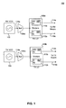
- FIG. 1 illustrates an example frequency division duplexing (FDD) transceiver section.
- FDD frequency division duplexing
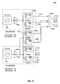
- FIG. 2 illustrates an example FDD transceiver section modified for dual FDD-time division duplexing (TDD) operation.
- TDD time division duplexing
- FIG. 3 illustrates another example FDD transceiver section modified for dual FDD-TDD operation.
- FIG. 4 illustrates another example FDD transceiver section modified for dual FDD-TDD operation.
- FIG. 5 illustrates another example FDD transceiver section modified for dual FDD-TDD operation.
- FIG. 1 illustrates an example frequency division duplexing (FDD) transceiver section 100.
- Example FDD transceiver section 100 is provided for the purpose of illustration and is not limiting. As would be understood by a person of skill in the art based on the teachings herein, section 100 may have a different architecture or implementation details than shown in FIG. 1 .
- example FDD transceiver section 100 includes a receive (RX) portion and a transmit (TX) portion.
- the RX portion includes a RX synthesizer 102, a buffer 106a, and a RX local oscillator (LO) signal generation section 108a.
- the TX portion includes a TX synthesizer 104, a buffer 106b, and a TX LO signal generation section 108b.
- RX synthesizer 102 and TX synthesizer 104 may each include a voltage controlled oscillator (VCO).
- VCO voltage controlled oscillator
- RX synthesizer 102 and TX synthesizer 104 may each also include a phase locked loop (PLL) (not shown in FIG. 1 ), for example, which controls the VCO to generate a VCO output signal 118.
- PLL phase locked loop
- VCO output signal 118 is fed into buffer 106, before being provided to RX/TX LO signal generation section 108.
- RX and TX LO signal generation sections 108a and 108b may include one or more dividers as needed.
- RX LO signal generation section 108a includes dividers 110a and 112a.
- Dividers 110a and 112a can be configured to generate RX LO signals 114a and 116a, respectively, which are provided to the RX mixers of the FDD transceiver.
- TX LO signal generation section 108b includes dividers 110b and 112b.
- Dividers 110b and 112b can be configured to generate TX LO signals 114b and 116b, respectively, which are provided to the TX mixers of the FDD transceiver.
- RX/TX LO signals 114 and 116 may be single-ended or differential in-phase and quadrature phase (IQ) signals, for example.
- dividers 110 and 112 in RX/TX LO signal generation sections 108 are active at any given time, to generate a RX/TX LO signal 114 or 116. Accordingly, a power up/down function may be implemented to power up/down dividers 110 and 112, as needed, in RX/TX LO signal generation sections 108.
- RX and TX LO signal generation sections 108a and 108b may implement different LO signal generation schemes than shown in FIG. 1 , including different numbers of dividers and/or divider ratios, for example.
- transmit and receive functions are performed by the transceiver, on different carrier frequencies, simultaneously. Therefore, at least two synthesizers and two LO signal generation sections (as in example FDD transceiver section 100) are needed in order to simultaneously generate and deliver high-precision TX and RX LO signals to the TX and RX mixers.
- both the RX and TX portions need to be maintained ON at the same time in FDD mode. This includes maintaining both RX and TX synthesizers 102 and 104 and RX and TX LO signal generation sections 108a and 108b powered on at the same time.
- the transceiver support time division duplexing (TDD) communication technologies in addition to FDD communication technologies.
- TDD time division duplexing
- transmit and receive functions are performed by the transceiver at respective non-overlapping time slots, on the same or different frequencies.
- a FDD transceiver having a section like example section 100 can be configured to support TDD because, at any time in TDD mode, at most one synthesizer and one LO signal generation section is needed.
- a first configuration both the RX and TX portions of FDD transceiver section 100 are maintained ON at all time.
- receive time slots RX LO signal 114a/116a is used, and TX LO signal 114b/116b is discarded.
- TX LO signal 114b/116b is used, and RX LO signal 114a/116a is discarded.
- this first configuration is wasteful in terms of power consumption and duty cycle. It may also be sub-optimal for transitions between RX/TX mode due to the fact that advanced 4G-TDD standards require extremely fast transitions between these two modes.
- the RX and TX portions of FDD transceiver section 100 are selectively powered up/down as needed.
- the RX portion is powered up during receive time slots and powered down during transmit time slots
- the TX portion is powered up during transmit time slots and powered down during receive time slots.
- transmit/receive transition time allowed between slots may be too short (e.g., 12.5 microseconds) for the RX/TX portion of FDD transceiver section 100 to reach DC-state settling and/or required output frequency tolerance.
- capacitors are used to filter out low frequency noise. These capacitors, which are slow to fully charge/discharge, cause the RX/TX synthesizer to have slow DC-state settling compared to TDD slot times. As a result of having slow DC-state settling, portions of the RX/TX synthesizer may never be able to completely power-down within a time slot.
- the synthesizer's PLL may be only partially off when it is time to power it up again at the beginning of the next time slot. As such, potential power savings of this second configuration are not fully achieved in practice. Further, slow DC-state settling also means that the synthesizer may have to operate (i.e., generate an operational output) under transient conditions. This is especially undesirable in the case of synthesizers with low-voltage VCOs, which are highly sensitive to supply voltage settling problems.
- the frequent powering up/down of the RX and TX portions in this second configuration may also cause undesirable transient phenomena.
- the RX/TX synthesizer's PLL and VCO typically experience undesired device characteristics changes during power up, until DC-state settling is reached. These device characteristics changes may include fluctuations in VCO gain curves (e.g., due to cold-to-hot transitions) and current mismatches in charge pump circuits used in the PLLs, both of which may cause undesired spurs in the VCO output signal.
- frequent calibration of circuitry is also needed in this second configuration. For example, typically, the RX/TX synthesizer's VCO needs to be calibrated (in order to operate in the most favorable region of operation) after each power-up.
- the frequent powering up/down of the RX and TX synthesizers also makes infeasible the use of a switching regulator-based power supply (which is desired for its very high power efficiency) to power up the transceiver.
- switching regulators have slow settling following load changes, which reduces their power efficiency. Frequent powering up/down of the RX and TX synthesizers forces the switching regulator to operate a vast proportion of the time under varying load conditions, significantly lowering its power efficiency.
- Embodiments of the present disclosure provide power-efficient TDD mode configurations of FDD transceivers.
- Embodiments avoid time slotted operation of the RX and TX synthesizers, thereby avoiding the above described drawbacks of operation under transient conditions, frequent calibration, and reduced power supply efficiency.
- a single synthesizer is used to enable TDD operation, thereby reducing power consumption and calibration requirements by approximately 50%.
- the single synthesizer may be maintained ON at all times, thus allowing the power supply's switching regulator to operate with substantially constant load conditions.
- FIG. 2 illustrates an example FDD transceiver section 200 modified for dual FDD-TDD operation.
- Example FDD transceiver section 200 is provided for the purpose of illustration and is not limiting.
- example transceiver section 200 also includes an RX portion and a TX portion.
- the RX portion includes RX synthesizer 102, buffer 106a, and RX LO signal generation section 108a.
- the TX portion includes TX synthesizer 104, buffer 106b, and TX LO signal generation section 108b.
- transceiver section 200 includes de-multiplexers 202a-b and multiplexers 204a-b.
- De-multiplexers 202a and 202b are placed at the outputs of RX LO signal generation section 108a, so as to receive, respectively, RX LO signals 114a and 116a.
- the transceiver mode i.e., FDD mode vs.
- de-multiplexers 202a and 202b selectively couple, respectively, RX LO signals 114a and 116a either to the RX mixers (via signals 206a and 206b, respectively) or to multiplexers 204a and 204b (via signals 208a and 208b, respectively).
- Multiplexers 204a and 204b are placed at the outputs of TX LO signal generation section 108b, so as to receive, respectively, TX LO signals 114b and 116b.
- multiplexers 204a and 204b receive, respectively, signals 208a and 208b from de-multiplexers 202a and 202b.
- de-multiplexers 202a and 202b receive signals 208a and 208b from de-multiplexers 202a and 202b.
- multiplexers 204a and 204b selectively couple, respectively, either signals 114b/116b or signals 208a/208b to the TX mixers (via signals 210a and 210b, respectively).
- both the RX and TX portions of FDD transceiver section 200 are powered on, in order to enable simultaneous transmission and reception by the transceiver.
- de-multiplexers 202a-b are configured to couple, respectively, RX LO signals 114a and 116a to the RX mixers via signals 206a and 206b, respectively.
- Signals 208a-b thus remain inactive.
- Multiplexers 204a-b are configured to couple, respectively, TX LO signals 114b and 116b to the TX mixers via signals 210a and 210b, respectively.
- de-multiplexers 202a-b are configured to couple, respectively, RX LO signals 114a and 116a to the RX mixers via signals 206a and 206b, respectively.
- the RX portion of FDD transceiver section 200 is configured to produce TX LO signals 212a-b.
- TX LO signals 212a-b may be identical to or different from RX LO signals 114a and 116b, depending on whether transmit and receive functions are performed on same or different carrier frequencies in TDD mode.
- De-multiplexers 202a-b are configured to couple, respectively, TX LO signals 212a and 212b to multiplexers 204a and 204b, via signals 208a and 208b.
- Multiplexers 204a and 204b in turn couple, respectively, signals 208a and 208b to the TX mixers, via signals 210a and 210b.
- the RX portion of FDD transceiver section 200 active in TDD mode, significant power savings can be achieved.
- the RX portion is maintained powered on or is only turned off infrequently in TDD mode.
- the PLL of synthesizer 102 of the RX portion is characterized by fast settling performance, by virtue of its implementation of embodiments described in U.S. Patent Application No. 13/356,137, filed January 23, 2012 , entitled “Apparatus and Method for Fast Phase Locked Loop (PLL) Settling for Cellular Time-Division Duplex (TDD) Communications Systems,” which is incorporated herein by reference in its entirety. This reduces the negative effects of turning on/off the RX portion, as discussed above.
- FIG. 3 illustrates another example FDD transceiver section 300 modified for dual FDD-TDD operation.
- Example FDD transceiver section 300 is provided for the purpose of illustration and is not limiting.
- Example transceiver section 300 implements a reverse configuration relative to example transceiver section 200 described above in FIG. 2 .
- de-multiplexers 202a and 202b of transceiver section 200 are replaced, respectively, with multiplexers 304a and 304b at the outputs of RX LO signal generation section 108a in transceiver section 300.
- Multiplexers 204a and 204b of transceiver section 200 are replaced, respectively, with de-multiplexers 302a and 302b at the outputs of TX LO signal generation section 108b in transceiver section 300.
- transceiver section 300 operates as described above with respect to transceiver section 200, with de-multiplexers 302a-b configured to operate like de-multiplexers 202a-b and multiplexers 304a-b configured to operate like multiplexers 204a-b.
- de-multiplexers 302a-b are configured to couple, respectively, TX LO signals 114b and 116b to the TX mixers via signals 306a and 306b, respectively.
- the TX portion of FDD transceiver section 300 is configured to produce RX LO signals 312a-b.
- RX LO signals 312a-b may be identical to or different from TX LO signals 114b and 116b, depending on whether transmit and receive functions are performed on same or different carrier frequencies in TDD mode.
- De-multiplexers 302a-b are configured to couple, respectively, RX LO signals 312a and 312b to multiplexers 304a and 304b, via signals 308a and 308b.
- Multiplexers 304a and 304b in turn couple, respectively, signals 308a and 308b to the RX mixers, via signals 310a and 310b.
- the TX portion of FDD transceiver section 300 active in TDD mode, significant power savings can be achieved.
- the TX portion is maintained powered on or is only turned off infrequently in TDD mode.
- the PLL of synthesizer 104 of the TX portion is characterized by fast settling performance, by virtue of its implementation of embodiments described in U.S. Patent Application No. 13/356,137, filed January 23, 2012 , entitled “Apparatus and Method for Fast Phase Locked Loop (PLL) Settling for Cellular Time-Division Duplex (TDD) Communications Systems," which is incorporated herein by reference in its entirety. This reduces the negative effects of turning on/off the TX portion, as discussed above.
- example transceiver section 200 may be more favorable than example transceiver section 300, or vice versa.
- Some of the considerations in selecting between the two example sections include, for example, the respective power efficiencies of the TX and RX portions and the desired TDD transmit/receive carrier frequencies.
- the RX synthesizer may be designed to support higher frequency ranges than the TX synthesizer.
- either transceiver section 200 or transceiver section 300 may be more suitable.
- FIG. 4 illustrates another example FDD transceiver section 400 modified for dual FDD-TDD operation.
- Example FDD transceiver section 400 is provided for the purpose of illustration and is not limiting.
- Example transceiver section 400 implements a combination of the functionalities of example transceiver sections 200 and 300.
- De-multiplexers 202a-b are placed at the outputs of RX LO signal generation section 108a, but are not shown in FIG. 4 for the ease of illustration.
- De-multiplexers 302a-b are placed at the outputs of TX LO signal generation section 108b.
- de-multiplexers 202a-b followed by multiplexers 304a-b couple, respectively, RX LO signals 114a and 116a to the RX mixers, via signals 310a and 310b.
- de-multiplexers 302a-b followed by multiplexers 204a-b couple, respectively, TX LO signals 114b and 116b to the TX mixers, via signals 210a and 210b.
- either one of the RX portion and the TX portion of FDD transceiver section 400 is turned ON, and the other one is turned OFF. Selection between the two configurations can be made on the fly.
- the RX portion is ON, multiplexers 204a-b are active and transceiver section 400 operates like example transceiver section 200 in TDD mode.
- the TX portion is ON, multiplexers 304a-b are active and transceiver section 400 operates like example transceiver section 300 in TDD mode.
- FIG. 5 illustrates another example FDD transceiver section 500 modified for dual FDD-TDD operation.
- Example FDD transceiver section 500 is provided for the purpose of illustration and is not limiting.
- Example FDD transceiver section 500 is a variation of example transceiver section 300 described above in FIG. 3 .
- transceiver section 500 uses a separate (auxiliary) LO signal generation section 502 to generate the RX LO signals during TDD mode.
- LO signal generation section 502 may include one or more auxiliary dividers as needed.
- both the RX and TX portions of FDD transceiver section 500 are powered on, in order to enable simultaneous transmission and reception by the transceiver.
- multiplexers 304a-b are configured to couple, respectively, RX LO signals 114a and 116a to the RX mixers via signals 310a and 310b, respectively.
- TX LO signals 114b and 116b are coupled directly to the TX mixers (i.e., de-multiplexers 302a-b are eliminated in example transceiver section 500).
- LO signal generation section 502 is inactive during FDD mode.
- TDD mode the TX portion of FDD transceiver section 500 is turned ON and the RX portion of FDD transceiver section 500 is turned OFF.
- LO signal generation section 502 is configured to receive an output signal 504 from buffer 106b of the TX portion.
- LO signal generation section 502 generates RX LO signals 506a-b, which are provided to multiplexers 304a-b. Multiplexers 304a-b couple, respectively, RX LO signals 506a-b to the RX mixers.
- TX LO signals 114b and 116b are provided to the TX mixers in the same manner as in FDD mode.
- a switching structure e.g., switch, de-multiplexer, etc.
- a switching structure is used to selectively couple output signal 504 to LO signal generation section 502 during receive time slots and to TX LO signal generation section 108b during transmit time slots.
- LO signal generation section 502 is placed physically close to the RX mixers. This results in a better signal quality of RX LO signals 310a-b than in example transceiver section 300, for example, since IQ LO signals 506a-b of LO signal generation section 502 traverse a much shorter distance to reach multiplexers 304a-b than IQ LO signals 312a-b do in transceiver section 300. Note that the signal quality of output signal 504 of buffer 106b is not affected significantly by having to traverse a relatively large distance to LO signal generation section 502, because output signal 504 is not in IQ form (i.e., no risk of introducing phase errors between the I and Q components).
- FDD transceiver section 500 can be implemented so that the RX portion of the FDD transceiver section is turned ON and the TX portion of the FDD transceiver is turned off in TDD mode.
- LO signal generation section 502 would thus generate the TX LO signals during TDD mode by receiving and dividing the respective signal from the output of buffer 106a.
Landscapes
- Engineering & Computer Science (AREA)
- Computer Networks & Wireless Communication (AREA)
- Signal Processing (AREA)
- Transceivers (AREA)
Applications Claiming Priority (2)
| Application Number | Priority Date | Filing Date | Title |
|---|---|---|---|
| US201161556094P | 2011-11-04 | 2011-11-04 | |
| US13/432,528 US8902796B2 (en) | 2011-11-04 | 2012-03-28 | Power-efficient multi-mode transceiver synthesizer configurations |
Publications (1)
| Publication Number | Publication Date |
|---|---|
| EP2590261A2 true EP2590261A2 (de) | 2013-05-08 |
Family
ID=46799970
Family Applications (1)
| Application Number | Title | Priority Date | Filing Date |
|---|---|---|---|
| EP12006125.4A Withdrawn EP2590261A2 (de) | 2011-11-04 | 2012-08-29 | Leistungseffiziente Mehrfachmodus-Transceiver-Synthesizer-Konfigurationen |
Country Status (5)
| Country | Link |
|---|---|
| US (1) | US8902796B2 (de) |
| EP (1) | EP2590261A2 (de) |
| KR (1) | KR101475052B1 (de) |
| CN (1) | CN103095323B (de) |
| TW (1) | TWI459731B (de) |
Cited By (1)
| Publication number | Priority date | Publication date | Assignee | Title |
|---|---|---|---|---|
| EP3961931A3 (de) * | 2020-08-28 | 2022-07-27 | Huawei Technologies Co., Ltd. | Funkfrequenzchip, basisband-chip und wlan-vorrichtung |
Families Citing this family (3)
| Publication number | Priority date | Publication date | Assignee | Title |
|---|---|---|---|---|
| US9548779B2 (en) * | 2014-04-03 | 2017-01-17 | Rafael Microelectronics, Inc. | Multi-user satellite receiving system and method thereof |
| CN105429638A (zh) * | 2014-09-17 | 2016-03-23 | 常熟市荣兴化纺有限责任公司 | 低相位噪声的集成化小数微波频率合成器 |
| TW201626734A (zh) * | 2015-01-15 | 2016-07-16 | 力祥半導體股份有限公司 | 收發器及其運作方法 |
Family Cites Families (16)
| Publication number | Priority date | Publication date | Assignee | Title |
|---|---|---|---|---|
| US5423076A (en) * | 1993-09-24 | 1995-06-06 | Rockwell International Corporation | Superheterodyne tranceiver with bilateral first mixer and dual phase locked loop frequency control |
| US5465409A (en) * | 1994-03-07 | 1995-11-07 | Motorola, Inc. | Radio architecture with dual frequency source selection |
| JPH1084299A (ja) * | 1996-09-09 | 1998-03-31 | Matsushita Electric Ind Co Ltd | 時分割多重fdd/tddデュアルモード無線機および時分割多重tddデュアルバンド無線機 |
| KR100234129B1 (ko) | 1997-06-21 | 1999-12-15 | 윤종용 | 시분할 교신 방식을 사용하는 디지탈 무선통신장치 및 방법 |
| FI112741B (fi) * | 1998-11-26 | 2003-12-31 | Nokia Corp | Menetelmä ja järjestely RF-signaalien lähettämiseksi ja vastaanottamiseksi tiedonsiirtojärjestelmien erilaisissa radiorajapinnoissa |
| DE10228757A1 (de) * | 2002-06-27 | 2004-01-22 | Infineon Technologies Ag | Empfängeranordnung, insbesondere für den Mobilfunk |
| US6952594B2 (en) * | 2002-11-22 | 2005-10-04 | Agilent Technologies, Inc. | Dual-mode RF communication device |
| US8290447B2 (en) | 2007-01-19 | 2012-10-16 | Wi-Lan Inc. | Wireless transceiver with reduced transmit emissions |
| TWI439054B (zh) | 2007-03-30 | 2014-05-21 | Mstar Semiconductor Inc | 頻率合成器及頻率合成方法 |
| CN101933229A (zh) | 2008-01-25 | 2010-12-29 | Nxp股份有限公司 | 无线电接收机的改进 |
| GB2456648B (en) | 2008-01-28 | 2012-04-11 | Cambridge Silicon Radio Ltd | Local oscillator circuit for a signal transmitter or receiver |
| US9287886B2 (en) | 2008-02-29 | 2016-03-15 | Qualcomm Incorporated | Dynamic reference frequency for fractional-N Phase-Locked Loop |
| WO2009145887A1 (en) * | 2008-05-27 | 2009-12-03 | Parkervision, Inc. | Systems and methods of rf power transmission, modulation, and amplification |
| JP2010011376A (ja) * | 2008-06-30 | 2010-01-14 | Kddi Corp | 既存サービス帯域以外の複数の帯域を用いる受信機、プログラム及び方法 |
| US8300680B2 (en) | 2009-06-11 | 2012-10-30 | Qualcomm Incorporated | Apparatus and method for dynamic scaling of ADC sampling rate to avoid receiver interference |
| EP2355362B1 (de) * | 2010-02-05 | 2015-01-14 | Intel Mobile Communications GmbH | HF-Sende-Empfangsgerät und Modem mit solch einem Sende-Empfangsgerät |
-
2012
- 2012-03-28 US US13/432,528 patent/US8902796B2/en not_active Expired - Fee Related
- 2012-08-29 EP EP12006125.4A patent/EP2590261A2/de not_active Withdrawn
- 2012-09-14 TW TW101133693A patent/TWI459731B/zh not_active IP Right Cessation
- 2012-09-24 KR KR1020120105839A patent/KR101475052B1/ko not_active Expired - Fee Related
- 2012-09-28 CN CN201210372266.XA patent/CN103095323B/zh not_active Expired - Fee Related
Cited By (1)
| Publication number | Priority date | Publication date | Assignee | Title |
|---|---|---|---|---|
| EP3961931A3 (de) * | 2020-08-28 | 2022-07-27 | Huawei Technologies Co., Ltd. | Funkfrequenzchip, basisband-chip und wlan-vorrichtung |
Also Published As
| Publication number | Publication date |
|---|---|
| KR20130049715A (ko) | 2013-05-14 |
| US8902796B2 (en) | 2014-12-02 |
| TW201320632A (zh) | 2013-05-16 |
| CN103095323A (zh) | 2013-05-08 |
| TWI459731B (zh) | 2014-11-01 |
| CN103095323B (zh) | 2016-01-20 |
| US20130114469A1 (en) | 2013-05-09 |
| KR101475052B1 (ko) | 2014-12-22 |
Similar Documents
| Publication | Publication Date | Title |
|---|---|---|
| KR101112437B1 (ko) | 높은 출력 파워 정확도 및 낮은 국부 발진기 누설을 갖는 믹서 | |
| EP1298789B1 (de) | Zweimoden Spannungsgesteuerteroszillator mit steuerbarer Erzeugungs- und Leistungsverbrauchsmoden | |
| US9276622B2 (en) | Local oscillator (LO) generator with multi-phase divider and phase locked loop | |
| KR20040053346A (ko) | 무선 주파수 클럭 신호 발생 장치 | |
| EP2590261A2 (de) | Leistungseffiziente Mehrfachmodus-Transceiver-Synthesizer-Konfigurationen | |
| KR0178619B1 (ko) | 위상 고정 방식 주파수 합성기를 무선 주파수의 채널 간격에 따라 동작시키는 장치 및 방법 | |
| CN111884666A (zh) | 一种采用锁相环复用的多模多通道射频接收机芯片 | |
| US8965310B2 (en) | Modular frequency divider and mixer configuration | |
| CN103199859A (zh) | 时钟产生器及移动设备 | |
| US6570948B1 (en) | Phase locked loop frequency generating circuit and a receiver using the circuit | |
| EP1281237B1 (de) | Frequenzteiler mit veränderbarem teilverhältnis und angepasstem leistungsverbrauch | |
| EP2202897B1 (de) | Verfahren zur Synchronisation von Netzzugangsmodulen in einem mobilen Kommunikationsgerät | |
| US6226537B1 (en) | Portable radio device | |
| RU2554542C2 (ru) | Схема тактирования для устройства беспроводной связи | |
| US7816954B2 (en) | Circuit configuration of a frequency divider | |
| HK1180466A (en) | Power-efficient multi-mode transceiver synthesizer configurations | |
| CN1249866A (zh) | 收发信机和具有收发信机的电信系统 | |
| EP3149857A1 (de) | Neukonfigurierbarer frequenzteiler | |
| CN111464181B (zh) | 一种射频信号源 | |
| EP1656741B1 (de) | Bereitstellung von lokalen oszillatorsignalen | |
| US6192220B1 (en) | Phase lock loop system with ultrafast lock times for half duplex time division multiple access wireless data applications | |
| EP1003289A1 (de) | Tragbares Funkgerät | |
| Huang et al. | A fractional-N frequency synthesizer for cellular and short range multi-standard wireless receiver | |
| HK1107733A (en) | Provision of local oscillator signals | |
| JP2002261603A (ja) | Pll回路及びそれを用いた通信機 |
Legal Events
| Date | Code | Title | Description |
|---|---|---|---|
| PUAI | Public reference made under article 153(3) epc to a published international application that has entered the european phase |
Free format text: ORIGINAL CODE: 0009012 |
|
| 17P | Request for examination filed |
Effective date: 20120829 |
|
| AK | Designated contracting states |
Kind code of ref document: A2 Designated state(s): AL AT BE BG CH CY CZ DE DK EE ES FI FR GB GR HR HU IE IS IT LI LT LU LV MC MK MT NL NO PL PT RO RS SE SI SK SM TR |
|
| AX | Request for extension of the european patent |
Extension state: BA ME |
|
| STAA | Information on the status of an ep patent application or granted ep patent |
Free format text: STATUS: THE APPLICATION IS DEEMED TO BE WITHDRAWN |
|
| 18D | Application deemed to be withdrawn |
Effective date: 20170301 |