EP2587793A1 - Wiring substrate, image pickup device, and image-pickup device module - Google Patents
Wiring substrate, image pickup device, and image-pickup device module Download PDFInfo
- Publication number
- EP2587793A1 EP2587793A1 EP11800842.4A EP11800842A EP2587793A1 EP 2587793 A1 EP2587793 A1 EP 2587793A1 EP 11800842 A EP11800842 A EP 11800842A EP 2587793 A1 EP2587793 A1 EP 2587793A1
- Authority
- EP
- European Patent Office
- Prior art keywords
- wiring substrate
- image sensor
- pickup device
- resin
- image pickup
- Prior art date
- Legal status (The legal status is an assumption and is not a legal conclusion. Google has not performed a legal analysis and makes no representation as to the accuracy of the status listed.)
- Granted
Links
Images


Classifications
-
- H—ELECTRICITY
- H05—ELECTRIC TECHNIQUES NOT OTHERWISE PROVIDED FOR
- H05K—PRINTED CIRCUITS; CASINGS OR CONSTRUCTIONAL DETAILS OF ELECTRIC APPARATUS; MANUFACTURE OF ASSEMBLAGES OF ELECTRICAL COMPONENTS
- H05K1/00—Printed circuits
- H05K1/02—Details
- H05K1/0296—Conductive pattern lay-out details not covered by sub groups H05K1/02 - H05K1/0295
-
- H—ELECTRICITY
- H04—ELECTRIC COMMUNICATION TECHNIQUE
- H04N—PICTORIAL COMMUNICATION, e.g. TELEVISION
- H04N23/00—Cameras or camera modules comprising electronic image sensors; Control thereof
- H04N23/50—Constructional details
- H04N23/54—Mounting of pick-up tubes, electronic image sensors, deviation or focusing coils
-
- H—ELECTRICITY
- H04—ELECTRIC COMMUNICATION TECHNIQUE
- H04N—PICTORIAL COMMUNICATION, e.g. TELEVISION
- H04N23/00—Cameras or camera modules comprising electronic image sensors; Control thereof
- H04N23/50—Constructional details
- H04N23/55—Optical parts specially adapted for electronic image sensors; Mounting thereof
-
- H—ELECTRICITY
- H04—ELECTRIC COMMUNICATION TECHNIQUE
- H04N—PICTORIAL COMMUNICATION, e.g. TELEVISION
- H04N23/00—Cameras or camera modules comprising electronic image sensors; Control thereof
- H04N23/57—Mechanical or electrical details of cameras or camera modules specially adapted for being embedded in other devices
-
- H—ELECTRICITY
- H05—ELECTRIC TECHNIQUES NOT OTHERWISE PROVIDED FOR
- H05K—PRINTED CIRCUITS; CASINGS OR CONSTRUCTIONAL DETAILS OF ELECTRIC APPARATUS; MANUFACTURE OF ASSEMBLAGES OF ELECTRICAL COMPONENTS
- H05K1/00—Printed circuits
- H05K1/02—Details
- H05K1/03—Use of materials for the substrate
- H05K1/0306—Inorganic insulating substrates, e.g. ceramic, glass
-
- H—ELECTRICITY
- H10—SEMICONDUCTOR DEVICES; ELECTRIC SOLID-STATE DEVICES NOT OTHERWISE PROVIDED FOR
- H10F—INORGANIC SEMICONDUCTOR DEVICES SENSITIVE TO INFRARED RADIATION, LIGHT, ELECTROMAGNETIC RADIATION OF SHORTER WAVELENGTH OR CORPUSCULAR RADIATION
- H10F39/00—Integrated devices, or assemblies of multiple devices, comprising at least one element covered by group H10F30/00, e.g. radiation detectors comprising photodiode arrays
- H10F39/80—Constructional details of image sensors
- H10F39/804—Containers or encapsulations
Definitions
- the present invention relates to a wiring substrate for mounting thereon an image sensor of CCD (Charge Coupled Device) type, CMOS (Complementary Metal Oxide Semiconductor) type, or the like, as well as to an image pickup device and an image pickup module.
- CCD Charge Coupled Device
- CMOS Complementary Metal Oxide Semiconductor
- Such an image pickup device includes: a wiring substrate including an insulating substrate having an opening and a plurality of connection electrodes disposed in a region around the opening so as to surround the opening on the lower surface of the insulating substrate, the plurality of connection electrodes being to electrically connected to an image sensor; and an image sensor.
- an image pickup device there is known a type in which the image sensor is placed so that its light-receiving section lies inside the opening, and the image sensor is flip-chip mounted on the lower surface of the insulating substrate (refer to Patent literature 1, for example).
- an image pickup device is designed to convert light (image) inputted to the light-receiving section of the image sensor through the opening into an electric signal by means of the image sensor, and provide the signal output to an external circuit or the like within a digital camera via a wiring conductor of the wiring substrate and an external terminal.
- Such an image pickup device can be made into an image pickup module by attaching a light-transmittable member to the upper surface of the wiring substrate so as to cover the opening for providing protection for the light-receiving section of the image sensor, and placing a lens on the image sensor with the aid of a lens securing member.
- image pickup devices for use in portability-oriented electronic equipment such as cellular phones and digital cameras
- image pickup devices are becoming smaller and smaller in size.
- the proportion in area of the light-receiving section to the image sensor is on the increase.
- Patent Literature 1 Japanese Unexamined Patent Publication JP-A 2006-201427
- a resin is charged in a region between the image sensor and the wiring substrate disposed in overlapping relation in a plan view.
- a resin is charged from the side of the outer periphery of the image sensor, and, at this time, the resin may spread from the region between the image sensor and the wiring substrate onto the light-receiving section located centrally of the image sensor.
- the distance from the region where the wiring substrate and the image sensor are bonded to each other by the resin to the light-receiving section of the image sensor is increasingly shorter, wherefore the resin tends to spread easily onto the light-receiving section.
- an object of the invention is to provide a wiring substrate which is, at the time of bonding an image sensor, capable of restraining the spread of a resin to a light-receiving section, and also an image pickup device and an image pickup module that employ such a wiring substrate.
- a wiring substrate including an insulating substrate and a plurality of connection electrodes.
- the insulating substrate has an opening, and has an inclined area where its lower surface is inclined downward toward the opening.
- the plurality of connection electrodes are disposed in a surrounding region around the opening on the lower surface of the insulating substrate, and are to be electrically connected to an image sensor.
- an image pickup device including a wiring substrate having the above-described structure and an image sensor.
- the image sensor is mounted on the lower surface of the insulating substrate of the wiring substrate and is electrically connected to the plurality of connection electrodes.
- an image pickup module including an image pickup device having the above-described structure and a lens.
- the lens is disposed above the opening of the image pickup device.
- the lower surface of the insulating substrate since the lower surface of the insulating substrate has the inclined area which is inclined downward toward the opening, it follows that, in charging a resin from a clearance at the side of the outer periphery of the image sensor into a region where the wiring substrate and the image sensor confront each other, the resin is less likely to come out of a small gap at the side of the center of the internal image sensor, which results in a decrease in the possibility of the spread of the resin toward a light-receiving section located centrally of the image sensor.
- An image pickup module in accordance with a first embodiment of the invention includes, as exemplified in Fig. 1 , an image pickup device 10, a lens securing member 11 disposed on the image pickup device 10, and a lens 12 secured by the lens securing member 11.
- the image pickup device 10 of the first embodiment of the invention includes a wiring substrate 1 and an image sensor 6.
- the wiring substrate 1 includes, as exemplified in Fig. 2 , an insulating substrate 1a having an opening 2 and connection electrodes 4.
- the connection electrodes 4 are, as exemplified in Fig. 3 , disposed in a surrounding region 1b around the opening 2 on the lower surface of the insulating substrate 1a, and are to be connected to the image sensor 6.
- the insulating substrate 1a has an inclined area 1c where its lower surface is inclined downward toward the opening 2.
- the insulating substrate 1a has, at its lower surface, a flat area 1d which surrounds the inclined area 1c.
- the opening may be provided in the form of a penetrating hole 2 penetrating through the insulating substrate 1a as exemplified in Fig. 2
- the opening may alternatively be provided in the form of a cutout created by cutting away the insulating substrate 1a in the range from part of the side surface to the center thereof.
- connection electrodes 4 is arranged, for example, face-to-face with each other, with the penetrating hole 2 lying between them, and more preferably, is arranged so as to surround the penetrating hole 2.
- the connection electrodes 4 may be arranged along three sides of the penetrating hole 2 or may be arranged along four sides of the penetrating hole 2.
- the resin in charging a resin acting as a bonding material 8b from a clearance at the side of the outer periphery of the image sensor 6 toward the center thereof so that it reaches a region where the wiring substrate 1 and the image sensor 6 confront each other, the resin is less likely to come out of a small gap at the side of the center of the internal image sensor 6, wherefore the possibility of the spread of the resin toward a light-receiving section 6a located centrally of the image sensor 6 can be decreased.
- the insulating substrate 1a of the wiring substrate 1 may have an inclined area where its upper surface is inclined downward toward the opening 2.
- the light-transmittable member 9 in placing a light-transmittable member 9 on the inclined area 1c of the upper surface of the insulating substrate 1a so as to cover the penetrating hole 2, the light-transmittable member 9 lies flat and can therefore be placed in a predetermined position.
- the distance between the light-transmittable member 9 and the light-receiving section 6a of the image sensor 6 can be reduced, and this is effective in decreasing the possibility that an image seen in the light-receiving section 6a will appear blurred.
- the insulating substrate 1a constituting the wiring substrate 1 is made of an insulator such as ceramics or resin.
- ceramics for example, aluminum oxide sintered body (alumina ceramics), aluminum nitride sintered body, mullite sintered body, glass ceramics sintered body, and the like can be used
- resin for example, epoxy resin, polyimide resin, acrylic resin, phenol resin, polyester resin, fluorine resin such as tetrafluoroethylene resin, and the like can be used.
- resin for example, epoxy resin, polyimide resin, acrylic resin, phenol resin, polyester resin, fluorine resin such as tetrafluoroethylene resin, and the like can be used.
- resin for example, epoxy resin, polyimide resin, acrylic resin, phenol resin, polyester resin, fluorine resin such as tetrafluoroethylene resin, and the like can be used.
- glass epoxy resin a material that is impregnated into a base material made of glass fiber can also be used.
- the insulating substrate 1a is made for example of aluminum oxide sintered body, it can be produced by admixing suitable organic solvent and solution medium in powder of a raw material such as alumina (Al 2 O 3 ), silica (SiO 2 ), calcia (CaO), and magnesia (MgO) to form a slurry, shaping the slurry into a sheet-like form by a heretofore known technique such as the doctor blade method and the calender roll method to obtain a ceramic green sheet, performing appropriate punching operation on the ceramic green sheet and stacking a plurality of ceramic green sheets on top of each other on an as needed basis, and performing firing under a high-temperature condition (in the range of about 1500 to 1800°C).
- a raw material such as alumina (Al 2 O 3 ), silica (SiO 2 ), calcia (CaO), and magnesia (MgO)
- a heretofore known technique such as the doctor blade method and the calender
- the penetrating hole 2 and a cavity 7 of the wiring substrate 1 can be formed by creating through holes for the penetrating hole 2 and the cavity 7 in a number of ceramic green sheets for the insulating substrate 1a by means of punching using a die or punch, laser machining, or otherwise.
- the cavity 7 can be formed by creating a through hole for the cavity 7 in ceramic green sheets in a manner such that the through hole is larger than the through hole for the penetrating hole 2, and stacking the ceramic green sheets on top of each other in layers.
- the inclination of the lower surface around the penetrating hole 2 in the wiring substrate 1 is concerned, for example, in the case where the wiring substrate 1 is made of ceramics, the inclination can be obtained by, for example, placing the wiring substrate 1 in a yet-to-be-fired state on a jig which has the same shape as the wiring substrate 1 in a plan view and is inclined toward the center of the penetrating hole 2 and has a large number of holes capable of permeation of gas such as air, and whereafter sucking the lower side of the jig under a reduced pressure by means of a vacuum pump or otherwise.
- a jig which has the same shape as the wiring substrate 1 in a plan view and is inclined toward the center of the penetrating hole 2 and is made of metal having a high melting point, such as tungsten (W) or molybdenum (Mo), and then firing is performed on the wiring substrate 1 placed on the jig, whereby an inclination conforming to the shape of the jig can be obtained. It is also possible to impart an inclination in stepped form by repeated application of an insulating paste which is substantially the same material as that for the insulating substrate 1a.
- the inclination obtained by such a method is preferably such that the difference in level between the highest and lowest points of the region where the image sensor 6 is bonded to the wiring substrate 1 by the resin acting as the bonding material 8b is about 20 to 30 ⁇ m, which is substantially equal to the sum of the thickness of the connection electrode 4 and the thickness of a connecting member 8a.
- the inclination is about 1.5 to 3°.
- the inclination is preferably disposed between the connection electrode 4 formed around the through hole and the through hole, or is disposed in a region around the through hole that is free of the connection electrode 4.
- the connection electrode 4 since the connection electrode 4 is not inclined, it follows that a wiring conductor 3 and the image sensor 6 can be electrically connected to each other without fail, and also the distance between the wiring substrate 1 and the image sensor 6 in the connection electrode 4-free region is larger than that in the connection electrode 4-bearing region, wherefore the resin is restrained from spreading therefrom toward the light-receiving section 6a.
- the insulating substrate 1a of the wiring substrate 1 is made for example of resin
- it can be formed by means of transfer molding, injection molding, or otherwise with use of a mold capable of providing a predetermined shape of the wiring substrate 1.
- a material that is impregnated into a base material made of glass fiber may also be used.
- the insulating substrate can be formed by impregnating a precursor epoxy resin into a base material made of glass fiber and thermally curing the precursor epoxy resin at a predetermined temperature.
- the wiring conductor 3, the connection electrode 4 and the external terminal 5 are made of metalized powder of tungsten (W), molybdenum (Mo), manganese (Mn), silver (Ag), copper (Cu), or the like and is formed at a predetermined position of the wiring substrate 1 by printing a metalized paste for the wiring conductor 3 on a ceramic green sheet for the insulating substrate 1a in a predetermined shape by screen printing or the like and co-firing the metalized paste together with the ceramic green sheet for the insulating substrate 1a.
- a penetrating conductor penetrating through the ceramic green sheets in a thickness direction thereof may advisably be formed by filling a through hole disposed in the ceramic green sheets with a conductor paste by means of printing.
- a conductor paste is prepared by kneading the above-described metal powder in admixture with suitable solvent and binder while adjusting the viscosity to an appropriate level.
- the conductor paste may contain glass or ceramics.
- the wiring conductor 3, the connection electrode 4 and the external terminal 5 are made of metal materials such as copper, gold, aluminum, nickel, chromium, molybdenum, titanium, and alloys thereof.
- a copper foil processed in the shape of the conductor 3 is transferred onto a resin sheet made of a glass epoxy resin, the resin sheets onto which the copper foil is transferred are stacked and attached by an adhesive.
- the penetrating conductor that penetrates in the thickness direction of the resin sheet may be formed by depositing a conductor paste on the inner surface of the through hole that is formed in the resin sheet according to printing or plating or may be formed by filling the through hole.
- the penetrating conductor is formed by integrating a metal foil and a metal pillar by resin molding or depositing the metal foil on the insulating substrate 1a using sputtering, evaporation, plating, or the like.
- the exposed surfaces of the wiring conductor 3, the connection electrode 4, and the external terminal 5 are coated with a plating layer by a plating technique such as electrolytic plating or electroless plating.
- the plating layer is made of a metal which excels in corrosion resistance and in connectivity with a connection terminal 6b, such as nickel and gold.
- a nickel plating layer having a thickness of approximately 1 to 10 ⁇ m and a gold plating layer having a thickness of approximately 0.1 to 3 ⁇ m are deposited one after another.
- the mounting of the image sensor 6 on the wiring substrate 1 is, as exemplified in Fig. 1 , accomplished by establishing electrical and mechanical connection between an electrode of the image sensor 6 and the connection terminal 6 placed on the wiring substrate 1 via the connecting member 8a such as a solder bump, a gold bump, or an electrically conducting resin (such as an anisotropic conductive resin).
- the connecting member 8a such as a solder bump, a gold bump, or an electrically conducting resin (such as an anisotropic conductive resin).
- the bonding material 8b made of resin is poured in between the image sensor 6 and the wiring substrate 1. Note that, in the case of using an anisotropic conductive resin as the connecting member 8a, the electrical connection and the bonding between the wiring substrate 1 and the image sensor 6 can be accomplished at the same time.
- a resin material such as epoxy resin and a composite resin composed predominantly of epoxy resin can be used.
- the image sensor 6 of CCD type or CMOS type is placed under the wiring substrate 1 so that the light-receiving section 6a can be located inside the penetrating hole 2, and, the electrode of the image sensor 6 and the connection terminal 6 placed on the wiring substrate 1 are electrically and mechanically connected to each other for flip-chip connection via the connecting member 8a such as a solder bump, a gold bump, or an electrically conducting resin (such as an anisotropic conductive resin) so that the connection terminal 6b and the connection electrode 4 can be electrically connected to each other.
- the flip-chip connection can be achieved by means of solder bonding, gold-bump ultrasonic bonding, or anisotropic conductive resin bonding.
- the bonding material 8b is charged for the sake of strengthening the bonding between the connection terminal 6b of the image sensor 6 and the connection electrode 4, and sealing the penetrating hole 2 for the protection of the light-receiving section 6a.
- a light-transmittable member 9 is attached to the upper surface of the wiring substrate 1 so as to close the penetrating hole 2.
- moisture or dust finds its way into the penetrating hole 2 and eventually adheres to the light-receiving section 6a of the image sensor 6, wherefore it is possible to provide protection for the image sensor 6, as well as to produce output of high-quality image signals without hindrance to the receiving of light.
- the image sensor 6 in mounting the image sensor 6 on the wiring substrate 1, it is preferable that, after supporting the wiring substrate 1 so that the connection electrode 4 thereof faces upward, the image sensor 6 is installed thereon from above, and then a resin acting as the bonding material 8b is charged into the region where the wiring substrate 1 and the image sensor 6 confront each other.
- the resin flows downward by gravitation and can therefore be restrained from spreading onto the light-receiving section 6a more reliably.
- the resin tends to be accumulated inside the concavity portion by gravitation and can therefore be restrained from spreading onto the light-receiving section 6a even more reliably.
- an adhesive made of ultraviolet-curable epoxy resin is applied to the upper surface of the wiring substrate 1 around the through hole or to the outer edge of the light-transmittable member 9 by a dispensing technique, and then the light-transmittable member 9 is placed on the wiring substrate 1 with subsequent ultraviolet irradiation, whereby the adhesive can be cured for sealing of the construction.
- a filter may be formed on the light-transmittable member 9. In this case, as compared with the case of placing a separately prepared filter on the light-transmittable member 9, the thickness of the image pickup device 10 can be reduced. Accordingly, it is preferable to do so.
- the filter there is a low-pass filter constructed of a stack of two or three crystal plates of different angles of crystal orientation, which is capable of preventing a moire phenomenon from occurring in an image taken by the image sensor 6 by exploiting the birefringent characteristics of the crystal plates.
- the light-transmittable member 9 is able to serve also as one of the crystal plates of the low-pass filter.
- an IR cutoff filter for cutting off light in a red to infrared wavelength region, which serves the purpose of adapting the image sensor 6, which generally exhibits higher sensitivity to light in a red to infrared region than do human eyes, to the color-tone sensitivity of human eyes.
- the IR cutoff filter can be fabricated by forming several dozens of dielectric multilayer films in alternate order on the surface of the light-transmittable member 9.
- the dielectric multilayer film is customarily formed by stacking several dozens of high-refractive-index dielectric layers made of a dielectric material having a refractive index of greater than or equal to 1.7 and low-refractive-index dielectric layers made of a dielectric material having a refractive index of less than or equal to 1.6 in alternate order by means of vapor deposition, sputtering, or otherwise.
- Examples of the dielectric material having a refractive index of greater than or equal to 1.7 include tantalum pentoxide, titanium oxide, niobium pentoxide, lanthanum oxide, and zirconium oxide.
- Examples of the dielectric material having a refractive index of less than or equal to 1.6 include silicon oxide, aluminum oxide, lanthanum fluoride, and magnesium fluoride.
- the lens 12 which is made of glass, resin such as epoxy resin, or the like, is attached to the lens securing member 11, and the light which has been transmitted through the lens 12 via the opening of the lens securing member 11 is allowed to enter the light-receiving section 6a.
- the lens securing member 11 is made of resin, metal, or the like, and is, as exemplified in Fig. 1 , fixed to the upper surface of the wiring substrate 1 by an adhesive such as epoxy resin or solder, or fixed to the wiring substrate 1 by a hook or the like formed in advance in the lens securing member 11.
- the image pickup device 10 in accordance with a second embodiment of the invention differs from the first embodiment in that: as exemplified in Fig. 4 , the surrounding region 1b of the lower surface of the insulating substrate 1a includes an inclined area 1c surrounding the penetrating hole 2 and a flat area 1d surrounding the inclined area 1c, and a plurality of connection electrodes 4 are arranged on the flat area 1d. Otherwise, the second embodiment is similar in structure to the first embodiment.
- the light-receiving section 6a of the image sensor 6 can be located at the side of the upper surface of the wiring substrate 1, wherefore the distance between the light-transmittable member 9 disposed on the upper surface of the wiring substrate 1 so as to cover the penetrating hole 2 and the light-receiving section 6a can be reduced, which is effective in decreasing the possibility that an image seen in the light-receiving section 6a will appear blurred.
- the image pickup device 10 in accordance with a third embodiment of the invention differs from the first embodiment in that: as exemplified in Fig. 5 , the insulating substrate 1a has a concavity portion located in, of its lower surface, an edge portion surrounding the penetrating hole 2. Otherwise, the third embodiment is similar in structure to the first embodiment.
- the formation can be achieved by creating a first through hole for the penetrating hole 2 in a ceramic green sheet, then creating a second through hole in a different ceramic green sheet from the ceramic green sheet formed with the first through hole so that the second through hole is larger than the first through hole, and stacking these ceramic green sheets on top of each other in layers.
- each ceramic green sheet may be of a stack of a plurality of ceramic green sheets.
- the concavity portion can also be formed by the application of an insulating paste made of a material which is substantially the same as that for ceramic green sheets.
- the concavity portion is preferably configured to have a depth of approximately 20 to 30 ⁇ m, whereas, in the case of forming the concavity portion with use of ceramic green sheets, the concavity portion is preferably configured to have a depth of approximately 50 ⁇ m to 1 mm.
- the concavity portion in the case where the concavity portion is formed at a midpoint of the inclination around the penetrating hole 2 of the wiring substrate 1, it is preferable that the concavity portion has its bottom located toward the top side beyond the flat area 1d. This makes it possible to prevent the edge portion of the lower surface of the wiring substrate 1 from colliding against the image sensor 6 when mounting the image sensor 6 on the wiring substrate 1, with the consequent occurrence of breakage of the image sensor 6. Moreover, by imparting an inclination to the concavity portion, it is possible to prevent the spread of the resin onto the light-receiving section 6a of the image sensor 6 more reliably. Accordingly it is preferable to do so.
- the image pickup device 10 in accordance with a fourth embodiment of the invention differs from the first embodiment in that: as exemplified in Fig. 6 , the insulating substrate 1a has an upper surface including a recess portion 14 for placing an electronic component 13, the recess portion 14 is located around the inclined area 1c in a plan view, and the wiring substrate 1 is shaped like a flat plate. Otherwise, the fourth embodiment is similar in structure to the first embodiment.
- Such an image pickup device 10 of the fourth embodiment is effective in decreasing blocking of light which is incident on the light-receiving section 6a caused by adhesion of a bonding material 8b for bonding the electronic component 13 to the wiring substrate 1 to the interior of the penetrating hole 2 or the light-transmittable member 9.
- the recess portion 14 is placed in the flat area 1d around the inclined area 1c, it is possible to eliminate the condition that the thickness of the inclined area 1c should be reduced, which is effective in imparting a predetermined inclination to the inclined area 1c.
- the formation can be achieved by applying a ceramic paste which is composed of substantially the same material as the insulating substrate 1a prior to firing process or by applying an organic resin or the like after firing process.
- the wiring substrate 1 is configured to have a flat-plate shape, it follows that, when a plurality of green sheets that constitute the wiring substrate 1 are stacked and pressure-bonded together in the course of production of the wiring substrate 1 by a green-sheet lamination method, the sheets as a whole are subjected to pressure of uniform level, wherefore it is possible to suppress accidental distortion of the wiring substrate 1.
- the wiring substrate 1 is made of ceramics
- a load is applied to the wiring substrate 1 for the prevention of occurrence of warpage in the wiring substrate 1 during firing process, and, in this regard, since the outer periphery of the wiring substrate 1 has a flat-plate form, it is easy to apply a load to a predetermined region of the outer periphery of the wiring substrate 1.
- the electronic component 13 such as an IC for electric signal processing, a capacitor, a coil or a resistor, is installed through the connection with the wiring conductor 3 by an electrically conducting bonding material 8b such as solder, for example.
- the electronic component 13 can either be mounted on the wiring substrate 1 after the bonding of the wiring substrate 1 with the image sensor 6, or be mounted on the wiring substrate 1 prior to that bonding operation.
- the electronic component 13 in the wiring substrate 1 having the cavity 7 as exemplified in Figs. 1 to 5 , in the case where the electronic component 13 is installed so as to be positioned in overlapping relation to the cavity 7 in a plan view, it is preferable to mount the image sensor 6 on the wiring substrate 1 after the mounting of the electronic component 13 on the wiring substrate 1. This makes it possible to suppress separation of the connection terminal 6b of the image sensor 6 from the connection electrode 4 due to the impact at the time of mounting the electronic component 13.
- the image pickup device 10 may be so designed that sidewall portions are formed in vertically or horizontally opposed positions in a plan view, and the image sensor 6 is housed in a vertically or horizontally opened cavity 7 in a plan view.
- the bonding operation in bonding the wiring substrate 1 to a wiring substrate, it is possible to achieve the bonding operation while emitting heat and gas generated inside the cavity 7 to the outside, which is effective in preventing deformation of the wiring substrate 1 when it is bonded to the wiring substrate.
- the inclined area of the lower surface of the wiring substrate 1 around the opening 2 may be either formed around the entire perimeter of the penetrating hole 2 or formed along part of the perimeter.
- the inclination may be formed only in a small-width part of that region at which the bonding material tends to spread toward the light-receiving section 6a.
- the angle of inclination may be varied in the bonded region in accordance with the width of the bonded region and the position of the connection electrode 4.
Landscapes
- Engineering & Computer Science (AREA)
- Multimedia (AREA)
- Signal Processing (AREA)
- Microelectronics & Electronic Packaging (AREA)
- Chemical & Material Sciences (AREA)
- Ceramic Engineering (AREA)
- Inorganic Chemistry (AREA)
- Solid State Image Pick-Up Elements (AREA)
- Studio Devices (AREA)
- Transforming Light Signals Into Electric Signals (AREA)
Abstract
Description
- The present invention relates to a wiring substrate for mounting thereon an image sensor of CCD (Charge Coupled Device) type, CMOS (Complementary Metal Oxide Semiconductor) type, or the like, as well as to an image pickup device and an image pickup module.
- There is a heretofore known image pickup device applicable to a digital camera, an optical sensor, and so forth, which mounts an image sensor of CCD type, CMOS type, or the like type on a wiring substrate. Such an image pickup device includes: a wiring substrate including an insulating substrate having an opening and a plurality of connection electrodes disposed in a region around the opening so as to surround the opening on the lower surface of the insulating substrate, the plurality of connection electrodes being to electrically connected to an image sensor; and an image sensor. As such an image pickup device, there is known a type in which the image sensor is placed so that its light-receiving section lies inside the opening, and the image sensor is flip-chip mounted on the lower surface of the insulating substrate (refer to
Patent literature 1, for example). For example, such an image pickup device is designed to convert light (image) inputted to the light-receiving section of the image sensor through the opening into an electric signal by means of the image sensor, and provide the signal output to an external circuit or the like within a digital camera via a wiring conductor of the wiring substrate and an external terminal. - Such an image pickup device can be made into an image pickup module by attaching a light-transmittable member to the upper surface of the wiring substrate so as to cover the opening for providing protection for the light-receiving section of the image sensor, and placing a lens on the image sensor with the aid of a lens securing member.
- In particular, image pickup devices for use in portability-oriented electronic equipment, such as cellular phones and digital cameras, are becoming smaller and smaller in size. Furthermore, in order for a to-be-mounted image sensor to have a higher level of pixel resolution, the proportion in area of the light-receiving section to the image sensor is on the increase.
- Patent Literature 1: Japanese Unexamined Patent Publication
JP-A 2006-201427 - However, in the image pickup device as above described, for the purpose of sealing the light-receiving section for protection, and also, as a bonding material to bond the wiring substrate and the image sensor together, following the completion of mounting of the image sensor on the wiring substrate, a resin is charged in a region between the image sensor and the wiring substrate disposed in overlapping relation in a plan view. As a problem, such a resin is charged from the side of the outer periphery of the image sensor, and, at this time, the resin may spread from the region between the image sensor and the wiring substrate onto the light-receiving section located centrally of the image sensor.
- Especially in an image pickup device made smaller in size or made higher in pixel resolution, the distance from the region where the wiring substrate and the image sensor are bonded to each other by the resin to the light-receiving section of the image sensor is increasingly shorter, wherefore the resin tends to spread easily onto the light-receiving section.
- The invention has been devised in view of the problem associated with the conventional art as mentioned supra, and accordingly an object of the invention is to provide a wiring substrate which is, at the time of bonding an image sensor, capable of restraining the spread of a resin to a light-receiving section, and also an image pickup device and an image pickup module that employ such a wiring substrate.
- In accordance with one aspect of the invention, there is provided a wiring substrate including an insulating substrate and a plurality of connection electrodes. The insulating substrate has an opening, and has an inclined area where its lower surface is inclined downward toward the opening. The plurality of connection electrodes are disposed in a surrounding region around the opening on the lower surface of the insulating substrate, and are to be electrically connected to an image sensor.
- In accordance with another aspect of the invention, there is provided an image pickup device including a wiring substrate having the above-described structure and an image sensor. The image sensor is mounted on the lower surface of the insulating substrate of the wiring substrate and is electrically connected to the plurality of connection electrodes.
- In accordance with still another aspect of the invention, there is provided an image pickup module including an image pickup device having the above-described structure and a lens. The lens is disposed above the opening of the image pickup device.
- According to the wiring substrate in accordance with one aspect of the invention, since the lower surface of the insulating substrate has the inclined area which is inclined downward toward the opening, it follows that, in charging a resin from a clearance at the side of the outer periphery of the image sensor into a region where the wiring substrate and the image sensor confront each other, the resin is less likely to come out of a small gap at the side of the center of the internal image sensor, which results in a decrease in the possibility of the spread of the resin toward a light-receiving section located centrally of the image sensor.
-
-
Fig. 1 is a sectional view showing one embodiment of an image pickup module according to the invention; -
Fig. 2(a) is a top view showing one embodiment of a wiring substrate according to the invention, andFig. 2(b) is a sectional view of the wiring substrate taken along the line A-A ofFig. 2(a) ; -
Fig. 3 is an enlarged sectional view of the main part as the section A depicted inFig. 2(b) of the construction; -
Fig. 4(a) is a top view showing one embodiment of an image pickup device according to the invention, andFig. 4(b) is a sectional view of the wiring substrate taken along the line A-A ofFig. 4(a) ; -
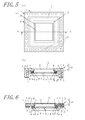
Fig. 5(a) is a top view showing another embodiment of an image pickup device according to the invention, andFig. 5(b) is a sectional view of the wiring substrate taken along the line A-A ofFig. 5(a) ; and -
Fig. 6 is a sectional view showing another embodiment of an image pickup device according to the invention. - Hereinafter, several exemplificative embodiments of the invention will be described with reference to the accompanying drawings.
- An image pickup module in accordance with a first embodiment of the invention includes, as exemplified in
Fig. 1 , animage pickup device 10, a lens securing member 11 disposed on theimage pickup device 10, and a lens 12 secured by the lens securing member 11. - The
image pickup device 10 of the first embodiment of the invention includes awiring substrate 1 and animage sensor 6. Thewiring substrate 1 includes, as exemplified inFig. 2 , an insulating substrate 1a having anopening 2 andconnection electrodes 4. Theconnection electrodes 4 are, as exemplified inFig. 3 , disposed in a surrounding region 1b around theopening 2 on the lower surface of the insulating substrate 1a, and are to be connected to theimage sensor 6. As exemplified inFig. 3 , the insulating substrate 1a has an inclined area 1c where its lower surface is inclined downward toward theopening 2. Moreover, the insulating substrate 1a has, at its lower surface, a flat area 1d which surrounds the inclined area 1c. - While the opening may be provided in the form of a penetrating
hole 2 penetrating through the insulating substrate 1a as exemplified inFig. 2 , the opening may alternatively be provided in the form of a cutout created by cutting away the insulating substrate 1a in the range from part of the side surface to the center thereof. - It is sufficient that the
connection electrodes 4 is arranged, for example, face-to-face with each other, with the penetratinghole 2 lying between them, and more preferably, is arranged so as to surround the penetratinghole 2. In the case where theconnection electrodes 4 are so arranged as to surround the penetratinghole 2, for example, given that the penetratinghole 2 is rectangular-shaped, then theconnection electrodes 4 may be arranged along three sides of the penetratinghole 2 or may be arranged along four sides of the penetratinghole 2. - According to such a
wiring substrate 1, in charging a resin acting as a bonding material 8b from a clearance at the side of the outer periphery of theimage sensor 6 toward the center thereof so that it reaches a region where thewiring substrate 1 and theimage sensor 6 confront each other, the resin is less likely to come out of a small gap at the side of the center of theinternal image sensor 6, wherefore the possibility of the spread of the resin toward a light-receiving section 6a located centrally of theimage sensor 6 can be decreased. - Moreover, as exemplified in
Figs. 1 to 3 , the insulating substrate 1a of thewiring substrate 1 may have an inclined area where its upper surface is inclined downward toward theopening 2. With such a configuration, in the case where the inclined areas of the upper surface opposed to each other with the penetratinghole 2 lying therebetween have the same inclination, in placing a light-transmittable member 9 on the inclined area 1c of the upper surface of the insulating substrate 1a so as to cover the penetratinghole 2, the light-transmittable member 9 lies flat and can therefore be placed in a predetermined position. - Moreover, the distance between the light-
transmittable member 9 and the light-receiving section 6a of theimage sensor 6 can be reduced, and this is effective in decreasing the possibility that an image seen in the light-receiving section 6a will appear blurred. - The insulating substrate 1a constituting the
wiring substrate 1 is made of an insulator such as ceramics or resin. In the case where it is made of ceramics, for example, aluminum oxide sintered body (alumina ceramics), aluminum nitride sintered body, mullite sintered body, glass ceramics sintered body, and the like can be used, whereas, in the case where it is made of resin, for example, epoxy resin, polyimide resin, acrylic resin, phenol resin, polyester resin, fluorine resin such as tetrafluoroethylene resin, and the like can be used. In addition, like glass epoxy resin, a material that is impregnated into a base material made of glass fiber can also be used. - In the case where the insulating substrate 1a is made for example of aluminum oxide sintered body, it can be produced by admixing suitable organic solvent and solution medium in powder of a raw material such as alumina (Al2O3), silica (SiO2), calcia (CaO), and magnesia (MgO) to form a slurry, shaping the slurry into a sheet-like form by a heretofore known technique such as the doctor blade method and the calender roll method to obtain a ceramic green sheet, performing appropriate punching operation on the ceramic green sheet and stacking a plurality of ceramic green sheets on top of each other on an as needed basis, and performing firing under a high-temperature condition (in the range of about 1500 to 1800°C). The penetrating
hole 2 and acavity 7 of thewiring substrate 1 can be formed by creating through holes for the penetratinghole 2 and thecavity 7 in a number of ceramic green sheets for the insulating substrate 1a by means of punching using a die or punch, laser machining, or otherwise. Moreover, as exemplified inFigs. 1 to 3 , in the case of forming thecavity 7 in thewiring substrate 1, thecavity 7 can be formed by creating a through hole for thecavity 7 in ceramic green sheets in a manner such that the through hole is larger than the through hole for the penetratinghole 2, and stacking the ceramic green sheets on top of each other in layers. - Moreover, where the inclination of the lower surface around the penetrating
hole 2 in thewiring substrate 1 is concerned, for example, in the case where thewiring substrate 1 is made of ceramics, the inclination can be obtained by, for example, placing thewiring substrate 1 in a yet-to-be-fired state on a jig which has the same shape as thewiring substrate 1 in a plan view and is inclined toward the center of the penetratinghole 2 and has a large number of holes capable of permeation of gas such as air, and whereafter sucking the lower side of the jig under a reduced pressure by means of a vacuum pump or otherwise. Alternatively, by, for example, placing thewiring substrate 1 in a yet-to-be-fired state on a jig which has the same shape as thewiring substrate 1 in a plan view and is inclined toward the center of the penetratinghole 2 and is made of metal having a high melting point, such as tungsten (W) or molybdenum (Mo), and then firing is performed on thewiring substrate 1 placed on the jig, whereby an inclination conforming to the shape of the jig can be obtained. It is also possible to impart an inclination in stepped form by repeated application of an insulating paste which is substantially the same material as that for the insulating substrate 1a. Note that, in forming a concavity portion around the penetratinghole 2 of thewiring substrate 1, where the concavity portion is made by the application of an insulating paste, it is preferable to, in addition to creating the concavity portion with use of the insulating paste, form a stepped inclination from the standpoint of productivity improvement. - The inclination obtained by such a method is preferably such that the difference in level between the highest and lowest points of the region where the
image sensor 6 is bonded to thewiring substrate 1 by the resin acting as the bonding material 8b is about 20 to 30 µm, which is substantially equal to the sum of the thickness of theconnection electrode 4 and the thickness of a connecting member 8a. For example, given that the width of the region where theimage sensor 6 is bonded to thewiring substrate 1 by the bonding material 8b is 1 mm, then the inclination is about 1.5 to 3°. - Moreover, the inclination is preferably disposed between the
connection electrode 4 formed around the through hole and the through hole, or is disposed in a region around the through hole that is free of theconnection electrode 4. In such a case, since theconnection electrode 4 is not inclined, it follows that awiring conductor 3 and theimage sensor 6 can be electrically connected to each other without fail, and also the distance between thewiring substrate 1 and theimage sensor 6 in the connection electrode 4-free region is larger than that in the connection electrode 4-bearing region, wherefore the resin is restrained from spreading therefrom toward the light-receiving section 6a. - In the case where the insulating substrate 1a of the
wiring substrate 1 is made for example of resin, it can be formed by means of transfer molding, injection molding, or otherwise with use of a mold capable of providing a predetermined shape of thewiring substrate 1. Moreover, a material that is impregnated into a base material made of glass fiber may also be used. In this case, the insulating substrate can be formed by impregnating a precursor epoxy resin into a base material made of glass fiber and thermally curing the precursor epoxy resin at a predetermined temperature. - When the insulating substrate 1a is made of ceramics, the
wiring conductor 3, theconnection electrode 4 and theexternal terminal 5 are made of metalized powder of tungsten (W), molybdenum (Mo), manganese (Mn), silver (Ag), copper (Cu), or the like and is formed at a predetermined position of thewiring substrate 1 by printing a metalized paste for thewiring conductor 3 on a ceramic green sheet for the insulating substrate 1a in a predetermined shape by screen printing or the like and co-firing the metalized paste together with the ceramic green sheet for the insulating substrate 1a. Out of internal conductors, a penetrating conductor penetrating through the ceramic green sheets in a thickness direction thereof may advisably be formed by filling a through hole disposed in the ceramic green sheets with a conductor paste by means of printing. Such a conductor paste is prepared by kneading the above-described metal powder in admixture with suitable solvent and binder while adjusting the viscosity to an appropriate level. Note that, in the interest of enhancement in the strength of the bonding with thewiring substrate 1, the conductor paste may contain glass or ceramics. - When the insulating substrate 1a is made of resin, the
wiring conductor 3, theconnection electrode 4 and theexternal terminal 5 are made of metal materials such as copper, gold, aluminum, nickel, chromium, molybdenum, titanium, and alloys thereof. For example, a copper foil processed in the shape of theconductor 3 is transferred onto a resin sheet made of a glass epoxy resin, the resin sheets onto which the copper foil is transferred are stacked and attached by an adhesive. Out of the internal conductors, the penetrating conductor that penetrates in the thickness direction of the resin sheet may be formed by depositing a conductor paste on the inner surface of the through hole that is formed in the resin sheet according to printing or plating or may be formed by filling the through hole. Further, the penetrating conductor is formed by integrating a metal foil and a metal pillar by resin molding or depositing the metal foil on the insulating substrate 1a using sputtering, evaporation, plating, or the like. - The exposed surfaces of the
wiring conductor 3, theconnection electrode 4, and theexternal terminal 5 are coated with a plating layer by a plating technique such as electrolytic plating or electroless plating. The plating layer is made of a metal which excels in corrosion resistance and in connectivity with a connection terminal 6b, such as nickel and gold. For example, a nickel plating layer having a thickness of approximately 1 to 10 µm and a gold plating layer having a thickness of approximately 0.1 to 3 µm are deposited one after another. This makes it possible to suppress thewiring conductor 3, theconnection electrode 4, and theexternal terminal 5 from corrosion effectively, as well as to strengthen the bonding between the connection terminal 6b of theimage sensor 6 and theconnection electrode 4 and the connection between theexternal terminal 5 and a wiring conductor of an external circuit board. - The mounting of the
image sensor 6 on thewiring substrate 1 is, as exemplified inFig. 1 , accomplished by establishing electrical and mechanical connection between an electrode of theimage sensor 6 and theconnection terminal 6 placed on thewiring substrate 1 via the connecting member 8a such as a solder bump, a gold bump, or an electrically conducting resin (such as an anisotropic conductive resin). Moreover, in this case, after the connection is established via the bump acting as the connecting member 8a, as a so-called underfill, the bonding material 8b made of resin is poured in between theimage sensor 6 and thewiring substrate 1. Note that, in the case of using an anisotropic conductive resin as the connecting member 8a, the electrical connection and the bonding between thewiring substrate 1 and theimage sensor 6 can be accomplished at the same time. - As the connecting member 8a, a resin material such as epoxy resin and a composite resin composed predominantly of epoxy resin can be used.
- Next, the
image sensor 6 of CCD type or CMOS type is placed under thewiring substrate 1 so that the light-receiving section 6a can be located inside the penetratinghole 2, and, the electrode of theimage sensor 6 and theconnection terminal 6 placed on thewiring substrate 1 are electrically and mechanically connected to each other for flip-chip connection via the connecting member 8a such as a solder bump, a gold bump, or an electrically conducting resin (such as an anisotropic conductive resin) so that the connection terminal 6b and theconnection electrode 4 can be electrically connected to each other. In such a case, the flip-chip connection can be achieved by means of solder bonding, gold-bump ultrasonic bonding, or anisotropic conductive resin bonding. Note that, in the case of effecting the flip-chip connection using a solder bump or a gold bump, the bonding material 8b is charged for the sake of strengthening the bonding between the connection terminal 6b of theimage sensor 6 and theconnection electrode 4, and sealing the penetratinghole 2 for the protection of the light-receiving section 6a. - Moreover, as exemplified in
Fig. 1 , in theimage pickup device 10 such as shown hereinabove, a light-transmittable member 9 is attached to the upper surface of thewiring substrate 1 so as to close the penetratinghole 2. In such a structure, it never occurs that moisture or dust finds its way into the penetratinghole 2 and eventually adheres to the light-receiving section 6a of theimage sensor 6, wherefore it is possible to provide protection for theimage sensor 6, as well as to produce output of high-quality image signals without hindrance to the receiving of light. For example, it is possible to prevent the waste produced when the lens securing member 11 with the lens 12 secured thereto is bonded to the upper surface of thewiring substrate 1 from finding its way into the penetratinghole 2 and from eventually adhering to the light-receiving section 6a of theimage sensor 6. - Further, in mounting the
image sensor 6 on thewiring substrate 1, it is preferable that, after supporting thewiring substrate 1 so that theconnection electrode 4 thereof faces upward, theimage sensor 6 is installed thereon from above, and then a resin acting as the bonding material 8b is charged into the region where thewiring substrate 1 and theimage sensor 6 confront each other. In such a case, by virtue of the inclination provided at the lower surface (upward-facing surface in this construction) of thewiring substrate 1, the resin flows downward by gravitation and can therefore be restrained from spreading onto the light-receiving section 6a more reliably. In the case where the concavity portion is disposed around the penetratinghole 2 of thewiring substrate 1, likewise, the resin tends to be accumulated inside the concavity portion by gravitation and can therefore be restrained from spreading onto the light-receiving section 6a even more reliably. - The light-
transmittable member 9, which is made of quartz, glass, resin such as epoxy resin, or the like, is bonded to thewiring substrate 1 by an adhesive such as thermosetting epoxy resin, ultraviolet-curable epoxy resin or glass. For example, an adhesive made of ultraviolet-curable epoxy resin is applied to the upper surface of thewiring substrate 1 around the through hole or to the outer edge of the light-transmittable member 9 by a dispensing technique, and then the light-transmittable member 9 is placed on thewiring substrate 1 with subsequent ultraviolet irradiation, whereby the adhesive can be cured for sealing of the construction. A filter may be formed on the light-transmittable member 9. In this case, as compared with the case of placing a separately prepared filter on the light-transmittable member 9, the thickness of theimage pickup device 10 can be reduced. Accordingly, it is preferable to do so. - As the filter, there is a low-pass filter constructed of a stack of two or three crystal plates of different angles of crystal orientation, which is capable of preventing a moire phenomenon from occurring in an image taken by the
image sensor 6 by exploiting the birefringent characteristics of the crystal plates. In the case of using a crystal plate as the light-transmittable member 9, the light-transmittable member 9 is able to serve also as one of the crystal plates of the low-pass filter. - Also, there is an IR cutoff filter for cutting off light in a red to infrared wavelength region, which serves the purpose of adapting the
image sensor 6, which generally exhibits higher sensitivity to light in a red to infrared region than do human eyes, to the color-tone sensitivity of human eyes. The IR cutoff filter can be fabricated by forming several dozens of dielectric multilayer films in alternate order on the surface of the light-transmittable member 9. The dielectric multilayer film is customarily formed by stacking several dozens of high-refractive-index dielectric layers made of a dielectric material having a refractive index of greater than or equal to 1.7 and low-refractive-index dielectric layers made of a dielectric material having a refractive index of less than or equal to 1.6 in alternate order by means of vapor deposition, sputtering, or otherwise. Examples of the dielectric material having a refractive index of greater than or equal to 1.7 include tantalum pentoxide, titanium oxide, niobium pentoxide, lanthanum oxide, and zirconium oxide. Examples of the dielectric material having a refractive index of less than or equal to 1.6 include silicon oxide, aluminum oxide, lanthanum fluoride, and magnesium fluoride. - The lens 12, which is made of glass, resin such as epoxy resin, or the like, is attached to the lens securing member 11, and the light which has been transmitted through the lens 12 via the opening of the lens securing member 11 is allowed to enter the light-receiving section 6a. The lens securing member 11 is made of resin, metal, or the like, and is, as exemplified in
Fig. 1 , fixed to the upper surface of thewiring substrate 1 by an adhesive such as epoxy resin or solder, or fixed to thewiring substrate 1 by a hook or the like formed in advance in the lens securing member 11. - The
image pickup device 10 in accordance with a second embodiment of the invention differs from the first embodiment in that: as exemplified inFig. 4 , the surrounding region 1b of the lower surface of the insulating substrate 1a includes an inclined area 1c surrounding the penetratinghole 2 and a flat area 1d surrounding the inclined area 1c, and a plurality ofconnection electrodes 4 are arranged on the flat area 1d. Otherwise, the second embodiment is similar in structure to the first embodiment. - In such an
image pickup device 10 of the second embodiment, the light-receiving section 6a of theimage sensor 6 can be located at the side of the upper surface of thewiring substrate 1, wherefore the distance between the light-transmittable member 9 disposed on the upper surface of thewiring substrate 1 so as to cover the penetratinghole 2 and the light-receiving section 6a can be reduced, which is effective in decreasing the possibility that an image seen in the light-receiving section 6a will appear blurred. - The
image pickup device 10 in accordance with a third embodiment of the invention differs from the first embodiment in that: as exemplified inFig. 5 , the insulating substrate 1a has a concavity portion located in, of its lower surface, an edge portion surrounding the penetratinghole 2. Otherwise, the third embodiment is similar in structure to the first embodiment. - In such an
image pickup device 10 of the third embodiment, when a resin acting as a bonding material 8b is charged from a clearance at the side of the outer periphery of theimage sensor 6 toward the center thereof so as to reach a region where thewiring substrate 1 and theimage sensor 6 confront each other, even if the resin finds its way toward the center of theimage sensor 6 beyond the region where thewiring substrate 1 and theimage sensor 6 confront each other, the resin is accumulated in the concavity portion, which is effective in decreasing the possibility of the spread of the resin toward the light-receiving section 6a. - Moreover, as exemplified in
Fig. 5 , in the case of forming the concavity portion along the opening at the lower side of the penetratinghole 2 of thewiring substrate 1, the formation can be achieved by creating a first through hole for the penetratinghole 2 in a ceramic green sheet, then creating a second through hole in a different ceramic green sheet from the ceramic green sheet formed with the first through hole so that the second through hole is larger than the first through hole, and stacking these ceramic green sheets on top of each other in layers. Note that each ceramic green sheet may be of a stack of a plurality of ceramic green sheets. In this case, by forming a through hole after the stacking together of a plurality of ceramic green sheets, it is possible to obtain a highly accurate through hole without any influence of sheet misalignment in stacking process. Note that, as exemplified inFig. 5 , in the case where both the concavity portion and thecavity 7 are formed in thewiring substrate 1, it is advisable to form the second through hole so that it is smaller than the through hole for thecavity 7. Moreover, the concavity portion can also be formed by the application of an insulating paste made of a material which is substantially the same as that for ceramic green sheets. In the case of forming the concavity portion with use of the insulating paste, the concavity portion is preferably configured to have a depth of approximately 20 to 30 µm, whereas, in the case of forming the concavity portion with use of ceramic green sheets, the concavity portion is preferably configured to have a depth of approximately 50 µm to 1 mm. - Moreover, as exemplified in
Fig. 5 , in the case where the concavity portion is formed at a midpoint of the inclination around the penetratinghole 2 of thewiring substrate 1, it is preferable that the concavity portion has its bottom located toward the top side beyond the flat area 1d. This makes it possible to prevent the edge portion of the lower surface of thewiring substrate 1 from colliding against theimage sensor 6 when mounting theimage sensor 6 on thewiring substrate 1, with the consequent occurrence of breakage of theimage sensor 6. Moreover, by imparting an inclination to the concavity portion, it is possible to prevent the spread of the resin onto the light-receiving section 6a of theimage sensor 6 more reliably. Accordingly it is preferable to do so. - The
image pickup device 10 in accordance with a fourth embodiment of the invention differs from the first embodiment in that: as exemplified inFig. 6 , the insulating substrate 1a has an upper surface including a recess portion 14 for placing an electronic component 13, the recess portion 14 is located around the inclined area 1c in a plan view, and thewiring substrate 1 is shaped like a flat plate. Otherwise, the fourth embodiment is similar in structure to the first embodiment. - Such an
image pickup device 10 of the fourth embodiment is effective in decreasing blocking of light which is incident on the light-receiving section 6a caused by adhesion of a bonding material 8b for bonding the electronic component 13 to thewiring substrate 1 to the interior of the penetratinghole 2 or the light-transmittable member 9. - Moreover, since the recess portion 14 is placed in the flat area 1d around the inclined area 1c, it is possible to eliminate the condition that the thickness of the inclined area 1c should be reduced, which is effective in imparting a predetermined inclination to the inclined area 1c.
- In forming such a recess portion 14, it is advisable to create a thin film made of an appropriate insulator after forming a connection terminal of the wiring substrate for connection with the electronic component. In the case where the
wiring substrate 1 is made of ceramics, the formation can be achieved by applying a ceramic paste which is composed of substantially the same material as the insulating substrate 1a prior to firing process or by applying an organic resin or the like after firing process. - Moreover, since the
wiring substrate 1 is configured to have a flat-plate shape, it follows that, when a plurality of green sheets that constitute thewiring substrate 1 are stacked and pressure-bonded together in the course of production of thewiring substrate 1 by a green-sheet lamination method, the sheets as a whole are subjected to pressure of uniform level, wherefore it is possible to suppress accidental distortion of thewiring substrate 1. Further, in the case where thewiring substrate 1 is made of ceramics, in some cases, a load is applied to thewiring substrate 1 for the prevention of occurrence of warpage in thewiring substrate 1 during firing process, and, in this regard, since the outer periphery of thewiring substrate 1 has a flat-plate form, it is easy to apply a load to a predetermined region of the outer periphery of thewiring substrate 1. - The electronic component 13 such as an IC for electric signal processing, a capacitor, a coil or a resistor, is installed through the connection with the
wiring conductor 3 by an electrically conducting bonding material 8b such as solder, for example. The electronic component 13 can either be mounted on thewiring substrate 1 after the bonding of thewiring substrate 1 with theimage sensor 6, or be mounted on thewiring substrate 1 prior to that bonding operation. - It is noted that, in the
wiring substrate 1 having thecavity 7 as exemplified inFigs. 1 to 5 , in the case where the electronic component 13 is installed so as to be positioned in overlapping relation to thecavity 7 in a plan view, it is preferable to mount theimage sensor 6 on thewiring substrate 1 after the mounting of the electronic component 13 on thewiring substrate 1. This makes it possible to suppress separation of the connection terminal 6b of theimage sensor 6 from theconnection electrode 4 due to the impact at the time of mounting the electronic component 13. - In the case of mounting the electronic component 13 on the
wiring substrate 1, when the electronic component 13 is mounted in theimage pickup device 10 including thewiring substrate 1 having thecavity 7 as exemplified inFigs. 1 to 5 , in order to suppress occurrence of problem such as breakage, it is preferable to place thewiring substrate 1 on a support plate jig having a projection which conforms to the shape of the penetratinghole 2 of thewiring substrate 1. - Moreover, in the case of mounting the electronic component 13 with solder after the bonding of the
wiring substrate 1 with theimage sensor 6, it is preferable to mount the electronic component 13 following the completion of attachment of the light-transmittable member 9. This makes it possible to prevent a flux and solder particles contained in a solder cream from scattering around and eventually adhering to the light-receiving section 6a of theimage sensor 6. - It should be understood that the application of the invention is not limited to the specific embodiments described heretofore, and that many modifications and variations of the invention are possible without departing from the scope of the invention.
- For example, the
image pickup device 10 may be so designed that sidewall portions are formed in vertically or horizontally opposed positions in a plan view, and theimage sensor 6 is housed in a vertically or horizontally openedcavity 7 in a plan view. In this case, in bonding thewiring substrate 1 to a wiring substrate, it is possible to achieve the bonding operation while emitting heat and gas generated inside thecavity 7 to the outside, which is effective in preventing deformation of thewiring substrate 1 when it is bonded to the wiring substrate. - Moreover, the inclined area of the lower surface of the
wiring substrate 1 around theopening 2 may be either formed around the entire perimeter of the penetratinghole 2 or formed along part of the perimeter. In the case where the region in which theimage sensor 6 is bonded to thewiring substrate 1 by the resin acting as the bonding material 8b varies in width from part to part around the perimeter of the penetratinghole 2, the inclination may be formed only in a small-width part of that region at which the bonding material tends to spread toward the light-receiving section 6a. Further, the angle of inclination may be varied in the bonded region in accordance with the width of the bonded region and the position of theconnection electrode 4. -
- 1: Wiring substrate
- 1a: Insulating substrate
- 1b: Surrounding region
- 1c: Inclined area
- 1d: Flat area
- 2: Penetrating hole
- 3: Wiring conductor
- 4: Connection electrode
- 5: External terminal
- 6: Image sensor
- 6a: Light-receiving section
- 6b: Connection terminal
- 7: Cavity
- 8a: Connecting member
- 8b: Bonding material
- 9: Light-transmittable member
- 10: Image pickup device
- 11: Lens securing member
- 12: Lens
- 13: Electronic component
- 14: Recess portion
Claims (8)
- A wiring substrate, comprising:an insulating substrate having an opening; anda plurality of connection electrodes disposed in a surrounding region around the opening on a lower surface of the insulating substrate, the plurality of connection electrodes being to be electrically connected to an image sensor,the surrounding region having an inclined area, the inclined area surrounding the opening and being inclined downward toward the opening.
- The wiring substrate according to claim 1, wherein the lower surface of the insulating substrate has a concavity portion located in a part at an edge of the opening.
- The wiring substrate according to claim 1, wherein the surrounding region has a flat area which surrounds the inclined area, and
the plurality of connection electrodes are disposed in the flat area. - The wiring substrate according to claim 1, wherein the insulating substrate has an upper surface having a recess portion for placement of an electronic component.
- The wiring substrate according to claim 4, wherein the recess portion is located around the inclined area in a plan view.
- The wiring substrate according to claim 1, wherein an upper surface of the insulating substrate has an inclined area which is inclined downward toward the opening.
- An image pickup device, comprising:the wiring substrate according to any one of claims 1 to 6; andan image sensor mounted on the lower surface of the insulating substrate of the wiring substrate and electrically connected to the plurality of connection electrodes.
- An image pickup module, comprising:the image pickup device according to claim 7; anda lens disposed above the opening.
Applications Claiming Priority (2)
| Application Number | Priority Date | Filing Date | Title |
|---|---|---|---|
| JP2010146463 | 2010-06-28 | ||
| PCT/JP2011/064794 WO2012002378A1 (en) | 2010-06-28 | 2011-06-28 | Wiring substrate, image pickup device, and image-pickup device module |
Publications (3)
| Publication Number | Publication Date |
|---|---|
| EP2587793A1 true EP2587793A1 (en) | 2013-05-01 |
| EP2587793A4 EP2587793A4 (en) | 2014-04-16 |
| EP2587793B1 EP2587793B1 (en) | 2020-01-08 |
Family
ID=45402085
Family Applications (1)
| Application Number | Title | Priority Date | Filing Date |
|---|---|---|---|
| EP11800842.4A Active EP2587793B1 (en) | 2010-06-28 | 2011-06-28 | Image pickup device and image-pickup device module |
Country Status (6)
| Country | Link |
|---|---|
| US (1) | US20130128109A1 (en) |
| EP (1) | EP2587793B1 (en) |
| JP (1) | JP5491628B2 (en) |
| KR (1) | KR20130120981A (en) |
| CN (1) | CN102893593B (en) |
| WO (1) | WO2012002378A1 (en) |
Cited By (1)
| Publication number | Priority date | Publication date | Assignee | Title |
|---|---|---|---|---|
| EP3664140A1 (en) * | 2018-12-05 | 2020-06-10 | Azurewave Technologies, Inc. | Image capturing module and portable electronic device |
Families Citing this family (18)
| Publication number | Priority date | Publication date | Assignee | Title |
|---|---|---|---|---|
| WO2013180288A1 (en) * | 2012-05-31 | 2013-12-05 | 京セラ株式会社 | Substrate for mounting electronic element, and electronic device |
| JP6022888B2 (en) * | 2012-10-19 | 2016-11-09 | 京セラ株式会社 | Electronic device mounting substrate and electronic device |
| JP6150249B2 (en) * | 2013-02-25 | 2017-06-21 | 京セラ株式会社 | Glass sealing method for electronic device |
| US9608020B2 (en) * | 2013-10-23 | 2017-03-28 | Kyocera Corporation | Imaging element mounting substrate and imaging device |
| CN204651317U (en) * | 2014-06-10 | 2015-09-16 | 意法半导体(格勒诺布尔2)公司 | Comprise the electronic equipment of optical sensor chip |
| KR20160080166A (en) * | 2014-12-29 | 2016-07-07 | 에스케이하이닉스 주식회사 | Embedded image sensor package and method of fabricating the same |
| CN105530413B (en) * | 2015-12-01 | 2019-08-30 | 宁波舜宇光电信息有限公司 | Camera module and its electrical support and line conduction method |
| CN105472215A (en) * | 2015-12-01 | 2016-04-06 | 宁波舜宇光电信息有限公司 | Camera module group with electrical support, and assembly method and application of camera module group |
| KR102248434B1 (en) | 2015-12-01 | 2021-05-04 | 닝보 써니 오포테크 코., 엘티디. | Image capturing module and electrical support thereof |
| CN108450036B (en) * | 2015-12-24 | 2023-03-28 | 京瓷株式会社 | Substrate for mounting imaging element and imaging device |
| JP2017139258A (en) * | 2016-02-01 | 2017-08-10 | ソニー株式会社 | Image pickup device package and image pickup apparatus |
| JP6949515B2 (en) * | 2017-03-15 | 2021-10-13 | ソニーセミコンダクタソリューションズ株式会社 | Camera modules, their manufacturing methods, and electronic devices |
| CN111466028A (en) * | 2017-10-26 | 2020-07-28 | 京瓷株式会社 | Imaging element mounting substrate, imaging device, and imaging module |
| US11515242B2 (en) * | 2017-12-28 | 2022-11-29 | Kyocera Corporation | Wiring substrate, electronic device, and electronic module each having plate-shaped conductive portion in frame portion of insulation substrate |
| JP6976201B2 (en) * | 2018-03-13 | 2021-12-08 | 京セラ株式会社 | Manufacturing Methods for Fixed Structures, Electronic Devices, Imaging Devices, Mobiles, and Fixed Structures |
| CN111866322A (en) * | 2019-04-30 | 2020-10-30 | 宁波舜宇光电信息有限公司 | Camera module and its photosensitive assembly, electronic equipment and preparation method |
| TWI762093B (en) | 2020-12-18 | 2022-04-21 | 海華科技股份有限公司 | Portable electronic device and customized image capturing module thereof |
| CN216162757U (en) * | 2021-05-25 | 2022-04-01 | 三赢科技(深圳)有限公司 | Lens module and electronic device |
Family Cites Families (30)
| Publication number | Priority date | Publication date | Assignee | Title |
|---|---|---|---|---|
| JPS58140156A (en) * | 1982-02-16 | 1983-08-19 | Canon Inc | Solid-state image pickup device |
| JP4004705B2 (en) * | 2000-02-29 | 2007-11-07 | 松下電器産業株式会社 | Imaging device and imaging device assembling method |
| JP2001358997A (en) * | 2000-06-12 | 2001-12-26 | Mitsubishi Electric Corp | Semiconductor device |
| JP2002134763A (en) * | 2000-10-27 | 2002-05-10 | Kyocera Corp | Semiconductor light receiving element storage container |
| JP2002305261A (en) * | 2001-01-10 | 2002-10-18 | Canon Inc | Electronic component and method of manufacturing the same |
| US20050051859A1 (en) * | 2001-10-25 | 2005-03-10 | Amkor Technology, Inc. | Look down image sensor package |
| JP5030360B2 (en) * | 2002-12-25 | 2012-09-19 | オリンパス株式会社 | Method for manufacturing solid-state imaging device |
| JP3768972B2 (en) * | 2003-04-28 | 2006-04-19 | 松下電器産業株式会社 | Solid-state imaging device and manufacturing method thereof |
| JP2004341201A (en) * | 2003-05-15 | 2004-12-02 | Konica Minolta Opto Inc | Imaging unit |
| JP4303610B2 (en) * | 2003-05-19 | 2009-07-29 | 富士フイルム株式会社 | Multilayer wiring board, component mounting method, and imaging apparatus |
| JP4411893B2 (en) * | 2003-07-28 | 2010-02-10 | パナソニック電工株式会社 | Solid circuit board and imaging device |
| JP4012924B2 (en) * | 2003-09-30 | 2007-11-28 | 富士通株式会社 | The camera module |
| JP4170968B2 (en) * | 2004-02-02 | 2008-10-22 | 松下電器産業株式会社 | Optical device |
| KR100609012B1 (en) * | 2004-02-11 | 2006-08-03 | 삼성전자주식회사 | Wiring board and semiconductor device for solid-state imaging using same |
| US20060016973A1 (en) * | 2004-07-21 | 2006-01-26 | Advanced Semiconductor Engineering, Inc. | Multi-chip image sensor package module |
| WO2006011200A1 (en) * | 2004-07-28 | 2006-02-02 | Fujitsu Limited | Imaging apparatus |
| JP4428526B2 (en) * | 2004-10-15 | 2010-03-10 | パナソニック株式会社 | Optical device |
| JP4196937B2 (en) * | 2004-11-22 | 2008-12-17 | パナソニック株式会社 | Optical device |
| JP2006201427A (en) * | 2005-01-20 | 2006-08-03 | Kyocera Corp | Imaging element storage package, imaging apparatus, and imaging module |
| JP2007027452A (en) * | 2005-07-19 | 2007-02-01 | Matsushita Electric Ind Co Ltd | Solid-state image sensor module and method for manufacturing solid-state image sensor module |
| TWI308456B (en) * | 2005-12-30 | 2009-04-01 | Advanced Semiconductor Eng | Compact camera module and method for fabricating the same |
| JP2007299929A (en) * | 2006-04-28 | 2007-11-15 | Matsushita Electric Ind Co Ltd | Optical device apparatus and optical device module using the same |
| KR100790994B1 (en) * | 2006-08-01 | 2008-01-03 | 삼성전자주식회사 | Image sensor module comprising an image sensor package, a method of manufacturing the same, and an image sensor package |
| US20080136012A1 (en) * | 2006-12-08 | 2008-06-12 | Advanced Chip Engineering Technology Inc. | Imagine sensor package and forming method of the same |
| JP2008263550A (en) * | 2007-04-13 | 2008-10-30 | Matsushita Electric Ind Co Ltd | Solid-state imaging device and manufacturing method thereof |
| JP2008263552A (en) * | 2007-04-13 | 2008-10-30 | Matsushita Electric Ind Co Ltd | Solid-state imaging device and manufacturing method thereof |
| US20090179290A1 (en) * | 2008-01-15 | 2009-07-16 | Huang Shuangwu | Encapsulated imager packaging |
| JP2010238995A (en) * | 2009-03-31 | 2010-10-21 | Sanyo Electric Co Ltd | Semiconductor module and camera module equipped with the same |
| JP2011101228A (en) * | 2009-11-06 | 2011-05-19 | Toshiba Corp | Ceramic package and camera module |
| EP2506302B1 (en) * | 2009-11-26 | 2021-08-11 | Kyocera Corporation | Wiring substrate, imaging device and imaging device module |
-
2011
- 2011-06-28 KR KR1020127031487A patent/KR20130120981A/en not_active Ceased
- 2011-06-28 JP JP2012522638A patent/JP5491628B2/en active Active
- 2011-06-28 US US13/701,443 patent/US20130128109A1/en not_active Abandoned
- 2011-06-28 CN CN201180024080.9A patent/CN102893593B/en active Active
- 2011-06-28 EP EP11800842.4A patent/EP2587793B1/en active Active
- 2011-06-28 WO PCT/JP2011/064794 patent/WO2012002378A1/en not_active Ceased
Cited By (1)
| Publication number | Priority date | Publication date | Assignee | Title |
|---|---|---|---|---|
| EP3664140A1 (en) * | 2018-12-05 | 2020-06-10 | Azurewave Technologies, Inc. | Image capturing module and portable electronic device |
Also Published As
| Publication number | Publication date |
|---|---|
| EP2587793A4 (en) | 2014-04-16 |
| EP2587793B1 (en) | 2020-01-08 |
| KR20130120981A (en) | 2013-11-05 |
| CN102893593A (en) | 2013-01-23 |
| US20130128109A1 (en) | 2013-05-23 |
| WO2012002378A1 (en) | 2012-01-05 |
| CN102893593B (en) | 2016-11-23 |
| JPWO2012002378A1 (en) | 2013-08-29 |
| JP5491628B2 (en) | 2014-05-14 |
Similar Documents
| Publication | Publication Date | Title |
|---|---|---|
| EP2587793B1 (en) | Image pickup device and image-pickup device module | |
| US8659105B2 (en) | Wiring substrate, imaging device and imaging device module | |
| US8866067B2 (en) | Imaging device with an imaging element and an electronic component | |
| US11075235B2 (en) | Image sensor mounting base, imaging device, and imaging module | |
| CN103959466B (en) | Imaging apparatuss storage is encapsulated and camera head | |
| CN104885213B (en) | Photographing element mounting substrate and camera device | |
| US9608020B2 (en) | Imaging element mounting substrate and imaging device | |
| JP5595066B2 (en) | Imaging device and imaging module | |
| CN105144686B (en) | Photographing element board for mounting electronic and photographic device | |
| US9826641B2 (en) | Electronic device mounting board and electronic apparatus | |
| JP5460356B2 (en) | Imaging device |
Legal Events
| Date | Code | Title | Description |
|---|---|---|---|
| PUAI | Public reference made under article 153(3) epc to a published international application that has entered the european phase |
Free format text: ORIGINAL CODE: 0009012 |
|
| 17P | Request for examination filed |
Effective date: 20130128 |
|
| AK | Designated contracting states |
Kind code of ref document: A1 Designated state(s): AL AT BE BG CH CY CZ DE DK EE ES FI FR GB GR HR HU IE IS IT LI LT LU LV MC MK MT NL NO PL PT RO RS SE SI SK SM TR |
|
| DAX | Request for extension of the european patent (deleted) | ||
| A4 | Supplementary search report drawn up and despatched |
Effective date: 20140319 |
|
| RIC1 | Information provided on ipc code assigned before grant |
Ipc: H05K 1/02 20060101ALI20140313BHEP Ipc: H04N 5/335 20110101AFI20140313BHEP Ipc: H01L 27/146 20060101ALI20140313BHEP Ipc: H04N 5/225 20060101ALI20140313BHEP |
|
| RIN1 | Information on inventor provided before grant (corrected) |
Inventor name: ICHIKI,SHINJI Inventor name: SEGAWA,HIROYUKI |
|
| 17Q | First examination report despatched |
Effective date: 20150730 |
|
| STAA | Information on the status of an ep patent application or granted ep patent |
Free format text: STATUS: EXAMINATION IS IN PROGRESS |
|
| GRAP | Despatch of communication of intention to grant a patent |
Free format text: ORIGINAL CODE: EPIDOSNIGR1 |
|
| STAA | Information on the status of an ep patent application or granted ep patent |
Free format text: STATUS: GRANT OF PATENT IS INTENDED |
|
| INTG | Intention to grant announced |
Effective date: 20190806 |
|
| RIN1 | Information on inventor provided before grant (corrected) |
Inventor name: SEGAWA, HIROYUKI Inventor name: ICHIKI, SHINJI |
|
| GRAS | Grant fee paid |
Free format text: ORIGINAL CODE: EPIDOSNIGR3 |
|
| GRAA | (expected) grant |
Free format text: ORIGINAL CODE: 0009210 |
|
| STAA | Information on the status of an ep patent application or granted ep patent |
Free format text: STATUS: THE PATENT HAS BEEN GRANTED |
|
| AK | Designated contracting states |
Kind code of ref document: B1 Designated state(s): AL AT BE BG CH CY CZ DE DK EE ES FI FR GB GR HR HU IE IS IT LI LT LU LV MC MK MT NL NO PL PT RO RS SE SI SK SM TR |
|
| REG | Reference to a national code |
Ref country code: GB Ref legal event code: FG4D |
|
| REG | Reference to a national code |
Ref country code: CH Ref legal event code: EP |
|
| REG | Reference to a national code |
Ref country code: DE Ref legal event code: R096 Ref document number: 602011064528 Country of ref document: DE |
|
| REG | Reference to a national code |
Ref country code: IE Ref legal event code: FG4D |
|
| REG | Reference to a national code |
Ref country code: AT Ref legal event code: REF Ref document number: 1224152 Country of ref document: AT Kind code of ref document: T Effective date: 20200215 |
|
| REG | Reference to a national code |
Ref country code: NL Ref legal event code: MP Effective date: 20200108 |
|
| REG | Reference to a national code |
Ref country code: LT Ref legal event code: MG4D |
|
| PG25 | Lapsed in a contracting state [announced via postgrant information from national office to epo] |
Ref country code: FI Free format text: LAPSE BECAUSE OF FAILURE TO SUBMIT A TRANSLATION OF THE DESCRIPTION OR TO PAY THE FEE WITHIN THE PRESCRIBED TIME-LIMIT Effective date: 20200108 Ref country code: NO Free format text: LAPSE BECAUSE OF FAILURE TO SUBMIT A TRANSLATION OF THE DESCRIPTION OR TO PAY THE FEE WITHIN THE PRESCRIBED TIME-LIMIT Effective date: 20200408 Ref country code: NL Free format text: LAPSE BECAUSE OF FAILURE TO SUBMIT A TRANSLATION OF THE DESCRIPTION OR TO PAY THE FEE WITHIN THE PRESCRIBED TIME-LIMIT Effective date: 20200108 Ref country code: PT Free format text: LAPSE BECAUSE OF FAILURE TO SUBMIT A TRANSLATION OF THE DESCRIPTION OR TO PAY THE FEE WITHIN THE PRESCRIBED TIME-LIMIT Effective date: 20200531 Ref country code: RS Free format text: LAPSE BECAUSE OF FAILURE TO SUBMIT A TRANSLATION OF THE DESCRIPTION OR TO PAY THE FEE WITHIN THE PRESCRIBED TIME-LIMIT Effective date: 20200108 Ref country code: LT Free format text: LAPSE BECAUSE OF FAILURE TO SUBMIT A TRANSLATION OF THE DESCRIPTION OR TO PAY THE FEE WITHIN THE PRESCRIBED TIME-LIMIT Effective date: 20200108 |
|
| PG25 | Lapsed in a contracting state [announced via postgrant information from national office to epo] |
Ref country code: GR Free format text: LAPSE BECAUSE OF FAILURE TO SUBMIT A TRANSLATION OF THE DESCRIPTION OR TO PAY THE FEE WITHIN THE PRESCRIBED TIME-LIMIT Effective date: 20200409 Ref country code: BG Free format text: LAPSE BECAUSE OF FAILURE TO SUBMIT A TRANSLATION OF THE DESCRIPTION OR TO PAY THE FEE WITHIN THE PRESCRIBED TIME-LIMIT Effective date: 20200408 Ref country code: HR Free format text: LAPSE BECAUSE OF FAILURE TO SUBMIT A TRANSLATION OF THE DESCRIPTION OR TO PAY THE FEE WITHIN THE PRESCRIBED TIME-LIMIT Effective date: 20200108 Ref country code: LV Free format text: LAPSE BECAUSE OF FAILURE TO SUBMIT A TRANSLATION OF THE DESCRIPTION OR TO PAY THE FEE WITHIN THE PRESCRIBED TIME-LIMIT Effective date: 20200108 Ref country code: SE Free format text: LAPSE BECAUSE OF FAILURE TO SUBMIT A TRANSLATION OF THE DESCRIPTION OR TO PAY THE FEE WITHIN THE PRESCRIBED TIME-LIMIT Effective date: 20200108 Ref country code: IS Free format text: LAPSE BECAUSE OF FAILURE TO SUBMIT A TRANSLATION OF THE DESCRIPTION OR TO PAY THE FEE WITHIN THE PRESCRIBED TIME-LIMIT Effective date: 20200508 |
|
| REG | Reference to a national code |
Ref country code: DE Ref legal event code: R097 Ref document number: 602011064528 Country of ref document: DE |
|
| PG25 | Lapsed in a contracting state [announced via postgrant information from national office to epo] |
Ref country code: ES Free format text: LAPSE BECAUSE OF FAILURE TO SUBMIT A TRANSLATION OF THE DESCRIPTION OR TO PAY THE FEE WITHIN THE PRESCRIBED TIME-LIMIT Effective date: 20200108 Ref country code: CZ Free format text: LAPSE BECAUSE OF FAILURE TO SUBMIT A TRANSLATION OF THE DESCRIPTION OR TO PAY THE FEE WITHIN THE PRESCRIBED TIME-LIMIT Effective date: 20200108 Ref country code: SM Free format text: LAPSE BECAUSE OF FAILURE TO SUBMIT A TRANSLATION OF THE DESCRIPTION OR TO PAY THE FEE WITHIN THE PRESCRIBED TIME-LIMIT Effective date: 20200108 Ref country code: RO Free format text: LAPSE BECAUSE OF FAILURE TO SUBMIT A TRANSLATION OF THE DESCRIPTION OR TO PAY THE FEE WITHIN THE PRESCRIBED TIME-LIMIT Effective date: 20200108 Ref country code: SK Free format text: LAPSE BECAUSE OF FAILURE TO SUBMIT A TRANSLATION OF THE DESCRIPTION OR TO PAY THE FEE WITHIN THE PRESCRIBED TIME-LIMIT Effective date: 20200108 Ref country code: DK Free format text: LAPSE BECAUSE OF FAILURE TO SUBMIT A TRANSLATION OF THE DESCRIPTION OR TO PAY THE FEE WITHIN THE PRESCRIBED TIME-LIMIT Effective date: 20200108 Ref country code: EE Free format text: LAPSE BECAUSE OF FAILURE TO SUBMIT A TRANSLATION OF THE DESCRIPTION OR TO PAY THE FEE WITHIN THE PRESCRIBED TIME-LIMIT Effective date: 20200108 |
|
| PLBE | No opposition filed within time limit |
Free format text: ORIGINAL CODE: 0009261 |
|
| STAA | Information on the status of an ep patent application or granted ep patent |
Free format text: STATUS: NO OPPOSITION FILED WITHIN TIME LIMIT |
|
| REG | Reference to a national code |
Ref country code: AT Ref legal event code: MK05 Ref document number: 1224152 Country of ref document: AT Kind code of ref document: T Effective date: 20200108 |
|
| 26N | No opposition filed |
Effective date: 20201009 |
|
| PG25 | Lapsed in a contracting state [announced via postgrant information from national office to epo] |
Ref country code: MC Free format text: LAPSE BECAUSE OF FAILURE TO SUBMIT A TRANSLATION OF THE DESCRIPTION OR TO PAY THE FEE WITHIN THE PRESCRIBED TIME-LIMIT Effective date: 20200108 Ref country code: AT Free format text: LAPSE BECAUSE OF FAILURE TO SUBMIT A TRANSLATION OF THE DESCRIPTION OR TO PAY THE FEE WITHIN THE PRESCRIBED TIME-LIMIT Effective date: 20200108 Ref country code: IT Free format text: LAPSE BECAUSE OF FAILURE TO SUBMIT A TRANSLATION OF THE DESCRIPTION OR TO PAY THE FEE WITHIN THE PRESCRIBED TIME-LIMIT Effective date: 20200108 |
|
| REG | Reference to a national code |
Ref country code: CH Ref legal event code: PL |
|
| PG25 | Lapsed in a contracting state [announced via postgrant information from national office to epo] |
Ref country code: PL Free format text: LAPSE BECAUSE OF FAILURE TO SUBMIT A TRANSLATION OF THE DESCRIPTION OR TO PAY THE FEE WITHIN THE PRESCRIBED TIME-LIMIT Effective date: 20200108 Ref country code: SI Free format text: LAPSE BECAUSE OF FAILURE TO SUBMIT A TRANSLATION OF THE DESCRIPTION OR TO PAY THE FEE WITHIN THE PRESCRIBED TIME-LIMIT Effective date: 20200108 |
|
| PG25 | Lapsed in a contracting state [announced via postgrant information from national office to epo] |
Ref country code: LU Free format text: LAPSE BECAUSE OF NON-PAYMENT OF DUE FEES Effective date: 20200628 |
|
| REG | Reference to a national code |
Ref country code: BE Ref legal event code: MM Effective date: 20200630 |
|
| PG25 | Lapsed in a contracting state [announced via postgrant information from national office to epo] |
Ref country code: CH Free format text: LAPSE BECAUSE OF NON-PAYMENT OF DUE FEES Effective date: 20200630 Ref country code: LI Free format text: LAPSE BECAUSE OF NON-PAYMENT OF DUE FEES Effective date: 20200630 Ref country code: IE Free format text: LAPSE BECAUSE OF NON-PAYMENT OF DUE FEES Effective date: 20200628 |
|
| PG25 | Lapsed in a contracting state [announced via postgrant information from national office to epo] |
Ref country code: BE Free format text: LAPSE BECAUSE OF NON-PAYMENT OF DUE FEES Effective date: 20200630 |
|
| PG25 | Lapsed in a contracting state [announced via postgrant information from national office to epo] |
Ref country code: TR Free format text: LAPSE BECAUSE OF FAILURE TO SUBMIT A TRANSLATION OF THE DESCRIPTION OR TO PAY THE FEE WITHIN THE PRESCRIBED TIME-LIMIT Effective date: 20200108 Ref country code: MT Free format text: LAPSE BECAUSE OF FAILURE TO SUBMIT A TRANSLATION OF THE DESCRIPTION OR TO PAY THE FEE WITHIN THE PRESCRIBED TIME-LIMIT Effective date: 20200108 Ref country code: CY Free format text: LAPSE BECAUSE OF FAILURE TO SUBMIT A TRANSLATION OF THE DESCRIPTION OR TO PAY THE FEE WITHIN THE PRESCRIBED TIME-LIMIT Effective date: 20200108 |
|
| PG25 | Lapsed in a contracting state [announced via postgrant information from national office to epo] |
Ref country code: MK Free format text: LAPSE BECAUSE OF FAILURE TO SUBMIT A TRANSLATION OF THE DESCRIPTION OR TO PAY THE FEE WITHIN THE PRESCRIBED TIME-LIMIT Effective date: 20200108 Ref country code: AL Free format text: LAPSE BECAUSE OF FAILURE TO SUBMIT A TRANSLATION OF THE DESCRIPTION OR TO PAY THE FEE WITHIN THE PRESCRIBED TIME-LIMIT Effective date: 20200108 |
|
| REG | Reference to a national code |
Ref country code: DE Ref legal event code: R079 Ref document number: 602011064528 Country of ref document: DE Free format text: PREVIOUS MAIN CLASS: H04N0005335000 Ipc: H04N0025000000 |
|
| P01 | Opt-out of the competence of the unified patent court (upc) registered |
Effective date: 20230505 |
|
| PGFP | Annual fee paid to national office [announced via postgrant information from national office to epo] |
Ref country code: DE Payment date: 20250507 Year of fee payment: 15 |
|
| PGFP | Annual fee paid to national office [announced via postgrant information from national office to epo] |
Ref country code: GB Payment date: 20250508 Year of fee payment: 15 |
|
| PGFP | Annual fee paid to national office [announced via postgrant information from national office to epo] |
Ref country code: FR Payment date: 20250508 Year of fee payment: 15 |