EP2586741B1 - Hermetisch verschlossene Einkapselungsstruktur einer Vorrichtung und einer elektronischen Komponente - Google Patents
Hermetisch verschlossene Einkapselungsstruktur einer Vorrichtung und einer elektronischen Komponente Download PDFInfo
- Publication number
- EP2586741B1 EP2586741B1 EP12189454.7A EP12189454A EP2586741B1 EP 2586741 B1 EP2586741 B1 EP 2586741B1 EP 12189454 A EP12189454 A EP 12189454A EP 2586741 B1 EP2586741 B1 EP 2586741B1
- Authority
- EP
- European Patent Office
- Prior art keywords
- getter material
- cavity
- electronic component
- substrate
- layer
- Prior art date
- Legal status (The legal status is an assumption and is not a legal conclusion. Google has not performed a legal analysis and makes no representation as to the accuracy of the status listed.)
- Active
Links
- 238000005538 encapsulation Methods 0.000 title claims description 78
- 239000000463 material Substances 0.000 claims description 155
- 239000000758 substrate Substances 0.000 claims description 96
- 239000007789 gas Substances 0.000 claims description 31
- 238000002161 passivation Methods 0.000 claims description 30
- 238000000034 method Methods 0.000 claims description 19
- 230000008569 process Effects 0.000 claims description 14
- 239000010936 titanium Substances 0.000 claims description 13
- 238000004519 manufacturing process Methods 0.000 claims description 12
- RTAQQCXQSZGOHL-UHFFFAOYSA-N Titanium Chemical compound [Ti] RTAQQCXQSZGOHL-UHFFFAOYSA-N 0.000 claims description 11
- 238000007789 sealing Methods 0.000 claims description 11
- 229910052719 titanium Inorganic materials 0.000 claims description 11
- PXHVJJICTQNCMI-UHFFFAOYSA-N Nickel Chemical compound [Ni] PXHVJJICTQNCMI-UHFFFAOYSA-N 0.000 claims description 9
- 101100460147 Sarcophaga bullata NEMS gene Proteins 0.000 claims description 4
- 229910052759 nickel Inorganic materials 0.000 claims description 4
- 239000010409 thin film Substances 0.000 claims description 4
- 239000001257 hydrogen Substances 0.000 description 10
- 229910052739 hydrogen Inorganic materials 0.000 description 10
- 238000000151 deposition Methods 0.000 description 9
- 230000008021 deposition Effects 0.000 description 8
- 238000007725 thermal activation Methods 0.000 description 8
- UFHFLCQGNIYNRP-UHFFFAOYSA-N Hydrogen Chemical compound [H][H] UFHFLCQGNIYNRP-UHFFFAOYSA-N 0.000 description 7
- 238000005229 chemical vapour deposition Methods 0.000 description 7
- 238000005530 etching Methods 0.000 description 7
- 238000010438 heat treatment Methods 0.000 description 7
- 238000000206 photolithography Methods 0.000 description 6
- 238000010521 absorption reaction Methods 0.000 description 5
- XKRFYHLGVUSROY-UHFFFAOYSA-N Argon Chemical compound [Ar] XKRFYHLGVUSROY-UHFFFAOYSA-N 0.000 description 4
- 230000000694 effects Effects 0.000 description 4
- 238000001179 sorption measurement Methods 0.000 description 4
- 238000004544 sputter deposition Methods 0.000 description 4
- 229910004298 SiO 2 Inorganic materials 0.000 description 3
- QCWXUUIWCKQGHC-UHFFFAOYSA-N Zirconium Chemical compound [Zr] QCWXUUIWCKQGHC-UHFFFAOYSA-N 0.000 description 3
- 238000004320 controlled atmosphere Methods 0.000 description 3
- 238000007872 degassing Methods 0.000 description 3
- 238000009792 diffusion process Methods 0.000 description 3
- 150000002431 hydrogen Chemical class 0.000 description 3
- 150000004767 nitrides Chemical class 0.000 description 3
- 238000004806 packaging method and process Methods 0.000 description 3
- 238000005240 physical vapour deposition Methods 0.000 description 3
- 239000002243 precursor Substances 0.000 description 3
- 238000011084 recovery Methods 0.000 description 3
- 241000894007 species Species 0.000 description 3
- 229910052726 zirconium Inorganic materials 0.000 description 3
- KDLHZDBZIXYQEI-UHFFFAOYSA-N Palladium Chemical compound [Pd] KDLHZDBZIXYQEI-UHFFFAOYSA-N 0.000 description 2
- 229910052786 argon Inorganic materials 0.000 description 2
- QVGXLLKOCUKJST-UHFFFAOYSA-N atomic oxygen Chemical compound [O] QVGXLLKOCUKJST-UHFFFAOYSA-N 0.000 description 2
- 230000004888 barrier function Effects 0.000 description 2
- 239000011324 bead Substances 0.000 description 2
- 230000000903 blocking effect Effects 0.000 description 2
- 239000004020 conductor Substances 0.000 description 2
- 238000010292 electrical insulation Methods 0.000 description 2
- 230000008020 evaporation Effects 0.000 description 2
- 238000001704 evaporation Methods 0.000 description 2
- 239000010408 film Substances 0.000 description 2
- 239000012212 insulator Substances 0.000 description 2
- 238000002955 isolation Methods 0.000 description 2
- 229910052743 krypton Inorganic materials 0.000 description 2
- DNNSSWSSYDEUBZ-UHFFFAOYSA-N krypton atom Chemical compound [Kr] DNNSSWSSYDEUBZ-UHFFFAOYSA-N 0.000 description 2
- 238000005121 nitriding Methods 0.000 description 2
- 229910000986 non-evaporable getter Inorganic materials 0.000 description 2
- 230000003647 oxidation Effects 0.000 description 2
- 238000007254 oxidation reaction Methods 0.000 description 2
- 239000001301 oxygen Substances 0.000 description 2
- 229910052760 oxygen Inorganic materials 0.000 description 2
- 239000004065 semiconductor Substances 0.000 description 2
- 238000007493 shaping process Methods 0.000 description 2
- 229910052710 silicon Inorganic materials 0.000 description 2
- 239000010703 silicon Substances 0.000 description 2
- IJGRMHOSHXDMSA-UHFFFAOYSA-N Atomic nitrogen Chemical compound N#N IJGRMHOSHXDMSA-UHFFFAOYSA-N 0.000 description 1
- BLRPTPMANUNPDV-UHFFFAOYSA-N Silane Chemical compound [SiH4] BLRPTPMANUNPDV-UHFFFAOYSA-N 0.000 description 1
- 241001080024 Telles Species 0.000 description 1
- 229910010413 TiO 2 Inorganic materials 0.000 description 1
- 230000009471 action Effects 0.000 description 1
- 238000001994 activation Methods 0.000 description 1
- 230000004913 activation Effects 0.000 description 1
- 229910045601 alloy Inorganic materials 0.000 description 1
- 239000000956 alloy Substances 0.000 description 1
- 230000008901 benefit Effects 0.000 description 1
- 230000015572 biosynthetic process Effects 0.000 description 1
- 239000002131 composite material Substances 0.000 description 1
- 238000000354 decomposition reaction Methods 0.000 description 1
- 239000003989 dielectric material Substances 0.000 description 1
- 229910001873 dinitrogen Inorganic materials 0.000 description 1
- 230000002349 favourable effect Effects 0.000 description 1
- 239000011521 glass Substances 0.000 description 1
- 238000009413 insulation Methods 0.000 description 1
- 230000010354 integration Effects 0.000 description 1
- 229910052751 metal Inorganic materials 0.000 description 1
- 239000002184 metal Substances 0.000 description 1
- 229910052987 metal hydride Inorganic materials 0.000 description 1
- 150000004681 metal hydrides Chemical class 0.000 description 1
- 229910044991 metal oxide Inorganic materials 0.000 description 1
- 150000004706 metal oxides Chemical class 0.000 description 1
- 238000004377 microelectronic Methods 0.000 description 1
- 239000000615 nonconductor Substances 0.000 description 1
- 230000005693 optoelectronics Effects 0.000 description 1
- 229910052763 palladium Inorganic materials 0.000 description 1
- 239000011347 resin Substances 0.000 description 1
- 229920005989 resin Polymers 0.000 description 1
- 229910000077 silane Inorganic materials 0.000 description 1
- 239000000126 substance Substances 0.000 description 1
- 150000003609 titanium compounds Chemical class 0.000 description 1
- 238000011282 treatment Methods 0.000 description 1
- 238000001771 vacuum deposition Methods 0.000 description 1
- 150000003755 zirconium compounds Chemical class 0.000 description 1
Images

Classifications
-
- B—PERFORMING OPERATIONS; TRANSPORTING
- B81—MICROSTRUCTURAL TECHNOLOGY
- B81C—PROCESSES OR APPARATUS SPECIALLY ADAPTED FOR THE MANUFACTURE OR TREATMENT OF MICROSTRUCTURAL DEVICES OR SYSTEMS
- B81C1/00—Manufacture or treatment of devices or systems in or on a substrate
- B81C1/00015—Manufacture or treatment of devices or systems in or on a substrate for manufacturing microsystems
- B81C1/00261—Processes for packaging MEMS devices
- B81C1/00277—Processes for packaging MEMS devices for maintaining a controlled atmosphere inside of the cavity containing the MEMS
- B81C1/00285—Processes for packaging MEMS devices for maintaining a controlled atmosphere inside of the cavity containing the MEMS using materials for controlling the level of pressure, contaminants or moisture inside of the package, e.g. getters
-
- H—ELECTRICITY
- H01—ELECTRIC ELEMENTS
- H01L—SEMICONDUCTOR DEVICES NOT COVERED BY CLASS H10
- H01L23/00—Details of semiconductor or other solid state devices
- H01L23/16—Fillings or auxiliary members in containers or encapsulations, e.g. centering rings
- H01L23/18—Fillings characterised by the material, its physical or chemical properties, or its arrangement within the complete device
- H01L23/26—Fillings characterised by the material, its physical or chemical properties, or its arrangement within the complete device including materials for absorbing or reacting with moisture or other undesired substances, e.g. getters
-
- B—PERFORMING OPERATIONS; TRANSPORTING
- B81—MICROSTRUCTURAL TECHNOLOGY
- B81B—MICROSTRUCTURAL DEVICES OR SYSTEMS, e.g. MICROMECHANICAL DEVICES
- B81B2207/00—Microstructural systems or auxiliary parts thereof
- B81B2207/01—Microstructural systems or auxiliary parts thereof comprising a micromechanical device connected to control or processing electronics, i.e. Smart-MEMS
- B81B2207/012—Microstructural systems or auxiliary parts thereof comprising a micromechanical device connected to control or processing electronics, i.e. Smart-MEMS the micromechanical device and the control or processing electronics being separate parts in the same package
-
- H—ELECTRICITY
- H01—ELECTRIC ELEMENTS
- H01L—SEMICONDUCTOR DEVICES NOT COVERED BY CLASS H10
- H01L2924/00—Indexing scheme for arrangements or methods for connecting or disconnecting semiconductor or solid-state bodies as covered by H01L24/00
- H01L2924/0001—Technical content checked by a classifier
- H01L2924/0002—Not covered by any one of groups H01L24/00, H01L24/00 and H01L2224/00
-
- H—ELECTRICITY
- H01—ELECTRIC ELEMENTS
- H01L—SEMICONDUCTOR DEVICES NOT COVERED BY CLASS H10
- H01L2924/00—Indexing scheme for arrangements or methods for connecting or disconnecting semiconductor or solid-state bodies as covered by H01L24/00
- H01L2924/10—Details of semiconductor or other solid state devices to be connected
- H01L2924/11—Device type
- H01L2924/13—Discrete devices, e.g. 3 terminal devices
- H01L2924/1304—Transistor
- H01L2924/1306—Field-effect transistor [FET]
- H01L2924/13091—Metal-Oxide-Semiconductor Field-Effect Transistor [MOSFET]
-
- H—ELECTRICITY
- H01—ELECTRIC ELEMENTS
- H01L—SEMICONDUCTOR DEVICES NOT COVERED BY CLASS H10
- H01L2924/00—Indexing scheme for arrangements or methods for connecting or disconnecting semiconductor or solid-state bodies as covered by H01L24/00
- H01L2924/10—Details of semiconductor or other solid state devices to be connected
- H01L2924/11—Device type
- H01L2924/14—Integrated circuits
Definitions
- the invention relates to an encapsulation structure comprising a hermetic cavity in which a device is encapsulated, for example a microsystem or a microcomponent, in particular MEMS (electromechanical microsystem), NEMS (electromechanical nano-system), MOEMS (optoelectronic microsystem) -mechanical), NOEMS (optoelectromechanical nanosystem) or an infrared micro-detector, or more generally any device intended to be encapsulated under a controlled atmosphere, with one or more electronic components, forming for example an integrated circuit, and a material getter.
- MEMS electronic microsystem
- NEMS electromechanical nano-system
- MOEMS electroelectronic microsystem
- NOEMS opticalelectromechanical nanosystem
- infrared micro-detector or more generally any device intended to be encapsulated under a controlled atmosphere, with one or more electronic components, forming for example an integrated circuit, and a material getter.
- the invention also relates to a method of encapsulation of at least one device for producing such an encapsulation structure.
- Some devices such as those of the MEMS, NEMS, MOEMS, NOEMS or infrared micro-detector type, require for their proper functioning to be enclosed, or encapsulated, hermetically in a cavity whose atmosphere is controlled (control in particular the nature of the gas and the pressure in the cavity).
- Such encapsulation can be performed collectively for several devices made on the same substrate (or wafer), called first substrate. Each of the devices is then encapsulated in a cavity formed by transfer and hermetic sealing of a cover, for example formed by a second silicon or glass substrate, on the first substrate.
- This hermetic assembly between the first substrate and the second substrate, collectively forming the cavities encapsulation of devices protects the atmosphere in the cavities by preventing gas leakage between the interior of the cavities and the external environment.
- the cavities may be formed by encapsulation type TFP ("Thin Film Packaging"), or PCM (Thin Film Packaging), the covers being in this case formed of one or more superimposed thin layers.
- TFP Thin Film Packaging
- PCM Thin Film Packaging
- non-evaporable getters in the cavities, for example in the form of portions of getter material disposed in these cavities, makes it possible to control the characteristics of the atmosphere within the cavities.
- the portions of getter material may be made from a thin layer deposition of the getter material on one or the other of the two substrates, prior to the assembly operation between the two substrates.
- a shaping of the portions of getter material in the plane of the surface of the substrate on which the getter material is deposited is then carried out by implementing photolithographic technological operations and etching of the thin layer of getter material.
- the getter material can be made in the form of a thin layer corresponding to the first layer of the stack forming the cover, thus forming the wall of the cover located in the cavity.
- the getter material can be deposited directly on one or the other of the two substrates by lift-off, through a photosensitive resin film previously shaped by photolithography, this film being removed after the deposition of the getter material. through this one.
- the devices generally cooperate with electronic components, such as MOS transistors, forming part of an integrated circuit.
- electronic components such as MOS transistors
- MOS transistors MOS transistors
- the electronic components are made by implementing vacuum deposition of different materials from gaseous precursors, followed by photolithography and etching operations.
- These deposits may be of PVD type (physical vapor deposition), and in this case include the implementation of a sputtering assisted by a rare gas such as argon or krypton. Part of the rare gas used is then trapped in the deposited material and is likely to be released if the electronic component (s) undergo an increase in temperature. Thus, if one or more electronic components are encapsulated with a device in the same cavity, trapped rare gas would then be released into the cavity during the thermal activation of the getter material also present in the cavity, this thermal activation can not be achieved only once the cavity closed. However, the rare gases can not be pumped by the portion or portions of getter material present in the cavity.
- a rare gas such as argon or krypton
- deposits of insulators such as semiconductor oxides or nitrides, obtained by CVD (chemical vapor deposition) and implemented during the production of the electronic components, involve gaseous precursors such as silane (SiH 4 ) whose decomposition, during the CVD deposition, leads to the formation of hydrogen, a part of which may become trapped in the deposited layer.
- gaseous precursors such as silane (SiH 4 ) whose decomposition, during the CVD deposition, leads to the formation of hydrogen, a part of which may become trapped in the deposited layer.
- getter material are provided to achieve a level of vacuum required for the device to function properly (eg a primary vacuum close to 10 -3 mbar for devices with resonant structures, for example accelerometers or gyrometers, or uncooled infrared detectors such as micro-bolometers) and that the activation of this getter can be achieved only once the closed cavity by heating the set of the cavity as well as the elements present in the cavity, the released gases greatly limit the level of vacuum that can be reached in the cavity, or may lead to the gas saturation of the getter material.
- a level of vacuum required for the device to function properly eg a primary vacuum close to 10 -3 mbar for devices with resonant structures, for example accelerometers or gyrometers, or uncooled infrared detectors such as micro-bolometers
- An object of the present invention is to propose a solution for hermetically encapsulating, in a same cavity, at least one device with at least one electronic component, and making it possible to avoid any degassing by one or more materials of the electronic component. disrupts the operation of the device.
- the layer of getter material covering the electronic component exposed in the cavity makes it possible to trap and / or block the gases that may be degassed by the electronic component in the cavity, for example following a thermal activation of the getter material.
- the layer of getter material covers the electronic component so as to block the gases (or gaseous species) that may be degassed or emitted by the electronic component.
- the device is not covered by the layer of getter material.
- the device and the electronic component are arranged in the same cavity, such an encapsulation structure can therefore be realized with a better compactness, and therefore with a reduced cost of implementation.
- the gases trapped in the electronic component are not released into the cavity through the getter material layer, the performance of the device is not degraded.
- the face of the layer of getter material which is disposed on the integrated circuit side is not exposed to the treatments undergone by the getter material layer, in particular a possible shaping by photolithography and etching, since these processing are done at the opposite side to that on the side of the electronic component and by which the gas absorption is intended to be performed.
- Such an encapsulation structure is advantageously used to achieve a collective encapsulation of devices for packaging under a controlled atmosphere in each cavity.
- the getter material completely covers the electronic component.
- the getter material covers only partially the electronic component.
- a second getter may be disposed in the cavity in order to pump the gases released through the part of the surface of the electronic component not covered by the getter material.
- the device may be MEMS, and / or NEMS, and / or MOEMS, and / or NOEMS, and / or an infrared detector, and / or the electronic component may be a MOS type transistor.
- the electronic component may be part of an integrated circuit formed on the first substrate and at least a portion of which is disposed under the cavity.
- the encapsulation structure may further comprise a dielectric layer disposed between the electronic component and the getter material layer.
- This dielectric layer provides electrical insulation between the electronic component and the getter material layer.
- the cavity may be formed between the first substrate and a second substrate secured to the first substrate, or between the first substrate and a cover comprising one or more thin layers secured to the first substrate.
- the seal between the two substrates can be provided by a sealing bead, or be obtained by direct bonding (molecular bonding) or anodic sealing directly between the two substrates.
- the cavity can also be obtained by implementing a PCM type encapsulation process.
- the device can be made on the second substrate.
- the device and the electronic component can be arranged opposite each other in the cavity, without being in contact with each other.
- the getter material preferably covers the entire surface of the first exposed substrate inside the cavity.
- the device can be made on or above the getter material layer.
- Such a configuration allows the device to be superimposed on the integrated circuit, without disturbing the operation of the device.
- Such a configuration also makes it possible to easily connect the electronic component to the device in an easy manner, given the proximity of these two elements.
- the device may also be disposed on the first substrate and the second substrate.
- a device can also be made on each of the substrates.
- the encapsulation structure may further comprise at least one passivation layer disposed between the getter material layer and the device.
- Such a passivation layer can provide electrical isolation between the getter material layer and the device.
- the encapsulation structure may further comprise at least a first electrical connection electrically connecting the device to the electronic component through the getter material layer, and at least one second electrical connection electrically connecting the electronic component to at least one electrical contact disposed in outside the cavity (forming one or more electrical contacts on the front face), the first and second electrical connections can be electrically isolated from the getter material layer.
- the encapsulation structure may further comprise at least a portion of getter material distinct from the getter material layer and disposed in the cavity. This portion of getter material can thus contribute to the control of the atmosphere in the cavity, and in particular contribute to obtaining the level of vacuum required for the operation of the device.
- the encapsulation structure may further comprise one or more electrical connections passing through the first substrate and electrically connecting the electronic component to one or more electrical contacts (corresponding, for example, electrical contacts on the rear face) arranged outside the cavity, for example on a rear face of the first substrate. It is thus possible to take up electrical contacts of the electronic component via the rear face of the first substrate.
- the getter material layer may comprise a stack consisting of at least a first layer composed of titanium and covering the electronic component, a second layer composed of nickel and covering the first layer, and a third layer composed of titanium and covering the second layer.
- the electronic component may comprise at least one material obtained by the implementation of a deposit for example of the CVD type or sputtering.
- the electronic component may comprise at least one material containing gaseous molecules capable of being released under the effect of a heat treatment, that is to say an increase in temperature.
- the method of the invention thus makes it possible to form a cavity under a controlled atmosphere between a support and a cover, this cavity comprising at least one device forming an active element, the support and / or the cover comprising at least one electronic component that can be part of of an electronic integrated circuit and exposed inside the cavity, this method consisting in producing at least one deposition of getter material on the cover and / or the support in order to cover the electronic component, prior to the production of the device and / or before sealing the cavity.
- the layer of getter material is therefore deposited directly on a plane substrate and can be shaped by conventional photolithography and etching operations.
- the hermetic sealing step of the cavity may comprise the securing of a second substrate to the first substrate, or the production of a cover comprising one or more thin layers secured to the first substrate.
- the device can be made on the second substrate.
- the device can be made on or above the getter material layer.
- the encapsulation process may furthermore comprise, between the step of producing the getter material layer and the step of producing the device, a step of producing at least one passivation layer on the layer of getter material, the device can be realized on the passivation layer.
- the encapsulation process may further comprise, before sealing the cavity, the production of at least a first electrical connection electrically connecting the device to the electronic component through the getter material layer, and at least one second electrical connection electrically connecting the electronic component to at least one electrical contact disposed outside the cavity, the first and second electrical connections being electrically isolated from the getter material layer.
- the encapsulation process may further comprise, prior to the hermetic closure of the cavity, the production of at least a portion of getter material distinct from the getter material layer and disposed in the cavity.
- the encapsulation process may further comprise the production of one or more electrical connections passing through the first substrate and electrically connecting the electronic component to one or more electrical contacts arranged outside the cavity, for example on a rear face of the first substrate. .
- FIG. 1 represents an encapsulation structure 100 according to a first embodiment.
- the structure 100 comprises a first substrate 102 on which is realized an integrated circuit 104 represented on the figure 1 schematically in the form of an active layer disposed on the first substrate 102.
- the integrated circuit 104 comprises in particular MOS type devices such as CMOS transistors.
- the integrated circuit 104 is covered with a dielectric layer 111 covering in particular electric contact pads of the integrated circuit 104 and for electrically isolating the integrated circuit 104 from the elements of the structure 100 intended to be made on the integrated circuit 104.
- the integrated circuit 104 and the dielectric layer 111 are covered with a layer of getter material 106, composed of at least one getter material capable of performing absorption and / or gas adsorption, advantageously titanium, or zirconium, or a alloy composed of titanium and zirconium.
- the layer of getter material 106 can also be used to form a barrier with respect to the rare gases that can be released by the integrated circuit 104.
- the thickness of the getter material layer 106 is for example between a few tens of nanometers and a few micrometers ( for example less than 10 ⁇ m).
- the layer of getter material 106 may correspond to a multilayer, comprising one or more layers of getter materials superimposed on one another, and possibly comprising an underlayer for adjusting the thermal activation temperature of the one or more getter materials arranged on this adjustment sub-layer.
- a multilayer is for example described in the document US 2010/178419 A1 .
- the layer of getter material 106 is advantageously made in the form of a stack of layers of Ti / Ni / Ti type, in particular for efficiently trapping hydrogen molecules that can be released by the electronic components of the integrated circuit 104.
- the first layer composed of titanium located on the integrated circuit 104 side is capable of trapping gases, such as oxygen, which can be released by the integrated circuit 104, and capable of blocking rare gases (for example argon and / or krypton) can also be released by the integrated circuit 104.
- the second layer composed of nickel allows to pass hydrogen molecules can be released by the integrated circuit 104, these molecules can then be absorbed by the third titanium layer preferably made with a thickness greater than that of the first titanium layer.
- the second layer of nickel serves as a "filter” by passing only the hydrogen molecules, thus protecting the third layer of titanium from the other gaseous species.
- the layer of getter material 106 comprises palladium, which can effectively absorb hydrogen molecules.
- a device 108 for example a micro-device of the MEMS type, is produced on the getter material layer 106.
- This device 108 is encapsulated in a cavity 110 formed between the first substrate 102 and a second substrate 112 secured to the first substrate 102 by by means of a sealing bead 114, for example composed of at least one fusible material.
- the encapsulation structure 100 therefore comprises a device 108 encapsulated in a cavity 110, at least a part of the integrated circuit 104 being exposed in the cavity 110.
- the gases trapped in the integrated circuit 104 which are released by the latter during this thermal activation are thus blocked and / or captured by the layer of getter material 106 which covers the integrated circuit 104.
- the encapsulation structure 100 is advantageously made such that the entire surface of the integrated circuit 104 in the cavity 110 is covered by the layer of getter material 106.
- the layer of getter material 106 is intended to absorb and / or adsorb gases released by its inner face, that is to say its face facing the integrated circuit 104, the microstructure of the layer of material getter 106 has less influence on the absorption and / or gas adsorption capacities of the getter material than in the case of a portion or layer of getter material intended to absorb and / or adsorb gases by its external surface ( surface exposed to the atmosphere of the cavity, as is the case for the portion of getter material 116).
- the getter effect is obtained when the getter material has a small-grain columnar structure, the diameter of which is, for example, order of a few tens of nanometers (for example between about 20 and 90 nm), thus facilitating the diffusion of the species at the grain boundaries and thus the capture of the gases at low temperature, typically between about 200 ° C. and 450 ° C.
- the getter effect (absorption and / or gas adsorption) can be obtained even if the microstructure of the getter material has larger grains, the diameter of which is, for example, order of a few hundred nanometers (for example between about 100 nm and 900 nm).
- the layer of getter material 106 covering the integrated circuit 104 can therefore be produced by a PVD type deposition, for example by sputtering or evaporation.
- this getter material may be composed of a single material, such as titanium, zirconium or any other metal having a gas absorption / adsorption capacity, in particular with respect to hydrogen, or capable of forming metal hydrides sufficiently stable in temperature.
- the layer of getter material 106 with a dielectric passivation layer 115 before the device 108 is made to electrically isolate the device 108 from the getter material layer 106.
- This passivation layer 115 has for example a thickness between a few tens of nanometers and a few microns (thickness for example less than about 10 microns).
- the passivation layer 115 also makes it possible to block the diffusion of the hydrogen that can be released by the integrated circuit 104, this function of blocking gaseous molecules being obtained when the thickness of the passivation layer 115 is greater than a few nanometers.
- the layer 115 could correspond to a passivation layer of the getter material layer 106, that is to say be composed for example of TiO 2 for a titanium compound getter, or ZrO 2 for a zirconium compound getter. which is advantageously deposited an electrical insulation layer for example composed of SiO 2 .
- the integrated circuit 104 occupies the entire surface of the first substrate 102 in the cavity 110. However, it is possible for the integrated circuit 104 to occupy only a portion of the surface of the substrate 102 in the cavity 110. in this case, the layer of getter material 106 covering, directly or indirectly, the integrated circuit 104 can be shaped by photolithography and etching operations such that it covers only the integrated circuit 104, or the integrated circuit 104 and a part of the substrate 102 not covered by the integrated circuit 104.
- the figure 2 represents an encapsulation structure 200 according to a second embodiment.
- the encapsulation structure 200 comprises the first substrate 102, the integrated circuit 104 covered with the dielectric layer 111, the layer of getter material 106 covering the dielectric layer 111, and the device 108
- a dielectric layer 115 may cover the getter material layer 106 to electrically isolate the device 108 from the getter material layer 106.
- the encapsulation structure 200 comprises a cavity 202 in which the device 108 and the integrated circuit 104 are encapsulated, and formed between the first substrate 102 and one or more thin layers 204 made by a PCM type process (including in particular the production of a portion of sacrificial material for depositing the layer or layers intended to form the cover).
- the encapsulation structure 200 also comprises one or more portions of getter material 206 disposed in the cavity 202, on the passivation layer 115 (or directly on the getter material layer 106 if this passivation layer 115 is absent), next to of the device 108.
- the layer forming the inner wall of the cavity 202 may be composed of at least one getter material. In this case, it is possible not to make portions of getter material 206 next to the device 108 and still obtain the desired atmosphere in the cavity 202 to obtain a good operation of the device 108.
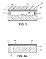
- FIG. 3 represents an encapsulation structure 300 according to a third embodiment.
- the encapsulation structure 300 comprises the cavity 110 formed between the first substrate 102 and the second substrate 112 and in which the device 108 and at least a portion of the integrated circuit 104 are encapsulated.
- the integrated circuit 104 is made on the first substrate 102 which forms the cover of the cavity 110.
- the device 108 is therefore not produced on the integrated circuit 104, but directly on and / or in the second substrate 112.
- the integrated circuit 104 is covered by the layer of getter material 106 for absorbing and / or adsorbing the gases released by the materials of the integrated circuit 104 during the thermal activation of the getter material present in the encapsulation structure 300
- the layer of getter material 106 it is possible for one or more portions of getter material, for example similar to the portion 206 previously described, to be made on the second substrate 112, beside the device 108, or on the first substrate 102, against the layer of getter material 106. It is also possible for another layer of getter material to be made on the second substrate 112, the device 108 being produced on this to be a layer of getter material. This other layer of getter material may be electrically isolated from the device 108 by a dielectric layer, for example similar to the passivation layer 115.
- an encapsulation structure comprises the first substrate 102 on which the integrated circuit 104 and the device 108 are made as shown in FIG. figure 1 and also comprises a second substrate, forming the cover, on which is also realized another integrated circuit covered with a layer of getter material.
- the encapsulation structures 100 and 200 have been previously described as encapsulating a single device 108, several devices can be encapsulated in each of the cavities 110 and 202 of the encapsulation structures 100 and 200. However, the encapsulation structures 100 and 200 are preferably made such that they individually encapsulate devices in a plurality of cavities collectively made between the first substrate 102 and the second substrate 112, and / or between the first substrate 102 and covers similar to the hood 204.
- the integrated circuit 104 is produced on the first substrate 102 by the implementation of conventional microelectronics steps.
- the integrated circuit 104 is then covered with the dielectric layer 111, in particular to electrically isolate the integrated circuit 104 from the layer of getter material 106 which will then be produced.
- the layer, or the stack of layers, of getter material 106 is then made as it covers, totally or partially, the integrated circuit 104.
- a dielectric passivation layer 115 for example composed of oxide and / or semiconductor nitride (for example silicon), can then be produced on the layer of getter material 106.
- the material or materials of this passivation layer 115 are preferably chosen such that they are the least favorable degassing after their achievements and when they are subjected to heat treatment.
- This passivation layer 115 is for example composed of SiO 2 deposited by evaporation (step which can be chained after the deposition of the layer of getter material 106 in the same deposition equipment).
- the passivation layer 115 may also be carried out by the implementation of oxidation and / or dry controlled nitriding of the getter material of the layer 106, thereby causing the growth of this oxide and / or nitride. Such oxidation and / or nitriding can be carried out at a temperature of between about 150 ° C. and 250 ° C. under a dry atmosphere of oxygen and / or of dinitrogen, at a pressure greater than or equal to about 10 -3 mbar for a few minutes. .
- the passivation layer 115 thus obtained corresponds to a metal oxide layer whose electrical characteristics give it both a hydrogen diffusion barrier role and an electrical insulating role with respect to the integrated circuit 104. This isolation Electrical advantage is advantageously reinforced by an insulation deposit such as SiO 2 .
- a heat treatment is then carried out, for example at a temperature of between approximately 300 ° C. and 450 ° C., advantageously under a secondary vacuum, for a duration of between a few minutes and approximately 1 hour.
- a heat treatment allows the layer of material getter 106 to trap the gases coming from the integrated circuit 104. Indeed, under the action of the temperature, the getter material is activated while the trapped gas escapes towards the outside of the integrated circuit 104. It also allows to degassing the passivation layer 115. The substrate is thus ready for subsequent technological steps.
- This heat treatment thus makes it possible to stabilize, with respect to its propensity to degass, the stack comprising the layer of getter material 106 and the passivation layer 115.
- a resumption of electrical contacts is then carried out on the integrated circuit 104.
- This resumption of contacts can be performed by the rear face of the integrated circuit 104, that is to say the face of the integrated circuit 104 lying against the substrate 102.
- one or more vias 118 are made through the substrate 102, forming one or more accesses to the rear face of the integrated circuit 104.
- An electrically conductive material is then deposited in this or these vias to form one or more electrical connections electrically connected to the integrated circuit 104.
- the device 108 is then made on the passivation layer 115, by implementing deposition steps, photolithography and etching.
- the cavity 110 is then closed by securing the second substrate 112 to the first substrate 102, the portion of getter material 116 being previously formed against the second substrate 112.
- the embodiment of the encapsulation structure 200 comprises the realization of the portion of getter material 206 on the passivation layer 115, next to the device 108.
- the cavity 202 is closed covering the device 108 and the portion of getter material 206 by a layer of sacrificial material which is then etched such that a remaining portion of sacrificial material corresponds to the desired volume of the cavity 202.
- the portion of sacrificial material is then covered with one or more thin layers (of which that lying against the portion of sacrificial material may be composed of getter material), forming the cover 204.
- the portion of sacrificial material is then etched via a release hole made through the cover 204, the hole is then plugged.
- the encapsulation structure 300 is obtained by producing the device 108 directly on the first substrate 102.
- the integrated circuit 104 is made on the second substrate 112, the integrated circuit 104 then being covered by the getter material layer 106 and possibly a passivation layer.
- the two substrates 102 and 112 are then secured to one another in order to close the cavity 110.
- the recovery of electrical contacts is performed through the second substrate 112.
- the encapsulation structure considered it is possible to carry out a resumption of electrical contacts at a front face of the integrated circuit 104, that is to say at the level of the face of the integrated circuit 104 lying on the side of the cavity.
- the getter material layer 106 after making the integrated circuit 104 covered with the getter material layer 106, the latter can be etched such that a remaining portion of getter material 106 covers the portion of the integrated circuit 104 intended to be encapsulated in the cavity with the device 108.
- the remaining portion of the getter material layer 106 may then be covered by the passivation layer 115, which also covers one or more portions of the integrated circuit 104 that are not intended to be exposed in the cavity.
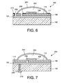
- the figure 5 represents the encapsulation structure 200 according to a first embodiment, wherein the recovery of electrical contacts is performed at the front face of the integrated circuit 104. It is seen in this figure that the integrated circuit 104 is electrically connected to the device 108 by a first electrical connection 208 which passes through the getter material layer 106, the passivation layer 115 and the dielectric layer 111.
- a second electrical connection 209 makes it possible to electrically contact the integrated circuit 104 from outside the cavity 202, this second link 209 passing through the passivation layer 115 to lead to the face before the encapsulation structure 200 and be connected to an electrical contact 210 formed on the front face.
- the electrical connections 208 and 209 are electrically isolated from the layer of getter material 106, for example by surrounding the electrically conductive material of these bonds with a dielectric material previously disposed in the holes formed through the layer of getter material 106 and the layer passivation 115.
- the figure 6 represents the encapsulation structure 200 according to a second variant embodiment.
- the electrical connection 208 is located next to the device 108 and has two parts perpendicular to each other, one being in the plane of the device 108, the other being in a plane perpendicular to the device 108 and through the layers 106, 111 and 115.
- the second electrical connection 209 passes through the substrate 102 to open on the rear face of the substrate 102 and to be in contact with an electrical contact 210 made at the rear face of the substrate 102.
Landscapes
- Engineering & Computer Science (AREA)
- Microelectronics & Electronic Packaging (AREA)
- Manufacturing & Machinery (AREA)
- Physics & Mathematics (AREA)
- Condensed Matter Physics & Semiconductors (AREA)
- General Physics & Mathematics (AREA)
- Computer Hardware Design (AREA)
- Power Engineering (AREA)
- Micromachines (AREA)
- Non-Metallic Protective Coatings For Printed Circuits (AREA)
Claims (20)
- Verkapselungsstruktur (100, 200, 300), umfassend wenigstens einen Hohlraum (110, 202), welcher zwischen einem ersten Substrat (102) und einer Abdeckung (112) gebildet ist, wobei der Hohlraum hermetisch abgeschlossen ist und wobei wenigstens verkapselt sind:- eine Vorrichtung (108),- eine zu einem integrierten Schaltkreis (104), welcher auf dem ersten Substrat (102) ausgebildet ist, zugehörige elektronische Komponente, und- eine Schicht aus einem Getter-Material (106), welche die elektronische Komponente integral derart bedeckt, dass von der elektronischen Komponente ausgasbare Gase blockiert werden,wobei folglich die elektronische Komponente nicht in dem Hohlraum offenliegt,
und wobei die Vorrichtung (108) nicht von der Schicht aus einem Getter-Material (106) bedeckt ist. - Verkapselungsstruktur (100, 200, 300) nach Anspruch 1, wobei die Vorrichtung (108) vom Typ eines MEMS oder/und NEMS oder/und MOEMS oder/und NOEMS oder/und eines Infrarot-Detektors ist oder/und wobei die elektronische Komponente ein Transistor vom MOS-Typ ist.
- Verkapselungsstruktur (100, 200, 300) nach einem der vorhergehenden Ansprüche, wobei die elektronische Komponente zu einem integrierten Schaltkreis (104), welcher auf dem ersten Substrat (102) gebildet ist, zugehörig ist und wenigstens ein Teil von ihr unter dem Hohlraum (110, 202) angeordnet ist.
- Verkapselungsstruktur (100, 200, 300) nach einem der vorhergehenden Ansprüche, ferner umfassend eine dielektrische Schicht (111), welche zwischen der elektronischen Komponente und der Schicht aus einem Getter-Material (106) angeordnet ist.
- Verkapselungsstruktur (100, 200, 300) nach einem der vorhergehenden Ansprüche, wobei der Hohlraum (110) zwischen dem ersten Substrat (102) und einem zweiten Substrat (112) gebildet ist, welches mit dem ersten Substrat (102) verbunden ist, oder zwischen dem ersten Substrat (102) und einer Abdeckung (204), welche eine oder mehrere dünne Schichten umfasst, welche mit dem ersten Substrat (102) verbunden sind.
- Verkapselungsstruktur (300) nach Anspruch 5, wobei die Vorrichtung (108) auf dem zweiten Substrat (112) ausgebildet ist.
- Verkapselungsstruktur (100, 200) nach einem der Ansprüche 1 bis 6, wobei die Vorrichtung (108) oberhalb der Schicht aus einem Getter-Material (106) ausgebildet ist.
- Verkapselungsstruktur (100, 200) nach Anspruch 7, ferner umfassend wenigstens eine Passivierungs-Schicht (115), welche zwischen der Schicht aus einem Getter-Material (106) und der Vorrichtung (108) angeordnet ist.
- Verkapselungsstruktur (200) nach einem der Ansprüche 7 oder 8, ferner umfassend wenigstens eine elektrische Verbindung (208), welche die Vorrichtung (108) mit der elektronischen Komponente durch die Schicht aus einem Getter-Material (106) hindurch elektrisch verbindet, sowie wenigstens eine zweite elektrische Verbindung (209), welche die elektronische Komponente mit wenigstens einem außerhalb des Hohlraums (202) angeordneten elektrischen Kontakt (210) verbindet, wobei die erste (208) und die zweite (209) elektrische Verbindung von der Schicht aus einem Getter-Material (106) elektrisch isoliert sind.
- Verkapselungsstruktur (100, 200) nach einem der vorhergehenden Ansprüche, ferner umfassend wenigstens einen von der Schicht aus einem Getter-Material (106) verschiedenen Abschnitt eines Getter-Materials (116, 206), welcher in dem Hohlraum (110, 202) angeordnet ist.
- Verkapselungsstruktur (100, 200, 300) nach einem der vorhergehenden Ansprüche, ferner umfassend eine oder mehrere elektrische Verbindungen (209), welche durch das erste Substrat (102) hindurch verlaufen und die elektronische Komponente mit einem oder mehreren elektrischen Kontakten (210) verbinden, welche außerhalb des Hohlraums (110, 202) angeordnet sind.
- Verkapselungsstruktur (100, 200, 300) nach einem der vorhergehenden Ansprüche, wobei die Schicht aus einem Getter-Material (106) einen Stapel umfasst, welcher aus wenigstens einer ersten Schicht, welche aus Titan besteht und die elektronische Komponente bedeckt, einer zweiten Schicht, welche aus Nickel besteht und die erste Schicht bedeckt, und einer dritten Schicht gebildet ist, welche aus Titan besteht und die zweite Schicht bedeckt.
- Verfahren zum Verkapseln wenigstens einer Vorrichtung (108) und wenigstens einer elektronischen Komponente in einem Hohlraum (110, 202), umfassend wenigstens die Schritte:- Ausbilden der einem integrierten Schaltkreis (104) zugeordneten elektronischen Komponente auf einem ersten Substrat (102);- Ausbilden wenigstens einer Schicht aus einem Getter-Material (106), welches die elektronische Komponente derart bedeckt, dass von der elektronischen Komponente ausgasbare Gase blockiert werden,- Ausbilden der Vorrichtung (108),- Hermetisches Schließen des Hohlraums (110, 202) durch eine Abdeckung (112), so dass die elektronische Komponente und die Vorrichtung (108) in dem Hohlraum (110, 202) verkapselt werden,wobei die elektronische Komponente folglich nicht in dem Hohlraum offenliegt,
wobei die Vorrichtung (108) nicht von der Schicht aus einem Getter-Material (106) bedeckt wird. - Verfahren zum Verkapseln nach Anspruch 13, wobei der Schritt des hermetischen Schließens des Hohlraums (110, 202) das Verbinden eines zweiten Substrats (112) mit dem ersten Substrat (102) umfasst, oder das Ausbilden einer Abdeckung (204), welche eine oder mehrere mit dem ersten Substrat (102) verbundene dünne Schichten umfasst.
- Verfahren zum Verkapseln nach Anspruch 14, wobei die Vorrichtung (108) auf dem zweiten Substrat (112) ausgebildet ist.
- Verfahren zum Verkapseln nach einem der Ansprüche 13 oder 14, wobei die Vorrichtung (108) oberhalb der Schicht aus einem Getter-Material (106) ausgebildet ist.
- Verfahren zum Verkapseln nach Anspruch 16, ferner umfassend, zwischen dem Schritt des Ausbildens der Schicht aus einem Getter-Material (106) und dem Schritt des Ausbildens der Vorrichtung (108), einen Schritt eines Ausbildens von wenigstens einer Passivierungs-Schicht (115) auf der Schicht aus einem Getter-Material (106), wobei die Vorrichtung (108) auf der Passivierungs-Schicht (115) ausgebildet wird.
- Verfahren zum Verkapseln nach einem der Schritte 16 oder 17, ferner umfassend, vor dem hermetischen Schließen des Hohlraums (110, 202), das Ausbilden von wenigstens einer ersten elektrischen Verbindung (208), welche die Vorrichtung (108) mit der elektronischen Komponente durch die Schicht aus einem Getter-Material (106) hindurch verbindet, sowie wenigstens einer zweiten elektrischen Verbindung (209), welche die elektronische Komponente mit wenigstens einem elektrischen Kontakt verbindet, welcher außerhalb des Hohlraums (110, 202) angeordnet ist, wobei die erste (208) und zweite (209) elektrische Verbindung von der Schicht aus einem Getter-Material (106) elektrisch isoliert ist.
- Verfahren zum Verkapseln nach einem der Ansprüche 13 bis 18, ferner umfassend, vor dem hermetischen Schließen des Hohlraums (110, 202), das Ausbilden wenigstens eines von der Schicht aus einem Getter-Material (106) verschiedenen Abschnitts eines Getter-Materials (116, 206), welcher in dem Hohlraum (110, 202) angeordnet ist.
- Verfahren zum Verkapseln nach einem der Ansprüche 13 bis 19, ferner umfassend das Ausbilden von einer oder mehreren elektrischen Verbindungen (209), welche durch das erste Substrat (102) hindurchtreten und die elektronische Komponente mit einem oder mehreren elektrischen Kontakten (210) verbinden, welche außerhalb des Hohlraums angeordnet sind.
Applications Claiming Priority (1)
| Application Number | Priority Date | Filing Date | Title |
|---|---|---|---|
| FR1159848A FR2982073B1 (fr) | 2011-10-28 | 2011-10-28 | Structure d'encapsulation hermetique d'un dispositif et d'un composant electronique |
Publications (3)
| Publication Number | Publication Date |
|---|---|
| EP2586741A2 EP2586741A2 (de) | 2013-05-01 |
| EP2586741A3 EP2586741A3 (de) | 2015-02-18 |
| EP2586741B1 true EP2586741B1 (de) | 2016-03-23 |
Family
ID=47018107
Family Applications (1)
| Application Number | Title | Priority Date | Filing Date |
|---|---|---|---|
| EP12189454.7A Active EP2586741B1 (de) | 2011-10-28 | 2012-10-22 | Hermetisch verschlossene Einkapselungsstruktur einer Vorrichtung und einer elektronischen Komponente |
Country Status (3)
| Country | Link |
|---|---|
| US (1) | US8884331B2 (de) |
| EP (1) | EP2586741B1 (de) |
| FR (1) | FR2982073B1 (de) |
Families Citing this family (8)
| Publication number | Priority date | Publication date | Assignee | Title |
|---|---|---|---|---|
| US8847373B1 (en) * | 2013-05-07 | 2014-09-30 | Innovative Micro Technology | Exothermic activation for high vacuum packaging |
| US9764946B2 (en) | 2013-10-24 | 2017-09-19 | Analog Devices, Inc. | MEMs device with outgassing shield |
| DE102013222583B4 (de) | 2013-11-07 | 2024-06-20 | Robert Bosch Gmbh | Mikromechanische Sensorvorrichtung und entsprechendes Herstellungsverfahren |
| FR3014241B1 (fr) | 2013-11-29 | 2017-05-05 | Commissariat Energie Atomique | Structure d'encapsulation comprenant des tranchees partiellement remplies de materiau getter |
| FR3023974B1 (fr) | 2014-07-18 | 2016-07-22 | Ulis | Procede de fabrication d'un dispositif comprenant un boitier hermetique sous vide et un getter |
| CN105366630B (zh) * | 2014-07-30 | 2018-03-30 | 中芯国际集成电路制造(上海)有限公司 | 一种半导体器件的制造方法和电子装置 |
| JP7009857B2 (ja) * | 2017-09-13 | 2022-01-26 | セイコーエプソン株式会社 | 液体噴射ヘッド、液体噴射装置、及び、圧電デバイス |
| DE102022210970A1 (de) | 2022-10-18 | 2024-04-18 | Robert Bosch Gesellschaft mit beschränkter Haftung | Mikromechanische Vorrichtung mit einer Wasserstoff-Drainage-Schicht |
Family Cites Families (21)
| Publication number | Priority date | Publication date | Assignee | Title |
|---|---|---|---|---|
| JP3100131B1 (ja) * | 1998-09-07 | 2000-10-16 | キヤノン株式会社 | 画像形成装置 |
| FR2816447B1 (fr) * | 2000-11-07 | 2003-01-31 | Commissariat Energie Atomique | Dispositif de detection de rayonnements electromagnetiques tridimensionnel et procede de realisation de ce dispositif |
| FR2822541B1 (fr) * | 2001-03-21 | 2003-10-03 | Commissariat Energie Atomique | Procedes et dispositifs de fabrication de detecteurs de rayonnement |
| FR2842022B1 (fr) * | 2002-07-03 | 2005-05-06 | Commissariat Energie Atomique | Dispositif de maintien d'un objet sous vide et procedes de fabrication de ce dispositif, application aux detecteurs intrarouges non refroidis |
| US20040189195A1 (en) | 2003-03-24 | 2004-09-30 | Osram Opto Semiconductors Gmbh | Devices including, methods using, and compositions of reflowable getters |
| JP2005241457A (ja) * | 2004-02-26 | 2005-09-08 | Hamamatsu Photonics Kk | 赤外線センサ及びその製造方法 |
| FR2883099B1 (fr) | 2005-03-14 | 2007-04-13 | Commissariat Energie Atomique | Protection d'un getter en couche mince |
| DE102006016260B4 (de) | 2006-04-06 | 2024-07-18 | Fraunhofer-Gesellschaft zur Förderung der angewandten Forschung e.V. | Vielfach-Bauelement mit mehreren aktive Strukturen enthaltenden Bauteilen (MEMS) zum späteren Vereinzeln, flächiges Substrat oder flächig ausgebildete Kappenstruktur, in der Mikrosystemtechnik einsetzbares Bauteil mit aktiven Strukturen, Einzelsubstrat oder Kappenstruktur mit aktiven Strukturen und Verfahren zum Herstellen eines Vielfach-Bauelements |
| FR2903678B1 (fr) | 2006-07-13 | 2008-10-24 | Commissariat Energie Atomique | Microcomposant encapsule equipe d'au moins un getter |
| US7659150B1 (en) * | 2007-03-09 | 2010-02-09 | Silicon Clocks, Inc. | Microshells for multi-level vacuum cavities |
| FR2922202B1 (fr) | 2007-10-15 | 2009-11-20 | Commissariat Energie Atomique | Structure comportant une couche getter et une sous-couche d'ajustement et procede de fabrication. |
| FR2925224B1 (fr) * | 2007-12-14 | 2010-06-18 | Commissariat Energie Atomique | Dispositif comportant un composant organique et une couche d'encapsulation avec un materiau reactif a l'humidite |
| FR2933390B1 (fr) * | 2008-07-01 | 2010-09-03 | Commissariat Energie Atomique | Procede d'encapsulation d'un dispositif microelectronique par un materiau getter |
| US8120155B2 (en) * | 2008-07-31 | 2012-02-21 | Texas Instruments Incorporated | Reduced stiction and mechanical memory in MEMS devices |
| FR2946777B1 (fr) * | 2009-06-12 | 2011-07-22 | Commissariat Energie Atomique | Dispositif de detection et/ou d'emission de rayonnement electromagnetique et procede de fabrication d'un tel dispositif |
| FR2947812B1 (fr) * | 2009-07-07 | 2012-02-10 | Commissariat Energie Atomique | Cavite etanche et procede de realisation d'une telle cavite etanche |
| FR2948928B1 (fr) * | 2009-08-06 | 2012-02-24 | Commissariat Energie Atomique | Structure a microcavite et structure d'encapsulation d'un dispositif microelectronique |
| FR2950876B1 (fr) * | 2009-10-07 | 2012-02-10 | Commissariat Energie Atomique | Procede de traitement d'un materiau getter et procede d'encapsulation d'un tel materiau getter |
| FR2950877B1 (fr) * | 2009-10-07 | 2012-01-13 | Commissariat Energie Atomique | Structure a cavite comportant une interface de collage a base de materiau getter |
| FR2952627A1 (fr) * | 2009-11-17 | 2011-05-20 | Commissariat Energie Atomique | Getter ayant deux temperatures d'activation et structure comportant ce getter |
| US9586811B2 (en) * | 2011-06-10 | 2017-03-07 | Taiwan Semiconductor Manufacturing Company, Ltd. | Semiconductor devices with moving members and methods for making the same |
-
2011
- 2011-10-28 FR FR1159848A patent/FR2982073B1/fr not_active Expired - Fee Related
-
2012
- 2012-10-22 EP EP12189454.7A patent/EP2586741B1/de active Active
- 2012-10-26 US US13/661,792 patent/US8884331B2/en active Active
Also Published As
| Publication number | Publication date |
|---|---|
| FR2982073B1 (fr) | 2014-10-10 |
| US20130105959A1 (en) | 2013-05-02 |
| FR2982073A1 (fr) | 2013-05-03 |
| EP2586741A3 (de) | 2015-02-18 |
| US8884331B2 (en) | 2014-11-11 |
| EP2586741A2 (de) | 2013-05-01 |
Similar Documents
| Publication | Publication Date | Title |
|---|---|---|
| EP2586741B1 (de) | Hermetisch verschlossene Einkapselungsstruktur einer Vorrichtung und einer elektronischen Komponente | |
| EP2308797B1 (de) | Struktur mit Hohlraum, die eine Bindungsschnittstelle auf der Basis eines Getter-Materials umfasst | |
| EP2450949B1 (de) | Einkapselungssstruktur einer Mikrovorrichtung, die ein Getter-Material umfasst | |
| EP2284121B1 (de) | Hohlraum für ein mikromechanisches Bauelement | |
| EP2637966B1 (de) | Verfahren zur herstellung eines substrats mit eingebetteten schichten aus fangstoff | |
| FR3021645B1 (fr) | Structure d'encapsulation a plusieurs cavites munies de canaux d'acces de hauteurs differentes | |
| FR2903678A1 (fr) | Microcomposant encapsule equipe d'au moins un getter | |
| EP2803634B1 (de) | Einkapselungsverfahren für eine mikroelektronische Vorrichtung mittels der Injektion von einem Edelgas durch ein Material, welches für dieses Edelgas durchlässig ist | |
| EP2628708B1 (de) | Mikroelektronisches Substrat mit einer vergrabenen Schicht organischem Materials | |
| EP3020684B1 (de) | Einkapselungsstruktur mit hohlraum der an einen aus einem durchlässigen material gebildeten gasinjektionskanal gekoppelt ist | |
| EP2897162B1 (de) | Einkapselungsstruktur, die teilweise mit Gettermaterial gefüllte Rinnen umfasst | |
| WO2004006290A2 (fr) | Dispositif de maintien d'un objet sous vide et procedes de fabrication de ce dispositif, application aux detecteurs infrarouges non refroidis | |
| EP3184486B1 (de) | Verfahren zur herstellung eines versiegelten mems-hohlraums mit einer klappe zum schützen des hohlraums während des verkapselungsvorgangs | |
| EP3165502B1 (de) | Mikroelektronische vorrichtung | |
| EP3034460B1 (de) | Mehrstufige getter-struktur und einkapselungsstruktur, die eine solche mehrstufige getter-struktur umfasst | |
| EP3173375A1 (de) | Einkapselungsverfahren einer mikroelektronischen vorrichtung mit einem auslassloch variabler grösse | |
| FR3103551A1 (fr) | Procédé de fabrication d’un dispositif de détection comportant une etape de collage direct d’une couche mince de scellement munie d’un matériau getter | |
| FR3074358A1 (fr) | Procede de realisation d'une cavite etanche a couche mince |
Legal Events
| Date | Code | Title | Description |
|---|---|---|---|
| PUAI | Public reference made under article 153(3) epc to a published international application that has entered the european phase |
Free format text: ORIGINAL CODE: 0009012 |
|
| AK | Designated contracting states |
Kind code of ref document: A2 Designated state(s): AL AT BE BG CH CY CZ DE DK EE ES FI FR GB GR HR HU IE IS IT LI LT LU LV MC MK MT NL NO PL PT RO RS SE SI SK SM TR |
|
| AX | Request for extension of the european patent |
Extension state: BA ME |
|
| PUAL | Search report despatched |
Free format text: ORIGINAL CODE: 0009013 |
|
| AK | Designated contracting states |
Kind code of ref document: A3 Designated state(s): AL AT BE BG CH CY CZ DE DK EE ES FI FR GB GR HR HU IE IS IT LI LT LU LV MC MK MT NL NO PL PT RO RS SE SI SK SM TR |
|
| AX | Request for extension of the european patent |
Extension state: BA ME |
|
| RIC1 | Information provided on ipc code assigned before grant |
Ipc: B81C 1/00 20060101AFI20150114BHEP Ipc: H01L 23/26 20060101ALI20150114BHEP |
|
| 17P | Request for examination filed |
Effective date: 20150727 |
|
| RBV | Designated contracting states (corrected) |
Designated state(s): AL AT BE BG CH CY CZ DE DK EE ES FI FR GB GR HR HU IE IS IT LI LT LU LV MC MK MT NL NO PL PT RO RS SE SI SK SM TR |
|
| GRAP | Despatch of communication of intention to grant a patent |
Free format text: ORIGINAL CODE: EPIDOSNIGR1 |
|
| INTG | Intention to grant announced |
Effective date: 20150916 |
|
| RIN1 | Information on inventor provided before grant (corrected) |
Inventor name: BAILLIN, XAVIER Inventor name: PORNIN, JEAN-LOUIS |
|
| GRAS | Grant fee paid |
Free format text: ORIGINAL CODE: EPIDOSNIGR3 |
|
| GRAA | (expected) grant |
Free format text: ORIGINAL CODE: 0009210 |
|
| AK | Designated contracting states |
Kind code of ref document: B1 Designated state(s): AL AT BE BG CH CY CZ DE DK EE ES FI FR GB GR HR HU IE IS IT LI LT LU LV MC MK MT NL NO PL PT RO RS SE SI SK SM TR |
|
| REG | Reference to a national code |
Ref country code: GB Ref legal event code: FG4D Free format text: NOT ENGLISH |
|
| REG | Reference to a national code |
Ref country code: CH Ref legal event code: EP |
|
| REG | Reference to a national code |
Ref country code: AT Ref legal event code: REF Ref document number: 782945 Country of ref document: AT Kind code of ref document: T Effective date: 20160415 |
|
| REG | Reference to a national code |
Ref country code: IE Ref legal event code: FG4D Free format text: LANGUAGE OF EP DOCUMENT: FRENCH |
|
| REG | Reference to a national code |
Ref country code: DE Ref legal event code: R096 Ref document number: 602012015886 Country of ref document: DE |
|
| REG | Reference to a national code |
Ref country code: LT Ref legal event code: MG4D |
|
| REG | Reference to a national code |
Ref country code: NL Ref legal event code: MP Effective date: 20160323 |
|
| PG25 | Lapsed in a contracting state [announced via postgrant information from national office to epo] |
Ref country code: FI Free format text: LAPSE BECAUSE OF FAILURE TO SUBMIT A TRANSLATION OF THE DESCRIPTION OR TO PAY THE FEE WITHIN THE PRESCRIBED TIME-LIMIT Effective date: 20160323 Ref country code: HR Free format text: LAPSE BECAUSE OF FAILURE TO SUBMIT A TRANSLATION OF THE DESCRIPTION OR TO PAY THE FEE WITHIN THE PRESCRIBED TIME-LIMIT Effective date: 20160323 Ref country code: GR Free format text: LAPSE BECAUSE OF FAILURE TO SUBMIT A TRANSLATION OF THE DESCRIPTION OR TO PAY THE FEE WITHIN THE PRESCRIBED TIME-LIMIT Effective date: 20160624 Ref country code: NO Free format text: LAPSE BECAUSE OF FAILURE TO SUBMIT A TRANSLATION OF THE DESCRIPTION OR TO PAY THE FEE WITHIN THE PRESCRIBED TIME-LIMIT Effective date: 20160623 |
|
| REG | Reference to a national code |
Ref country code: AT Ref legal event code: MK05 Ref document number: 782945 Country of ref document: AT Kind code of ref document: T Effective date: 20160323 |
|
| PG25 | Lapsed in a contracting state [announced via postgrant information from national office to epo] |
Ref country code: RS Free format text: LAPSE BECAUSE OF FAILURE TO SUBMIT A TRANSLATION OF THE DESCRIPTION OR TO PAY THE FEE WITHIN THE PRESCRIBED TIME-LIMIT Effective date: 20160323 Ref country code: SE Free format text: LAPSE BECAUSE OF FAILURE TO SUBMIT A TRANSLATION OF THE DESCRIPTION OR TO PAY THE FEE WITHIN THE PRESCRIBED TIME-LIMIT Effective date: 20160323 Ref country code: NL Free format text: LAPSE BECAUSE OF FAILURE TO SUBMIT A TRANSLATION OF THE DESCRIPTION OR TO PAY THE FEE WITHIN THE PRESCRIBED TIME-LIMIT Effective date: 20160323 Ref country code: LV Free format text: LAPSE BECAUSE OF FAILURE TO SUBMIT A TRANSLATION OF THE DESCRIPTION OR TO PAY THE FEE WITHIN THE PRESCRIBED TIME-LIMIT Effective date: 20160323 Ref country code: LT Free format text: LAPSE BECAUSE OF FAILURE TO SUBMIT A TRANSLATION OF THE DESCRIPTION OR TO PAY THE FEE WITHIN THE PRESCRIBED TIME-LIMIT Effective date: 20160323 |
|
| REG | Reference to a national code |
Ref country code: FR Ref legal event code: PLFP Year of fee payment: 5 |
|
| PG25 | Lapsed in a contracting state [announced via postgrant information from national office to epo] |
Ref country code: PL Free format text: LAPSE BECAUSE OF FAILURE TO SUBMIT A TRANSLATION OF THE DESCRIPTION OR TO PAY THE FEE WITHIN THE PRESCRIBED TIME-LIMIT Effective date: 20160323 Ref country code: EE Free format text: LAPSE BECAUSE OF FAILURE TO SUBMIT A TRANSLATION OF THE DESCRIPTION OR TO PAY THE FEE WITHIN THE PRESCRIBED TIME-LIMIT Effective date: 20160323 Ref country code: IS Free format text: LAPSE BECAUSE OF FAILURE TO SUBMIT A TRANSLATION OF THE DESCRIPTION OR TO PAY THE FEE WITHIN THE PRESCRIBED TIME-LIMIT Effective date: 20160723 |
|
| PG25 | Lapsed in a contracting state [announced via postgrant information from national office to epo] |
Ref country code: SK Free format text: LAPSE BECAUSE OF FAILURE TO SUBMIT A TRANSLATION OF THE DESCRIPTION OR TO PAY THE FEE WITHIN THE PRESCRIBED TIME-LIMIT Effective date: 20160323 Ref country code: SM Free format text: LAPSE BECAUSE OF FAILURE TO SUBMIT A TRANSLATION OF THE DESCRIPTION OR TO PAY THE FEE WITHIN THE PRESCRIBED TIME-LIMIT Effective date: 20160323 Ref country code: RO Free format text: LAPSE BECAUSE OF FAILURE TO SUBMIT A TRANSLATION OF THE DESCRIPTION OR TO PAY THE FEE WITHIN THE PRESCRIBED TIME-LIMIT Effective date: 20160323 Ref country code: CZ Free format text: LAPSE BECAUSE OF FAILURE TO SUBMIT A TRANSLATION OF THE DESCRIPTION OR TO PAY THE FEE WITHIN THE PRESCRIBED TIME-LIMIT Effective date: 20160323 Ref country code: AT Free format text: LAPSE BECAUSE OF FAILURE TO SUBMIT A TRANSLATION OF THE DESCRIPTION OR TO PAY THE FEE WITHIN THE PRESCRIBED TIME-LIMIT Effective date: 20160323 Ref country code: PT Free format text: LAPSE BECAUSE OF FAILURE TO SUBMIT A TRANSLATION OF THE DESCRIPTION OR TO PAY THE FEE WITHIN THE PRESCRIBED TIME-LIMIT Effective date: 20160725 Ref country code: ES Free format text: LAPSE BECAUSE OF FAILURE TO SUBMIT A TRANSLATION OF THE DESCRIPTION OR TO PAY THE FEE WITHIN THE PRESCRIBED TIME-LIMIT Effective date: 20160323 |
|
| PG25 | Lapsed in a contracting state [announced via postgrant information from national office to epo] |
Ref country code: IT Free format text: LAPSE BECAUSE OF FAILURE TO SUBMIT A TRANSLATION OF THE DESCRIPTION OR TO PAY THE FEE WITHIN THE PRESCRIBED TIME-LIMIT Effective date: 20160323 |
|
| REG | Reference to a national code |
Ref country code: DE Ref legal event code: R097 Ref document number: 602012015886 Country of ref document: DE |
|
| PLBE | No opposition filed within time limit |
Free format text: ORIGINAL CODE: 0009261 |
|
| STAA | Information on the status of an ep patent application or granted ep patent |
Free format text: STATUS: NO OPPOSITION FILED WITHIN TIME LIMIT |
|
| PG25 | Lapsed in a contracting state [announced via postgrant information from national office to epo] |
Ref country code: DK Free format text: LAPSE BECAUSE OF FAILURE TO SUBMIT A TRANSLATION OF THE DESCRIPTION OR TO PAY THE FEE WITHIN THE PRESCRIBED TIME-LIMIT Effective date: 20160323 |
|
| PG25 | Lapsed in a contracting state [announced via postgrant information from national office to epo] |
Ref country code: BE Free format text: LAPSE BECAUSE OF NON-PAYMENT OF DUE FEES Effective date: 20161031 Ref country code: BG Free format text: LAPSE BECAUSE OF FAILURE TO SUBMIT A TRANSLATION OF THE DESCRIPTION OR TO PAY THE FEE WITHIN THE PRESCRIBED TIME-LIMIT Effective date: 20160623 |
|
| 26N | No opposition filed |
Effective date: 20170102 |
|
| PG25 | Lapsed in a contracting state [announced via postgrant information from national office to epo] |
Ref country code: SI Free format text: LAPSE BECAUSE OF FAILURE TO SUBMIT A TRANSLATION OF THE DESCRIPTION OR TO PAY THE FEE WITHIN THE PRESCRIBED TIME-LIMIT Effective date: 20160323 |
|
| REG | Reference to a national code |
Ref country code: CH Ref legal event code: PL |
|
| REG | Reference to a national code |
Ref country code: IE Ref legal event code: MM4A |
|
| PG25 | Lapsed in a contracting state [announced via postgrant information from national office to epo] |
Ref country code: CH Free format text: LAPSE BECAUSE OF NON-PAYMENT OF DUE FEES Effective date: 20161031 Ref country code: LI Free format text: LAPSE BECAUSE OF NON-PAYMENT OF DUE FEES Effective date: 20161031 |
|
| PG25 | Lapsed in a contracting state [announced via postgrant information from national office to epo] |
Ref country code: LU Free format text: LAPSE BECAUSE OF NON-PAYMENT OF DUE FEES Effective date: 20161022 |
|
| REG | Reference to a national code |
Ref country code: FR Ref legal event code: PLFP Year of fee payment: 6 |
|
| PG25 | Lapsed in a contracting state [announced via postgrant information from national office to epo] |
Ref country code: IE Free format text: LAPSE BECAUSE OF NON-PAYMENT OF DUE FEES Effective date: 20161022 |
|
| REG | Reference to a national code |
Ref country code: BE Ref legal event code: MM Effective date: 20161031 |
|
| PG25 | Lapsed in a contracting state [announced via postgrant information from national office to epo] |
Ref country code: HU Free format text: LAPSE BECAUSE OF FAILURE TO SUBMIT A TRANSLATION OF THE DESCRIPTION OR TO PAY THE FEE WITHIN THE PRESCRIBED TIME-LIMIT; INVALID AB INITIO Effective date: 20121022 Ref country code: CY Free format text: LAPSE BECAUSE OF FAILURE TO SUBMIT A TRANSLATION OF THE DESCRIPTION OR TO PAY THE FEE WITHIN THE PRESCRIBED TIME-LIMIT Effective date: 20160323 |
|
| PG25 | Lapsed in a contracting state [announced via postgrant information from national office to epo] |
Ref country code: TR Free format text: LAPSE BECAUSE OF FAILURE TO SUBMIT A TRANSLATION OF THE DESCRIPTION OR TO PAY THE FEE WITHIN THE PRESCRIBED TIME-LIMIT Effective date: 20160323 Ref country code: MK Free format text: LAPSE BECAUSE OF FAILURE TO SUBMIT A TRANSLATION OF THE DESCRIPTION OR TO PAY THE FEE WITHIN THE PRESCRIBED TIME-LIMIT Effective date: 20160323 Ref country code: MC Free format text: LAPSE BECAUSE OF FAILURE TO SUBMIT A TRANSLATION OF THE DESCRIPTION OR TO PAY THE FEE WITHIN THE PRESCRIBED TIME-LIMIT Effective date: 20160323 Ref country code: MT Free format text: LAPSE BECAUSE OF FAILURE TO SUBMIT A TRANSLATION OF THE DESCRIPTION OR TO PAY THE FEE WITHIN THE PRESCRIBED TIME-LIMIT Effective date: 20160323 |
|
| REG | Reference to a national code |
Ref country code: FR Ref legal event code: PLFP Year of fee payment: 7 |
|
| PG25 | Lapsed in a contracting state [announced via postgrant information from national office to epo] |
Ref country code: AL Free format text: LAPSE BECAUSE OF FAILURE TO SUBMIT A TRANSLATION OF THE DESCRIPTION OR TO PAY THE FEE WITHIN THE PRESCRIBED TIME-LIMIT Effective date: 20160323 |
|
| PGFP | Annual fee paid to national office [announced via postgrant information from national office to epo] |
Ref country code: GB Payment date: 20231025 Year of fee payment: 12 |
|
| PGFP | Annual fee paid to national office [announced via postgrant information from national office to epo] |
Ref country code: FR Payment date: 20231023 Year of fee payment: 12 Ref country code: DE Payment date: 20231018 Year of fee payment: 12 |