EP2581952A2 - Light emitting diode, light emitting diode package and lighting apparatus including the same - Google Patents
Light emitting diode, light emitting diode package and lighting apparatus including the same Download PDFInfo
- Publication number
- EP2581952A2 EP2581952A2 EP12162167.6A EP12162167A EP2581952A2 EP 2581952 A2 EP2581952 A2 EP 2581952A2 EP 12162167 A EP12162167 A EP 12162167A EP 2581952 A2 EP2581952 A2 EP 2581952A2
- Authority
- EP
- European Patent Office
- Prior art keywords
- layer
- light emitting
- conductivity
- electrode
- type semiconductor
- Prior art date
- Legal status (The legal status is an assumption and is not a legal conclusion. Google has not performed a legal analysis and makes no representation as to the accuracy of the status listed.)
- Withdrawn
Links
Images







Classifications
-
- H—ELECTRICITY
- H10—SEMICONDUCTOR DEVICES; ELECTRIC SOLID-STATE DEVICES NOT OTHERWISE PROVIDED FOR
- H10W—GENERIC PACKAGES, INTERCONNECTIONS, CONNECTORS OR OTHER CONSTRUCTIONAL DETAILS OF DEVICES COVERED BY CLASS H10
- H10W90/00—Package configurations
-
- H—ELECTRICITY
- H10—SEMICONDUCTOR DEVICES; ELECTRIC SOLID-STATE DEVICES NOT OTHERWISE PROVIDED FOR
- H10H—INORGANIC LIGHT-EMITTING SEMICONDUCTOR DEVICES HAVING POTENTIAL BARRIERS
- H10H20/00—Individual inorganic light-emitting semiconductor devices having potential barriers, e.g. light-emitting diodes [LED]
- H10H20/80—Constructional details
- H10H20/83—Electrodes
-
- H—ELECTRICITY
- H10—SEMICONDUCTOR DEVICES; ELECTRIC SOLID-STATE DEVICES NOT OTHERWISE PROVIDED FOR
- H10H—INORGANIC LIGHT-EMITTING SEMICONDUCTOR DEVICES HAVING POTENTIAL BARRIERS
- H10H20/00—Individual inorganic light-emitting semiconductor devices having potential barriers, e.g. light-emitting diodes [LED]
- H10H20/80—Constructional details
- H10H20/81—Bodies
- H10H20/819—Bodies characterised by their shape, e.g. curved or truncated substrates
-
- H—ELECTRICITY
- H10—SEMICONDUCTOR DEVICES; ELECTRIC SOLID-STATE DEVICES NOT OTHERWISE PROVIDED FOR
- H10H—INORGANIC LIGHT-EMITTING SEMICONDUCTOR DEVICES HAVING POTENTIAL BARRIERS
- H10H20/00—Individual inorganic light-emitting semiconductor devices having potential barriers, e.g. light-emitting diodes [LED]
- H10H20/80—Constructional details
- H10H20/83—Electrodes
- H10H20/831—Electrodes characterised by their shape
-
- H—ELECTRICITY
- H10—SEMICONDUCTOR DEVICES; ELECTRIC SOLID-STATE DEVICES NOT OTHERWISE PROVIDED FOR
- H10H—INORGANIC LIGHT-EMITTING SEMICONDUCTOR DEVICES HAVING POTENTIAL BARRIERS
- H10H20/00—Individual inorganic light-emitting semiconductor devices having potential barriers, e.g. light-emitting diodes [LED]
- H10H20/80—Constructional details
- H10H20/83—Electrodes
- H10H20/831—Electrodes characterised by their shape
- H10H20/8312—Electrodes characterised by their shape extending at least partially through the bodies
-
- H—ELECTRICITY
- H10—SEMICONDUCTOR DEVICES; ELECTRIC SOLID-STATE DEVICES NOT OTHERWISE PROVIDED FOR
- H10H—INORGANIC LIGHT-EMITTING SEMICONDUCTOR DEVICES HAVING POTENTIAL BARRIERS
- H10H20/00—Individual inorganic light-emitting semiconductor devices having potential barriers, e.g. light-emitting diodes [LED]
- H10H20/80—Constructional details
- H10H20/83—Electrodes
- H10H20/832—Electrodes characterised by their material
- H10H20/835—Reflective materials
-
- H—ELECTRICITY
- H10—SEMICONDUCTOR DEVICES; ELECTRIC SOLID-STATE DEVICES NOT OTHERWISE PROVIDED FOR
- H10H—INORGANIC LIGHT-EMITTING SEMICONDUCTOR DEVICES HAVING POTENTIAL BARRIERS
- H10H20/00—Individual inorganic light-emitting semiconductor devices having potential barriers, e.g. light-emitting diodes [LED]
- H10H20/80—Constructional details
- H10H20/84—Coatings, e.g. passivation layers or antireflective coatings
-
- H—ELECTRICITY
- H10—SEMICONDUCTOR DEVICES; ELECTRIC SOLID-STATE DEVICES NOT OTHERWISE PROVIDED FOR
- H10H—INORGANIC LIGHT-EMITTING SEMICONDUCTOR DEVICES HAVING POTENTIAL BARRIERS
- H10H20/00—Individual inorganic light-emitting semiconductor devices having potential barriers, e.g. light-emitting diodes [LED]
- H10H20/80—Constructional details
- H10H20/85—Packages
- H10H20/857—Interconnections, e.g. lead-frames, bond wires or solder balls
-
- H—ELECTRICITY
- H10—SEMICONDUCTOR DEVICES; ELECTRIC SOLID-STATE DEVICES NOT OTHERWISE PROVIDED FOR
- H10H—INORGANIC LIGHT-EMITTING SEMICONDUCTOR DEVICES HAVING POTENTIAL BARRIERS
- H10H20/00—Individual inorganic light-emitting semiconductor devices having potential barriers, e.g. light-emitting diodes [LED]
- H10H20/80—Constructional details
- H10H20/85—Packages
- H10H20/858—Means for heat extraction or cooling
-
- F—MECHANICAL ENGINEERING; LIGHTING; HEATING; WEAPONS; BLASTING
- F21—LIGHTING
- F21K—NON-ELECTRIC LIGHT SOURCES USING LUMINESCENCE; LIGHT SOURCES USING ELECTROCHEMILUMINESCENCE; LIGHT SOURCES USING CHARGES OF COMBUSTIBLE MATERIAL; LIGHT SOURCES USING SEMICONDUCTOR DEVICES AS LIGHT-GENERATING ELEMENTS; LIGHT SOURCES NOT OTHERWISE PROVIDED FOR
- F21K9/00—Light sources using semiconductor devices as light-generating elements, e.g. using light-emitting diodes [LED] or lasers
- F21K9/20—Light sources comprising attachment means
- F21K9/23—Retrofit light sources for lighting devices with a single fitting for each light source, e.g. for substitution of incandescent lamps with bayonet or threaded fittings
-
- F—MECHANICAL ENGINEERING; LIGHTING; HEATING; WEAPONS; BLASTING
- F21—LIGHTING
- F21V—FUNCTIONAL FEATURES OR DETAILS OF LIGHTING DEVICES OR SYSTEMS THEREOF; STRUCTURAL COMBINATIONS OF LIGHTING DEVICES WITH OTHER ARTICLES, NOT OTHERWISE PROVIDED FOR
- F21V29/00—Protecting lighting devices from thermal damage; Cooling or heating arrangements specially adapted for lighting devices or systems
- F21V29/50—Cooling arrangements
- F21V29/70—Cooling arrangements characterised by passive heat-dissipating elements, e.g. heat-sinks
- F21V29/83—Cooling arrangements characterised by passive heat-dissipating elements, e.g. heat-sinks the elements having apertures, ducts or channels, e.g. heat radiation holes
-
- F—MECHANICAL ENGINEERING; LIGHTING; HEATING; WEAPONS; BLASTING
- F21—LIGHTING
- F21Y—INDEXING SCHEME ASSOCIATED WITH SUBCLASSES F21K, F21L, F21S and F21V, RELATING TO THE FORM OR THE KIND OF THE LIGHT SOURCES OR OF THE COLOUR OF THE LIGHT EMITTED
- F21Y2115/00—Light-generating elements of semiconductor light sources
- F21Y2115/10—Light-emitting diodes [LED]
-
- H—ELECTRICITY
- H10—SEMICONDUCTOR DEVICES; ELECTRIC SOLID-STATE DEVICES NOT OTHERWISE PROVIDED FOR
- H10H—INORGANIC LIGHT-EMITTING SEMICONDUCTOR DEVICES HAVING POTENTIAL BARRIERS
- H10H20/00—Individual inorganic light-emitting semiconductor devices having potential barriers, e.g. light-emitting diodes [LED]
- H10H20/01—Manufacture or treatment
- H10H20/011—Manufacture or treatment of bodies, e.g. forming semiconductor layers
- H10H20/018—Bonding of wafers
-
- H—ELECTRICITY
- H10—SEMICONDUCTOR DEVICES; ELECTRIC SOLID-STATE DEVICES NOT OTHERWISE PROVIDED FOR
- H10H—INORGANIC LIGHT-EMITTING SEMICONDUCTOR DEVICES HAVING POTENTIAL BARRIERS
- H10H20/00—Individual inorganic light-emitting semiconductor devices having potential barriers, e.g. light-emitting diodes [LED]
- H10H20/80—Constructional details
- H10H20/81—Bodies
- H10H20/819—Bodies characterised by their shape, e.g. curved or truncated substrates
- H10H20/82—Roughened surfaces, e.g. at the interface between epitaxial layers
-
- H—ELECTRICITY
- H10—SEMICONDUCTOR DEVICES; ELECTRIC SOLID-STATE DEVICES NOT OTHERWISE PROVIDED FOR
- H10H—INORGANIC LIGHT-EMITTING SEMICONDUCTOR DEVICES HAVING POTENTIAL BARRIERS
- H10H20/00—Individual inorganic light-emitting semiconductor devices having potential barriers, e.g. light-emitting diodes [LED]
- H10H20/80—Constructional details
- H10H20/83—Electrodes
- H10H20/831—Electrodes characterised by their shape
- H10H20/8316—Multi-layer electrodes comprising at least one discontinuous layer
-
- H—ELECTRICITY
- H10—SEMICONDUCTOR DEVICES; ELECTRIC SOLID-STATE DEVICES NOT OTHERWISE PROVIDED FOR
- H10H—INORGANIC LIGHT-EMITTING SEMICONDUCTOR DEVICES HAVING POTENTIAL BARRIERS
- H10H20/00—Individual inorganic light-emitting semiconductor devices having potential barriers, e.g. light-emitting diodes [LED]
- H10H20/80—Constructional details
- H10H20/85—Packages
- H10H20/8506—Containers
Definitions
- Embodiments relate to a light emitting device, a light emitting device package and a lighting apparatus including the same.
- Light emitting devices such as light emitting diodes (LEDs) and laser diodes (LDs), which use a Group III-V or Group II-VI compound semiconductor material, may render various colors such as red, green, blue, and ultraviolet by virtue of development of thin film growth technologies and device materials. It may also be possible to produce white light at high efficiency using fluorescent materials or through color mixing. Further, the light emitting devices have advantages, such as low power consumption, semi-permanent lifespan, fast response time, safety, and environmental friendliness as compared to conventional light sources, such as fluorescent lamps and incandescent lamps.
- these light emitting elements are increasingly applied to transmission modules of optical communication units, light emitting diode backlights as a replacement for cold cathode fluorescent lamps (CCFLs) constituting backlights of liquid crystal display (LCD) devices, and lighting apparatuses using white light emitting diodes as a replacement for fluorescent lamps or incandescent lamps, headlights for vehicles and traffic lights.
- CCFLs cold cathode fluorescent lamps
- LCD liquid crystal display
- the thickness thereof is greater than that of a light emitting device having a semiconductor layer with a general thickness. For this reason, the length of a path, along which light generated from an active layer travels before being outwardly emitted, is long, so that the amount of light absorbed in the semiconductor layer disposed over the active layer increases. As a result, the light extraction efficiency of the light emitting device may be degraded.
- Embodiments achieve an enhancement in the light extraction efficiency of a light emitting device through a reduction in the thickness of a semiconductor layer included in the light emitting device.
- a light emitting device includes a light emitting structure including a first-conductivity-type semiconductor layer, an active layer, and a second-conductivity-type semiconductor layer, a second electrode layer disposed beneath the light emitting structure and electrically connected to the second-conductivity-type semiconductor layer, a first electrode layer including a main electrode disposed beneath the second electrode layer, and at least one contact electrode branching from the main electrode and extending through the second electrode layer, the second-conductivity-type semiconductor layer and the active layer, to contact the first-conductivity-type semiconductor layer, and an insulating layer interposed between the first electrode layer and the second electrode layer and between the first electrode layer and the light emitting structure, wherein the first-conductivity-type semiconductor layer includes a first region and a second region having a smaller height than the first region, and the first region overlaps with the contact electrode.
- a light emitting device in another embodiment, includes a light emitting structure including a first-conductivity-type semiconductor layer, an active layer, and a second-conductivity-type semiconductor layer, which are stacked in a predetermined direction, a second electrode layer disposed beneath the light emitting structure and electrically connected to the second-conductivity-type semiconductor layer, a first electrode layer including a main electrode disposed beneath the second electrode layer, and at least one contact electrode branching from the main electrode and extending through the second electrode layer, the second-conductivity-type semiconductor layer and the active layer, to contact the first-conductivity-type semiconductor layer, and an insulating layer interposed between the first electrode layer and the second electrode layer and between the first electrode layer and the light emitting structure, wherein the first-conductivity-type semiconductor layer includes a first region and a second region having a smaller thickness than the first region, and the first region overlaps with the contact electrode in the predetermined direction.
- the first region may have a width equal to or greater than a width of the contact electrode.
- the width of the first region may correspond to 1 to 5 times the width of the contact electrode.
- a roughness or a pattern may be formed at an upper surface of the first-conductivity-type semiconductor layer.
- the light emitting device may further include a passivation layer formed on side surfaces of the light emitting structure, to cover at least a portion of the second-conductivity-type semiconductor layer, at least a portion of the active layer, and at least a portion of the first-conductivity-type semiconductor layer.
- a roughness may be formed at a portion of the contact electrode contacting the first-conductivity-type semiconductor layer.
- a portion of the second electrode layer may be exposed outside the light emitting structure, and an electrode pad may be formed on the exposed portion of the second electrode layer.
- the second electrode layer may include an ohmic layer and/or a reflective layer disposed beneath the second-conductivity-type semiconductor layer.
- the second electrode layer may include a current spreading layer, and the electrode pad may be disposed to contact the current spreading layer.
- the light emitting device may further include a passivation layer formed on side surfaces of the first region.
- the first region may have at least one of a stripe shape, a circular prism shape, a conical shape, a pyramid shape, a square prism shape, and a hemi-spherical shape.
- a light emitting device package comprises a body; first and second lead frames mounted on the body; and a light emitting device which is mounted on the body and electrically connected to the first and second lead frames, wherein the light emitting device comprises a light emitting structure comprising a first-conductivity-type semiconductor layer, an active layer, and a second-conductivity-type semiconductor layer, which are stacked in a predetermined direction; a second electrode layer disposed beneath the light emitting structure and electrically connected to the second-conductivity-type semiconductor layer; a first electrode layer comprising a main electrode disposed beneath the second electrode layer, and at least one contact electrode branching from the main electrode and extending through the second electrode layer, the second-conductivity-type semiconductor layer and the active layer, to contact the first-conductivity-type semiconductor layer; and an insulating layer interposed between the first electrode layer and the second electrode layer and between the first electrode layer and the light emitting structure, and wherein the first-conductivity-type semiconductor layer comprises a first region and
- a lighting apparatus in another embodiment, includes a light source for emitting light, the light source including a plurality of light emitting device packages mounted on a circuit board, a housing, in which the light source is mounted, a heat dissipation unit to dissipate heat generated from the light source, and a holder for coupling the light source and the heat dissipation unit to the housing, wherein each of the light emitting device packages includes a body, first and second lead frames disposed on the body, and a light emitting device disposed on the body and electrically connected to the first and second lead frames, wherein the light emitting device includes a light emitting structure including a first-conductivity-type semiconductor layer, an active layer, and a second-conductivity-type semiconductor layer, which are stacked in a predetermined direction, a second electrode layer disposed beneath the light emitting structure and electrically connected to the second-conductivity-type semiconductor layer, a first electrode layer including a main electrode disposed beneath the second electrode layer, and at least one contact
- each layer is exaggerated, omitted, or schematically illustrated for convenience of description and clarity. Also, the size or area of each constituent element does not entirely reflect the actual size thereof.
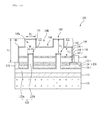
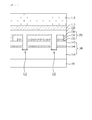
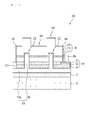
- FIG. 1A is a sectional view illustrating a light emitting device according to an exemplary embodiment.
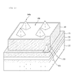
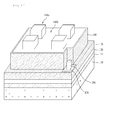
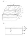
- FIGs. 1B to 1G are perspective views illustrating light emitting devices according to various embodiments, respectively.
- the light emitting device includes a support substrate 110, a first electrode layer 120 disposed over the support substrate 110, a second electrode layer 130 disposed over the first electrode layer 120, and a light emitting structure 140 disposed over the second electrode layer 130.
- the light emitting structure 140 includes a first-conductivity-type semiconductor layer 146, an active layer 144, and a second-conductivity-type semiconductor layer 142, which are stacked in a same direction.
- the light emitting device 100 may include a light emitting diode (LED) using a plurality of compound semiconductor layers, for example, semiconductor layers made of Group III-V elements.
- the LED may be a colored LED to emit blue, green, or red light, or an ultraviolet (UV) LED, although the present disclosure is not limited thereto. Emission of light from the LED may be achieved using various semiconductors, although the present disclosure is not limited thereto.
- the light emitting structure 140 may be formed using, for example, metal organic chemical vapor deposition (MOCVD), chemical vapor deposition (CVD), plasma-enhanced chemical vapor deposition (PECVD), molecular beam epitaxy (MBE), hydride vapor phase epitaxy (HVPE), or the like.
- MOCVD metal organic chemical vapor deposition
- CVD chemical vapor deposition
- PECVD plasma-enhanced chemical vapor deposition
- MBE molecular beam epitaxy
- HVPE hydride vapor phase epitaxy
- the first-conductivity-type semiconductor layer 146 may be made of a semiconductor compound, for example, a Group III-V or Group II-VI compound semiconductor.
- the first-conductivity-type semiconductor layer 146 may be doped with a first-conductivity-type dopant.
- the first-conductivity-type semiconductor layer 146 is an n-type semiconductor layer, the first-conductivity-type dopant is an n-type dopant.
- the n-type dopant may include Si, Ge, Sn, Se, or Te, although the present disclosure is not limited thereto.
- the first-conductivity-type semiconductor layer 146 is a p-type semiconductor layer, the first-conductivity-type dopant is a p-type dopant.
- the p-type dopant may include Mg, Zn, Ca, Sr, Ba, or the like, although the present disclosure is not limited thereto.
- the first-conductivity-type semiconductor layer 146 may include a semiconductor material having a formula of Al x In y Ga 1-x-y N (0 ⁇ x ⁇ 1, 0 ⁇ y ⁇ 1, and 0 ⁇ x+y ⁇ 1).
- the first-conductivity-type semiconductor layer 146 may be made of at least one of GaN, InN, AlN, InGaN, AlGaN, InAlGaN, AlInN, AlGaAs, InGaAs, AlInGaAs, GaP, AlGaP, InGaP, AlInGaP, and InP.
- a roughness or pattern 160 may be formed on an upper surface of the first-conductivity-type semiconductor layer 146.
- the active layer 144 In the active layer 144, electrons and holes meet, thereby emitting light with energy determined by the intrinsic energy band of the material of the active layer 144 (light emitting layer).
- the active layer 144 may have at least one of a single quantum well structure, a multi quantum well structure, a quantum wire structure, and a quantum dot structure.
- the active layer 144 may have a multi quantum well structure through injection of tri-methyl gallium gas (TMGa), ammonia gas (NH 3 ), nitrogen gas (N 2 ), and tri-methyl indium gas (TMIn), although the present disclosure is not limited thereto.
- TMGa tri-methyl gallium gas
- NH 3 ammonia gas
- N 2 nitrogen gas
- TIn tri-methyl indium gas
- the active layer 144 may have well and barrier layers having a layer pair structure made of at least one of InGaN/GaN, InGaN/InGaN, GaN/AlGaN, InAlGaN/GaN, GaAs(InGaAs)/AlGaAs, and GaP(InGaP)/AlGaP, although the present disclosure is not limited thereto.
- the well layer may be made of a material having a narrower band gap than the barrier layer.
- a conductive clad layer may be formed over and/or beneath the active layer 144.
- the conductive clad layer may be made of a semiconductor having a wider bandgap than the barrier layer of the active layer 144.
- the conductive clad layer may be made of GaN, AlGaN or InAlGaN, or may have a super-lattice structure.
- the conductive clad layer may be doped with a dopant to have an n-type or p-type conductivity.
- the second-conductivity-type semiconductor layer 142 may be made of a semiconductor compound, for example, a Group III-V compound semiconductor doped with a second-conductivity-type dopant.
- the second-conductivity-type semiconductor layer 142 may include a semiconductor material having a formula of In x Al y Ga 1-x-y N (0 ⁇ x ⁇ 1, 0 ⁇ y ⁇ 1, 0 ⁇ x + y ⁇ 1).
- the second-conductivity-type semiconductor layer 142 is a p-type semiconductor layer
- the second-conductivity-type dopant is a p-type dopant.
- the p-type dopant may include Mg, Zn, Ca, Sr, Ba, or the like, although the present disclosure is not limited thereto.
- the second-conductivity-type semiconductor layer 142 is an n-type semiconductor layer
- the second-conductivity-type dopant is an n-type dopant.
- the n-type dopant may include Si, Ge, Sn, Se, or Te, although the present disclosure is not limited thereto.
- the first semiconductor layer 146 may be implemented as an n-type semiconductor layer, and the second semiconductor layer 142 may be implemented as a p-type semiconductor layer.
- the first semiconductor layer 146 may be implemented as a p-type semiconductor layer
- the second semiconductor layer 142 may be implemented as an n-type semiconductor layer.
- a semiconductor layer having an opposite polarity to the second conduction type may be formed.
- an n-type semiconductor layer (not shown) may be formed over the second-conduction-type semiconductor layer 142.
- the light emitting structure 140 may be implemented as one of an n-p junction structure, a p-n junction structure, an n-p-n junction structure, and a p-n-p junction structure.
- the support substrate 110 supports the light emitting structure 140.
- the support substrate 110 may be a conductive substrate or an insulating substrate.
- the support substrate 110 may be made of a material having high electrical conductivity and high thermal conductivity.
- the support substrate 110 may be formed as a base substrate having a certain thickness, using a material selected from the group consisting of molybdenum (Mo), silicon (Si), tungsten (W), copper (Cu), aluminum (Al), and alloys thereof.
- the support substrate 110 may selectively include gold (Au), a Cu alloy, Ni, Cu-W, a carrier wafer (for example, GaN, Si, Ge, GaAs, ZnO, SiGe, SiC, SiGe, Ga 2 O 3 , or the like), a conductive sheet, or the like.
- Au gold
- a Cu alloy for example, GaN, Si, Ge, GaAs, ZnO, SiGe, SiC, SiGe, Ga 2 O 3 , or the like
- a conductive sheet for example, GaN, Si, Ge, GaAs, ZnO, SiGe, SiC, SiGe, Ga 2 O 3 , or the like.
- the first electrode layer 120 is formed over the support substrate 110.
- the first electrode layer 120 may be made of a metal.
- the first electrode layer 120 may include at least one of an ohmic layer, a reflective layer, and a bonding layer.
- the first electrode layer 120 may come into ohmic contact with a first semiconductor layer 146, which will be described later, using a reflective metal or a conductive oxide.
- the first electrode layer 120 may be made of Ag, Ni, Al, Rh, Pd, Ir, Ru, Mg, Zn, Pt, Au, Hf, or a selective combination thereof.
- the first electrode layer 120 may be formed to have a single layer structure or a multilayer structure, using a reflective electrode material having ohmic characteristics. When the first electrode layer 120 performs an ohmic function, the ohmic layer may be dispensed with.
- the first electrode layer 120 may be made of at least one of indium tin oxide (ITO), indium zinc oxide (IZO), indium zinc tin oxide (IZTO), indium aluminum zinc oxide (IAZO), indium gallium zinc oxide (IGZO), indium gallium tin oxide (IGTO), aluminum zinc oxide (AZO), antimony tin oxide (ATO), gallium zinc oxide (GZO), IrO x , RuO x , NiO, RuO x /ITO, Ni/IrO x /Au, and Ni/IrO x /Au/ITO, although the present disclosure is not limited thereto.
- ITO indium tin oxide
- IZO indium zinc oxide
- IZTO indium aluminum zinc oxide
- IGZO indium gallium zinc oxide
- IGTO indium gallium tin oxide
- ATO antimony tin oxide
- GZO gallium zinc oxide
- the first electrode layer 120 may include a bonding layer.
- the bonding layer may include a barrier metal or a bonding metal.
- the bonding layer may include at least one of Ti, Au, Sn, Ni, Cr, Ga, In, Bi, Cu, Ag, and Ta.
- a separate bonding layer 115 may be formed to achieve bonding to the support substrate 110, as shown in FIG. 1 .
- the bonding layer 115 may be made of a material selected from the group consisting of Au, Sn, In, Ag, Ni, Nb, Cu, and alloys thereof, although the present disclosure is not limited thereto.
- the second electrode layer 130 is formed on a main electrode 120a of the first electrode layer 120, which will be described later.
- An insulating layer 170 is disposed between the second electrode 130 and the first electrode layer 120, to electrically insulate the first and second electrode layers 120 and 130.
- the second electrode layer 130 may have a structure of ohmic layer/reflective layer/bonding layer, a structure of ohmic layer/reflective layer, or a structure of reflective layer (including ohmic characteristics)/bonding layer, although the present disclosure is not limited thereto.
- the second electrode layer 130 may include a current spreading layer.
- the second electrode layer 130 may have a structure in which a current spreading layer 136, a reflective layer 134, and an ohmic layer 132 are sequentially stacked over the insulating layer 170.
- the current spreading layer 136 may be made of a metal having high electrical conductivity.
- the current spreading layer 136 is electrically connected to an electrode pad 190, which will be described later, to supply current to the second-conductivity-type semiconductor layer 142.
- the current spreading layer 136 may be made of, for example, at least one selected from the group consisting of Ti, Au, Ni, In, Co, W, and Fe, although the present disclosure is not limited thereto.
- the reflective layer 134 is disposed over the current spreading layer 136.
- the reflective layer 134 may be made of a reflection material having reflectance of 50% or more.
- the reflective layer 134 may be made of, for example, a selective combination of Ag, Ni, Al, Rh, Pd, Ir, Ru, Mg, Zn, Pt, Au, and Hf.
- the reflective layer 134 may be formed to have a multilayer structure, using the metal materials and a light-transmitting conductive material such as IZO, IZTO, IAZO, IGZO, IGTO, AZO, and ATO.
- the reflective layer 134 may have a lamination structure of IZO/Ni, AZO/Ag, IZO/Ag/Ni, AZO/Ag/Ni, or the like.
- the reflective layer 134 is made of a material coming into ohmic contact with the light emitting structure 140 (for example, the second-conductivity-type semiconductor layer 142)
- the ohmic layer 132 may be dispensed with, although the present disclosure is not limited thereto.
- the ohmic layer 132 may be disposed to contact the second-conductivity-type semiconductor layer 142.
- the second-conductivity-type semiconductor layer 142 is a p-type semiconductor layer
- the second-conductivity-type semiconductor layer 142 has high contact resistance due to a low dopant concentration thereof. For this reason, the second-conductivity-type semiconductor layer 142 may exhibit poor metal ohmic characteristics.
- the ohmic layer 132 is adapted to improve the ohmic characteristics.
- the ohmic layer 132 is not a necessity.
- the ohmic layer 132 is interposed between the light emitting structure 140 and the reflective layer 134, it may be formed using a transparent electrode or the like. Also, the ohmic layer 132 may have a multilayer structure or a plurality of patterns.
- the ohmic layer 132 may have a thickness of about 200 ⁇ .
- a light-transmitting conductive layer or a metal may be selectively used.
- the ohmic layer 132 may be made of at least one of indium tin oxide (ITO), indium zinc oxide (IZO), indium zinc tin oxide (IZTO), indium aluminum zinc oxide (IAZO), indium gallium zinc oxide (IGZO), indium gallium tin oxide (IGTO), aluminum zinc oxide (AZO), antimony tin oxide (ATO), gallium zinc oxide (GZO), IZO nitride (IZON), Al-GaZnO (AGZO), In-GaZnO (IGZO), ZnO, IrO x , RuO x , NiO, RuO x /ITO, Ni/IrO x /Au, Ni/IrO x /Au/ITO, Ag, Ni, Cr, Ti,
- the first electrode layer 120 includes the main electrode 120a, and at least one contact electrode 120b, which branches from the main electrode 120a, and contacts the first-conductivity-type semiconductor layer 146 after extending through the second electrode layer 130, second-conductivity-type semiconductor layer 142, and active layer 144.
- a plurality of contact layers 120b may branch from the main electrode 120a of the first electrode layer 120 while being spaced apart from one another.
- the contact electrodes 120b may have at least one of patterns having various shapes when viewed from the top side, that is, a radial pattern, a cross pattern, a line pattern, a curve pattern, a loop pattern, a link pattern, and a ring pattern, although the present disclosure is not limited thereto.
- an ohmic layer may be formed on the contact layer 120b, to allow the contact electrode 120b to come into ohmic contact with the first-conductivity-type semiconductor layer 146.
- a roughness 122 may be formed at a portion of the contact electrode 120b contacting the first-conductivity-type semiconductor layer 146.
- the roughness 122 is a random pattern of irregularities formed at a portion of the contact electrode 120b contacting the first-conductivity-type semiconductor layer 146.
- the roughness 122 may be formed using a wet etching process or a dry etching process.
- the roughness 122 increase the contact area between the first electrode layer 120 and the first-conductivity-type semiconductor layer 146. As the contact area between the first electrode layer 120 and the first-conductivity-type semiconductor layer 146 increases, the electrode contact area is increased, thereby achieving an improvement in the electrical characteristics of the light emitting device 100. In addition, the bonding force between the first electrode layer 120 and the first-conductivity-type semiconductor layer 146 is increased, thereby achieving an enhancement in the reliability of the light emitting device 100.
- the insulating layer is formed between the first electrode layer 120 and the second electrode layer 130 and on the side walls of the first electrode layer 120 and contact electrode 120b, to insulate the first electrode layer 120 from other layers, for example, the layers 130, 142, and 144, and thus to avoid electrical short circuit.
- the insulating layer 170 may be made of a nonconductive oxide or nitride.
- the insulating layer 170 may be comprised of at least one of a silicon oxide (SiO 2 ) layer, an oxide nitride layer, and an aluminum oxide layer.
- a portion of the second electrode layer 130 may be exposed outside the light emitting structure 140.
- the electrode pad 190 may be formed on the exposed portion of the second electrode layer 130.
- the electrode pad 190 may be made of at least one of aluminum (Al), titanium (Ti), chromium (Cr), nickel (Ni), copper (Cu), and gold (Au), to have a single layer structure or a multilayer structure.
- a passivation layer 180 may be formed on side surfaces of the light emitting structure 140.
- the passivation layer 180 may be disposed to cover portions of the second-conductivity-type semiconductor layer 142, active layer 144, and first-conductivity-type semiconductor layer 146.
- Another passivation layer 181 may be formed on side surfaces of convex portions 148a of a concave/convex structure 148 included in the first-conductivity-type semiconductor layer 146, which will be described later.
- the passivation layer 180 is made of an insulating material, to avoid electrical short circuit between the light emitting structure 140 and the electrode pad 190.
- the passivation layer 180 may be made of the same material as the insulating layer 170.
- the concave/convex structure 148 of the first-conductivity-type semiconductor layer 146 includes, in addition to the convex portions 148a, a concave portion 148b having a lower height than the convex portions 148a.
- the convex portions 148a may overlap with the contact electrodes 120b of the first electrode layer 120.
- the convex portions 148a may overlap with the contact electrodes 120b of the first electrode layer 120 in a lamination direction of the light emitting structure 140.
- the convex portions 140a may have at least one of a stripe shape, a square prism shape, a circular prism shape, a conical shape, a pyramid shape, and a hemi-spherical shape, although the present disclosure is not limited thereto.
- a roughness or pattern 160 is formed on the first-conductivity-type semiconductor layer 146, it is not shown in FIGS. 1B to 1G , for convenience of illustration.
- Conventional light emitting devices are thick because the first-conductivity-type semiconductor layer thereof is thickly formed to secure a region corresponding to the height of the contact electrode of the first electrode layer.
- the length of the path, along which light generated from the active layer 144 travels before being outwardly emitted, is long, so that a part of the light may be absorbed in the first-conductivity-type semiconductor layer 146. As a result, the light extraction efficiency of the light emitting device may be degraded.
- the first-conductivity-type semiconductor layer 146 has the concave/convex structure 148.
- Each convex portion 148a of the concave/convex structure 148 has a predetermined height difference H 2 from the upper surface of the corresponding contact electrode 120b, to secure reliability of the light emitting device.
- the concave portion 148b of the concave/convex structure 148 is formed to reduce the height of the first-conductivity-type semiconductor layer 146 to a height H 3 .
- the light extraction efficiency of the light emitting device 100 may be enhanced.
- the concave portion 148b has a smaller thickness than the convex portions 148a.
- the predetermined height difference H 2 should be kept between the upper surface of the first-conductivity-type semiconductor layer 146 and the upper surface of each contact electrode 120b. If the contact electrode 120b is too close to the upper surface of the first-conductivity-type semiconductor layer 146, a portion of the contact electrode 120b may be outwardly exposed in a texturing process to form a roughness or pattern on the surface of the first-conductivity-type semiconductor layer 146, so that electrical short circuit may occur.
- the height difference H 2 may be 1 to 5 ⁇ m, to avoid interference with light extraction while securing reliability of the light emitting device.
- the height difference H 3 between the concave portion 148b of the concave/convex structure 148 in the first-conductivity-type semiconductor layer 146 and the active layer 144 of the light emitting structure 140 should be kept at a predetermined degree. If the active layer 142 is too close to the upper surface of the first-conductivity-type semiconductor layer 146, a portion of the active layer 144 may be outwardly exposed in the texturing process to form a roughness or pattern on the surface of the first-conductivity-type semiconductor layer 146, so that reliability of the light emitting device may be degraded.
- the height difference H 3 may be 0.5 to 4 ⁇ m, to avoid interference with light extraction while securing reliability of the light emitting device.
- the total height H 1 of the light emitting structure 140 may be 1 to 5 ⁇ m.
- Each convex portion 148a of the concave/convex structure 148 may vertically overlap with the corresponding contact electrode 120b of the first electrode layer 120.
- the convex portion 148 may also have a width W 2 equal to or greater than a width W 1 of the contact electrode 120b.
- each convex portion 148a may depend on the width of the spacing between the contact electrodes 120b branching from the main electrode 120a of the first electrode layer 120.
- the width W 3 of the convex portions 148a may be 1 to 5 times the width W1 of the contact electrodes 120b.
- each convex portion 148a of the first-conductivity-type semiconductor layer 146 maintains the predetermined height difference H 2 from the corresponding contact electrode 120b while vertically overlapping with the contact electrode 120b. Also, it may be possible to enhance the light extraction efficiency of the light emitting device because the concave portion 148b is formed at the portion of the first-conductivity-type semiconductor layer 146 where the contact electrodes 120b are not disposed, to reduce the thickness of the first-conductivity-type semiconductor layer 146.
- the concave/convex structure 148 of the first-conductivity-type semiconductor layer 146 may be formed by forming a photoresist (PR) layer over the upper surface of the first-conductivity-type semiconductor layer 146, covering a mask with a pattern on the PR layer, and irradiating ultraviolet (UV) light to the resulting structure.
- PR photoresist
- a positive PR film in which a light-irradiated portion thereof is etched during development, or a negative PR film, in which a light-irradiated portion thereof is left after development, may be used.
- the concave/convex structure 148 formed at the first-conductivity-type semiconductor layer 146 increases the light emission area.
- the luminous characteristics of the light emitting device may be improved.
- FIGS. 2 to 10 are views illustrating a light emitting device manufacturing method according to an exemplary embodiment. Hereinafter, the light emitting device manufacturing method will be described with reference to FIGs. 2 to 10 .
- the light emitting structure 140 is grown over a substrate 101.
- the substrate 101 may be formed using a material suitable for growth of a semiconductor material or a carrier wafer.
- the substrate 101 may also be made of a material having excellent thermal conductivity.
- the substrate 101 may be a conductive substrate or an insulating substrate.
- the substrate 101 may be made of at least one of sapphire (Al 2 O 3 ), SiC, GaAs, GaN, ZnO, Si, GaP, InP, Ge, and Ga 2 O 3 .
- An irregularity structure may be formed on the substrate 101, although the present disclosure is not limited thereto. Wet washing may be performed upon the substrate 101, to remove impurities from the surface of the substrate 101.
- the light emitting structure 140 may be formed by sequentially forming, over the substrate 101, the first-conductivity-type semiconductor layer 146, active layer 144, and second-conductivity-type semiconductor layer 142.
- the light emitting structure 140 may be formed using, for example, metal organic chemical vapor deposition (MOCVD), chemical vapor deposition (CVD), plasma-enhanced chemical vapor deposition (PECVD), molecular beam epitaxy (MBE), hydride vapor phase epitaxy (HVPE), or the like.
- MOCVD metal organic chemical vapor deposition
- CVD chemical vapor deposition
- PECVD plasma-enhanced chemical vapor deposition
- MBE molecular beam epitaxy
- HVPE hydride vapor phase epitaxy
- the first-conductivity-type semiconductor layer 146 is grown to a thickness D1, which is greater than the thickness of the first-conductivity-type semiconductor layer formed in a general light emitting device having no contact electrode.
- a buffer layer (not shown) may be grown between the light emitting structure 140 and the substrate 101.
- the buffer layer is adapted to reduce lattice mismatch and coefficient of thermal expansion differences between the material of the substrate 101 and the material of the layer formed over the substrate 101.
- the buffer layer may be made of a Group III-V compound semiconductor, for example, at least one of GaN, InN, AIN, InGaN, AlGaN, InAlGaN, and AlInN.
- An undoped semiconductor layer may be formed over the buffer layer, although the present disclosure is not limited thereto.
- the second electrode layer 130 is then formed on the second-conductivity-type semiconductor layer 142.
- the second electrode layer 130 may have a structure of ohmic layer/reflective layer/bonding layer, a structure of ohmic layer/reflective layer, or a structure of reflective layer/bonding layer. Also, the second electrode layer 130 may include a current spreading layer.
- the ohmic layer 132 and reflective layer 134 may be formed on the second-conductivity-type semiconductor layer 142, and the current spreading layer 136 may be formed over the reflective layer 134.
- the current spreading layer 136 may be grown to have a greater width than the ohmic layer 132 and reflective layer 134.
- the current spreading layer 136 may be in contact with the second-conductivity-type semiconductor layer 142, to subsequently supply current to the second-conductivity-type semiconductor layer 142.
- the ohmic layer 132, reflective layer 134, and current spreading layer 136 may be formed using, for example, one of electron bean deposition, sputtering, and plasma enhanced chemical vapor deposition (PECVD), although the present disclosure is not limited thereto.
- PECVD plasma enhanced chemical vapor deposition
- FIG. 3 The structure of FIG. 3 is only one example.
- the area where the ohmic layer 132, reflective layer 134, and current spreading layer 136 are formed may be diversely selected.
- At least one via hole may be formed to extend through the second electrode layer 130, second-conductivity-type semiconductor layer 142, and active layer 144 in order to expose the first-conductivity-type semiconductor layer 146.
- two via holes 212 and 214 are formed.
- a roughness 122 may be formed at a bottom of each of the via holes 212 and 214.
- the via holes 212 and 214 are formed using, for example, a photolithography process and an etching process.
- the via holes 212 and 214 may be formed by selectively etching the second electrode layer 130 such that the second-conductivity-type semiconductor layer 142 is exposed, and then etching the exposed second-conductivity-type semiconductor layer 142 and the active layer 144 disposed therebeneath such that the first-conductivity-type semiconductor layer 146 is exposed.
- the roughness 122 may be formed by subjecting the first-conductivity-type semiconductor layer 146 exposed through the via holes 212 and 214 to a dry etching process or a photo electro-chemical (PEC) etching process.
- the insulating layer 170 is formed on the upper surface of the second electrode layer 130 and side surfaces of the via holes 212 and 214, as shown in FIG. 5 .
- the via holes 212 and 214 are filled with a conductive material, to form the first electrode layer 120, which contacts the first-conductivity-type semiconductor layer 146.
- the conductive material also covers a roughness 116 formed at the bottom surface of each of the via holes 212 and 214.
- the conductive material may be a metal exhibiting high electrical conductivity.
- the conductive material may be at least one of aluminum (Al), titanium (Ti), chromium (Cr), nickel (Ni), copper (Cu), and gold (Au), to have a single layer structure or a multilayer structure, although the present disclosure is not limited thereto.
- the conductive material filling the via holes 212 and 214 forms the contact electrodes 120b of the first electrode layer 120.
- the support substrate 110 is disposed on the first electrode layer 120, as shown in FIG. 7 .
- the support substrate 110 may be attached to the first electrode layer 120, using a bonding method, or may be formed over the first electrode layer 120, using a plating method or a deposition method.
- the attachment may be achieved using a separate bonding layer 115.
- the substrate 101 is then separated, as shown in FIG. 8 . Separation of the substrate 110 may be achieved through a laser lift-off (LLO) method using an excimer laser, or a dry or wet etching method.
- LLO laser lift-off
- the light emitting structure 140 is subjected to isolation etching so as to divide the same into portions each corresponding to a unit light emitting device.
- the isolation etching may be achieved through, for example, a dry etching method using inductively coupled plasma (ICP).
- ICP inductively coupled plasma
- a portion of the second electrode layer 130 in each unit light emitting device may be outwardly exposed.
- one side portion of the second electrode layer 130 in each unit light emitting device namely, an edge portion of the second electrode layer 130, may be outwardly exposed.
- a photoresist (PR) layer 250 is formed over the first-conductivity-type semiconductor layer 146.
- the PR layer 250 may be formed using a positive PR film, in which a light-irradiated portion thereof is etched during development, or a negative PR film, in which a light-irradiated portion thereof remains left after development. In the embodiment of FIG. 9 , a positive PR film is used.
- a mask 260 formed with a pattern covers the PR layer 250.
- UV light is irradiated to the resulting structure, the pattern formed at the mask 260 is developed on the PR layer 250.
- the concave/convex structure 148 is formed on the first-conductivity-type semiconductor layer 146, as shown in FIG. 10 .
- the convex portions 148a of the concave/convex structure 148 overlap with the contact electrodes 120b, respectively.
- concave/convex structure 148 is formed after isolation etching in the illustrated embodiment, there is no limitation as to the order of the processes.
- the electrode pad 190 is then formed on the portion of the second electrode layer 130 exposed in accordance with the isolation etching process.
- the passivation layer 180 is formed to cover side surfaces of the light emitting structure 140 in each light emitting device.
- the passivation layer 180 is formed to cover the side surfaces of the light emitting structure 140, the present disclosure is not limited thereto.
- the passivation layer 180 may be formed to cover the side surfaces of the light emitting structure 140 and a portion of the upper surface of the light emitting structure 140.
- the passivation layer 181 may also be formed on side surfaces of each convex portion 148a of the first-conductivity-type semiconductor layer 146.
- the roughness or pattern 160 is then formed on the first-conductivity-type semiconductor layer 146.
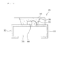
- FIG. 11 is a sectional view illustrating a light emitting device package according to an exemplary embodiment.
- the light emitting device package according to the illustrated embodiment which is designated by reference numeral "300" includes a body 310, first and second lead frames 321 and 322 mounted on the body 310, the light emitting device 100 according to one the above-described embodiment, which is mounted on the body 300, to be electrically connected to the first and second lead frames 321 and 322, and a mold 340 encompassing the light emitting device 100.
- the body 310 may be made of a silicon material, a synthetic resin material, or a metal material.
- a conductive material such as a metal material
- an insulating layer is coated over the surface of the body 310, although not shown, in order to avoid electrical short circuit between the first and second lead frames 321 and 322.
- the first and second lead frames 321 and 322 are electrically isolated from each other, and supply current to the light emitting device 100.
- the first and second lead frames 321 and 322 may also reflect light generated from the light emitting device 100 so as to achieve an enhancement in luminous efficacy.
- the first and second lead frames 321 and 322 may function to outwardly dissipate heat generated from the light emitting device 100.
- the light emitting device 100 may be mounted on the body 310 or on the first lead frame 321 or second lead frame 322. In the illustrated embodiment, the light emitting device 100 is directly electrically connected to the first lead frame 321 while being connected to the second lead frame 322 via a wire 330. The light emitting device 100 may be connected to the lead frames 321 and 322, using a flip-chip method or a die-bonding method, in place of the wire-bonding method.
- the mold 340 encapsulates the light emitting device 100, to protect the light emitting device 100.
- the mold 340 includes phosphors 350, to change the wavelength of light emitted from the light emitting device 100.
- the phosphors 350 may include garnet-based phosphors, silicate-based phosphors, nitride-based phosphors, or oxynitride-based phosphors.
- the garnet-based phosphors may be YAG (Y 3 Al 5 O 12 :Ce 3+ ) or TAG (Tb 3 Al 5 O 12 :Ce 3+ ) .
- the silicate-based phosphors may be (Sr,Ba,Mg,Ca) 2 SiO 4 :Eu2 + .
- the nitride-based phosphors may be CaAlSiN 3 :Eu 2+ containing SiN.
- the oxynitride-based phosphors may be Si 6-x Al x O x N s-x :Eu 2+ (0 ⁇ X ⁇ 6).
- Light of a first wavelength range emitted from the light emitting device 100 is excited by the phosphors 350, so that it is changed into light of a second wavelength range.
- the optical path thereof may be changed.
- a plurality of light emitting device packages each of which has the above-described structure according to the illustrated embodiment, is prepared, and is then arrayed on a substrate.
- Optical members namely, light guide plates, prism sheets, diffusion sheets, etc., may be arranged on optical paths of the light emitting device packages.
- Such light emitting device packages, substrate, and optical members may function as a light unit.
- a display apparatus, an indication apparatus or a lighting system may be implemented using the semiconductor light emitting devices or light emitting device packages described in conjunction with the above-described embodiments.
- the lighting system may include, for example, a lamp or a street lamp.
- FIG. 12 is an exploded perspective view illustrating a lighting apparatus according to an exemplary embodiment, in which light emitting device packages according to the above-described embodiment are disposed.
- the lighting apparatus includes a light source 600 for projecting light, a housing 400 in which the light source 600 is mounted, a heat dissipation unit 500 for dissipating heat generated from the light source 600, and a holder 700 for coupling the light source 600 and heat dissipation unit 500 to the housing 400.
- the housing 400 includes a socket connection part 410 connected to an electric socket (not shown), and a body part 420 connected to the socket connection part 410.
- the light source 600 is received in the body part 420.
- a plurality of air holes 430 may be formed through the body part 420.
- a single air hole 430 may be formed through the body part 420.
- the plural air holes 430 are circumferentially arranged, various arrangements thereof may be possible.
- the light source 600 includes a circuit board 610 and a plurality of light emitting device packages 650 mounted on the circuit board 610.
- the light emitting device packages 650 may have a structure described with reference to FIG. 11 .
- the holder 700 is disposed under the light source 600.
- the holder 700 includes a frame and air holes.
- an optical member may be disposed under the light source 600 so as to diffuse, scatter or converge light projected from the light emitting device packages 650 of the light source 600.
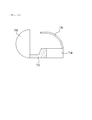
- FIG. 13 is a view illustrating a head lamp according to an exemplary embodiment, in which a light emitting device package according to the above-described embodiment is disposed.
- light emitted from a light emitting module 710 passes through a lens 740 after being reflected by a reflector 720 and a shade 730, so as to be directed forwardly of a vehicle body.
- a plurality of light emitting devices may be mounted in the light emitting device package included in the light emitting module 710, although the present disclosure is not limited thereto.
- the light emitting device package which includes the light emitting device according to one of the above-described embodiments, has an enhanced light extraction efficiency in accordance with the thickness reduction of the first-conductivity-type semiconductor layer, the luminous efficacy of the light emitting module 710 may be enhanced.
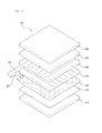
- FIG. 14 is a view illustrating a display apparatus according to an exemplary embodiment in which light emitting device packages according to the above-described embodiment are disposed.
- the display apparatus As shown in FIG. 14 , the display apparatus according to the illustrated embodiment, which is designated by reference numeral "800", includes a light source module, a reflection plate 820 disposed on a bottom cover 810, a light guide plate 840 disposed in front of the reflection plate 820 to guide light emitted from the light source module to a front side of the display apparatus 800, first and second prism sheets 850 and 860 disposed in front of the light guide plate 840, a panel 870 disposed in front of the second prism sheet 860, and a color filter 880 disposed in front of the panel 870.
- a light source module As shown in FIG. 14 , the display apparatus according to the illustrated embodiment, which is designated by reference numeral "800", includes a light source module, a reflection plate 820 disposed on a bottom cover 810, a light guide plate 840 disposed in front of the reflection plate 820 to guide light emitted from the light source module to a front side of the display apparatus 800, first and second prism sheets 850
- the light source module includes a circuit board 830 and light emitting device packages 835 mounted on the circuit board 830.
- a printed circuit board PCB
- the light emitting device packages 835 may have the configuration described above in conjunction with FIG. 11 .
- the bottom cover 810 serves to receive the constituent elements of the display apparatus 800.
- the reflection plate 820 may be provided as a separate element, as shown in FIG. 14 , or may be formed as a material having high reflectivity is coated over a rear surface of the light guide plate 840 or a front surface of the bottom cover 810.
- the reflection plate 820 may be made of a material having high reflectivity and capable of being formed into an ultra thin structure.
- Polyethylene terephthalate (PET) may be used for the reflection plate 820.
- the light guide plate 840 serves to scatter light emitted from the light source module so as to uniformly distribute the light throughout all regions of a liquid crystal display apparatus. Therefore, the light guide plate 840 may be made of a material having high refractivity and transmissivity.
- the material of the light guide plate 840 may include polymethylmethacrylate (PMMA), polycarbonate (PC) or polyethylene (PE).
- PMMA polymethylmethacrylate
- PC polycarbonate
- PE polyethylene
- the light guide plate may be dispensed with. In this case, an air guide system, which transfers light in a space over the reflective sheet 820, may be implemented.
- the first prism sheet 850 may be formed by coating a polymer exhibiting light transmittance and elasticity over one surface of a base film.
- the first prism sheet 850 may have a prism layer having a plurality of three-dimensional structures in the form of a repeated pattern.
- the pattern may be of a stripe type in which ridges and valleys are repeated.
- the second prism sheet 860 may have a similar structure to the first prism sheet 850.
- the second prism sheet 860 may be configured such that the orientation direction of ridges and valleys formed on one surface of the base film of the second prism sheet 860 is perpendicular to the orientation direction of the ridges and valleys formed on one surface of the base film of the first prism sheet 850.
- Such a configuration serves to uniformly distribute light transmitted from the light module and the reflective sheet 820 toward the entire surface of the panel 870.
- an optical sheet may be constituted by the first prism sheet 850 and second prism sheet 860.
- the optical sheet may include other combinations, for example, a microlens array, a combination of a diffusion sheet and a microlens array, and a combination of a prism sheet and a microlens array.
- a liquid crystal display panel may be used as the panel 870. Further, instead of the liquid crystal display panel 870, other kinds of display devices requiring light sources may be provided.
- the display panel 870 is configured such that a liquid crystal layer is located between glass bodies (transparent substrates), and polarizing plates are mounted on both glass bodies so as to utilize polarizing properties of light.
- the liquid crystal layer has properties between a liquid and a solid. That is, in the liquid crystal layer, liquid crystals which are organic molecules having fluidity like the liquid are regularly oriented, and the liquid crystal layer displays an image using change of such molecular orientation due to an external electric field.
- the liquid crystal display panel used in the display apparatus is of an active matrix type, and uses transistors as switches to adjust voltage applied to each pixel.
- the color filter 880 is provided on the front surface of the panel 870, and transmits only a red, green or blue light component of light projected from the panel 870 per pixel, thereby displaying an image.
- the semiconductor layer thereof has a reduced thickness. Accordingly, the light extraction efficiency of the light emitting device may be enhanced because the length of a path, along which light generated from an active layer travels before being outwardly emitted, is reduced.
Landscapes
- Led Devices (AREA)
- Non-Portable Lighting Devices Or Systems Thereof (AREA)
Abstract
Description
- This application claims priority to Korean Patent Application No.
10-2011-0102836 - Embodiments relate to a light emitting device, a light emitting device package and a lighting apparatus including the same.
- Light emitting devices, such as light emitting diodes (LEDs) and laser diodes (LDs), which use a Group III-V or Group II-VI compound semiconductor material, may render various colors such as red, green, blue, and ultraviolet by virtue of development of thin film growth technologies and device materials. It may also be possible to produce white light at high efficiency using fluorescent materials or through color mixing. Further, the light emitting devices have advantages, such as low power consumption, semi-permanent lifespan, fast response time, safety, and environmental friendliness as compared to conventional light sources, such as fluorescent lamps and incandescent lamps.
- Therefore, these light emitting elements are increasingly applied to transmission modules of optical communication units, light emitting diode backlights as a replacement for cold cathode fluorescent lamps (CCFLs) constituting backlights of liquid crystal display (LCD) devices, and lighting apparatuses using white light emitting diodes as a replacement for fluorescent lamps or incandescent lamps, headlights for vehicles and traffic lights.
- In the case of a light emitting device having a via hole, the thickness thereof is greater than that of a light emitting device having a semiconductor layer with a general thickness. For this reason, the length of a path, along which light generated from an active layer travels before being outwardly emitted, is long, so that the amount of light absorbed in the semiconductor layer disposed over the active layer increases. As a result, the light extraction efficiency of the light emitting device may be degraded.
- Embodiments achieve an enhancement in the light extraction efficiency of a light emitting device through a reduction in the thickness of a semiconductor layer included in the light emitting device.
- In one embodiment, a light emitting device includes a light emitting structure including a first-conductivity-type semiconductor layer, an active layer, and a second-conductivity-type semiconductor layer, a second electrode layer disposed beneath the light emitting structure and electrically connected to the second-conductivity-type semiconductor layer, a first electrode layer including a main electrode disposed beneath the second electrode layer, and at least one contact electrode branching from the main electrode and extending through the second electrode layer, the second-conductivity-type semiconductor layer and the active layer, to contact the first-conductivity-type semiconductor layer, and an insulating layer interposed between the first electrode layer and the second electrode layer and between the first electrode layer and the light emitting structure, wherein the first-conductivity-type semiconductor layer includes a first region and a second region having a smaller height than the first region, and the first region overlaps with the contact electrode.
- In another embodiment, a light emitting device includes a light emitting structure including a first-conductivity-type semiconductor layer, an active layer, and a second-conductivity-type semiconductor layer, which are stacked in a predetermined direction, a second electrode layer disposed beneath the light emitting structure and electrically connected to the second-conductivity-type semiconductor layer, a first electrode layer including a main electrode disposed beneath the second electrode layer, and at least one contact electrode branching from the main electrode and extending through the second electrode layer, the second-conductivity-type semiconductor layer and the active layer, to contact the first-conductivity-type semiconductor layer, and an insulating layer interposed between the first electrode layer and the second electrode layer and between the first electrode layer and the light emitting structure, wherein the first-conductivity-type semiconductor layer includes a first region and a second region having a smaller thickness than the first region, and the first region overlaps with the contact electrode in the predetermined direction.
- The first region may have a width equal to or greater than a width of the contact electrode.
- The width of the first region may correspond to 1 to 5 times the width of the contact electrode.
- A roughness or a pattern may be formed at an upper surface of the first-conductivity-type semiconductor layer.
- The light emitting device may further include a passivation layer formed on side surfaces of the light emitting structure, to cover at least a portion of the second-conductivity-type semiconductor layer, at least a portion of the active layer, and at least a portion of the first-conductivity-type semiconductor layer. A roughness may be formed at a portion of the contact electrode contacting the first-conductivity-type semiconductor layer.
- A portion of the second electrode layer may be exposed outside the light emitting structure, and an electrode pad may be formed on the exposed portion of the second electrode layer.
- The second electrode layer may include an ohmic layer and/or a reflective layer disposed beneath the second-conductivity-type semiconductor layer.
- The second electrode layer may include a current spreading layer, and the electrode pad may be disposed to contact the current spreading layer.
- The light emitting device may further include a passivation layer formed on side surfaces of the first region.
- The first region may have at least one of a stripe shape, a circular prism shape, a conical shape, a pyramid shape, a square prism shape, and a hemi-spherical shape.
- In another embodiment, a light emitting device package comprises a body; first and second lead frames mounted on the body; and a light emitting device which is mounted on the body and electrically connected to the first and second lead frames, wherein the light emitting device comprises a light emitting structure comprising a first-conductivity-type semiconductor layer, an active layer, and a second-conductivity-type semiconductor layer, which are stacked in a predetermined direction; a second electrode layer disposed beneath the light emitting structure and electrically connected to the second-conductivity-type semiconductor layer; a first electrode layer comprising a main electrode disposed beneath the second electrode layer, and at least one contact electrode branching from the main electrode and extending through the second electrode layer, the second-conductivity-type semiconductor layer and the active layer, to contact the first-conductivity-type semiconductor layer; and an insulating layer interposed between the first electrode layer and the second electrode layer and between the first electrode layer and the light emitting structure, and wherein the first-conductivity-type semiconductor layer comprises a first region and a second region having a smaller thickness than the first region, and the first region overlaps with the contact electrode in the predetermined direction.
- In another embodiment, a lighting apparatus includes a light source for emitting light, the light source including a plurality of light emitting device packages mounted on a circuit board, a housing, in which the light source is mounted, a heat dissipation unit to dissipate heat generated from the light source, and a holder for coupling the light source and the heat dissipation unit to the housing, wherein each of the light emitting device packages includes a body, first and second lead frames disposed on the body, and a light emitting device disposed on the body and electrically connected to the first and second lead frames, wherein the light emitting device includes a light emitting structure including a first-conductivity-type semiconductor layer, an active layer, and a second-conductivity-type semiconductor layer, which are stacked in a predetermined direction, a second electrode layer disposed beneath the light emitting structure and electrically connected to the second-conductivity-type semiconductor layer, a first electrode layer including a main electrode disposed beneath the second electrode layer, and at least one contact electrode branching from the main electrode and extending through the second electrode layer, the second-conductivity-type semiconductor layer and the active layer, to contact the first-conductivity-type semiconductor layer, and an insulating layer interposed between the first electrode layer and the second electrode layer and between the first electrode layer and the light emitting structure, and wherein the first-conductivity-type semiconductor layer includes a first region and a second region having a smaller thickness than the first region, and the first region overlaps with the contact electrode in the predetermined direction.
- Arrangements and embodiments may be described in detail with reference to the following drawings in which like reference numerals refer to like elements and wherein:
-
FIG. 1A is a sectional view illustrating a light emitting device according to an exemplary embodiment; -
FIGs. 1B to 1G are perspective views illustrating light emitting devices according to various embodiments, respectively; -
FIGS. 2 to 10 are views illustrating a light emitting device manufacturing method according to an exemplary embodiment; -
FIG. 11 is a sectional view illustrating a light emitting device package according to an exemplary embodiment; -
FIG. 12 is an exploded perspective view illustrating a lighting apparatus according to an exemplary embodiment, in which light emitting device packages according to the above-described embodiment are disposed; -
FIG. 13 is a view illustrating a head lamp according to an exemplary embodiment, in which a light emitting device package according to the above-described embodiment is disposed; and -
FIG. 14 is a view illustrating a display apparatus according to an exemplary embodiment in which light emitting device packages according to the above-described embodiment are disposed. - Hereinafter, embodiments will be described with reference to the annexed drawings.
- It will be understood that when an element is referred to as being "on" or "under" another element, it can be directly on/under the element, and one or more intervening elements may also be present. When an element is referred to as being "on" or "under", "under the element" as well as "on the element" can be included based on the element.
- In the drawings, the thickness or size of each layer is exaggerated, omitted, or schematically illustrated for convenience of description and clarity. Also, the size or area of each constituent element does not entirely reflect the actual size thereof.
-
FIG. 1A is a sectional view illustrating a light emitting device according to an exemplary embodiment.FIGs. 1B to 1G are perspective views illustrating light emitting devices according to various embodiments, respectively. - The light emitting device according to each of the illustrated embodiments, which is designated by
reference numeral 100, includes asupport substrate 110, afirst electrode layer 120 disposed over thesupport substrate 110, asecond electrode layer 130 disposed over thefirst electrode layer 120, and alight emitting structure 140 disposed over thesecond electrode layer 130. Thelight emitting structure 140 includes a first-conductivity-type semiconductor layer 146, anactive layer 144, and a second-conductivity-type semiconductor layer 142, which are stacked in a same direction. - The
light emitting device 100 may include a light emitting diode (LED) using a plurality of compound semiconductor layers, for example, semiconductor layers made of Group III-V elements. The LED may be a colored LED to emit blue, green, or red light, or an ultraviolet (UV) LED, although the present disclosure is not limited thereto. Emission of light from the LED may be achieved using various semiconductors, although the present disclosure is not limited thereto. - The
light emitting structure 140 may be formed using, for example, metal organic chemical vapor deposition (MOCVD), chemical vapor deposition (CVD), plasma-enhanced chemical vapor deposition (PECVD), molecular beam epitaxy (MBE), hydride vapor phase epitaxy (HVPE), or the like. Of course, the formation method is not limited to the above-described methods. - The first-conductivity-
type semiconductor layer 146 may be made of a semiconductor compound, for example, a Group III-V or Group II-VI compound semiconductor. The first-conductivity-type semiconductor layer 146 may be doped with a first-conductivity-type dopant. When the first-conductivity-type semiconductor layer 146 is an n-type semiconductor layer, the first-conductivity-type dopant is an n-type dopant. The n-type dopant may include Si, Ge, Sn, Se, or Te, although the present disclosure is not limited thereto. When the first-conductivity-type semiconductor layer 146 is a p-type semiconductor layer, the first-conductivity-type dopant is a p-type dopant. The p-type dopant may include Mg, Zn, Ca, Sr, Ba, or the like, although the present disclosure is not limited thereto. - The first-conductivity-
type semiconductor layer 146 may include a semiconductor material having a formula of AlxInyGa1-x-yN (0 ≤ x ≤ 1, 0 ≤ y ≤ 1, and 0 ≤ x+y ≤ 1). For example, the first-conductivity-type semiconductor layer 146 may be made of at least one of GaN, InN, AlN, InGaN, AlGaN, InAlGaN, AlInN, AlGaAs, InGaAs, AlInGaAs, GaP, AlGaP, InGaP, AlInGaP, and InP. - In order to achieve an enhancement in light extraction efficiency, a roughness or
pattern 160 may be formed on an upper surface of the first-conductivity-type semiconductor layer 146. - In the
active layer 144, electrons and holes meet, thereby emitting light with energy determined by the intrinsic energy band of the material of the active layer 144 (light emitting layer). - The
active layer 144 may have at least one of a single quantum well structure, a multi quantum well structure, a quantum wire structure, and a quantum dot structure. For example, theactive layer 144 may have a multi quantum well structure through injection of tri-methyl gallium gas (TMGa), ammonia gas (NH3), nitrogen gas (N2), and tri-methyl indium gas (TMIn), although the present disclosure is not limited thereto. - The
active layer 144 may have well and barrier layers having a layer pair structure made of at least one of InGaN/GaN, InGaN/InGaN, GaN/AlGaN, InAlGaN/GaN, GaAs(InGaAs)/AlGaAs, and GaP(InGaP)/AlGaP, although the present disclosure is not limited thereto. The well layer may be made of a material having a narrower band gap than the barrier layer. - A conductive clad layer (not shown) may be formed over and/or beneath the
active layer 144. The conductive clad layer may be made of a semiconductor having a wider bandgap than the barrier layer of theactive layer 144. For example, the conductive clad layer may be made of GaN, AlGaN or InAlGaN, or may have a super-lattice structure. The conductive clad layer may be doped with a dopant to have an n-type or p-type conductivity. - The second-conductivity-
type semiconductor layer 142 may be made of a semiconductor compound, for example, a Group III-V compound semiconductor doped with a second-conductivity-type dopant. For example, the second-conductivity-type semiconductor layer 142 may include a semiconductor material having a formula of InxAlyGa1-x-yN (0 ≤ x ≤ 1, 0 ≤ y ≤ 1, 0 ≤ x + y ≤ 1). When the second-conductivity-type semiconductor layer 142 is a p-type semiconductor layer, the second-conductivity-type dopant is a p-type dopant. The p-type dopant may include Mg, Zn, Ca, Sr, Ba, or the like, although the present disclosure is not limited thereto. When the second-conductivity-type semiconductor layer 142 is an n-type semiconductor layer, the second-conductivity-type dopant is an n-type dopant. The n-type dopant may include Si, Ge, Sn, Se, or Te, although the present disclosure is not limited thereto. - In the illustrated embodiments, the
first semiconductor layer 146 may be implemented as an n-type semiconductor layer, and thesecond semiconductor layer 142 may be implemented as a p-type semiconductor layer. Alternatively, thefirst semiconductor layer 146 may be implemented as a p-type semiconductor layer, and thesecond semiconductor layer 142 may be implemented as an n-type semiconductor layer. Over the second-conduction-type semiconductor layer 142, a semiconductor layer having an opposite polarity to the second conduction type may be formed. For example, when the second-conduction-type semiconductor layer 142 is a p-type semiconductor layer, an n-type semiconductor layer (not shown) may be formed over the second-conduction-type semiconductor layer 142. Thus, thelight emitting structure 140 may be implemented as one of an n-p junction structure, a p-n junction structure, an n-p-n junction structure, and a p-n-p junction structure. - The
support substrate 110 supports thelight emitting structure 140. Thesupport substrate 110 may be a conductive substrate or an insulating substrate. Also, thesupport substrate 110 may be made of a material having high electrical conductivity and high thermal conductivity. For example, thesupport substrate 110 may be formed as a base substrate having a certain thickness, using a material selected from the group consisting of molybdenum (Mo), silicon (Si), tungsten (W), copper (Cu), aluminum (Al), and alloys thereof. Also, thesupport substrate 110 may selectively include gold (Au), a Cu alloy, Ni, Cu-W, a carrier wafer (for example, GaN, Si, Ge, GaAs, ZnO, SiGe, SiC, SiGe, Ga2O3, or the like), a conductive sheet, or the like. - The
first electrode layer 120 is formed over thesupport substrate 110. Thefirst electrode layer 120 may be made of a metal. Thefirst electrode layer 120 may include at least one of an ohmic layer, a reflective layer, and a bonding layer. Thefirst electrode layer 120 may come into ohmic contact with afirst semiconductor layer 146, which will be described later, using a reflective metal or a conductive oxide. - The
first electrode layer 120 may be made of Ag, Ni, Al, Rh, Pd, Ir, Ru, Mg, Zn, Pt, Au, Hf, or a selective combination thereof. Thefirst electrode layer 120 may be formed to have a single layer structure or a multilayer structure, using a reflective electrode material having ohmic characteristics. When thefirst electrode layer 120 performs an ohmic function, the ohmic layer may be dispensed with. - The
first electrode layer 120 may be made of at least one of indium tin oxide (ITO), indium zinc oxide (IZO), indium zinc tin oxide (IZTO), indium aluminum zinc oxide (IAZO), indium gallium zinc oxide (IGZO), indium gallium tin oxide (IGTO), aluminum zinc oxide (AZO), antimony tin oxide (ATO), gallium zinc oxide (GZO), IrOx, RuOx, NiO, RuOx/ITO, Ni/IrOx/Au, and Ni/IrOx/Au/ITO, although the present disclosure is not limited thereto. - The
first electrode layer 120 may include a bonding layer. In this case, the bonding layer may include a barrier metal or a bonding metal. For example, the bonding layer may include at least one of Ti, Au, Sn, Ni, Cr, Ga, In, Bi, Cu, Ag, and Ta. - When the
first electrode layer 120 does not include a bonding layer, aseparate bonding layer 115 may be formed to achieve bonding to thesupport substrate 110, as shown inFIG. 1 . Thebonding layer 115 may be made of a material selected from the group consisting of Au, Sn, In, Ag, Ni, Nb, Cu, and alloys thereof, although the present disclosure is not limited thereto. - The
second electrode layer 130 is formed on amain electrode 120a of thefirst electrode layer 120, which will be described later. An insulatinglayer 170 is disposed between thesecond electrode 130 and thefirst electrode layer 120, to electrically insulate the first and second electrode layers 120 and 130. - The
second electrode layer 130 may have a structure of ohmic layer/reflective layer/bonding layer, a structure of ohmic layer/reflective layer, or a structure of reflective layer (including ohmic characteristics)/bonding layer, although the present disclosure is not limited thereto. Also, thesecond electrode layer 130 may include a current spreading layer. For example, thesecond electrode layer 130 may have a structure in which a current spreadinglayer 136, areflective layer 134, and anohmic layer 132 are sequentially stacked over the insulatinglayer 170. - The current spreading
layer 136 may be made of a metal having high electrical conductivity. The current spreadinglayer 136 is electrically connected to anelectrode pad 190, which will be described later, to supply current to the second-conductivity-type semiconductor layer 142. The current spreadinglayer 136 may be made of, for example, at least one selected from the group consisting of Ti, Au, Ni, In, Co, W, and Fe, although the present disclosure is not limited thereto. - The
reflective layer 134 is disposed over the current spreadinglayer 136. Thereflective layer 134 may be made of a reflection material having reflectance of 50% or more. Thereflective layer 134 may be made of, for example, a selective combination of Ag, Ni, Al, Rh, Pd, Ir, Ru, Mg, Zn, Pt, Au, and Hf. Alternatively, thereflective layer 134 may be formed to have a multilayer structure, using the metal materials and a light-transmitting conductive material such as IZO, IZTO, IAZO, IGZO, IGTO, AZO, and ATO. Thereflective layer 134 may have a lamination structure of IZO/Ni, AZO/Ag, IZO/Ag/Ni, AZO/Ag/Ni, or the like. When thereflective layer 134 is made of a material coming into ohmic contact with the light emitting structure 140 (for example, the second-conductivity-type semiconductor layer 142), theohmic layer 132 may be dispensed with, although the present disclosure is not limited thereto. - The
ohmic layer 132 may be disposed to contact the second-conductivity-type semiconductor layer 142. When the second-conductivity-type semiconductor layer 142 is a p-type semiconductor layer, the second-conductivity-type semiconductor layer 142 has high contact resistance due to a low dopant concentration thereof. For this reason, the second-conductivity-type semiconductor layer 142 may exhibit poor metal ohmic characteristics. Theohmic layer 132 is adapted to improve the ohmic characteristics. Theohmic layer 132 is not a necessity. - Since the
ohmic layer 132 is interposed between thelight emitting structure 140 and thereflective layer 134, it may be formed using a transparent electrode or the like. Also, theohmic layer 132 may have a multilayer structure or a plurality of patterns. - The
ohmic layer 132 may have a thickness of about 200Å. For theohmic layer 132, a light-transmitting conductive layer or a metal may be selectively used. For example, theohmic layer 132 may be made of at least one of indium tin oxide (ITO), indium zinc oxide (IZO), indium zinc tin oxide (IZTO), indium aluminum zinc oxide (IAZO), indium gallium zinc oxide (IGZO), indium gallium tin oxide (IGTO), aluminum zinc oxide (AZO), antimony tin oxide (ATO), gallium zinc oxide (GZO), IZO nitride (IZON), Al-GaZnO (AGZO), In-GaZnO (IGZO), ZnO, IrOx, RuOx, NiO, RuOx/ITO, Ni/IrOx/Au, Ni/IrOx/Au/ITO, Ag, Ni, Cr, Ti, Al, Rh, Pd, Ir, Sn, In, Ru, Mg, Zn, Pt, Au, and Hf, although the present disclosure is not limited thereto. - The
first electrode layer 120 includes themain electrode 120a, and at least onecontact electrode 120b, which branches from themain electrode 120a, and contacts the first-conductivity-type semiconductor layer 146 after extending through thesecond electrode layer 130, second-conductivity-type semiconductor layer 142, andactive layer 144. - A plurality of
contact layers 120b may branch from themain electrode 120a of thefirst electrode layer 120 while being spaced apart from one another. When thefirst electrode layer 120 includes a plurality ofcontact electrodes 120b, it may be possible to smoothly supply current to the first-conductivity-type semiconductor layer 146. Thecontact electrodes 120b may have at least one of patterns having various shapes when viewed from the top side, that is, a radial pattern, a cross pattern, a line pattern, a curve pattern, a loop pattern, a link pattern, and a ring pattern, although the present disclosure is not limited thereto. - Meanwhile, an ohmic layer may be formed on the
contact layer 120b, to allow thecontact electrode 120b to come into ohmic contact with the first-conductivity-type semiconductor layer 146. - A
roughness 122 may be formed at a portion of thecontact electrode 120b contacting the first-conductivity-type semiconductor layer 146. Theroughness 122 is a random pattern of irregularities formed at a portion of thecontact electrode 120b contacting the first-conductivity-type semiconductor layer 146. Theroughness 122 may be formed using a wet etching process or a dry etching process. - The
roughness 122 increase the contact area between thefirst electrode layer 120 and the first-conductivity-type semiconductor layer 146. As the contact area between thefirst electrode layer 120 and the first-conductivity-type semiconductor layer 146 increases, the electrode contact area is increased, thereby achieving an improvement in the electrical characteristics of thelight emitting device 100. In addition, the bonding force between thefirst electrode layer 120 and the first-conductivity-type semiconductor layer 146 is increased, thereby achieving an enhancement in the reliability of thelight emitting device 100. - The insulating layer is formed between the
first electrode layer 120 and thesecond electrode layer 130 and on the side walls of thefirst electrode layer 120 andcontact electrode 120b, to insulate thefirst electrode layer 120 from other layers, for example, thelayers - The insulating
layer 170 may be made of a nonconductive oxide or nitride. For example, the insulatinglayer 170 may be comprised of at least one of a silicon oxide (SiO2) layer, an oxide nitride layer, and an aluminum oxide layer. - A portion of the
second electrode layer 130, for example, a portion of the current spreadinglayer 136 of thesecond electrode layer 130 in the embodiment ofFIG. 1 , may be exposed outside thelight emitting structure 140. Theelectrode pad 190 may be formed on the exposed portion of thesecond electrode layer 130. - The
electrode pad 190 may be made of at least one of aluminum (Al), titanium (Ti), chromium (Cr), nickel (Ni), copper (Cu), and gold (Au), to have a single layer structure or a multilayer structure. - A
passivation layer 180 may be formed on side surfaces of thelight emitting structure 140. For example, thepassivation layer 180 may be disposed to cover portions of the second-conductivity-type semiconductor layer 142,active layer 144, and first-conductivity-type semiconductor layer 146. - Another
passivation layer 181 may be formed on side surfaces ofconvex portions 148a of a concave/convex structure 148 included in the first-conductivity-type semiconductor layer 146, which will be described later. - The
passivation layer 180 is made of an insulating material, to avoid electrical short circuit between thelight emitting structure 140 and theelectrode pad 190. Thepassivation layer 180 may be made of the same material as the insulatinglayer 170. - The concave/
convex structure 148 of the first-conductivity-type semiconductor layer 146 includes, in addition to theconvex portions 148a, aconcave portion 148b having a lower height than theconvex portions 148a. Theconvex portions 148a may overlap with thecontact electrodes 120b of thefirst electrode layer 120. - That is, the
convex portions 148a may overlap with thecontact electrodes 120b of thefirst electrode layer 120 in a lamination direction of thelight emitting structure 140. - Referring to
FIGS. 1B to 1G , the convex portions 140a may have at least one of a stripe shape, a square prism shape, a circular prism shape, a conical shape, a pyramid shape, and a hemi-spherical shape, although the present disclosure is not limited thereto. - Although a roughness or
pattern 160 is formed on the first-conductivity-type semiconductor layer 146, it is not shown inFIGS. 1B to 1G , for convenience of illustration. - Conventional light emitting devices are thick because the first-conductivity-type semiconductor layer thereof is thickly formed to secure a region corresponding to the height of the contact electrode of the first electrode layer.
- If the first-conductivity-
type semiconductor layer 146, which is an upper layer of thelight emitting structure 140, is thick, the length of the path, along which light generated from theactive layer 144 travels before being outwardly emitted, is long, so that a part of the light may be absorbed in the first-conductivity-type semiconductor layer 146. As a result, the light extraction efficiency of the light emitting device may be degraded. - In the illustrated embodiments, the first-conductivity-
type semiconductor layer 146 has the concave/convex structure 148. Eachconvex portion 148a of the concave/convex structure 148 has a predetermined height difference H2 from the upper surface of thecorresponding contact electrode 120b, to secure reliability of the light emitting device. At a portion of the first-conductivity-type semiconductor layer 146 where thecontact electrodes 120b are not present, theconcave portion 148b of the concave/convex structure 148 is formed to reduce the height of the first-conductivity-type semiconductor layer 146 to a height H3. Thus, the light extraction efficiency of thelight emitting device 100 may be enhanced. - That is, the
concave portion 148b has a smaller thickness than theconvex portions 148a. - The predetermined height difference H2 should be kept between the upper surface of the first-conductivity-
type semiconductor layer 146 and the upper surface of eachcontact electrode 120b. If thecontact electrode 120b is too close to the upper surface of the first-conductivity-type semiconductor layer 146, a portion of thecontact electrode 120b may be outwardly exposed in a texturing process to form a roughness or pattern on the surface of the first-conductivity-type semiconductor layer 146, so that electrical short circuit may occur. The height difference H2 may be 1 to 5µm, to avoid interference with light extraction while securing reliability of the light emitting device. - Also, the height difference H3 between the
concave portion 148b of the concave/convex structure 148 in the first-conductivity-type semiconductor layer 146 and theactive layer 144 of thelight emitting structure 140 should be kept at a predetermined degree. If theactive layer 142 is too close to the upper surface of the first-conductivity-type semiconductor layer 146, a portion of theactive layer 144 may be outwardly exposed in the texturing process to form a roughness or pattern on the surface of the first-conductivity-type semiconductor layer 146, so that reliability of the light emitting device may be degraded. The height difference H3 may be 0.5 to 4µm, to avoid interference with light extraction while securing reliability of the light emitting device. - The total height H1 of the
light emitting structure 140 may be 1 to 5µm. - Each
convex portion 148a of the concave/convex structure 148 may vertically overlap with thecorresponding contact electrode 120b of thefirst electrode layer 120. Theconvex portion 148 may also have a width W2 equal to or greater than a width W1 of thecontact electrode 120b. - The width W2 of each
convex portion 148a may depend on the width of the spacing between thecontact electrodes 120b branching from themain electrode 120a of thefirst electrode layer 120. In an exemplary embodiment, the width W3 of theconvex portions 148a may be 1 to 5 times the width W1 of thecontact electrodes 120b. - In accordance with the illustrated embodiments, it may be possible to secure reliability of the light emitting device because each
convex portion 148a of the first-conductivity-type semiconductor layer 146 maintains the predetermined height difference H2 from thecorresponding contact electrode 120b while vertically overlapping with thecontact electrode 120b. Also, it may be possible to enhance the light extraction efficiency of the light emitting device because theconcave portion 148b is formed at the portion of the first-conductivity-type semiconductor layer 146 where thecontact electrodes 120b are not disposed, to reduce the thickness of the first-conductivity-type semiconductor layer 146. - The concave/
convex structure 148 of the first-conductivity-type semiconductor layer 146 may be formed by forming a photoresist (PR) layer over the upper surface of the first-conductivity-type semiconductor layer 146, covering a mask with a pattern on the PR layer, and irradiating ultraviolet (UV) light to the resulting structure. - For the PR layer, a positive PR film, in which a light-irradiated portion thereof is etched during development, or a negative PR film, in which a light-irradiated portion thereof is left after development, may be used.
- Since light generated from the
active layer 144 is emitted not only from the upper surface of the first-conductivity-type semiconductor layer 146, but also from the side surfaces of theconvex portions 148a, the concave/convex structure 148 formed at the first-conductivity-type semiconductor layer 146 increases the light emission area. Thus, the luminous characteristics of the light emitting device may be improved. -
FIGS. 2 to 10 are views illustrating a light emitting device manufacturing method according to an exemplary embodiment. Hereinafter, the light emitting device manufacturing method will be described with reference toFIGs. 2 to 10 . - Referring to
FIG. 2 , thelight emitting structure 140 is grown over asubstrate 101. - The
substrate 101 may be formed using a material suitable for growth of a semiconductor material or a carrier wafer. Thesubstrate 101 may also be made of a material having excellent thermal conductivity. Thesubstrate 101 may be a conductive substrate or an insulating substrate. For example, thesubstrate 101 may be made of at least one of sapphire (Al2O3), SiC, GaAs, GaN, ZnO, Si, GaP, InP, Ge, and Ga2O3. An irregularity structure may be formed on thesubstrate 101, although the present disclosure is not limited thereto. Wet washing may be performed upon thesubstrate 101, to remove impurities from the surface of thesubstrate 101. - The
light emitting structure 140 may be formed by sequentially forming, over thesubstrate 101, the first-conductivity-type semiconductor layer 146,active layer 144, and second-conductivity-type semiconductor layer 142. - The
light emitting structure 140 may be formed using, for example, metal organic chemical vapor deposition (MOCVD), chemical vapor deposition (CVD), plasma-enhanced chemical vapor deposition (PECVD), molecular beam epitaxy (MBE), hydride vapor phase epitaxy (HVPE), or the like. Of course, the formation method is not limited to the above-described methods. - The first-conductivity-
type semiconductor layer 146 is grown to a thickness D1, which is greater than the thickness of the first-conductivity-type semiconductor layer formed in a general light emitting device having no contact electrode. - A buffer layer (not shown) may be grown between the
light emitting structure 140 and thesubstrate 101. The buffer layer is adapted to reduce lattice mismatch and coefficient of thermal expansion differences between the material of thesubstrate 101 and the material of the layer formed over thesubstrate 101. The buffer layer may be made of a Group III-V compound semiconductor, for example, at least one of GaN, InN, AIN, InGaN, AlGaN, InAlGaN, and AlInN. An undoped semiconductor layer may be formed over the buffer layer, although the present disclosure is not limited thereto. - Referring to
FIG. 3 , thesecond electrode layer 130 is then formed on the second-conductivity-type semiconductor layer 142. Thesecond electrode layer 130 may have a structure of ohmic layer/reflective layer/bonding layer, a structure of ohmic layer/reflective layer, or a structure of reflective layer/bonding layer. Also, thesecond electrode layer 130 may include a current spreading layer. - For example, the
ohmic layer 132 andreflective layer 134 may be formed on the second-conductivity-type semiconductor layer 142, and the current spreadinglayer 136 may be formed over thereflective layer 134. In this case, the current spreadinglayer 136 may be grown to have a greater width than theohmic layer 132 andreflective layer 134. The current spreadinglayer 136 may be in contact with the second-conductivity-type semiconductor layer 142, to subsequently supply current to the second-conductivity-type semiconductor layer 142. - The
ohmic layer 132,reflective layer 134, and current spreadinglayer 136 may be formed using, for example, one of electron bean deposition, sputtering, and plasma enhanced chemical vapor deposition (PECVD), although the present disclosure is not limited thereto. - The structure of
FIG. 3 is only one example. The area where theohmic layer 132,reflective layer 134, and current spreadinglayer 136 are formed may be diversely selected. - Referring to
FIG. 4 , at least one via hole may be formed to extend through thesecond electrode layer 130, second-conductivity-type semiconductor layer 142, andactive layer 144 in order to expose the first-conductivity-type semiconductor layer 146. In the illustrated embodiment, two viaholes roughness 122 may be formed at a bottom of each of the via holes 212 and 214. - The via holes 212 and 214 are formed using, for example, a photolithography process and an etching process. The via holes 212 and 214 may be formed by selectively etching the
second electrode layer 130 such that the second-conductivity-type semiconductor layer 142 is exposed, and then etching the exposed second-conductivity-type semiconductor layer 142 and theactive layer 144 disposed therebeneath such that the first-conductivity-type semiconductor layer 146 is exposed. - The
roughness 122 may be formed by subjecting the first-conductivity-type semiconductor layer 146 exposed through the via holes 212 and 214 to a dry etching process or a photo electro-chemical (PEC) etching process. - Thereafter, the insulating
layer 170 is formed on the upper surface of thesecond electrode layer 130 and side surfaces of the via holes 212 and 214, as shown inFIG. 5 . - Subsequently, as shown in
FIG. 6 , the viaholes first electrode layer 120, which contacts the first-conductivity-type semiconductor layer 146. In this case, the conductive material also covers a roughness 116 formed at the bottom surface of each of the via holes 212 and 214. - The conductive material may be a metal exhibiting high electrical conductivity. The conductive material may be at least one of aluminum (Al), titanium (Ti), chromium (Cr), nickel (Ni), copper (Cu), and gold (Au), to have a single layer structure or a multilayer structure, although the present disclosure is not limited thereto.
- The conductive material filling the via holes 212 and 214 forms the
contact electrodes 120b of thefirst electrode layer 120. - Thereafter, the
support substrate 110 is disposed on thefirst electrode layer 120, as shown inFIG. 7 . Thesupport substrate 110 may be attached to thefirst electrode layer 120, using a bonding method, or may be formed over thefirst electrode layer 120, using a plating method or a deposition method. When thesupport substrate 110 is attached to thefirst electrode layer 120, using a bonding method, the attachment may be achieved using aseparate bonding layer 115. - The
substrate 101 is then separated, as shown inFIG. 8 . Separation of thesubstrate 110 may be achieved through a laser lift-off (LLO) method using an excimer laser, or a dry or wet etching method. - Hereinafter, separation of the substrate 191 through the LLO method will be described in brief. When an excimer laser of a predetermined wavelength range is irradiated toward the
substrate 101 in a focused state, thermal energy is concentrated on an interface between thesubstrate 101 and thelight emitting structure 140, so that the interface is split into gallium and nitrogen molecules. As a result, instantaneous separation of thesubstrate 101 occurs in a region upon which the laser is incident. - Subsequently, as shown in
FIG. 9 , thelight emitting structure 140 is subjected to isolation etching so as to divide the same into portions each corresponding to a unit light emitting device. The isolation etching may be achieved through, for example, a dry etching method using inductively coupled plasma (ICP). In accordance with the isolation etching, a portion of thesecond electrode layer 130 in each unit light emitting device may be outwardly exposed. For example, as thelight emitting structure 140 is etched in accordance with the isolating etching, one side portion of thesecond electrode layer 130 in each unit light emitting device, namely, an edge portion of thesecond electrode layer 130, may be outwardly exposed. - Thereafter, a photoresist (PR)
layer 250 is formed over the first-conductivity-type semiconductor layer 146. ThePR layer 250 may be formed using a positive PR film, in which a light-irradiated portion thereof is etched during development, or a negative PR film, in which a light-irradiated portion thereof remains left after development. In the embodiment ofFIG. 9 , a positive PR film is used. - After formation of the
PR layer 250, amask 260 formed with a pattern covers thePR layer 250. When ultraviolet (UV) light is irradiated to the resulting structure, the pattern formed at themask 260 is developed on thePR layer 250. As a result, a portion of thePR layer 250, to which UV light is irradiated through themask 260, is etched. In accordance with subsequent etching, the concave/convex structure 148 is formed on the first-conductivity-type semiconductor layer 146, as shown inFIG. 10 . - As described above, the
convex portions 148a of the concave/convex structure 148 overlap with thecontact electrodes 120b, respectively. - Although the concave/
convex structure 148 is formed after isolation etching in the illustrated embodiment, there is no limitation as to the order of the processes. - The
electrode pad 190 is then formed on the portion of thesecond electrode layer 130 exposed in accordance with the isolation etching process. - Subsequently, the
passivation layer 180 is formed to cover side surfaces of thelight emitting structure 140 in each light emitting device. - Although the
passivation layer 180 is formed to cover the side surfaces of thelight emitting structure 140, the present disclosure is not limited thereto. For example, thepassivation layer 180 may be formed to cover the side surfaces of thelight emitting structure 140 and a portion of the upper surface of thelight emitting structure 140. Thepassivation layer 181 may also be formed on side surfaces of eachconvex portion 148a of the first-conductivity-type semiconductor layer 146. - The roughness or
pattern 160 is then formed on the first-conductivity-type semiconductor layer 146. -
FIG. 11 is a sectional view illustrating a light emitting device package according to an exemplary embodiment. - The light emitting device package according to the illustrated embodiment, which is designated by reference numeral "300", includes a
body 310, first and second lead frames 321 and 322 mounted on thebody 310, thelight emitting device 100 according to one the above-described embodiment, which is mounted on thebody 300, to be electrically connected to the first and second lead frames 321 and 322, and amold 340 encompassing thelight emitting device 100. - The
body 310 may be made of a silicon material, a synthetic resin material, or a metal material. When thebody 310 is made of a conductive material such as a metal material, an insulating layer is coated over the surface of thebody 310, although not shown, in order to avoid electrical short circuit between the first and second lead frames 321 and 322. - The first and second lead frames 321 and 322 are electrically isolated from each other, and supply current to the
light emitting device 100. The first and second lead frames 321 and 322 may also reflect light generated from thelight emitting device 100 so as to achieve an enhancement in luminous efficacy. In addition, the first and second lead frames 321 and 322 may function to outwardly dissipate heat generated from thelight emitting device 100. - The
light emitting device 100 may be mounted on thebody 310 or on thefirst lead frame 321 or secondlead frame 322. In the illustrated embodiment, thelight emitting device 100 is directly electrically connected to thefirst lead frame 321 while being connected to thesecond lead frame 322 via a wire 330. Thelight emitting device 100 may be connected to the lead frames 321 and 322, using a flip-chip method or a die-bonding method, in place of the wire-bonding method. - The
mold 340 encapsulates thelight emitting device 100, to protect thelight emitting device 100. Themold 340 includesphosphors 350, to change the wavelength of light emitted from thelight emitting device 100. - The
phosphors 350 may include garnet-based phosphors, silicate-based phosphors, nitride-based phosphors, or oxynitride-based phosphors. - For example, the garnet-based phosphors may be YAG (Y3Al5O12:Ce3+) or TAG (Tb3Al5O12:Ce3+) . The silicate-based phosphors may be (Sr,Ba,Mg,Ca)2SiO4:Eu2+. The nitride-based phosphors may be CaAlSiN3:Eu2+ containing SiN. The oxynitride-based phosphors may be Si6-xAlxOxNs-x:Eu2+ (0 < X < 6).
- Light of a first wavelength range emitted from the
light emitting device 100 is excited by thephosphors 350, so that it is changed into light of a second wavelength range. As the light of the second wavelength range passes through a lens (not shown), the optical path thereof may be changed. - A plurality of light emitting device packages, each of which has the above-described structure according to the illustrated embodiment, is prepared, and is then arrayed on a substrate. Optical members, namely, light guide plates, prism sheets, diffusion sheets, etc., may be arranged on optical paths of the light emitting device packages. Such light emitting device packages, substrate, and optical members may function as a light unit. In accordance with another embodiment, a display apparatus, an indication apparatus or a lighting system may be implemented using the semiconductor light emitting devices or light emitting device packages described in conjunction with the above-described embodiments. The lighting system may include, for example, a lamp or a street lamp.
- Hereinafter, a lighting apparatus, a head lamp, and a backlight unit as embodiments of the lighting system including the above-described light emitting device packages will be described.
-
FIG. 12 is an exploded perspective view illustrating a lighting apparatus according to an exemplary embodiment, in which light emitting device packages according to the above-described embodiment are disposed. - Referring to
FIG. 12 , the lighting apparatus according to the illustrated embodiment includes alight source 600 for projecting light, ahousing 400 in which thelight source 600 is mounted, aheat dissipation unit 500 for dissipating heat generated from thelight source 600, and aholder 700 for coupling thelight source 600 andheat dissipation unit 500 to thehousing 400. - The
housing 400 includes asocket connection part 410 connected to an electric socket (not shown), and abody part 420 connected to thesocket connection part 410. Thelight source 600 is received in thebody part 420. A plurality ofair holes 430 may be formed through thebody part 420. - Although a plurality of
air holes 430 are formed through thebody part 420 of thehousing 400 in the illustrated case, asingle air hole 430 may be formed through thebody part 420. Although theplural air holes 430 are circumferentially arranged, various arrangements thereof may be possible. - The
light source 600 includes acircuit board 610 and a plurality of light emitting device packages 650 mounted on thecircuit board 610. The light emitting device packages 650 may have a structure described with reference toFIG. 11 . - The
holder 700 is disposed under thelight source 600. Theholder 700 includes a frame and air holes. Although not shown, an optical member may be disposed under thelight source 600 so as to diffuse, scatter or converge light projected from the light emitting device packages 650 of thelight source 600. -
FIG. 13 is a view illustrating a head lamp according to an exemplary embodiment, in which a light emitting device package according to the above-described embodiment is disposed. - Referring to
FIG. 13 , light emitted from alight emitting module 710, in which a light emitting device package according to the above-described embodiment is disposed, passes through alens 740 after being reflected by areflector 720 and ashade 730, so as to be directed forwardly of a vehicle body. - A plurality of light emitting devices may be mounted in the light emitting device package included in the
light emitting module 710, although the present disclosure is not limited thereto. - Since the light emitting device package, which includes the light emitting device according to one of the above-described embodiments, has an enhanced light extraction efficiency in accordance with the thickness reduction of the first-conductivity-type semiconductor layer, the luminous efficacy of the
light emitting module 710 may be enhanced. -
FIG. 14 is a view illustrating a display apparatus according to an exemplary embodiment in which light emitting device packages according to the above-described embodiment are disposed. - As shown in
FIG. 14 , the display apparatus according to the illustrated embodiment, which is designated by reference numeral "800", includes a light source module, a reflection plate 820 disposed on abottom cover 810, alight guide plate 840 disposed in front of the reflection plate 820 to guide light emitted from the light source module to a front side of thedisplay apparatus 800, first andsecond prism sheets light guide plate 840, apanel 870 disposed in front of thesecond prism sheet 860, and acolor filter 880 disposed in front of thepanel 870. - The light source module includes a
circuit board 830 and light emitting device packages 835 mounted on thecircuit board 830. Here, a printed circuit board (PCB) may be used as thecircuit board 830. The light emitting device packages 835 may have the configuration described above in conjunction withFIG. 11 . - The
bottom cover 810 serves to receive the constituent elements of thedisplay apparatus 800. The reflection plate 820 may be provided as a separate element, as shown inFIG. 14 , or may be formed as a material having high reflectivity is coated over a rear surface of thelight guide plate 840 or a front surface of thebottom cover 810. - Here, the reflection plate 820 may be made of a material having high reflectivity and capable of being formed into an ultra thin structure. Polyethylene terephthalate (PET) may be used for the reflection plate 820.
- The
light guide plate 840 serves to scatter light emitted from the light source module so as to uniformly distribute the light throughout all regions of a liquid crystal display apparatus. Therefore, thelight guide plate 840 may be made of a material having high refractivity and transmissivity. The material of thelight guide plate 840 may include polymethylmethacrylate (PMMA), polycarbonate (PC) or polyethylene (PE). The light guide plate may be dispensed with. In this case, an air guide system, which transfers light in a space over the reflective sheet 820, may be implemented. - The
first prism sheet 850 may be formed by coating a polymer exhibiting light transmittance and elasticity over one surface of a base film. Thefirst prism sheet 850 may have a prism layer having a plurality of three-dimensional structures in the form of a repeated pattern. Here, the pattern may be of a stripe type in which ridges and valleys are repeated. - The
second prism sheet 860 may have a similar structure to thefirst prism sheet 850. Thesecond prism sheet 860 may be configured such that the orientation direction of ridges and valleys formed on one surface of the base film of thesecond prism sheet 860 is perpendicular to the orientation direction of the ridges and valleys formed on one surface of the base film of thefirst prism sheet 850. Such a configuration serves to uniformly distribute light transmitted from the light module and the reflective sheet 820 toward the entire surface of thepanel 870. - In the illustrated embodiment, an optical sheet may be constituted by the
first prism sheet 850 andsecond prism sheet 860. However, the optical sheet may include other combinations, for example, a microlens array, a combination of a diffusion sheet and a microlens array, and a combination of a prism sheet and a microlens array. - A liquid crystal display panel may be used as the
panel 870. Further, instead of the liquidcrystal display panel 870, other kinds of display devices requiring light sources may be provided. - The
display panel 870 is configured such that a liquid crystal layer is located between glass bodies (transparent substrates), and polarizing plates are mounted on both glass bodies so as to utilize polarizing properties of light. Here, the liquid crystal layer has properties between a liquid and a solid. That is, in the liquid crystal layer, liquid crystals which are organic molecules having fluidity like the liquid are regularly oriented, and the liquid crystal layer displays an image using change of such molecular orientation due to an external electric field. - The liquid crystal display panel used in the display apparatus is of an active matrix type, and uses transistors as switches to adjust voltage applied to each pixel.
- The
color filter 880 is provided on the front surface of thepanel 870, and transmits only a red, green or blue light component of light projected from thepanel 870 per pixel, thereby displaying an image. - As apparent from the above description, in the light emitting device according to each of the above-described embodiments, the semiconductor layer thereof has a reduced thickness. Accordingly, the light extraction efficiency of the light emitting device may be enhanced because the length of a path, along which light generated from an active layer travels before being outwardly emitted, is reduced.
- Although embodiments have been described with reference to a number of illustrative embodiments thereof, it should be understood that numerous other modifications and embodiments can be devised by those skilled in the art that will fall within the spirit and scope of the principles of this disclosure. More particularly, various variations and modifications are possible in the component parts and/or arrangements of the subject combination arrangement within the scope of the disclosure, the drawings and the appended claims. In addition to variations and modifications in the component parts and/or arrangements, alternative uses will also be apparent to those skilled in the art.
Claims (15)
- A light emitting device comprising:a light emitting structure comprising a first-conductivity-type semiconductor layer, an active layer, and a second-conductivity-type semiconductor layer;a second electrode layer disposed beneath the light emitting structure and electrically connected to the second-conductivity-type semiconductor layer;a first electrode layer comprising a main electrode disposed beneath the second electrode layer, and at least one contact electrode branching from the main electrode and extending through the second electrode layer, the second-conductivity-type semiconductor layer and the active layer, to contact the first-conductivity-type semiconductor layer; andan insulating layer interposed between the first electrode layer and the second electrode layer and between the first electrode layer and the light emitting structure,wherein the first-conductivity-type semiconductor layer comprises a first region and a second region having a smaller height than the first region, and the first region overlaps with the contact electrode.
- A light emitting device comprising:a light emitting structure comprising a first-conductivity-type semiconductor layer, an active layer, and a second-conductivity-type semiconductor layer, which are stacked in a predetermined direction;a second electrode layer disposed beneath the light emitting structure and electrically connected to the second-conductivity-type semiconductor layer;a first electrode layer comprising a main electrode disposed beneath the second electrode layer, and at least one contact electrode branching from the main electrode and extending through the second electrode layer, the second-conductivity-type semiconductor layer and the active layer, to contact the first-conductivity-type semiconductor layer; andan insulating layer interposed between the first electrode layer and the second electrode layer and between the first electrode layer and the light emitting structure,wherein the first-conductivity-type semiconductor layer comprises a first region and a second region having a smaller thickness than the first region, and the first region overlaps with the contact electrode in the predetermined direction.
- The light emitting device according to any one of claims 1 or 2, wherein the first region has a width equal to or wider than a width of the contact electrode.
- The light emitting device according to any one of claims 1 to 3, wherein the width of the first region corresponds to 1 to 5 times the width of the contact electrode.
- The light emitting device according to any one of claims 1 to 4, wherein a roughness or a pattern is formed at an upper surface of the first-conductivity-type semiconductor layer.
- The light emitting device according to any one of claims 1 to 5, further comprising:a passivation layer formed on side surfaces of the light emitting structure, to cover at least a portion of the second-conductivity-type semiconductor layer, at least a portion of the active layer, and at least a portion of the first-conductivity-type semiconductor layer.
- The light emitting device according to any one of claims 1 to 6, wherein a portion of the second electrode layer is exposed outside the light emitting structure, and an electrode pad is disposed on the exposed portion of the second electrode layer.
- The light emitting device according to any one of claims 1 to 7, wherein the second electrode layer comprises at least one of an ohmic layer or a reflective layer disposed beneath the second-conductivity-type semiconductor layer.
- The light emitting device according to claim 7, wherein the second electrode layer comprises a current spreading layer, and the electrode pad is disposed to contact the current spreading layer.
- The light emitting device according to any one of claims 1 to 9, wherein the first region has at least one of a stripe shape, a circular prism shape, a conical shape, a pyramid shape, a square prism shape, or a hemi-spherical shape.
- The light emitting device according to any one of claims 1 to 10, further comprising:a passivation layer formed on side surfaces of the first region.
- The light emitting device according to any one of claims 1 to 11, wherein a roughness is formed at a portion of the contact electrode contacting the first-conductivity-type semiconductor layer.
- A light emitting device package comprising:a body;first and second lead frames mounted on the body; anda light emitting device which is mounted on the body and electrically connected to the first and second lead frames,wherein the light emitting device comprises a light emitting structure comprising a first-conductivity-type semiconductor layer, an active layer, and a second-conductivity-type semiconductor layer, which are stacked in a predetermined direction; a second electrode layer disposed beneath the light emitting structure and electrically connected to the second-conductivity-type semiconductor layer; a first electrode layer comprising a main electrode disposed beneath the second electrode layer, and at least one contact electrode branching from the main electrode and extending through the second electrode layer, the second-conductivity-type semiconductor layer and the active layer, to contact the first-conductivity-type semiconductor layer; and an insulating layer interposed between the first electrode layer and the second electrode layer and between the first electrode layer and the light emitting structure, andwherein the first-conductivity-type semiconductor layer comprises a first region and a second region having a smaller thickness than the first region, and the first region overlaps with the contact electrode in the predetermined direction.
- The light emitting device package according to claim 13, wherein the first region has a width equal to or wider than a width of the contact electrode.
- A lighting apparatus comprising:a light source for emitting light, the light source comprising a plurality of light emitting device packages mounted on a circuit board;a housing, in which the light source is mounted;a heat dissipation unit to dissipate heat generated from the light source; anda holder for coupling the light source and the heat dissipation unit to the housing,wherein each of the light emitting device packages comprises a body, first and second lead frames disposed on the body, and a light emitting device disposed on the body and electrically connected to the first and second lead frames,wherein the light emitting device comprises a light emitting structure comprising a first-conductivity-type semiconductor layer, an active layer, and a second-conductivity-type semiconductor layer, which are stacked in a predetermined direction; a second electrode layer disposed beneath the light emitting structure and electrically connected to the second-conductivity-type semiconductor layer; a first electrode layer comprising a main electrode disposed beneath the second electrode layer, and at least one contact electrode branching from the main electrode and extending through the second electrode layer, the second-conductivity-type semiconductor layer and the active layer, to contact the first-conductivity-type semiconductor layer; and an insulating layer interposed between the first electrode layer and the second electrode layer and between the first electrode layer and the light emitting structure, andwherein the first-conductivity-type semiconductor layer comprises a first region and a second region having a smaller thickness than the first region, and the first region overlaps with the contact electrode in the predetermined direction.
Applications Claiming Priority (1)
| Application Number | Priority Date | Filing Date | Title |
|---|---|---|---|
| KR1020110102836A KR101827975B1 (en) | 2011-10-10 | 2011-10-10 | Light emitting device |
Publications (2)
| Publication Number | Publication Date |
|---|---|
| EP2581952A2 true EP2581952A2 (en) | 2013-04-17 |
| EP2581952A3 EP2581952A3 (en) | 2016-03-09 |
Family
ID=45936981
Family Applications (1)
| Application Number | Title | Priority Date | Filing Date |
|---|---|---|---|
| EP12162167.6A Withdrawn EP2581952A3 (en) | 2011-10-10 | 2012-03-29 | Light emitting diode, light emitting diode package and lighting apparatus including the same |
Country Status (5)
| Country | Link |
|---|---|
| US (2) | US8884312B2 (en) |
| EP (1) | EP2581952A3 (en) |
| JP (1) | JP5923329B2 (en) |
| KR (1) | KR101827975B1 (en) |
| CN (1) | CN103035803B (en) |
Families Citing this family (25)
| Publication number | Priority date | Publication date | Assignee | Title |
|---|---|---|---|---|
| TWI484673B (en) * | 2012-08-22 | 2015-05-11 | 華夏光股份有限公司 | Semiconductor light emitting device |
| JP6287317B2 (en) | 2013-02-28 | 2018-03-07 | 日亜化学工業株式会社 | Semiconductor light emitting device |
| JP6519673B2 (en) * | 2013-02-28 | 2019-05-29 | 日亜化学工業株式会社 | Semiconductor light emitting device |
| DE102013107531A1 (en) * | 2013-07-16 | 2015-01-22 | Osram Opto Semiconductors Gmbh | Optoelectronic semiconductor chip |
| JP6302303B2 (en) * | 2014-03-17 | 2018-03-28 | 株式会社東芝 | Semiconductor light emitting device |
| KR102347456B1 (en) * | 2015-03-09 | 2022-01-07 | 서울바이오시스 주식회사 | Semiconductor light emitting diode |
| US10326050B2 (en) * | 2015-02-16 | 2019-06-18 | Seoul Viosys Co., Ltd. | Light-emitting device with improved light extraction efficiency |
| KR102343497B1 (en) * | 2015-03-26 | 2021-12-27 | 쑤저우 레킨 세미컨덕터 컴퍼니 리미티드 | Light emitting device and light emitting device package including the device |
| JP6563703B2 (en) * | 2015-06-18 | 2019-08-21 | アルパッド株式会社 | Semiconductor light emitting device |
| DE102015111046B9 (en) * | 2015-07-08 | 2022-09-22 | OSRAM Opto Semiconductors Gesellschaft mit beschränkter Haftung | Optoelectronic semiconductor chip |
| KR102412409B1 (en) * | 2015-10-26 | 2022-06-23 | 엘지전자 주식회사 | Display device using semiconductor light emitting device and method for manufacturing the same |
| US12015103B2 (en) * | 2017-01-10 | 2024-06-18 | PlayNitride Display Co., Ltd. | Micro light emitting diode display panel with option of choosing to emit light both or respectively of light-emitting regions |
| TWI646680B (en) * | 2017-01-10 | 2019-01-01 | 英屬開曼群島商錼創科技股份有限公司 | Micro light emitting diode chip and display panel |
| CN107293535B (en) * | 2017-06-09 | 2020-01-10 | 电子科技大学 | LED chip structure based on flip-chip packaging |
| KR102410809B1 (en) * | 2017-08-25 | 2022-06-20 | 쑤저우 레킨 세미컨덕터 컴퍼니 리미티드 | Semiconductor device |
| JP7096489B2 (en) * | 2018-09-20 | 2022-07-06 | 日亜化学工業株式会社 | Manufacturing method of semiconductor device |
| US20210074880A1 (en) * | 2018-12-18 | 2021-03-11 | Bolb Inc. | Light-output-power self-awareness light-emitting device |
| CN109713089A (en) * | 2018-12-28 | 2019-05-03 | 映瑞光电科技(上海)有限公司 | GaN base LED white light thin-film LED and preparation method thereof |
| CN111816783B (en) * | 2019-04-12 | 2023-08-15 | 交互数字Ce专利控股公司 | Organic light emitting diode unit comprising a set of right circular hollow cylinders |
| CN110176438B (en) * | 2019-06-11 | 2021-06-08 | 厦门市三安光电科技有限公司 | Light emitting diode |
| US12539942B2 (en) * | 2020-06-30 | 2026-02-03 | Mitsubishi Shipbuilding Co., Ltd. | Floating body for offshore wind turbine |
| EP3944344B1 (en) | 2020-07-21 | 2022-10-19 | Nichia Corporation | Light emitting element and method of manufacturing light emitting element |
| JP7312953B2 (en) * | 2020-07-21 | 2023-07-24 | 日亜化学工業株式会社 | Light-emitting element and method for manufacturing light-emitting element |
| CN113193025B (en) * | 2021-04-27 | 2024-05-07 | 深圳市华星光电半导体显示技术有限公司 | Display panel and display device |
| CN118712307B (en) * | 2024-07-23 | 2025-11-11 | 泉州三安半导体科技有限公司 | Light emitting diode and light emitting device |
Family Cites Families (24)
| Publication number | Priority date | Publication date | Assignee | Title |
|---|---|---|---|---|
| US6878312B1 (en) | 1999-03-29 | 2005-04-12 | Seiko Epson Corporation | Composition, film manufacturing method, as well as functional device and manufacturing method therefore |
| KR101221067B1 (en) * | 2006-02-09 | 2013-01-11 | 삼성전자주식회사 | Laser diode having ridge portion |
| JP4835377B2 (en) * | 2006-10-20 | 2011-12-14 | 日立電線株式会社 | Semiconductor light emitting device |
| TWI322522B (en) * | 2006-12-18 | 2010-03-21 | Delta Electronics Inc | Electroluminescent device, and fabrication method thereof |
| DE102007022947B4 (en) * | 2007-04-26 | 2022-05-05 | OSRAM Opto Semiconductors Gesellschaft mit beschränkter Haftung | Optoelectronic semiconductor body and method for producing such |
| TWI419355B (en) * | 2007-09-21 | 2013-12-11 | Nat Univ Chung Hsing | Light-emitting diode wafer with high light extraction rate and manufacturing method thereof |
| RU2436195C1 (en) * | 2007-12-28 | 2011-12-10 | Нития Корпорейшн | Semiconductor light-emitting instrument and method for its manufacturing |
| DE102008022942A1 (en) * | 2008-05-09 | 2009-11-12 | Osram Opto Semiconductors Gmbh | Radiation-emitting semiconductor chip |
| DE102008030584A1 (en) | 2008-06-27 | 2009-12-31 | Osram Opto Semiconductors Gmbh | Method for producing an optoelectronic component and optoelectronic component |
| JP5105310B2 (en) * | 2008-08-19 | 2012-12-26 | 信越半導体株式会社 | Light emitting device and manufacturing method thereof |
| KR101101135B1 (en) * | 2008-10-01 | 2012-01-05 | 삼성엘이디 주식회사 | Light Emitting Diode Package Using Liquid Crystal Polymer |
| KR101064016B1 (en) * | 2008-11-26 | 2011-09-08 | 엘지이노텍 주식회사 | Light emitting device and manufacturing method |
| JP5077224B2 (en) * | 2008-12-26 | 2012-11-21 | 豊田合成株式会社 | Group III nitride semiconductor light emitting device and method for manufacturing the same |
| KR100974776B1 (en) * | 2009-02-10 | 2010-08-06 | 엘지이노텍 주식회사 | Light emitting device |
| KR101064053B1 (en) * | 2009-02-25 | 2011-09-08 | 엘지이노텍 주식회사 | Light emitting device and manufacturing method |
| KR101020992B1 (en) * | 2009-03-02 | 2011-03-09 | 엘지이노텍 주식회사 | Light emitting module and light unit having same |
| KR20110008550A (en) * | 2009-07-20 | 2011-01-27 | 삼성전자주식회사 | Light emitting element and manufacturing method thereof |
| US8115369B2 (en) * | 2009-11-09 | 2012-02-14 | Lg Innotek Co., Ltd. | Lighting device |
| DE202009019061U1 (en) | 2009-12-23 | 2016-02-23 | Degudent Gmbh | Lithium metasilicate glass-ceramic and its use |
| KR100986560B1 (en) | 2010-02-11 | 2010-10-07 | 엘지이노텍 주식회사 | Light emitting device and fabrication method thereof |
| JP5733594B2 (en) * | 2010-02-18 | 2015-06-10 | スタンレー電気株式会社 | Semiconductor light emitting device |
| KR101761385B1 (en) * | 2010-07-12 | 2017-08-04 | 엘지이노텍 주식회사 | Light emitting device |
| EP2442374B1 (en) * | 2010-10-12 | 2016-09-21 | LG Innotek Co., Ltd. | Light emitting device |
| CN106252482B (en) | 2011-05-25 | 2019-08-23 | 欧司朗光电半导体有限公司 | Optoelectronic Semiconductor Chips |
-
2011
- 2011-10-10 KR KR1020110102836A patent/KR101827975B1/en not_active Expired - Fee Related
-
2012
- 2012-02-10 US US13/370,601 patent/US8884312B2/en active Active
- 2012-02-14 JP JP2012029681A patent/JP5923329B2/en not_active Expired - Fee Related
- 2012-03-29 EP EP12162167.6A patent/EP2581952A3/en not_active Withdrawn
- 2012-05-29 CN CN201210171651.8A patent/CN103035803B/en active Active
-
2014
- 2014-09-29 US US14/499,459 patent/US9356007B2/en active Active
Non-Patent Citations (1)
| Title |
|---|
| None |
Also Published As
| Publication number | Publication date |
|---|---|
| KR20130038465A (en) | 2013-04-18 |
| JP5923329B2 (en) | 2016-05-24 |
| CN103035803A (en) | 2013-04-10 |
| CN103035803B (en) | 2017-05-31 |
| EP2581952A3 (en) | 2016-03-09 |
| US20150014713A1 (en) | 2015-01-15 |
| US20130087814A1 (en) | 2013-04-11 |
| US8884312B2 (en) | 2014-11-11 |
| US9356007B2 (en) | 2016-05-31 |
| KR101827975B1 (en) | 2018-03-29 |
| JP2013084878A (en) | 2013-05-09 |
Similar Documents
| Publication | Publication Date | Title |
|---|---|---|
| US9356007B2 (en) | Light emitting device and lighting apparatus including the same | |
| US9362451B2 (en) | Light emitting diode and light emitting device package including the same | |
| US10141478B2 (en) | Structure of a reflective electrode and an OHMIC layer of a light emitting device | |
| KR101941033B1 (en) | Light emitting device | |
| US8723158B2 (en) | Light emitting diode, light emitting device package including the same and lighting system | |
| EP2860770B1 (en) | Light-emitting element | |
| EP2696375A2 (en) | Light emitting diode | |
| US20110284885A1 (en) | Light emittig device package and image display apparatus including the same | |
| EP2541627B1 (en) | Light emitting device and lighting system with the same | |
| KR20150011310A (en) | Light emitting device | |
| KR101974153B1 (en) | Light emitting device and lighting system including the device | |
| KR101929933B1 (en) | Light emitting device and lighting system including the device | |
| KR101902398B1 (en) | Light emitting device and lighting system including the device | |
| KR20130138416A (en) | Light emitting element | |
| KR101911865B1 (en) | Light emitting device | |
| KR20140001353A (en) | Light emitting device | |
| KR20120050089A (en) | Light emitting device ant method for manufacturing the same | |
| KR101943448B1 (en) | Light emitting device package | |
| KR20130101221A (en) | Light emitting device | |
| KR20130074989A (en) | Light emitting device | |
| KR20120038126A (en) | Light emitting device |
Legal Events
| Date | Code | Title | Description |
|---|---|---|---|
| PUAI | Public reference made under article 153(3) epc to a published international application that has entered the european phase |
Free format text: ORIGINAL CODE: 0009012 |
|
| AK | Designated contracting states |
Kind code of ref document: A2 Designated state(s): AL AT BE BG CH CY CZ DE DK EE ES FI FR GB GR HR HU IE IS IT LI LT LU LV MC MK MT NL NO PL PT RO RS SE SI SK SM TR |
|
| AX | Request for extension of the european patent |
Extension state: BA ME |
|
| 17P | Request for examination filed |
Effective date: 20140331 |
|
| RBV | Designated contracting states (corrected) |
Designated state(s): AL AT BE BG CH CY CZ DE DK EE ES FI FR GB GR HR HU IE IS IT LI LT LU LV MC MK MT NL NO PL PT RO RS SE SI SK SM TR |
|
| PUAL | Search report despatched |
Free format text: ORIGINAL CODE: 0009013 |
|
| AK | Designated contracting states |
Kind code of ref document: A3 Designated state(s): AL AT BE BG CH CY CZ DE DK EE ES FI FR GB GR HR HU IE IS IT LI LT LU LV MC MK MT NL NO PL PT RO RS SE SI SK SM TR |
|
| AX | Request for extension of the european patent |
Extension state: BA ME |
|
| RAP1 | Party data changed (applicant data changed or rights of an application transferred) |
Owner name: LG INNOTEK CO., LTD. |
|
| STAA | Information on the status of an ep patent application or granted ep patent |
Free format text: STATUS: EXAMINATION IS IN PROGRESS |
|
| 17Q | First examination report despatched |
Effective date: 20190621 |
|
| STAA | Information on the status of an ep patent application or granted ep patent |
Free format text: STATUS: THE APPLICATION IS DEEMED TO BE WITHDRAWN |
|
| 18D | Application deemed to be withdrawn |
Effective date: 20191203 |