EP2579470A2 - Semiconductor integrated circuit and drive apparatus including the same - Google Patents
Semiconductor integrated circuit and drive apparatus including the same Download PDFInfo
- Publication number
- EP2579470A2 EP2579470A2 EP20120179501 EP12179501A EP2579470A2 EP 2579470 A2 EP2579470 A2 EP 2579470A2 EP 20120179501 EP20120179501 EP 20120179501 EP 12179501 A EP12179501 A EP 12179501A EP 2579470 A2 EP2579470 A2 EP 2579470A2
- Authority
- EP
- European Patent Office
- Prior art keywords
- circuit
- abnormality
- transmission
- signal
- reception
- Prior art date
- Legal status (The legal status is an assumption and is not a legal conclusion. Google has not performed a legal analysis and makes no representation as to the accuracy of the status listed.)
- Granted
Links
Images
























Classifications
-
- G—PHYSICS
- G06—COMPUTING OR CALCULATING; COUNTING
- G06F—ELECTRIC DIGITAL DATA PROCESSING
- G06F11/00—Error detection; Error correction; Monitoring
- G06F11/07—Responding to the occurrence of a fault, e.g. fault tolerance
- G06F11/08—Error detection or correction by redundancy in data representation, e.g. by using checking codes
-
- H—ELECTRICITY
- H04—ELECTRIC COMMUNICATION TECHNIQUE
- H04B—TRANSMISSION
- H04B5/00—Near-field transmission systems, e.g. inductive or capacitive transmission systems
- H04B5/20—Near-field transmission systems, e.g. inductive or capacitive transmission systems characterised by the transmission technique; characterised by the transmission medium
- H04B5/22—Capacitive coupling
-
- G—PHYSICS
- G01—MEASURING; TESTING
- G01R—MEASURING ELECTRIC VARIABLES; MEASURING MAGNETIC VARIABLES
- G01R31/00—Arrangements for testing electric properties; Arrangements for locating electric faults; Arrangements for electrical testing characterised by what is being tested not provided for elsewhere
- G01R31/26—Testing of individual semiconductor devices
- G01R31/265—Contactless testing
-
- G—PHYSICS
- G06—COMPUTING OR CALCULATING; COUNTING
- G06K—GRAPHICAL DATA READING; PRESENTATION OF DATA; RECORD CARRIERS; HANDLING RECORD CARRIERS
- G06K19/00—Record carriers for use with machines and with at least a part designed to carry digital markings
- G06K19/06—Record carriers for use with machines and with at least a part designed to carry digital markings characterised by the kind of the digital marking, e.g. shape, nature, code
- G06K19/067—Record carriers with conductive marks, printed circuits or semiconductor circuit elements, e.g. credit or identity cards also with resonating or responding marks without active components
- G06K19/07—Record carriers with conductive marks, printed circuits or semiconductor circuit elements, e.g. credit or identity cards also with resonating or responding marks without active components with integrated circuit chips
- G06K19/0723—Record carriers with conductive marks, printed circuits or semiconductor circuit elements, e.g. credit or identity cards also with resonating or responding marks without active components with integrated circuit chips the record carrier comprising an arrangement for non-contact communication, e.g. wireless communication circuits on transponder cards, non-contact smart cards or RFIDs
-
- H—ELECTRICITY
- H02—GENERATION; CONVERSION OR DISTRIBUTION OF ELECTRIC POWER
- H02M—APPARATUS FOR CONVERSION BETWEEN AC AND AC, BETWEEN AC AND DC, OR BETWEEN DC AND DC, AND FOR USE WITH MAINS OR SIMILAR POWER SUPPLY SYSTEMS; CONVERSION OF DC OR AC INPUT POWER INTO SURGE OUTPUT POWER; CONTROL OR REGULATION THEREOF
- H02M1/00—Details of apparatus for conversion
- H02M1/08—Circuits specially adapted for the generation of control voltages for semiconductor devices incorporated in static converters
-
- H—ELECTRICITY
- H02—GENERATION; CONVERSION OR DISTRIBUTION OF ELECTRIC POWER
- H02M—APPARATUS FOR CONVERSION BETWEEN AC AND AC, BETWEEN AC AND DC, OR BETWEEN DC AND DC, AND FOR USE WITH MAINS OR SIMILAR POWER SUPPLY SYSTEMS; CONVERSION OF DC OR AC INPUT POWER INTO SURGE OUTPUT POWER; CONTROL OR REGULATION THEREOF
- H02M1/00—Details of apparatus for conversion
- H02M1/32—Means for protecting converters other than automatic disconnection
-
- H—ELECTRICITY
- H02—GENERATION; CONVERSION OR DISTRIBUTION OF ELECTRIC POWER
- H02M—APPARATUS FOR CONVERSION BETWEEN AC AND AC, BETWEEN AC AND DC, OR BETWEEN DC AND DC, AND FOR USE WITH MAINS OR SIMILAR POWER SUPPLY SYSTEMS; CONVERSION OF DC OR AC INPUT POWER INTO SURGE OUTPUT POWER; CONTROL OR REGULATION THEREOF
- H02M1/00—Details of apparatus for conversion
- H02M1/38—Means for preventing simultaneous conduction of switches
-
- H—ELECTRICITY
- H03—ELECTRONIC CIRCUITRY
- H03F—AMPLIFIERS
- H03F3/00—Amplifiers with only discharge tubes or only semiconductor devices as amplifying elements
- H03F3/04—Amplifiers with only discharge tubes or only semiconductor devices as amplifying elements with semiconductor devices only
- H03F3/08—Amplifiers with only discharge tubes or only semiconductor devices as amplifying elements with semiconductor devices only controlled by light
- H03F3/085—Amplifiers with only discharge tubes or only semiconductor devices as amplifying elements with semiconductor devices only controlled by light using opto-couplers between stages
-
- H—ELECTRICITY
- H03—ELECTRONIC CIRCUITRY
- H03F—AMPLIFIERS
- H03F3/00—Amplifiers with only discharge tubes or only semiconductor devices as amplifying elements
- H03F3/189—High-frequency amplifiers, e.g. radio frequency amplifiers
-
- H—ELECTRICITY
- H03—ELECTRONIC CIRCUITRY
- H03F—AMPLIFIERS
- H03F3/00—Amplifiers with only discharge tubes or only semiconductor devices as amplifying elements
- H03F3/20—Power amplifiers, e.g. Class B amplifiers, Class C amplifiers
- H03F3/24—Power amplifiers, e.g. Class B amplifiers, Class C amplifiers of transmitter output stages
-
- H—ELECTRICITY
- H03—ELECTRONIC CIRCUITRY
- H03F—AMPLIFIERS
- H03F3/00—Amplifiers with only discharge tubes or only semiconductor devices as amplifying elements
- H03F3/45—Differential amplifiers
- H03F3/45071—Differential amplifiers with semiconductor devices only
- H03F3/45076—Differential amplifiers with semiconductor devices only characterised by the way of implementation of the active amplifying circuit in the differential amplifier
- H03F3/45475—Differential amplifiers with semiconductor devices only characterised by the way of implementation of the active amplifying circuit in the differential amplifier using IC blocks as the active amplifying circuit
-
- H—ELECTRICITY
- H03—ELECTRONIC CIRCUITRY
- H03F—AMPLIFIERS
- H03F3/00—Amplifiers with only discharge tubes or only semiconductor devices as amplifying elements
- H03F3/45—Differential amplifiers
- H03F3/45071—Differential amplifiers with semiconductor devices only
- H03F3/45479—Differential amplifiers with semiconductor devices only characterised by the way of common mode signal rejection
-
- H—ELECTRICITY
- H03—ELECTRONIC CIRCUITRY
- H03K—PULSE TECHNIQUE
- H03K17/00—Electronic switching or gating, i.e. not by contact-making and –breaking
- H03K17/08—Modifications for protecting switching circuit against overcurrent or overvoltage
- H03K17/082—Modifications for protecting switching circuit against overcurrent or overvoltage by feedback from the output to the control circuit
- H03K17/0828—Modifications for protecting switching circuit against overcurrent or overvoltage by feedback from the output to the control circuit in composite switches
-
- H—ELECTRICITY
- H03—ELECTRONIC CIRCUITRY
- H03K—PULSE TECHNIQUE
- H03K17/00—Electronic switching or gating, i.e. not by contact-making and –breaking
- H03K17/51—Electronic switching or gating, i.e. not by contact-making and –breaking characterised by the components used
- H03K17/56—Electronic switching or gating, i.e. not by contact-making and –breaking characterised by the components used by the use, as active elements, of semiconductor devices
- H03K17/567—Circuits characterised by the use of more than one type of semiconductor device, e.g. BIMOS, composite devices such as IGBT
-
- H—ELECTRICITY
- H03—ELECTRONIC CIRCUITRY
- H03K—PULSE TECHNIQUE
- H03K17/00—Electronic switching or gating, i.e. not by contact-making and –breaking
- H03K17/51—Electronic switching or gating, i.e. not by contact-making and –breaking characterised by the components used
- H03K17/56—Electronic switching or gating, i.e. not by contact-making and –breaking characterised by the components used by the use, as active elements, of semiconductor devices
- H03K17/687—Electronic switching or gating, i.e. not by contact-making and –breaking characterised by the components used by the use, as active elements, of semiconductor devices the devices being field-effect transistors
- H03K17/689—Electronic switching or gating, i.e. not by contact-making and –breaking characterised by the components used by the use, as active elements, of semiconductor devices the devices being field-effect transistors with galvanic isolation between the control circuit and the output circuit
-
- H—ELECTRICITY
- H03—ELECTRONIC CIRCUITRY
- H03K—PULSE TECHNIQUE
- H03K17/00—Electronic switching or gating, i.e. not by contact-making and –breaking
- H03K17/51—Electronic switching or gating, i.e. not by contact-making and –breaking characterised by the components used
- H03K17/56—Electronic switching or gating, i.e. not by contact-making and –breaking characterised by the components used by the use, as active elements, of semiconductor devices
- H03K17/687—Electronic switching or gating, i.e. not by contact-making and –breaking characterised by the components used by the use, as active elements, of semiconductor devices the devices being field-effect transistors
- H03K17/689—Electronic switching or gating, i.e. not by contact-making and –breaking characterised by the components used by the use, as active elements, of semiconductor devices the devices being field-effect transistors with galvanic isolation between the control circuit and the output circuit
- H03K17/691—Electronic switching or gating, i.e. not by contact-making and –breaking characterised by the components used by the use, as active elements, of semiconductor devices the devices being field-effect transistors with galvanic isolation between the control circuit and the output circuit using transformer coupling
-
- H—ELECTRICITY
- H03—ELECTRONIC CIRCUITRY
- H03K—PULSE TECHNIQUE
- H03K17/00—Electronic switching or gating, i.e. not by contact-making and –breaking
- H03K17/51—Electronic switching or gating, i.e. not by contact-making and –breaking characterised by the components used
- H03K17/78—Electronic switching or gating, i.e. not by contact-making and –breaking characterised by the components used using opto-electronic devices, i.e. light-emitting and photoelectric devices electrically- or optically-coupled
-
- H—ELECTRICITY
- H04—ELECTRIC COMMUNICATION TECHNIQUE
- H04B—TRANSMISSION
- H04B5/00—Near-field transmission systems, e.g. inductive or capacitive transmission systems
- H04B5/20—Near-field transmission systems, e.g. inductive or capacitive transmission systems characterised by the transmission technique; characterised by the transmission medium
- H04B5/24—Inductive coupling
-
- H—ELECTRICITY
- H04—ELECTRIC COMMUNICATION TECHNIQUE
- H04B—TRANSMISSION
- H04B5/00—Near-field transmission systems, e.g. inductive or capacitive transmission systems
- H04B5/20—Near-field transmission systems, e.g. inductive or capacitive transmission systems characterised by the transmission technique; characterised by the transmission medium
- H04B5/24—Inductive coupling
- H04B5/26—Inductive coupling using coils
-
- H—ELECTRICITY
- H04—ELECTRIC COMMUNICATION TECHNIQUE
- H04L—TRANSMISSION OF DIGITAL INFORMATION, e.g. TELEGRAPHIC COMMUNICATION
- H04L25/00—Baseband systems
- H04L25/02—Details ; arrangements for supplying electrical power along data transmission lines
- H04L25/0264—Arrangements for coupling to transmission lines
- H04L25/0266—Arrangements for providing Galvanic isolation, e.g. by means of magnetic or capacitive coupling
-
- H—ELECTRICITY
- H10—SEMICONDUCTOR DEVICES; ELECTRIC SOLID-STATE DEVICES NOT OTHERWISE PROVIDED FOR
- H10W—GENERIC PACKAGES, INTERCONNECTIONS, CONNECTORS OR OTHER CONSTRUCTIONAL DETAILS OF DEVICES COVERED BY CLASS H10
- H10W20/00—Interconnections in chips, wafers or substrates
- H10W20/40—Interconnections external to wafers or substrates, e.g. back-end-of-line [BEOL] metallisations or vias connecting to gate electrodes
- H10W20/497—Inductive arrangements or effects of, or between, wiring layers
-
- H—ELECTRICITY
- H10—SEMICONDUCTOR DEVICES; ELECTRIC SOLID-STATE DEVICES NOT OTHERWISE PROVIDED FOR
- H10W—GENERIC PACKAGES, INTERCONNECTIONS, CONNECTORS OR OTHER CONSTRUCTIONAL DETAILS OF DEVICES COVERED BY CLASS H10
- H10W90/00—Package configurations
-
- G—PHYSICS
- G01—MEASURING; TESTING
- G01R—MEASURING ELECTRIC VARIABLES; MEASURING MAGNETIC VARIABLES
- G01R31/00—Arrangements for testing electric properties; Arrangements for locating electric faults; Arrangements for electrical testing characterised by what is being tested not provided for elsewhere
- G01R31/28—Testing of electronic circuits, e.g. by signal tracer
- G01R31/302—Contactless testing
-
- H—ELECTRICITY
- H02—GENERATION; CONVERSION OR DISTRIBUTION OF ELECTRIC POWER
- H02M—APPARATUS FOR CONVERSION BETWEEN AC AND AC, BETWEEN AC AND DC, OR BETWEEN DC AND DC, AND FOR USE WITH MAINS OR SIMILAR POWER SUPPLY SYSTEMS; CONVERSION OF DC OR AC INPUT POWER INTO SURGE OUTPUT POWER; CONTROL OR REGULATION THEREOF
- H02M1/00—Details of apparatus for conversion
- H02M1/0003—Details of control, feedback or regulation circuits
- H02M1/0009—Devices or circuits for detecting current in a converter
-
- H—ELECTRICITY
- H02—GENERATION; CONVERSION OR DISTRIBUTION OF ELECTRIC POWER
- H02M—APPARATUS FOR CONVERSION BETWEEN AC AND AC, BETWEEN AC AND DC, OR BETWEEN DC AND DC, AND FOR USE WITH MAINS OR SIMILAR POWER SUPPLY SYSTEMS; CONVERSION OF DC OR AC INPUT POWER INTO SURGE OUTPUT POWER; CONTROL OR REGULATION THEREOF
- H02M1/00—Details of apparatus for conversion
- H02M1/12—Arrangements for reducing harmonics from AC input or output
- H02M1/123—Suppression of common mode voltage or current
-
- H—ELECTRICITY
- H02—GENERATION; CONVERSION OR DISTRIBUTION OF ELECTRIC POWER
- H02M—APPARATUS FOR CONVERSION BETWEEN AC AND AC, BETWEEN AC AND DC, OR BETWEEN DC AND DC, AND FOR USE WITH MAINS OR SIMILAR POWER SUPPLY SYSTEMS; CONVERSION OF DC OR AC INPUT POWER INTO SURGE OUTPUT POWER; CONTROL OR REGULATION THEREOF
- H02M1/00—Details of apparatus for conversion
- H02M1/32—Means for protecting converters other than automatic disconnection
- H02M1/327—Means for protecting converters other than automatic disconnection against abnormal temperatures
-
- H—ELECTRICITY
- H02—GENERATION; CONVERSION OR DISTRIBUTION OF ELECTRIC POWER
- H02M—APPARATUS FOR CONVERSION BETWEEN AC AND AC, BETWEEN AC AND DC, OR BETWEEN DC AND DC, AND FOR USE WITH MAINS OR SIMILAR POWER SUPPLY SYSTEMS; CONVERSION OF DC OR AC INPUT POWER INTO SURGE OUTPUT POWER; CONTROL OR REGULATION THEREOF
- H02M1/00—Details of apparatus for conversion
- H02M1/36—Means for starting or stopping converters
-
- H—ELECTRICITY
- H02—GENERATION; CONVERSION OR DISTRIBUTION OF ELECTRIC POWER
- H02M—APPARATUS FOR CONVERSION BETWEEN AC AND AC, BETWEEN AC AND DC, OR BETWEEN DC AND DC, AND FOR USE WITH MAINS OR SIMILAR POWER SUPPLY SYSTEMS; CONVERSION OF DC OR AC INPUT POWER INTO SURGE OUTPUT POWER; CONTROL OR REGULATION THEREOF
- H02M1/00—Details of apparatus for conversion
- H02M1/44—Circuits or arrangements for compensating for electromagnetic interference in converters or inverters
-
- H—ELECTRICITY
- H02—GENERATION; CONVERSION OR DISTRIBUTION OF ELECTRIC POWER
- H02M—APPARATUS FOR CONVERSION BETWEEN AC AND AC, BETWEEN AC AND DC, OR BETWEEN DC AND DC, AND FOR USE WITH MAINS OR SIMILAR POWER SUPPLY SYSTEMS; CONVERSION OF DC OR AC INPUT POWER INTO SURGE OUTPUT POWER; CONTROL OR REGULATION THEREOF
- H02M7/00—Conversion of AC power input into DC power output; Conversion of DC power input into AC power output
- H02M7/003—Constructional details, e.g. physical layout, assembly, wiring or busbar connections
-
- H—ELECTRICITY
- H03—ELECTRONIC CIRCUITRY
- H03F—AMPLIFIERS
- H03F2203/00—Indexing scheme relating to amplifiers with only discharge tubes or only semiconductor devices as amplifying elements covered by H03F3/00
- H03F2203/45—Indexing scheme relating to differential amplifiers
- H03F2203/45544—Indexing scheme relating to differential amplifiers the IC comprising one or more capacitors, e.g. coupling capacitors
-
- H—ELECTRICITY
- H03—ELECTRONIC CIRCUITRY
- H03F—AMPLIFIERS
- H03F2203/00—Indexing scheme relating to amplifiers with only discharge tubes or only semiconductor devices as amplifying elements covered by H03F3/00
- H03F2203/45—Indexing scheme relating to differential amplifiers
- H03F2203/45621—Indexing scheme relating to differential amplifiers the IC comprising a transformer for phase splitting the input signal
-
- H—ELECTRICITY
- H03—ELECTRONIC CIRCUITRY
- H03K—PULSE TECHNIQUE
- H03K17/00—Electronic switching or gating, i.e. not by contact-making and –breaking
- H03K17/08—Modifications for protecting switching circuit against overcurrent or overvoltage
- H03K2017/0806—Modifications for protecting switching circuit against overcurrent or overvoltage against excessive temperature
-
- H—ELECTRICITY
- H10—SEMICONDUCTOR DEVICES; ELECTRIC SOLID-STATE DEVICES NOT OTHERWISE PROVIDED FOR
- H10W—GENERIC PACKAGES, INTERCONNECTIONS, CONNECTORS OR OTHER CONSTRUCTIONAL DETAILS OF DEVICES COVERED BY CLASS H10
- H10W72/00—Interconnections or connectors in packages
- H10W72/50—Bond wires
- H10W72/541—Dispositions of bond wires
- H10W72/5445—Dispositions of bond wires being orthogonal to a side surface of the chip, e.g. parallel arrangements
-
- H—ELECTRICITY
- H10—SEMICONDUCTOR DEVICES; ELECTRIC SOLID-STATE DEVICES NOT OTHERWISE PROVIDED FOR
- H10W—GENERIC PACKAGES, INTERCONNECTIONS, CONNECTORS OR OTHER CONSTRUCTIONAL DETAILS OF DEVICES COVERED BY CLASS H10
- H10W72/00—Interconnections or connectors in packages
- H10W72/90—Bond pads, in general
- H10W72/931—Shapes of bond pads
- H10W72/932—Plan-view shape, i.e. in top view
-
- H—ELECTRICITY
- H10—SEMICONDUCTOR DEVICES; ELECTRIC SOLID-STATE DEVICES NOT OTHERWISE PROVIDED FOR
- H10W—GENERIC PACKAGES, INTERCONNECTIONS, CONNECTORS OR OTHER CONSTRUCTIONAL DETAILS OF DEVICES COVERED BY CLASS H10
- H10W74/00—Encapsulations, e.g. protective coatings
-
- H—ELECTRICITY
- H10—SEMICONDUCTOR DEVICES; ELECTRIC SOLID-STATE DEVICES NOT OTHERWISE PROVIDED FOR
- H10W—GENERIC PACKAGES, INTERCONNECTIONS, CONNECTORS OR OTHER CONSTRUCTIONAL DETAILS OF DEVICES COVERED BY CLASS H10
- H10W90/00—Package configurations
- H10W90/20—Configurations of stacked chips
- H10W90/293—Configurations of stacked chips characterised by non-galvanic coupling between the chips, e.g. capacitive coupling
-
- H—ELECTRICITY
- H10—SEMICONDUCTOR DEVICES; ELECTRIC SOLID-STATE DEVICES NOT OTHERWISE PROVIDED FOR
- H10W—GENERIC PACKAGES, INTERCONNECTIONS, CONNECTORS OR OTHER CONSTRUCTIONAL DETAILS OF DEVICES COVERED BY CLASS H10
- H10W90/00—Package configurations
- H10W90/701—Package configurations characterised by the relative positions of pads or connectors relative to package parts
- H10W90/731—Package configurations characterised by the relative positions of pads or connectors relative to package parts of die-attach connectors
- H10W90/736—Package configurations characterised by the relative positions of pads or connectors relative to package parts of die-attach connectors between a chip and a stacked lead frame, conducting package substrate or heat sink
-
- H—ELECTRICITY
- H10—SEMICONDUCTOR DEVICES; ELECTRIC SOLID-STATE DEVICES NOT OTHERWISE PROVIDED FOR
- H10W—GENERIC PACKAGES, INTERCONNECTIONS, CONNECTORS OR OTHER CONSTRUCTIONAL DETAILS OF DEVICES COVERED BY CLASS H10
- H10W90/00—Package configurations
- H10W90/701—Package configurations characterised by the relative positions of pads or connectors relative to package parts
- H10W90/751—Package configurations characterised by the relative positions of pads or connectors relative to package parts of bond wires
- H10W90/753—Package configurations characterised by the relative positions of pads or connectors relative to package parts of bond wires between laterally-adjacent chips
-
- H—ELECTRICITY
- H10—SEMICONDUCTOR DEVICES; ELECTRIC SOLID-STATE DEVICES NOT OTHERWISE PROVIDED FOR
- H10W—GENERIC PACKAGES, INTERCONNECTIONS, CONNECTORS OR OTHER CONSTRUCTIONAL DETAILS OF DEVICES COVERED BY CLASS H10
- H10W90/00—Package configurations
- H10W90/701—Package configurations characterised by the relative positions of pads or connectors relative to package parts
- H10W90/751—Package configurations characterised by the relative positions of pads or connectors relative to package parts of bond wires
- H10W90/756—Package configurations characterised by the relative positions of pads or connectors relative to package parts of bond wires between a chip and a stacked lead frame, conducting package substrate or heat sink
Definitions
- the present invention relates to a semiconductor integrated circuit and a drive apparatus including the semiconductor integrated circuit. More particularly, the invention relates to a semiconductor integrated circuit that transmits signals via an isolation element, and to a drive apparatus that includes the semiconductor integrated circuit.
- Isolation elements such as the photo-coupler, inductor-coupled isolator, capacitor-coupled isolator, and GMR (Giant Magneto Resistive) element isolator are currently used as the means for transmitting signals between a plurality of semiconductor chips each operating on a different source voltage.
- the photo-coupler uses one chip to convert an electric signal to an optical signal before getting another chip to convert that optical signal to an electric signal, thus providing isolation between two semiconductor chips.
- the inductor-coupled isolator uses one coil to convert an electric signal to magnetism before getting another coil to convert the magnetism to an electric signal, thus ensuring isolation between two semiconductor chips.
- the capacitor-coupled isolator uses one electrode of a capacitative element to convert an electric signal to an electric field before utilizing the other electrode of the element to convert the electric field to an electric signal, thereby providing isolation between two semiconductor chips.
- the GMR element isolator uses a coil to convert an electric signal to magnetism before utilizing a GMR element to convert the magnetism to an electric signal, thereby offering isolation between two semiconductor chips.
- isolation elements are used in today's power control circuits such as inverter equipment and converter equipment.
- this type of power control circuit of recent years operating on one power supply system transmits a control signal output from a microcomputer to a chip of another power supply system via an isolation element, thereby converting the voltage level of the control signal in question.
- the power control circuit proceeds to get a gate driver amplifying the control signal with its voltage level converted, before feeding the amplified control signal to a control terminal of a power transistor (output transistor) that controls currents flowing through a load.
- Patent Literature 1 Japanese Unexamined Patent Publication No. 2009-49035
- Patent Literature 2 Japanese Unexamined Patent Publication No. Hei 9(1997)-312555
- Patent Literature 3 Japanese Unexamined Patent Publication No. 2002-84173
- Patent Literature 4 Japanese Unexamined Patent Publication No. 2004-222367
- Patent Literature 5 Japanese Unexamined Patent Publication No. Hei 5 (1993)-29914
- an intelligent power module for a step up/down converter includes a CPU, an isolation transformer, a safeguard-equipped gate driver IC, and an IGBI (Insulated Gate Bipolar Transistor).
- the CPU generates a gate drive PWM signal designating conduction or non-conduction of the IGBT, and transmits the signal insulatingly to the safeguard-equipped gate driver via the isolation transformer.
- the safeguard-equipped gate driver IC Based on the gate drive PWM signal, the safeguard-equipped gate driver IC generates a gate signal and feeds it to the control terminal of the IGBT for a switching operation.
- the chip on which the IGBT is formed has a temperature sensor and a current sensor.
- the safeguard-equipped gate driver IC Upon determining that the current flowing through the IGBT has exceeded a threshold value possibly triggering IGBT destruction based on an overheat detection signal from the temperature sensor and/or on an overcurrent detection signal from the current sensor, the safeguard-equipped gate driver IC transmits an alarm signal to the CPU. On receiving the alarm signal from the safeguard-equipped gate driver IC, the CPU stops generating the gate drive PWM signal and thereby cuts off the current flowing through the IGBT.
- a switching circuit control apparatus disclosed in the Patent Literature 2 includes a mask circuit that masks information signals such as a temperature signal and a current signal only while switching noise is being generated from a switching circuit that repeats on and off operations.
- the switching circuit control apparatus detects such information signals from inside the switching circuit or from within electric circuits adjacent to and affected by the switching circuit generating the switching noise. If the switching circuit control apparatus detects an abnormality in temperature or in other parameters based on the information signals except during the masking period, the apparatus supplies a gage circuit with a gate control signal such as a switching stop command or a switching reduction command.
- the switching circuit control circuit can detect the information signals at high speed without making false determination by averting the adverse effects of the noise from the switching circuit, according to the Patent Literature 2.
- the Patent Literature 3 discloses a power semiconductor device that securely protects power transistors against an overcurrent state by unfailingly detecting the generation of that state without making false determination even if noise is detected in a sense voltage obtained by having a sense current detected with a sense resistor.
- a gate drive apparatus disclosed in the Patent Literature 4 drives a main semiconductor device of a power converter by the gate.
- the gate drive apparatus includes a voltage detection part, a waveform control circuit, a reference power source, and a voltage comparator.
- the voltage detection part is coupled to the collector terminal of the main semiconductor device and detects a collector voltage of that device.
- the waveform control circuit is coupled in electrical parallel to the voltage detection part and controls differentially the collector voltage detected by the voltage detection part.
- the reference power source generates a reference voltage.
- the voltage comparator compares the reference voltage from the reference power source with the collector voltage controlled by the waveform control circuit. Based on the result of the comparison, the voltage comparator outputs an abnormality detection signal.
- the gate drive apparatus protects the main semiconductor device from a short circuit or an overcurrent at high speed, according to the Patent Literature 4.
- An output buffer circuit disclosed in the Patent Literature 5 includes an output buffer, a power source noise detection circuit, and a ground noise detection circuit.
- the output buffer has a first and a second PMOS transistor coupled in parallel between a power terminal and an output terminal OUT and a first and a second NMOS transistor coupled in parallel between a ground terminal and the output terminal OUT.
- the power source noise detection circuit detects the potential drop and acts to cut off the second PMOS transistor during the potential drop period.
- the ground noise detection circuit detects the potential rise and acts to cut off the second NMOS transistor during the potential rise period.
- the output buffer circuit prevents the other circuits on the same chip from malfunctioning, according to the Patent Literature 5.
- Patent Literature 1 The configuration disclosed in the Patent Literature 1 is designed to detect the overcurrent flowing through the IGBT and its overheat to prevent IGBT destruction. This configuration is not intended to detect abnormalities that can cause a malfunction in signal transmission through the isolation transformer.
- the configuration disclosed in the Patent Literature 2 is designed to detect the information signals such as the temperature signal and current signal inside the switching circuit or within the electric circuits adjacent to and affected by the switching circuit generating the switching noise. This configuration is not intended to detect abnormalities that can cause a malfunction in signal transmission through the isolation element. To begin with, the configuration discussed in the Patent Literature 2 has no arrangements for implementing signal transmission through the isolation element. Thus it is obvious that the configuration does not detect any abnormality that may cause malfunctioning in the signal transmission via the isolation element.
- the configuration disclosed in the Patent Literature 3 is designed to detect the overcurrent flowing through the power transistor and not intended to detect abnormalities that can cause a malfunction in signal transmission through the isolation element.
- the configuration discussed in the Patent Literature 3 has no arrangements for implementing signal transmission through the isolation element. Thus it is obvious that the configuration does not detect any abnormality that may cause malfunctioning in the signal transmission via the isolation element.
- the configuration disclosed in the Patent Literature 4 is designed to protect the main semiconductor device against a short circuit or an overcurrent by detecting the collector voltage of that device.
- the configuration is not intended to detect abnormalities that can cause a malfunction in signal transmission through the isolation element.
- the configuration discussed in the Patent Literature 4 has no arrangements for implementing signal transmission through the isolation element. Thus it is obvious that the configuration does not detect any abnormality that may cause malfunctioning in the signal transmission via the isolation element.
- the configuration disclosed in the Patent Literature 5 is designed to control the drive capability of the output buffer by detecting changes in the power potential and ground potential for driving that buffer.
- the configuration is not intended to detect abnormalities that can cause a malfunction in signal transmission through the isolation element.
- the configuration discussed in the Patent Literature 5 has no arrangements for implementing signal transmission through the isolation element. Thus it is obvious that the configuration does not detect any abnormality that may cause malfunctioning in the signal transmission via the isolation element.
- the configurations of the related art have the problem of not being capable of detecting abnormalities that may cause malfunctioning in the signal transmission via the isolation element.
- the objects to be controlled downstream can operate erroneously, according to the related art. For example, if a malfunction occurs during signal transmission via the isolation element, the output transistor for controlling the current flowing through the load can be inadvertently turned on, which can cause the load to operate erroneously.
- a semiconductor integrated circuit including a first transmission circuit generating and outputting a first transmission signal reflecting a first data signal supplied from outside; a first reception circuit reproducing the first data signal based on a first reception signal; a first isolation element isolating the first transmission circuit from the first reception circuit and transmitting the first transmission signal as the first reception signal; an abnormality detection part detecting an abnormality that can cause a malfunction in signal transmission via the first isolation part, and a control part which, upon detection of an abnormality by the abnormality detection party, outputs a stop signal regardless of the first data signal supplied from outside to the first transmission circuit.
- the circuit configuration outlined above detects an abnormality that can cause a malfunction in signal transmission via the isolation element and outputs a stop signal upon such detection to the object to be controlled. This prevents the malfunction of the control target .
- the present invention it is thus possible to provide a semiconductor integrated circuit which detects an abnormality that can cause a malfunction in signal transmission via the isolation element and which issues a stop signal to the object to be controlled to turn off its operation upon such detection, thereby preventing the malfunction of the control target.
- Fig. 1 shows a typical configuration of a semiconductor integrated circuit 1 as the first embodiment of the present invention.
- the semiconductor integrated circuit 1 embodying the invention has the ability to detect an abnormality that can cause a malfunction in signal transmission via an isolation element and to forcibly turn off a power transistor (a typical target to be controlled) upon such detection.
- a power transistor a typical target to be controlled
- the power transistor is not limitative of the target to be controlled using the data signal reproduced by the reception circuit.
- the semiconductor integrated circuit 1 shown in Fig. 1 includes a transmission circuit (first transmission circuit) Tx1, a reception circuit (second reception circuit) Rx1, an isolation element (first isolation element) ISO1, a gate driver GD1, an abnormality detection part DT1, and a control part CT1.
- Fig. 1 also shows a power transistor (output transistor) PTr1 as the target to be controlled using transmission data VIN (first data signal) reproduced by the reception circuit Rx1.
- the power transistor PTr1 is provided between a source voltage terminal to which a source voltage HVDD is supplied (the terminal is simply called the source voltage terminal HVDD hereunder) on the one hand, and a load (not shown) on the other hand.
- the conduction state of the power transistor PTr1 is controlled using a gate control signal (to be discussed later) OUT supplied to the gate (control terminal) of the transistor.
- a gate control signal to be discussed later
- the power transistor PTr1 When in the conducting state, the power transistor PTr1 outputs a load drive signal Vcm to the load.
- the transmission circuit Tx1 is included in a semiconductor chip (first semiconductor chip) CHP0.
- the semiconductor chip CHP0 is driven by a first power source (with source voltage VDD0 and ground voltage GND0) belonging to a first power source system.
- the isolation element TSO1, reception circuit Rx1, gate driver GD1, abnormality detection part DT1, and control part CT1 are included in another semiconductor chip (second semiconductor chip) CHP1.
- the semiconductor chip CHP1 is driven by a second power source (with source voltage VDD1 and ground voltage GND1) belonging to a second power source system different from the power source system of the semiconductor chip CHP0.
- the isolation element ISO1 is an inductor type isolator comprised of a primary side coil L11 and a secondary side coil L12 (the element is simply called the transformer hereunder).
- the transformer is not limitative of the isolation element.
- a capacitor-coupled isolator (simply called the capacitor hereunder), a GMR element isolator, or a photo-coupler may also be used as the isolation element.
- ISO2 through ISO4 isolation elements apart from the isolation element ISO1.
- the transformer is an AC coupling element that uses the primary side coil L11 to convert an electric signal to magnetism and utilizes the secondary side coil L12 to convert the magnetism to an electric signal thereby transmitting an AC signal from the primary side coil L11 to the secondary side coil L12.
- a parasitic coupling capacitance Cc is provided between the primary side coil L11 and the secondary side coil L12.
- the parasitic coupling capacitance is a capacitor with dielectric films comprised of an isolator that fills the spacing between the metallic wiring forming the primary side coil L11 on the one hand and the metallic wiring making up the secondary side coil L12 on the other hand.
- Fig. 2 shows how the semiconductor integrated circuit 1 is typically packaged.
- Fig. 2 illustrates primarily how the transmission circuit, reception circuit, and isolation element ISO1 provided therebetween are packaged. As such, Fig. 2 does not indicate the control part CT1 and abnormality detection part DT1.
- the packaged state in Fig. 2 shows the semiconductor chips CHP0 and CHP1 included in a semiconductor package PKG0.
- the semiconductor chips CHP0 and CHP1 have a pad Pd each.
- the pads Pd of the semiconductor chips CHP0 and CHP1 are coupled using bonding wires, not shown, to a plurality of lead terminals (external terminals) T furnished over the semiconductor package PKG0.
- the transmission circuit Tx1 is included in the semiconductor chip CHP0.
- the reception circuit Rx1, primary side coil L11, secondary side coil L12, and gate driver GD1 are included in the semiconductor chip CHP1.
- the semiconductor chip CHP0 also includes pads coupled to the output of the transmission circuit Tx1, and the semiconductor chip CHP1 includes pads coupled to both ends of the primary side coil L11. By way of these pads and bonding wires W, the transmission circuit Tx1 is coupled to the primary side coil L11 formed over the semiconductor chip CHP1.
- the primary side coil L11 and secondary side coil L12 are formed, respectively, in a first wiring layer and a second wiring layer stacked one on top the other within one semiconductor chip.
- the transmission circuit Tx1 operates from the first power source belonging to the first power source system.
- the reception circuit Rx1, gate driver GD1, abnormality detection part DT1, and control part CT1 operate from the second power source belonging to the second power source system.
- the transmission circuit Tx1 converts the transmission data VIN to a pulse signal that is output as a transmission signal.
- the isolation element ISO1 forwards the transmission signal from the transmission circuit Tx1 to the reception circuit Rx1 as a reception signal.
- the transmission signal output from the transmission circuit Tx1 is first converted to a magnetic signal by the primary side coil L11.
- the secondary side coil L12 generates a reception signal having a voltage level reflecting the magnetic field change of the primary side coil L11 and outputs the generated signal to the reception signal Rx1.
- the transmission signal from the transmission circuit Tx1 is sent via the isolation element ISO1 to the reception circuit Rx1 as the reception signal.
- the reception circuit Rx1 Based on the reception signal from the isolation element ISO1, the reception circuit Rx1 reproduces the transmission data VIN and outputs the reproduced data as output data VOUT.
- the abnormality detection part DT1 detects an abnormality that can cause a malfunction in signal transmission via the isolation element ISO1 and outputs a detection result ER1. For example, upon detection of an abnormality, the abnormality detection part DT1 outputs a high-level detection result ER1. When no such abnormality is detected, the abnormality detection part DT1 outputs a low-level detection result ER1.
- the abnormality detection part DT1 will be discussed later in more detail.
- the control part CT1 Upon detection of an abnormality by the abnormality detection part DT1, the control part CT1 outputs a stop signal to turn off the power transistor PTr1 regardless of the output data VOUT from the reception circuit Rx1. In other words, if the abnormality detection part DT1 detects an abnormality, the control part CT1 outputs a stop signal to turn off the power transistor PTr1 regardless of the transmission data VIN supplied to the transmission circuit Tx1 from outside. For example, when the detection result ER1 is at the high level, the control part outputs a low-level stop signal regardless of the output data VOUT (i.e., regardless of the transmission data VIN). When the detection result ER1 is at the low level, the control part CT1 outputs the output data VOUT unchecked.
- the gate driver GD1 drives the output signal from the control part CT1 so as to output a gate control signal OUT.
- the collector is supplied with the source voltage HVDD having a voltage value higher than the source voltage VDD1, and the gate is fed with the gate control signal OUT from the gate driver GD1.
- the emitter of the power transistor PTr1 outputs the load drive signal Vcm.
- the conduction state of the power transistor PTr1 is controlled on the basis of the output data VOUT from the reception circuit Rx1.
- the power transistor PTr1 may be turned on when the output data VOUT is at the high level and turned off when the output data VOUT is at the low level, for example.
- the power transistor PTr1 is controlled to be forcibly turned off regardless of the output data VOUT.
- Fig. 3 is a timing chart showing typical operations of the semiconductor integrated circuit 1.
- the method of signal transmission illustrated in Fig. 3 may be adopted when the AC coupling element such as the transformer, capacitor, or GMR element isolator is used as the isolation element ISOI.
- the signal transmission method shown in Fig. 3 is used not only for signal transmission via the isolation element ISO1 but also for signal transmission through other isolation elements to be discussed later.
- the transmission circuit Tx1 outputs a positive amplitude pulse signal as the transmission signal in synchronism with a rising edge of the transmission data VIN and a negative amplitude pulse signal as the transmission signal in synchronism with a falling edge of the transmission data VIN.
- the isolation element ISO1 forwards the transmission signal from the transmission circuit Tx1 as the reception signal to the reception circuit Rx1.
- the reception circuit Rx1 drives the output data VOUT high; upon receipt of the negative amplitude pulse signal as the reception signal, the reception circuit Rx1 drives the output data VOUT low. In this manner, the reception circuit Rx1 reproduces the transmission data VIN to output the output data VOUT.
- the reception circuit Rx1 may have a hysteresis comparator as an output-stage circuit, for example.
- the hysteresis comparator When the voltage level of the reception signal (or its equivalent) is higher than a threshold voltage Vth+ on the high-level side, the hysteresis comparator outputs high-level output data VOUT.
- the hysteresis comparator When the voltage level of the reception signal (or its equivalent) is lower than a threshold voltage Vth- on the low-level side, the hysteresis comparator outputs low-level output data VOUT.
- the hysteresis comparator drives the output data VOUT high; upon receipt of the negative amplitude pulse signal as the reception signal, the hysteresis comparator drives the output data VOUT low.
- the transmission data VIN changes from low level to high level at time t1.
- This causes the transmission circuit Tx1 to output a positive amplitude pulse signal as the transmission signal (at time t1).
- the reception circuit Rx1 drives the output data VOUT high (at time t1).
- the abnormality detection part DT1 outputs a low-level detection result ER1.
- the control part CT1 outputs the output data VOUT from the reception circuit Rx1 unchecked. Since the output data VOUT is at the high level, the gate control signal OUT also becomes high, which turns on the power transistor PTr1.
- the abnormality detection part DT1 outputs a high-level detection result ER1 as long as the abnormality is present (from time t2 to time t3).
- the control part CT1 outputs a low-level stop signal regardless of the output data VOUT (i.e., regardless of the transmission data VIN). This drives the gate control signal OUT low, which forcibly turns off the power transistor PTr1.
- the abnormality detection part DT1 changes the detection result ER1 from high level to low level (at time t3). This causes the control part CT1 to again start outputting the output data VOUT from the reception circuit Rx1 unchecked. That is, the control part CT1 cancels the stop signal. Because the output data VOUT is at the high level, the gate control signal OUT also becomes high, which turns on the power transistor PTr1 (from time t3 to time t4).
- the transmission data VIN changes from high level to low level at time t4.
- the reception circuit Rx1 drives the output data VOUT low (at time t4).
- the abnormality detection part DT1 outputs a low-level detection result ER1.
- the control part CT1 outputs the output data VOUT from the reception circuit Rx1 unchecked. Since the output data VOUT is at the low level, the gate control signal OUT also becomes low, which turns off the power transistor PTr1.
- the abnormality detection part DT1 outputs a high-level detection result ER1 as long as the abnormality is present (from time t5 to time t6).
- the control part CT1 outputs a low-level stop signal regardless of the output data VOUT (i.e., regardless of the transmission data VIN). This drives the gate control signal OUT low, which forcibly turns off the power transistor PTr1. That is, the power transistor PTr1 is kept turned off.
- the abnormality detection part DT1 changes the detection result ER1 from high level to low level (at time t6). This causes the control part CT1 to again start outputting the output data VOUT from the reception circuit Rx1 unchecked. That is, the control part CT1 cancels the stop signal. Because the output data VOUT is at the low level, the gate control signal OUT also becomes low, which keeps the power transistor PTr1 off (at time t6).
- the semiconductor integrated circuit 1 embodying the present invention forcibly turns off the power transistor PTr1 that is the target to be controlled.
- the inventive semiconductor integrated circuit 1 thus prevents the power transistor PTr1 from getting inadvertently turned on and thereby forestalls the malfunction of the load.
- control part CT1 furnished separately from the reception circuit Rx1.
- control part CT1 may be incorporated as part of the reception circuit Rx1.
- the control part CT1 may be incorporated in the hysteresis comparator attached to the reception circuit Rx1.
- the hysteresis comparator is configured to output the low-level output data VOUT in synchronism with a rising edge of the detection result ER1.
- the reception circuit Rx1 keeps outputting the low-level output data VOUT until a logical value change occurs in the transmission data VIN (see Fig. 4 ). In other words, after the abnormality detected by the abnormality detection part is no longer detected, the reception circuit Rx1 cancels the stop signal in synchronism with a first logical value change in the transmission data VIN.
- Fig. 5 shows a typical configuration of the abnormality detection part DT1.
- the abnormality detection part DT1 has a plurality of detection circuits for detecting an abnormality that can cause a malfunction in signal transmission via the isolation element ISO1.
- the abnormality detection part DT1 includes a magnetic field change detection circuit 101, a pulse width detection circuit 102, a common mode noise detection circuit 103, and an OR circuit 104 that outputs the OR of the results from these circuits as the detection result ER1.
- the abnormality detection part DT1 When at least one of these detection circuits has detected an abnormality, the abnormality detection part DT1 outputs a high-level detection result ER1.
- the abnormality detection part DT1 outputs a low-level detection result ER1.
- Fig. 6 shows a specific configuration of the control part CT1 and some of its peripheral circuitry.
- the control part CT1 has an AND circuit 112 that outputs the AND of the output data VOUT from the reception circuit Rx1 and of a reversal value of the detection result ER1 from the abnormality detection circuit DT1.
- the AND circuit 112 when the detection result ER1 is at the low level, i.e., when any abnormality that can cause a malfunction in signal transmission via the isolation element ISO1 is not detected, the AND circuit 112 outputs the output data VOUT unchecked to the gate driver GD1. This allows the conduction state of the power transistor PTr1 to be controlled in accordance with the output data VOUT from the reception circuit Rx1.
- the AND circuit 112 when the detection result ER1 is at the high level, i.e., when an abnormality that can cause a malfunction in signal transmission via the isolation element ISO1 is detected, the AND circuit 112 outputs a low-level stop signal to the gate driver GD1 regardless of the output data VOUT (i.e., regardless of the transmission data VIN). This causes the power transistor PTr1 to be forcibly turned off.
- the magnetic field change detection circuit 101 is a circuit that detects magnetic field changes exceeding a predetermined threshold range.
- a predetermined threshold range In the transformer used as the isolation element ISO1, an electromotive force is induced in keeping with magnetic field changes. An increasing magnetic field change leading to a growing induced electromotive force can trigger a malfunction in signal transmission via the isolation element ISO1. Thus if the induced electromotive force caused by the magnetic field change exceeds the predetermined threshold range, the magnetic field change detection circuit 101 determines that an abnormality that would potentially cause a malfunction in signal transmission via the isolation element ISO1 has occurred.
- Fig. 7 shows a typical configuration of the magnetic field change detection circuit 101.
- Fig. 8 is a timing chart showing typical operations of the magnetic field change detection circuit 101.
- the magnetic field change detection circuit 101 includes a coil 1011, comparators 1012 through 1014, and an OR circuit 1015.
- An electromotive force reflecting magnetic field changes is induced in the coil 1011.
- a potential difference corresponding to the magnetic field change then develops between the two ends of the coil 1011.
- the comparator 1012 outputs the result of the comparison reflecting the potential difference between the two ends of the coil 1011.
- the comparator 1013 compares the threshold voltage Vth+ on the high-level side with the comparison result from the comparator 1012 and outputs the result of the comparison.
- the comparator 1014 compares the threshold voltage Vth- on the low-level side with the comparison result from the comparator 1012 and outputs the result of the comparison.
- the OR circuit 1015 outputs the OR of the comparison result from the comparator 1013 and of the comparison result from the comparator 1014 as a detection result E1.
- the magnetic field change detection circuit 101 determines that any abnormality that can cause a malfunction in signal transmission via the isolation element ISO1 has not occurred, and outputs a low-level detection result E1. If the electromotive force induced in the coil by the magnetic field change exceeds the predetermined threshold range, the magnetic field change detection circuit 101 determines that an abnormality that can cause a malfunction in signal transmission via the isolation element ISO1 has occurred and outputs a high-level detection result E1.
- the magnetic field change detection circuit 101 detects abnormalities effectively regarding the type of isolation element ISO1 that is vulnerable to the effects of magnetic fields. Specifically, the magnetic field change detection circuit 101 detects abnormalities effectively where the transformer or GMR element isolator is used as the isolation element ISO1.
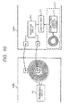
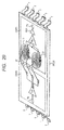
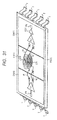
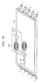
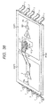
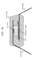
- Figs. 9 and 10 show typical layouts of the magnetic field change detection circuit 101.
- the coil of the magnetic field change detection circuit 101 should preferably be positioned close to the isolation element ISO1 so that the coil will be exposed to magnetic fields at a level equivalent to that of the magnetic fields sustained by the isolation element ISO1.
- Fig. 10 shows a typical layout in which the isolation element ISO1 is formed on the side of the semiconductor chip CHP0.
- the pulse width detection circuit 102 is a circuit that detects whether the interval between logical value changes in the reproduced transmission data VIN (i.e., output data VOUT) has become longer than a predetermined interval. In other words, the pulse width detection circuit 102 detects whether the pulse width of the output data VOUT has become greater than a predetermined width. Ordinarily, the signal for controlling the power transistor PTr1 is PWM-modulated so that its pulse width does not become greater than the predetermined width. That is, the power transistor PTr1 is not kept turned on longer than the predetermined interval. If the pulse width of the output data VOUT is greater than the predetermined width, there is a possibility that a malfunction has occurred in signal transmission via the isolation element ISO1. For that reason, if the pulse width of the output data VOUT turns out to be greater than the predetermined width, the pulse width detection circuit 102 determines that an abnormality that can cause a malfunction in signal transmission via the isolation element ISO1 has occurred.
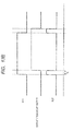
- Fig. 11A shows a typical configuration of the pulse width detection circuit 102.
- Fig. 11B is a timing chart showing typical operations of the pulse width detection circuit 102.
- the pulse width detection circuit 102 includes an isolation part 1021, a pulse detection part 1022, an OR circuit 1023, and a timer 1024.
- the pulse detection part 1022 has comparators 1025 through 1027.
- the isolation part 1021 is configured the same as the isolation element ISO1.
- the isolation part 1021 forwards the transmission signal from the transmission circuit Tx1 to the pulse detection part 1022 as reception signals (Sig+, Sig-).
- the comparator 1025 outputs the result of the comparison reflecting the potential difference between the reception signals (Sig+, Sig-) from the isolation part 1021.
- the comparator 1026 compares the threshold voltage Vth+ on the high-level side with the comparison result from the comparator 1025 and outputs the result of the comparison.
- the comparator 1027 compares the threshold voltage Vth- on the low-level side with the comparison result from the comparator 1025 and outputs the result of the comparison.
- the OR circuit 1023 outputs the OR of the comparison result from the comparator 1026 and of the comparison result from the comparator 1027 as a reset signal RST.
- the reset signal RST is driven high every time a positive amplitude pulse signal and a negative amplitude pulse signal are transmitted as reception signals.
- the timer 1024 performs a count operation in synchronism with a clock signal CLK for counting purposes.
- the timer 1024 performs a count operation based on a constant current or a constant voltage for driving a time constant circuit.
- the timer 1024 outputs a high-level detection result E2; otherwise the timer 1024 outputs a low-level detection result E2.
- the timer 1024 resets the count value to "0" in synchronism with a rising edge of the reset signal RST.
- the timer 1024 resets the count value to "0" before the count value reaches the threshold value. Consequently the detection result E1 is kept at the low level.
- the detection result E2 becomes high because the count value on the timer 1024 has reached the threshold value.
- the pulse width detection circuit 102 determines that any abnormality that can cause a malfunction in signal transmission via the isolation element ISO1 has not occurred, and outputs the low-level detection result E2. On the other hand, if the interval between logical value changes in the reproduced transmission data VIN (output data VOUT) exceeds the predetermined interval, the pulse width detection circuit 102 determines that an abnormality that can cause a malfunction in signal transmission via the isolation element ISO1 has occurred and outputs the high-level detection result E2.
- the pulse width detection circuit 102 can detect abnormalities not only when the transformer is used as the isolation element ISO1 but also where the capacitor, GMR element isolator, or photo-coupler is utilized as the isolation element ISO1. In these cases, the configuration of the isolation part 1021 is changed in keeping with the configuration of the isolation element ISO1. For example, if the capacitor is used as the isolation part ISO1, the isolation part 1021 is replaced with an isolation part 1028 comprised of a capacitor as shown in Fig. 12 .
- Fig. 13A shows another typical configuration of the pulse width detection circuit 102 as a pulse width detection circuit 102a.
- Fig. 13B is a timing chart showing typical operations of the pulse width detection circuit 102a.
- the pulse width detection circuit 102a includes a logical value change detection circuit 1028 and a timer 1024.
- the logical value change detection circuit 1028 has a delay buffer 1029 and an exclusive-OR circuit 1030.
- the delay buffer 1029 outputs the output data VOUT from the reception circuit Rx1 after delaying it by a predetermined time period Td.
- the exclusive-OR circuit 1030 outputs the exclusive-OR of the output data VOUT and of the output from the delay buffer 1029 as a reset signal RST.
- the exclusive-OR circuit 1030 drives the reset signal RST high in response to a logical value change in the output data VOUT and drives the reset signal RST low upon elapse of the predetermined time period Td. That is, the logical value change detection circuit 1028 drives the reset signal RST high every time the output data VOUT develops a logical value change.
- the pulse width detection circuit 102a shown in Fig. 13A also provides the same effects as the pulse width detection circuit 102 in Fig. 11A .
- the pulse width detection circuit 102a has no need for an isolation part and thus can minimize the increase in circuitry size.
- the pulse width detection circuit 102a is easier to configure than the pulse width detection circuit 102.
- the pulse width detection circuit 102a can be used as the abnormality detection part regardless of the type of the isolation element ISO1 in use. That means the pulse width detection circuit 102a can also be used as the abnormality detection part in conjunction with a non-pulse time isolation element such as the photo-coupler.
- the configuration shown in Fig. 13A is not limitative of the pulse width detection circuit 102a; the pulse width detection circuit 102a may be configured differently while still offering equivalent functions.
- the common mode noise detection circuit 103 is a circuit that detects whether common mode noise has exceeded a predetermined threshold range.
- Common mode noise refers to the noise generated due to the voltage difference (i.e., common mode voltage) between two power sources, one power source driving one semiconductor chip and the other power source driving another semiconductor chip.
- the common mode noise is the noise of which the cause is attributable to the voltage difference (common mode voltage) between a first power source (e.g., ground voltage GND0) driving the semiconductor chip CHP0 and a second power source (e.g., ground voltage GND1) driving the semiconductor chip CHP1.
- the common mode noise detection circuit 103 determines that an abnormality that can cause a malfunction in signal transmission via the isolation element ISO1 has occurred.
- Fig. 14A is a typical configuration of the common mode noise detection circuit 103.
- Fig. 14B is a timing chart showing typical operations of the common mode noise detection circuit 103.
- the common mode noise detection circuit 103 shown in Fig. 14A includes an isolation part 1031, an adder circuit 1032, comparators 1033 and 1034, and an OR circuit 1035.
- the isolation part 1031 is configured the same as the isolation element ISO1.
- the isolation part 1031 forwards the transmission signal from the transmission circuit Tx1 to the adder circuit 1032 as reception signals (Sig+, Sig-).
- the adder circuit 1032 adds up the voltage of the reception signal (Sig+) and that of the reception signal (Sig-) to output a sum result SigSum.
- the comparator 1033 compares the threshold voltage Vth+ on the high-level side with the sum result SigSum from the adder circuit 1032 and outputs the result of the comparison.
- the comparator 1034 compares the threshold voltage Vth- on the low-level side with the sum result SigSum from the adder circuit 1032 and outputs the result of the comparison.
- the OR circuit 1035 outputs the OR of the comparison result from the comparator 1033 and of the comparison result from the comparator 1034 as a detection result E3.
- the adder circuit 1032 gets the pulse signal overlaid on the reception signal (Sig+) and the pulse signal overlaid on the reception signal (Sig-) to cancel out each other, and adds up the in-phase common mode voltages overlaid on the reception signals (Sig+, Sig-) to output the sum. That is, the sum result SigSum from the adder circuit 1032 is a signal on which only the common mode voltage component is overlaid. If the sum result SigSum is higher than the threshold voltage Vth+, the comparator 1033 outputs a high-level comparison result; otherwise the comparator 1033 outputs a low-level comparison result.
- the comparator 1034 If the sum result SigSum is lower than the threshold voltage Vth-, the comparator 1034 outputs a high-level comparison result; otherwise the comparator 1034 outputs a low-level comparison result. Thus if the sum result SigSum exceeds the threshold voltage range of Vth- through Vth+, the OR circuit 1035 outputs a high-level detection result E3; otherwise the OR circuit 1035 outputs a low-level detection result E3.
- the common mode noise detection circuit 103 determines that any abnormality that can cause a malfunction in signal transmission via the isolation element ISO1 has not occurred and outputs the low-level detection result E3. On the other hand, if the common mode noise exceeds the predetermined threshold range, the common mode noise detection circuit 103 determines that an abnormality that can cause a malfunction in signal transmission via the isolation element ISO1 has occurred and outputs the high-level detection result E3.
- the common mode noise detection circuit 103 can detect abnormalities not only when the transformer is used as the isolation element ISO1 but also where the capacitor, GMR element isolator, or photo-coupler is utilized as the isolation element ISO1. In these cases, the configuration of the isolation part 1031 is changed in keeping with the configuration of the isolation element ISO1. For example, if the capacitor is used as the isolation part ISO1, the isolation part 1031 is replaced with an isolation part 1036 comprised of a capacitor as shown in Fig. 15 .
- Fig. 16 is a circuit diagram showing another typical configuration of the common mode noise detection circuit 103 in the form of a common mode noise detection circuit 103a.
- the common mode noise detection circuit 103a shown in Fig. 16 includes a capacitor 1037 used as the isolation element, resistance elements 1038 and 1039, and a comparator 1040.
- One electrode of the capacitor 1037 is supplied via the resistance element 1038 with the ground voltage GND0 that is the first power source.
- the other electrode of the capacitor 1037 is fed via the resistance element 1039 with the ground voltage GOD1 that is the second power source.
- the comparator 1040 compares a predetermined threshold voltage with the voltage on the other electrode (on the second power source side) of the capacitor 1037 and outputs the result of the comparison (comparison result E3). Specifically, if the voltage on the other electrode of the capacitor 1037 is higher than the threshold voltage, the comparator 1040 outputs the high-level detection result E3; otherwise the comparator 1040 outputs the low-level comparison result E3.
- the capacitor 1037 can also incur an inter-power-source noise. This causes the voltage on the other electrode of the capacitor 1337 to fluctuate.
- the common mode noise detection circuit 103a shown in Fig. 16 determines that an abnormality that can cause a malfunction in signal transmission via the isolation element ISO1 has occurred if the capacitor 1037 has generated the inter-power-source noise (common mode noise) causing the other electrode (second power source side) of the capacitor 1037 to carry a voltage higher than the threshold voltage.
- the common mode noise detection circuit 103a shown in Fig. 16 determines that an abnormality that can cause a malfunction in signal transmission via the isolation element ISO1 has occurred.
- the common mode noise detection circuit 103a also provides the same effects as the common mode noise detection circuit 103 shown in Fig. 14A .
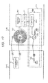
- Figs. 17 and 18 show typical layouts of the common mode noise detection circuit 103a.
- the capacitor 1037 of the common mode noise detection circuit 103a should preferably be positioned close to the isolation element ISO1 so that the noise may be generated under conditions as similar as possible to those for the isolation element ISO1.
- Fig. 18 shows a layout example in which both the isolation element ISO1 and the capacitor 1037 are formed on the side of the semiconductor chip CHP0.
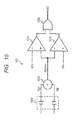
- Fig. 19A is a circuit diagram showing yet another typical configuration of the common mode noise detection circuit 103 in the form of a common mode noise detection circuit 103b.
- Fig. 19B is a timing chart showing typical operations of the common mode noise detection circuit 103b.
- the common mode noise detection circuit 103b includes an isolation part 1031, a low-pass filter 1041, comparators 1033 and 1034, and an OR circuit 1035.
- the isolation part 1031 forwards the transmission signal from the transmission circuit Tx1 as a reception circuit Sig+ (voltage at one end of the secondary side coil).
- the low-pass filter 1041 extracts the common mode noise component overlaid on the reception signal Sig+ and outputs the extracted component as a signal SigLPF.
- the comparator 1033 If the signal SigLPF from the low-pass filter 1041 is higher than the threshold voltage Vth+ on the high-level side, the comparator 1033 outputs a high-level comparison result; otherwise the comparator 1033 outputs a low-level comparison result. If the signal SigLPF from the low-pass filter 1041 is lower than the threshold voltage Vth- on the low-level side, the comparator 1034 outputs a high-level comparison result; otherwise the comparator 1034 outputs a low-level comparison result.
- the OR circuit 1035 outputs the high-level detection result E3; otherwise the OR circuit 1035 outputs the low-level detection result E3.
- the common mode noise detection circuit 103b shown in Fig. 19A also provides the same effects as the common mode noise detection circuit 103 in Fig. 14A .
- control part CT1 was explained as outputting the stop signal only if the abnormality detection part DT1 has detected an abnormality.
- the control part CT1 may be configured differently so as to output the stop signal not only when the abnormality is detected by the abnormality detection part DT1 but also where other abnormalities are detected.
- Fig. 20 shows a variation of the semiconductor integrated circuit 1, i.e., a configuration of the semiconductor integrated circuit 1 supplemented with an abnormality detection part DTX1 for detecting other abnormalities.
- Fig. 20 shows only the abnormality detection circuit DT1, abnormality detection circuit DTX1, and an OR circuit 111. The ensuing explanation will primarily deal with the configuration and operations of the abnormality detection part DTX1.
- the abnormality detection part DEX1 shown in Fig. 20 includes a power-on reset circuit 105, a low-voltage detection circuit 106, a power source noise detection circuit 107, an overcurrent detection circuit 108, an overheat detection circuit 109, and an OR circuit 110 that outputs the OR of the detection results from these circuits as a detection result EX0.
- the abnormality detection part DTX1 When at least one of these detection circuits detects an abnormality, the abnormality detection part DTX1 outputs a high-level detection result EX0; when none of the detection circuits detects an abnormality, the abnormality detection part DTX1 outputs a low-level detection result Ex0.
- the abnormality detection part DT1 outputs the detection result E0.
- the OR circuit 111 outputs the OR of the detection result E0 from the abnormality detection part DT1 and of the detection result EX0 from the abnormality detection part DTX1 as a detection result ER1.
- Fig. 21 shows typical relations of coupling among the abnormality detection parts DT1 and DTX1, control part CT1, and their peripheral circuits.
- the power-on reset circuit 105 is a circuit that detects a predetermined time period over which the source voltage VDD1 on the side of the semiconductor chip CHP1 stabilizes after power-on. Immediately after power is turned on, the source voltage VDD1 is unstable so that the circuits powered thereby may not operate normally for a certain period. Thus during a predetermined time period following power-on, the power-on reset circuit 105 determines that an abnormality is taking place.
- Fig. 22 shows a typical configuration of the power-on reset circuit 105.
- Fig. 23 is a timing chart showing typical operations of the power-on reset circuit 105.
- the power-on reset circuit 105 includes a resistance element 1051, a capacitor 1052, and an inverter 1053.
- the resistance element 1051 is provided interposingly between the source voltage terminal to which the source voltage VDD1 is supplied (the terminal is called the source voltage terminal VDD1 hereunder) and a node N1.
- the capacitor 1052 is provided interposingly between the node N1 and the ground voltage terminal to which the ground voltage GND1 is supplied (the terminal is called the ground voltage terminal GND1 hereunder).
- the inverter 1053 outputs the high-level detection result E1 (from time t1 to time t2).
- the inverter 1053 outputs the low-level detection result E5 (at time t2).
- the power-on reset circuit 105 outputs the high-level detection result E5 after power is applied and until a predetermined time period elapses. Upon elapse of the predetermined time period, with the source voltage stabilized, the power-on reset circuit 105 outputs the low-level detection result E5.
- the low-voltage detection circuit 106 is a circuit that detects whether the voltage level of the source voltage VDD1 on the side of the semiconductor chip CHP1 is lower than a predetermined threshold value. While the source voltage VDD1 is being lower than the threshold value, the circuits powered thereby may not operate normally. Thus if the voltage level of the source voltage VDD1 becomes lower than the threshold value, the low-voltage detection circuit 106 determines that an abnormality has occurred.
- Fig. 24 shows a typical configuration of the low-voltage detection circuit 106.
- Fig. 25 is a graphic representation explanatory of the workings of the low-voltage detection circuit 106.
- Fig. 26 is a timing chart showing typical operations of the low-voltage detection circuit 106.
- the low-voltage detection circuit 106 shown in Fig. 24 includes a reference voltage generation circuit 1061, comparators 1062 and 1063, and an RS latch 1064. Shown in Fig. 24 is the configuration example in which the voltage level of the source voltage VDD1 at stable time is 5V.
- the reference voltage generation circuit 1061 generates a first reference voltage of 4V and a second reference voltage of 4.5V, for example.
- the comparator 1062 compares the source voltage VDD1 with the first reference voltage and outputs the result of the comparison.
- the comparator 1063 compares the source voltage VDD1 with the second reference voltage and outputs the result of the comparison.
- the RS latch 1064 outputs from an output terminal Q a detection result E6 based on the comparison result coming from the comparator 1062 and input to a set terminal S and on the comparison result sent from the comparator 1063 and input to a reset terminal R.
- the comparator 1062 when the voltage level of the source voltage VDD1 is lower than 4.0V (at time t0), the comparator 1062 outputs a high-level comparison result and the comparator 1063 outputs a low-level comparison result. This causes the RS latch 1064 to output a high-level detection result E6.
- the comparator changes its comparison result to the low level but the comparator 1063 holds its low-level comparison result unchanged. This causes the RS latch 1064 to keep outputting the high-level detection result.
- the comparator 1063 changes its comparison result to the high level. This causes the RS latch 1064 to change its detection result E6 to the low-level and output the low-level detection result E6.
- the comparator 1063 changes its comparison result to the low level but the comparator 1062 holds its low-level comparison result unchanged. This causes the RS latch 1064 to keep outputting the low-level detection result E6.
- the comparator 1062 changes its comparison result to the high level. This causes the RS latch 1064 to changes its detection result E6 to the high level and output the high-level detection result E6. That is, the low-voltage detection circuit 106 provides the detection of the source voltage VDD1 with a hysteresis characteristic (see Fig. 25 ).
- the low-voltage detection circuit 106 determines that the source voltage VDD1 is stable and outputs the low-level detection result E6.
- the low-level detection circuit 106 determines that the source voltage VDD1 is unstable and outputs the high-level detection result E6.
- the power source noise detection circuit 107 is a circuit that detects whether the noise of the source voltage VDD1 on the side of the semiconductor chip CHP1 has exceeded a predetermined threshold range. If the noise of the source voltage VDD1 exceeds the threshold range, the circuits powered thereby may not operate normally. Thus if the noise of the source voltage VDD1 has exceeded the threshold range, the power source noise detection circuit 107 determines that an abnormality has occurred.
- Fig. 27 shows a typical configuration of the power source noise detection circuit 107.
- Fig. 28 is a timing chart showing typical operations of the power source noise detection circuit 107.
- the power source noise detection circuit 107 shown in Fig. 27 includes a capacitor 1071, an operation amplifier 1072, a resistance element 1073, comparators 1074 and 1075, and an OR circuit 1076.
- the capacitor 1071 is provided interposingly between the source voltage terminal VDD1 and the operation amplifier 1072.
- the resistance element 1073 is provided interposingly between the output and the input terminals of the operation amplifier 1072. That is, the capacitor 1071, operation amplifier 1072, and resistance element 1073 make up a so-called high-pass filter.
- the comparator 1074 compares the threshold voltage Vth+ on the high-level side with the output voltage from the operation amplifier 1072 and outputs the result of the comparison.
- the comparator 1075 compares the threshold voltage Vth- on the low-level side with the output voltage from the operation amplifier 1072 and outputs the result of the comparison.
- the OR circuit 1076 outputs the OR of the comparison result from the comparator 1074 and of the comparison result from the comparator 1075 as a detection result E7.
- the power source noise detection circuit 107 determines that the source voltage VDD1 is stable and outputs a low-level detection result E7.
- the power source noise detection circuit 107 determines that the source voltage VDD1 is unstable and outputs a high-level detection result E7.
- the overcurrent detection circuit 108 is a circuit that detects whether an overcurrent flows through the power transistor PTr1. If the current value of the current flowing through the power transistor PTr1 is larger than a predetermined threshold value, the power transistor PTr1 may be destroyed or otherwise damaged. Thus if the current value of the current flowing through the power transistor PTr1 becomes larger than the predetermined threshold value, the overcurrent detection circuit 108 determines that an abnormality has occurred and outputs a high-level detection result E8.
- the overheat detection circuit 109 is a circuit that detects whether the temperature inside or around the semiconductor chip CHP1 has become higher than a predetermined threshold temperature. If the temperature becomes higher than the threshold value, the circuits may operate normally. Thus if the temperature inside or around the semiconductor chip CHP1 is higher than the predetermined threshold temperature, the overheat detection circuit 109 determines that an abnormality has occurred and outputs a high-level detection result E9. For example, the overheat detection circuit 109 may detect the temperature based on the value of a forward voltage Vf of diodes located near the object of which the temperature is to be measured.
- Figs. 29 through 40 show packaged states in which a transformer is used as the isolation element ISO1
- Figs. 36 and 37 show packaged state in which a capacitor is used as the isolation element ISO1.
- Fig. 38 shows a packaged state in which a GMR element isolator is used as the isolation element ISO1.
- Figs. 39 and 40 show packaged states in which a photo-coupler is used as the isolation element ISO1.
- Figs. 29 through 40 are provided primarily for the purpose of explaining how the transmission circuit Tx1, reception circuit Rx1, and isolation element ISO1 interposed therebetween are packaged. As such, Figs. 29 through 40 do not show the control part CT1 and abnormality detection part DT1.
- the transmission circuit Tx1 is formed over the semiconductor chip CHP0.
- the semiconductor chip CHP1 includes the reception circuit Rx1, primary side coil L11 and secondary side coil L12 making up the isolation element ISO1, and gate driver GD1. Also, the semiconductor chip CHP0 has a plurality of pads formed and coupled to the output of the transmission circuit Tx1.
- the semiconductor chip CHP1 has pads formed and coupled to both ends of the primary side coil L11. By way of these pads and bonding wires W, the transmission circuit Tx1 is coupled to the primary side coil L11 formed over the semiconductor chip CHP1.
- the center tap of the primary side coil L11 is coupled to the power supply terminal on the side of the semiconductor chip CHP0 (e.g., ground voltage terminal GND0) by way of a pad and a bonding wire w separately provided.
- the center tap of the secondary side coil L12 is coupled to the power supply terminal on the side of the semiconductor chip CHP1 (e.g., ground voltage terminal GND1).
- the primary side coil L11 and secondary side coil L12 are formed in a first wiring layer and a second wiring layer, respectively, which are stacked one on top the other over one semiconductor chip.
- the primary side coil L11 is formed by two coils with the center tap interposed therebetween, and the secondary side coil L12 is also formed by two coils with the center tap interposed therebetween.
- the transmission circuit Tx1 and the primary side coil L11 and secondary side coil L12 making up the isolation element ISO1 are formed over the semiconductor chip CHP0.
- the reception circuit Rx1 and gate driver GD1 are formed over the semiconductor chip CHP1.
- the semiconductor chip CHP0 has pads formed and coupled to both ends of the secondary side coil L12.
- the semiconductor chip CHP1 has pads formed and coupled to the input of the reception circuit Rx1. By way of these pads and bonding wires W, the reception circuit Rx1 is coupled to the secondary side coil L12 formed over the semiconductor chip CHP0.
- the primary side coil L11 and secondary side coil L12 are formed in a first wiring layer and a second wiring layer, respectively, which are stacked one on top the other over one semiconductor chip.
- the transmission circuit Tx1 is formed over the semiconductor chip CHP0.
- the reception circuit Rx1 and gate driver GD1 are formed over the semiconductor chip CHP1.
- the primary side coil L11 and secondary coil L12 making up the isolation element ISO1 are formed over a semiconductor chip CHP3 different from the semiconductor chips CHP0 and CHP1.
- the semiconductor chip CHP0 has pads formed and coupled to the output of the transmission circuit Tx1.
- the semiconductor chip CHP1 has pads formed and coupled to the input of the reception circuit Rx1.
- the semiconductor chip CHP3 has pads formed and coupled to the two ends of the primary side coil L11 as well as pads formed and coupled to both ends of the secondary side coil L12.
- the transmission circuit Tx1 is coupled to the primary side coil L11 formed over the semiconductor chip CHP3. Also via these pads and bonding wires W, the reception circuit Rx1 is coupled to the secondary side coil L12 formed over the semiconductor chip CHP3.
- the primary side coil L11 and secondary side coil L12 are formed in a first wiring layer and a second wiring layer, respectively, which are stacked one on top the other over one semiconductor chip.
- the transmission circuit Tx1 and primary side coil L1 are formed over the semiconductor chip CHP0
- the reception circuit Rx1, gate driver GD1, and secondary side coil L12 are formed over the semiconductor chip CHP1.
- the semiconductor chips CHP0 and CHP1 are stacked one on top the other. When stacked, the semiconductor chips CHP0 and CHP1 are positioned in such a manner that the center of the primary side coil L11 and that of the secondary side coil L12 are on the same straight line.
- the transmission circuit Tx1, reception circuit Rx1, primary side coil L11 and secondary side coil L12 making up the isolation element ISO1, and gate driver GD1 are formed over a common semiconductor chip CHP4.
- the primary side coil L11 and secondary side coil L12 are formed in a first wiring layer and a second wiring layer, respectively, which are stacked one on top the other over the semiconductor chip CHP4.
- the area in which the transmission circuit Tx1 is located and the area in which the reception circuit Rx1 are positioned are isolated from each other by an isolation layer formed in the substrate of the semiconductor chip CHP4.
- Figs. 34 and 35 are cross-sectional views of the substrate carrying the semiconductor chip CHP4 shown in Fig. 33 .
- the area in which the transmission circuit Tx1 is formed and the area in which the reception circuit Rx1 are formed are cut off electrically from each other by an isolation layer.
- the primary side coil L11 and secondary side coil L12 are provided in the area where the reception circuit Rx1 is formed.
- the area in which the transmission circuit Tx1 is formed and the area in which the reception circuit Rx1 are formed are also cut off electrically from each other by an isolation layer.
- the primary side coil L11 and secondary side coil L12 are provided in the area where the transmission circuit Tx1 is formed.
- Fig. 36 shows the packaged state of Fig. 2 in which the transformer is replaced with a capacitor as the isolation element ISO1. More specifically, the coil L11 is replaced with one electrode C11 of the capacitor and the coil L12 with the other electrode C12 thereof.
- Fig. 37 shows the packaged state of Fig. 29 in which the transformer is replaced with a capacitor as the isolation element ISO1. More specifically, the coil L11 is replaced with electrodes C11a and C11b on one side of the capacitor and the C12 with electrodes C12a and C12b on the other side thereof.
- Fig. 37 shows the packaged state of Fig. 2 in which the transformer is replaced with a GMR element isolator as the isolation element ISO1. More specifically, the coil L11 is left intact while the coil L12 is replaced with a GMR element R12.
- a light emitting element D11 is formed over the semiconductor chip CHP0 while a light receiving part Q12, the reception circuit Rx1, and gate driver GD1 are formed over the semiconductor chip CHP1.
- the light emitting element D11 and light receiving part Q12 make up the photo-coupler.
- Fig. 40 is a cross-sectional view of the semiconductor integrated circuit shown in Fig. 39 .
- the semiconductor chip CHP0 carrying the light emitting element D11 and the semiconductor chip CHP1 carrying the light receiving part Q12 are stacked one on top the other.
- the semiconductor chips CHP0 and CHP1 are positioned so that the light emitting element D11 and light receiving part Q12 are faced with each other.
- the gap between the light emitting element D11 and the light receiving element Q12 is filled with a transparent resin material permitting transmission of light signals from the light emitting element D11 to the light receiving part Q12.
- the entire assembly is enclosed by a plastic mold that keeps the light signals of the light emitting element D11 from leaking out.
- the isolation element ISO1 As explained above, there are no specific constraints on the type of the isolation element ISO1 or on the layout thereof. Whereas the foregoing paragraphs showed the isolation element ISO1 formed over a semiconductor chip, the isolation element ISO1 may be provided alternatively as an external part.
- Fig. 41 is a timing chart showing typical operations of the semiconductor integrated circuit 1 operating on a signal transmission method different from that shown in Fig. 3 .
- the signal transmission method shown in Fig. 41 may be adopted when the AC coupling element such as the transformer, capacitor, or GMR isolator is used as the isolation element ISO1.
- the signal transmission method shown in Fig. 41 is used not only for the transmission of signals via the isolation element ISO1 but also for signal transmission via other isolation elements, to be discussed later.
- the transmission circuit Tx1 outputs two consecutive pulse signals (called a two-pulse signal altogether) as a transmission signal in synchronism with a rising edge of transmission data VIN.
- the transmission circuit Tx1 also outputs a single pulse signal (called a one-pulse signal) as another transmission signal in synchronism with a falling edge of the transmission data VIN.
- the isolation element ISO1 forwards the transmission signal coming from the transmission circuit Tx1 to the reception circuit Rx1 as a reception signal.
- the reception circuit Rx1 drives output data VOUT high; upon receipt of the one-pulse signal as the reception signal, the reception circuit Rx1 drives the output data VOUT low. In this manner, the reception circuit Rx1 reproduces the transmission data VIN and outputs the reproduced data as the output data VOUT.
- the reception circuit Rx1 has a high-level detection circuit, a low-level detection circuit, and an RS latch, for example.
- the high-level detection circuit drives a set signal high.
- the low-level detection circuit drives a reset signal high.
- the RS latch Based on the set signal from the high-level detection circuit and on the reset signal from the low-level detection circuit, the RS latch outputs the output data VOUT. That is, the RS latch drives the output data VOUT high upon receipt of the two-pulse signal and drives the output data VOUT low on receiving the one-pulse signal.
- the transmission data VIN changes from high level to low level at time t1.
- This causes the transmission circuit Tx1 to output the two-pulse signal as the transmission signal (at time t1).
- the reception circuit Rx1 drives the output data VOUT high (time t2) .
- any abnormality that may cause a malfunction signal transmission via the isolation element ISO1 has not occurred, so that the abnormality detection part DT1 outputs a low-level detection result ER1.
- the control part CT1 outputs the output data VOUT from the reception circuit Rx1 unchecked. Because the output data VOUT is at the high level, the gate control signal OUT is also high, which turns on the power transistor PTr1.
- the abnormality detection part DT1 outputs a high-level detection result ER1 as long as the abnormality is present (from time t3 to time t4).
- the control part CT1 outputs a low-level stop signal regardless of the output data VOUT (i.e., regardless of the transmission data VIN). This drives the gate control signal OUT low, which forcibly turns off the power transistor PTr1.
- the abnormality detection part DT1 changes the detection result ER1 from high level to low level (at time t4). This causes the control part CT1 to again start outputting the output data VOUT from the reception circuit Rx1 unchecked. That is, the control part CT1 cancels the stop signal. Because the output data VOUT is at the high level, the gate control signal OUT also becomes high, which turns on the power transistor PTr1 (at time t4).
- the transmission data VIN changes from high level to low level at time t5.
- the reception circuit Rx1 drives the output data VOUT low (at time t6).
- the abnormality detection part DT1 outputs a low-level detection result ER1.
- the control part CT1 outputs the output data VOUT from the reception circuit Rx1 unchecked. Since the output data VOUT is at the low level, the gate control signal OUT also becomes low, which turns off the power transistor PTr1.
- the abnormality detection part DT1 outputs a high-level detection result ER1 as long as the abnormality is present (from time t7 to time t8).
- the control part CT1 outputs a low-level stop signal regardless of the output data VOUT (i.e., regardless of the transmission data VIN). This drives the gate control signal OUT low, which forcibly turns off the power transistor PTr1. That is, the power transistor PTr1 is kept turned off.
- the abnormality detection part DT1 changes the detection result ER1 from high level to low level (at time t8). This causes the control part CT1 to again start outputting the output data VOUT from the reception circuit Rx1 unchecked. That is, the control part CT1 cancels the stop signal. Because the output data VOUT is at the low level, the gate control signal OUT also becomes low, which keeps the power transistor PTr1 off (at time t8).
- the semiconductor integrated circuit 1 adopting the signal transmission method of the second embodiment offers substantially the same effects as those of the first embodiment.
- control part CT1 furnished separately from the reception circuit Rx1.
- control part CT1 may be incorporated as part of the reception circuit Rx1.
- the control part CT1 may be incorporated as an OR circuit in the reception circuit Rx1.
- the OR circuit outputs the OR of the reset signal from the low-level detection circuit and of the detection result ER from the abnormality detection part DT1 to the reset terminal R of the RS latch.
- the reception circuit Rx1 keeps outputting the low-level output data VOUT until the next logical value change occurs in the transmission data VIN (see Fig. 42 ). In other words, after the abnormality detected by the abnormality detection part is no longer detected, the reception circuit Rx1 cancels the stop signal in synchronism with a first logical value change in the transmission data VIN.
- Fig. 43 is a timing chart showing typical operations of the semiconductor integrated circuit 1 operating on a signal transmission method different from that shown in Fig. 3 or in Fig. 41 .
- the signal transmission method shown in Fig. 43 may be adopted when the AC coupling element such as the transformer, capacitor, or GMR isolator is used as the isolation element ISO1.
- the signal transmission method shown in Fig. 43 is used not only for the transmission of signals via the isolation element ISO1 but also for signal transmission via other isolation elements, to be discussed later.
- the transmission circuit Tx1 outputs pulses not multiplexed on the transmission signal when the transmission data VIN is at the low level, and outputs consecutive pulses multiplexed on the transmission signal when the transmission data is at the high level.
- the isolation element ISO1 forwards the transmission signal coming from the transmission circuit Tx1 to the reception circuit Rx1 as the reception signal.
- the reception circuit Rx1 drives the output data VOUT high; upon receipt of the pulse-free reception signal, the reception circuit Rx1 drives the output data VOUT low. In this manner, the reception circuit Rx1 reproduces the transmission data VIN and outputs the reproduced data as the output data VOUT.
- the transmission data VIN is at the low level at time t0.
- the transmission circuit Tx1 outputs pulses not multiplexed on the transmission signal (at time t0).
- the reception circuit x1 outputs the low-level output data VOUT because it is receiving the pulse-free reception signal (at time t0).
- the transmission data VIN changes from low level to high level at time t1.
- the reception circuit Rx1 drives the output data high (at time t1).
- any abnormality that can cause a malfunction in signal transmission via the isolation element ISO1 has not occurred, so that the abnormality detection part DT1 outputs a low-level detection result ER1.
- the control part CT1 outputs the output data VOUT from the reception circuit Rx1 unchecked. Because the output data VOUT is at the high level, the gate control signal OUT is also high, which turns on the power transistor PTr1.
- the abnormality detection part DT1 outputs a high-level detection result ER1 as long as the abnormality is present (from time t2 to time t3).
- the control part CT1 outputs a low-level stop signal regardless of the output data VOUT (i.e., regardless of the transmission data VIN). This drives the gate control signal OUT low, which forcibly turns off the power transistor PTr1.
- the abnormality detection part DT1 changes the detection result ER1 from high level to low level (at time t3). This causes the control part CT1 to again start outputting the output data VOUT from the reception circuit Rx1 unchecked. Because the output data VOUT is at the high level, the gate control signal OUT also becomes high, which turns on the power transistor PTr1 (from time t3 to t4).
- the transmission data VIN changes from high level to low level at time t4.
- the reception circuit Rx1 drives the output data VOUT low (at time t4).
- any abnormality that can cause a malfunction in signal transmission via the isolation element ISO1 has not occurred, so that the abnormality detection part DT1 outputs a low-level detection result ER1.
- the control part CT1 outputs the output data VOUT from the reception circuit Rx1 unchecked. Because the output data VOUT is at the low level, the gate control signal OUT is also low, which turns off the power transistor PTr1.
- the abnormality detection part DT1 outputs a high-level detection result ER1 as long as the abnormality is present (from time t5 to time t6).
- the control part CT1 outputs a low-level stop signal regardless of the output data VOUT (i.e., regardless of the transmission data VIN). This drives the gate control signal OUT low, which forcibly turns off the power transistor PTr1. That is, the power transistor PTr1 is kept off.
- the abnormality detention part DT1 changes the detection result ER1 from high level to low level (at time t6). This causes the control part CT1 to again start outputting the output data VOUT from the reception circuit Rx1 unchecked. Because the output data VOUT is at the low level, the gate control signal OUT also becomes low, which keeps the power transistor PTr1 off (at time t6).
- the semiconductor integrated circuit 1 adopting the signal transmission method of the third embodiment offers substantially the same effects as those of the first embodiment.
- Fig. 44 shows a typical configuration of a semiconductor integrated circuit 2 as the fourth embodiment of the present invention.
- the semiconductor integrated circuit 2 in Fig. 44 has an abnormality detection part DT2 and a control part CT2 which are formed over the semiconductor chip CHP0 and which replace the abnormality detection part DT1 and control part CT1, respectively, formed over the semiconductor chip CHP1. That is, the abnormality detection part and control part are provided over the chip on the side of the transmission circuit Tx1.
- the ensuing paragraphs will mainly explain the configurations and operations of the abnormality detection part DT2 and control part CT2.
- the abnormality detection part DT2 has substantially the same circuit configuration as the abnormality detection part DT1.
- the abnormality detection part DT2 detects an abnormality that can cause a malfunction in signal transmission via the isolation element ISO1 and outputs a detection result ER2 upon such detection. For example, upon detecting an abnormality, the abnormality detection part DT2 outputs a high-level detection result ER2; when not detecting any abnormality, the abnormality detection part DT2 outputs a low-level detection result ER2.
- the abnormality detection part DT2 includes a magnetic field change detection circuit 201, a pulse width detection circuit 202, and a common mode noise detection circuit 203, not shown.
- the control part CT2 has substantially the same circuit configuration as the control part CT1.
- the control part CT2 outputs a stop signal to turn off the power transistor PTr1 regardless of externally supplied transmission data VIN.
- the control part CT2 outputs the externally supplied transmission data VIN unchecked to the transmission circuit Tx1. This allows the conduction state of the power transistor PTr1 to be controlled in accordance with the transmission data VIN.
- the control part CT2 outputs a low-level stop signal to the transmission circuit Tx1 regardless of the externally supplied transmission data VIN. This causes the transmission circuit Tx1 to convert the low-level stop signal to the transmission signal and to output the signal.
- the transmission signal from the transmission circuit Tx1 is forwarded to the reception circuit Rx1 as the reception signal via the isolation element ISO1. Consequently the power transistor PTr1 is controlled to be turned off.
- the configuration and operations of the magnetic field change detection circuit 201 are substantially the same as those of the magnetic field change detection circuit 101 and thus will not be discussed further.
- the pulse width detection circuit 202 is a circuit that detects whether the interval between logical value changes in the transmission data VIN supplied from another semiconductor chip has become longer than a predetermined interval. In other words, the pulse width detection circuit 202 detects whether the pulse width of the PWM-modulated transmission data VIN fed from another semiconductor chip has become greater than a predetermined width.
- the remaining details of the configuration and operations of the pulse width detection circuit 202 are the same as those of the pulse width detection circuit 102 and thus will not be discussed further.
- the common mode noise detection circuit 203 is a circuit that detects whether common mode noise has exceeded a predetermined threshold range.
- the comparator 1040 was shown furnished on the side of the other electrode (second power source side) of the capacitor 1037.
- the comparator 1040 is shown provided on the side of one electrode (first power source side) of the capacitor 1037.
- the remaining details of the configuration and operations of the common mode noise detection circuit 203 are the same as those of the common mode noise detection circuit 103a and thus will not be discussed further.
- the abnormality detection part DT2 may be configured differently in such a manner that, as a circuit for detecting an abnormality that can cause a malfunction in signal transmission via the isolation element ISO1, the part DT2 may include a power-on reset circuit 205, a low-voltage detection circuit 206, a power source noise detection circuit 207, and an overheat detection circuit 209 in addition to the above-mentioned three detection circuits.
- the power-on reset circuit 205, low-voltage detection circuit 206, power source noise detection circuit 207, and overheat detection circuit 209 correspond to the power-on reset circuit 105, low-voltage detection circuit 106, power source noise detection circuit 107, and overheat detection circuit 109, respectively.
- the power-on reset circuit 205 is a circuit that detects a predetermined time period over which the source voltage VDD0 on the side of the semiconductor chip CHP0 stabilizes after power-on. The remaining details of the configuration and operations of the power-on reset circuit 205 are the same as those of the power-on reset circuit 105 and thus will not be discussed further.
- the low-voltage detection circuit 206 is a circuit that detects whether the voltage level of the source voltage VDD0 on the side of the semiconductor chip CHP0 has become lower than a predetermined threshold value. The remaining details of the configuration and operations of the low-voltage detection circuit 206 are the same as those of the low-voltage detection circuit 106 and thus will not be discussed further.
- the power source noise detection circuit 207 is a circuit that detects whether the noise of the source voltage VDD0 on the side of the semiconductor chip CHP0 has exceeded a predetermined threshold range. The remaining details of the configuration and operations of the power source noise detection circuit 207 are the same as those of the power source noise detection circuit 107 and thus will not be discussed further.
- the overheat detection circuit 209 is a circuit that detects whether the temperature inside or around the semiconductor chip CHP0 has become higher than a predetermined threshold temperature. The remaining details of the configuration and operations of the overheat detection circuit 209 are the same as those of the overheat detection circuit 109 and thus will not be discussed further.
- the semiconductor integrated circuit 2 of the fourth embodiment turns off the power transistor PTr1 that is the target to be controlled.
- the inventive semiconductor integrated circuit 2 thus prevents the power transistor PTr1 from getting inadvertently turned on and thereby forestalls the malfunction of the load.
- the abnormality detection part DT2 may feed the detection result ER2 back to an external microcomputer.
- the microcomputer may again output the transmission data VIN of the same value.
- the microcomputer may output as the transmission data VIN a stop signal (low-level signal) that turns off the power transistor PTr1.
- Fig. 47 is a timing chart showing typical operations of the semiconductor integrated circuit 2 in Fig. 46 .
- the gate control signal OUT is controlled to be at the low level (i.e., the power transistor PTr1 is controlled to be off) regardless of the transmission data VIN.
- Fig. 48 is a block diagram showing a typical configuration of a semiconductor integrated circuit 3 as the fifth embodiment of the present invention.
- the semiconductor integrated circuit 3 shown in Fig. 48 includes a comparison part CMP1 that compares the logical value of the gate control signal OUT from the gate driver GD1 with the logical value of the transmission data VIN corresponding to the gate control signal OUT in question.
- the comparison part CMP1 also functions as an abnormality detection part detecting an abnormality that can cause a malfunction in signal transmission via the isolation element IS01.
- the comparison part CMP1 determines that an abnormality that may possibly cause a malfunction in signal transmission via the isolation element ISO1 has occurred.
- the semiconductor integrated circuit 3 in Fig. 48 has the comparison part CMP1 replacing the abnormality detection part DT2 and further includes a transmission circuit (second transmission circuit) Tx2, a reception circuit (second reception circuit) Rx2, and an isolation element (second isolation element) ISO2.
- the comparison part CMP1 also serves as the abnormality detection part.
- the transmission circuit Tx2 is formed along with the reception circuit Rx1 over the semiconductor chip CHP1.
- the reception circuit Rx2 is formed together with the transmission circuit Tx1 over the semiconductor chip CHP0.
- the transmission circuit Tx1 converts the gate control signal OUT from the gate drive GD1 into a pulse signal and outputs the pulse signal as the transmission signal.
- the isolation element ISO2 forwards the transmission signal coming from the transmission circuit Tx2 to the reception circuit Rx2 as the reception signal. Based on the reception signal from the isolation element ISO2, the reception circuit Rx2 reproduces and outputs the gate control signal OUT.
- the comparison part CMP1 compares the gate control signal OUT reproduced by the reception circuit Rx2 with the transmission data VIN corresponding to the gate control signal OUT in question. If the logical value of the reproduced gate control signal OUT matches the logical value of the transmission data VIN corresponding to the gate control signal OUT, the comparison part CMP1 outputs a low-level comparison result; in case of a mismatch, the comparison part CMP1 outputs a high level comparison result.
- control part CT2 Upon detection of an abnormality by the comparison part CMP1, the control part CT2 outputs a stop signal to turn off the power transistor PTr1 regardless of the externally supplied transmission data VIN.
- the control part CT2 outputs the externally supplied transmission data VIN unchecked to the transmission circuit Tx1. This allows the conduction state of the power transistor PTr1 to be controlled in accordance with the transmission data VIN.
- the control part CT2 outputs a low-level stop signal to the transmission circuit Tx1 regardless of the externally supplied transmission data VIN.
- the transmission circuit Tx1 to convert the low-level stop signal into the transmission signal that is output.
- the transmission signal from the transmission circuit Tx1 is forwarded via the isolation element ISO1 to the reception circuit Rx1 as the reception signal. Consequently the power transistor PTr1 is controlled to be turned off.
- the semiconductor integrated circuit 2 as the fifth embodiment turns off the power transistor PTr1 that is the target to be controlled.
- the inventive semiconductor integrated circuit 3 thus prevents the power transistor PTr1 from getting inadvertently turned on and thereby forestalls the malfunction of the load.
- the comparison part CMP1 may feed the comparison result back to a microcomputer (not shown in Fig. 48 ). In this case, upon detection of an abnormality by the comparison part CMP1, the microcomputer may again output the transmission data VIN of the same value. As another alternative, if the comparison part CMP1 detects an abnormality, the microcomputer may output as the transmission data VIN a stop signal (low-level signal) that turns off the power transistor PTr1.
- a stop signal low-level signal
- the semiconductor integrated circuit 3 has the comparison part CMP1 and control part CT2 furnished on the side of the semiconductor chip CHP0.
- the semiconductor integrated circuit 3 may be configured differently in such a manner that the abnormality detection part DT2 is further provided on the side of the semiconductor chip CHP0.
- the semiconductor integrated circuit 3 may be configured in such a manner that the abnormality detection part DT1 and control part CT1 are further provided on the side of the semiconductor chip CHP1. Since the comparison part CMP1 also functions as the abnormality detection part, the comparison part CMP1 may be included in the abnormality detection part DT2.
- a semiconductor integrated circuit 4 shown in Fig. 49 as the sixth embodiment has the capability of detecting an abnormality regarding the semiconductor chip CHP0 or CHP1 and turning off the power transistor PTr1 upon such detection, as well as the capability of feeding the result of the detection from the abnormality detection part back to a microcomputer.
- the semiconductor integrated circuit 4 shown in Fig. 49 has the abnormality detection part DT1 and control part CT1 furnished on the side of the semiconductor chip CHP1 and the abnormality detection part DT2 and control part CT2 provided on the side of the semiconductor chip CHP0.
- the basic configurations and operations of the functional blocks making up the semiconductor integrated circuit 4 are the same as those discussed so far. Thus some characteristic features of the components involved are mainly described below.
- the abnormality detection part DT1 further includes a level detection circuit that detects the voltage level of the gate control signal OUT.
- the abnormality detection part DT1 has an encoder in place of the OR circuit in its output stage.
- the abnormality detection part DT1 outputs the detection result ER1 from the encoder to the control part CT1 and also feeds the detection result ER1 back to the abnormal detection part DT2.
- the abnormality detection part DT2 further includes the comparison part CMP1 as one of a plurality of detection circuits for detecting abnormalities.
- the comparison part CMP1 compares the detection result stemming from the level detection circuit (logical value of the gate control circuit OUT) and fed back from the abnormality detection part DT1 with the logical value of the corresponding transmission data VIN, and outputs the result of the comparison.
- the abnormality detection part DT2 has an encoder in place of the OR circuit in its output stage. Based on the detection result from any one of the multiple detection circuits it possesses, the abnormality detection part DT2 generates the detection result ER2 that is output to the control part CT2. Also, the abnormality detection part DT2 feeds the detection result ER2 and the fed-back detection result ER1 back to a microcomputer, not shown.
- the microcomputer may again output the transmission data VIN of the same value.
- the microcomputer may output as the transmission data VIN a stop signal (low-level signal) that turns off the power transistor PTr1.
- the encoders included in their respective abnormality detection parts may be coupled in a chain so that the detection result ER2 from the encoder in the last stage of the chain may be fed back to the microcomputer, as shown in Fig. 50 .
- Fig. 51 is a block diagram showing a typical configuration of a semiconductor integrated circuit 5 as the seventh embodiment of the present invention.
- the semiconductor integrated circuit 5 configured as the seventh embodiment controls the conduction state of two power transistors PTr1 and PTr2 that are the targets to be controlled.
- the semiconductor integrated circuit 5 shown in Fig. 51 includes the transmission circuit Tx1, another transmission circuit (third transmission circuit) Tx3, another transmission circuit (fourth transmission circuit) Tx4, the reception circuit Rx1, another reception circuit (third reception circuit) Rx3, another reception circuit (fourth reception circuit) Rx4, the isolation element ISO1, another isolation element (third isolation element) ISO3, another isolation element ISO4 (fourth isolation element), the control part CT1, and gate drivers GD1 and GD2.
- the reception circuits Rx3 and Rx4 and the isolation elements ISO3 and ISO4 make up a single abnormality detection circuit for detecting an abnormality that can cause a malfunction in signal transmission via the isolation element ISO1.
- Fig. 51 shows the power transistor PTr1 as the target to be controlled using the transmission data VIN1 (first data signal) reproduced by the reception circuit Rx1.
- Fig. 51 also shows the power transistor PTr2 as the target to be controlled using the transmission data VIN2 (second data signal) reproduced by the reception circuit Rx3.
- the power transistors PTr1 and PTr2 are coupled in series between the source voltage terminal HVDD and a ground voltage terminal to which a ground voltage GND is supplied (the terminal is called the ground voltage terminal GND).
- the voltage of a node between the two power transistors PTr1 and PTr2 is used as a load drive signal Vcm.
- the power transistors PTr1 and PTr2 are turned on and off in complementary fashion.
- the transmission circuits Tx1 and Tx3 are formed over the semiconductor chip CHP0.
- the isolation elements ISO1 and TSO4, reception circuits Rx1 and Rx4, control part CT1, and gate driver GD1 are formed over the semiconductor chip CHP1.
- the isolation element ISO3, reception circuit Rx3, transmission circuit Tx4, and gate driver GD2 are formed over a semiconductor chip (third semiconductor chip) CHP2.
- the semiconductor chip CHP2 is driven by a third power source (source voltage VDD2, ground voltage GND2) belonging to a third power supply system.
- the configurations and operations of the transmission circuit Tx3, isolation element ISO3, reception circuit Rx3, and gate driver GD2 are substantially the same as those of the transmission circuit Tx1, isolation element ISO1, reception circuit Rx1, and gate driver GD1, respectively.
- the transmission circuit Tx1 is supplied with the transmission data VIN1 and the transmission circuit Tx3 with the transmission data VIN2.
- the reception circuit Rx1 outputs output data VOUT1 and the reception circuit Rx3 outputs output data VOUT2.
- the gate driver GD1 controls the conduction state of the power transistor PTr1 by driving the output data VOUT1.
- the gate driver GD2 controls the conduction state of the power transistor PTr2 by driving the output data VOUT2.
- the transmission circuit Tx4 converts the output data VOUT2 from the reception circuit Rx3 into a pulse signal that is output as the transmission signal.
- the isolation element ISO4 forwards the transmission signal coming from the transmission circuit Tx4 to the reception circuit Rx4 as the reception signal. In this manner, the transmission signal from the transmission circuit Tx4 is sent via the isolation element ISO4 to the reception circuit Rx4 as the reception signal. Based on the reception signal, the reception circuit Rx4 reproduces and outputs the output data VOUT2.
- the control part CT1 When the reproduced output data VOUT2 is at the low level, the control part CT1 outputs the output data VOUT unchecked. When the reproduced output data VOUT2 is at the high level, the control part CT1 outputs a low-level stop signal regardless of the output data VOUT1 (i.e., regardless of the transmission data VIN1).
- the transmission circuit Tx1 is supplied with the low-level transmission data VIN1 and the transmission circuit Tx3 with the high-level transmission data VIN2.
- the reception circuit Rx1 outputs the low-level output data VOUT1 because there is no malfunction in signal transmission via the isolation element ISO1.
- the reception circuit Rx3 outputs the high-level output data VOUT2. This causes the power transistor PTr1 to be turned off and the power transistor PTr2 to be turned on. That is, the normal switching operations are carried out.
- the reception circuit Rx1 outputs the high-level output data VOUT1 that is different from the transmission data VIN1. At this point, the reception circuit Rx3 outputs the high-level output data VOUT2. If the transmission circuit Tx4, isolation element ISO4, reception circuit Rx4, and control part CT1 were not provided, the power transistors PTr1 and PTr2 would both be turned on. This would let through-currents flow through the power transistors PTr1 and PTr2 and increase consumption current.
- the problem outlined above is resolved by the Semiconductor integrated circuit 5 of the seventh embodiment using the transmission circuit Tx4, isolation element ISO4, reception circuit Rx4, and control part CT1 incorporated therein. Since the power transistors PTr1 and PTr2 are turned on and off in complementary fashion, the output data VOUT1 should be at the low level when the output data VOUT2 is at the high level. Thus if the output data VOUT1 is at the high level when the output data VOUT2 is at the high level, there is a possibility that a malfunction has occurred in signal transmission via the isolation element ISO1.
- the control part CT1 determines that a malfunction that can cause a malfunction in signal transmission via the isolation element ISO1 has occurred, and outputs a low-level stop signal. This turns off the power transistor PTr1 and prevents through-currents from flowing through the power transistors PTr1 and PTr2, thereby inhibiting the increase in consumption current.
- the semiconductor integrated circuit 5 as the seventh embodiment compares the output data VOUT1 from one reception circuit Rx1 with the output data VOUT2 from another reception circuit Rx3 to detect an abnormality that can cause a malfunction in signal transmission via the isolation element ISO1, and performs control to turn off the power transistor PTr1 that is the target to be controlled.
- the semiconductor integrated circuit 5 as the seventh embodiment thus prevents the power transistor PTr1 from getting inadvertently turned on. This in turn inhibits the increase in consumption current attributable to through-currents flowing through the power transistors PTr1 and PTr2.
- the seventh embodiment above was shown configured so that upon detection of an abnormality that can cause a malfunction in signal transmission via the isolation element ISO1, the power transistor PTr1 as one target to be controlled is forcibly turned off.
- the embodiment may be configured in such a manner that upon detection of an abnormality that can cause a malfunction in signal transmission via the isolation element ISO1, the power transistor PTr2 as another target to be controlled is forcibly turned off.
- these configurations may be combined.
- the semiconductor integrated circuit 5 as the seventh embodiment may be configured to have the abnormality detection part DT1 and control part CT1 included in the semiconductor chip CHP1.
- the semiconductor integrated circuit 5 of this embodiment may be configured to have an abnormality detection part (corresponding to the abnormality detection part DT1 in Fig. 1 ) and a control part (corresponding to the control part CT1 in Fig. 1 ) included in the semiconductor chip CHP2.
- the semiconductor integrated circuit 5 of this embodiment may be configured to have the abnormality detection part DT2 and control part CT2 included on the side of the semiconductor chip CHP0.
- FIG. 52 through 58 are some typical packaged states of the semiconductor integrated circuit 5 embodying the present invention. Unless otherwise specified, each of the packaged states shown in Figs. 52 through 58 its an example in which the transformer is used as the isolation element. Some of these packaged states to be discussed below utilize an AND circuit as the control part CT1.
- a single package PKG1 carries semiconductor chips CHP0, CHP1, and CHP2 isolated from one another and operating from a different power supply system each.
- the isolation element ISO1 may be formed in a manner overlying the semiconductor chip CHP1, overlying the semiconductor chip CHP0, spanning the semiconductor chips CHP0 and CHP1, or overlying a separately furnished semiconductor chip CHP3a.
- the isolation element ISO3 may be formed in a manner overlying the semiconductor chip CHP2, overlying the semiconductor chip CHP0, spanning the semiconductor chips CHP0 and CHP2, or overlying the separately furnished semiconductor chip CHP3a.
- the isolation element ISO4 may be formed in a manner overlying the semiconductor chip CHP1, overlying the semiconductor chip CHP2, spanning the semiconductor chips CHP1 and CHP2, or overlying a separately furnished semiconductor chip CHP3b.
- the packaged states in Figs. 52 through 55 are each an example in which the transmission circuit (e.g., transmission circuit Tx1) and the reception circuit (e.g., reception circuit Rx1) are formed over different semiconductor chips (e.g., semiconductor chips CHP0 and CHP1) respectively.
- the transmission circuit and reception circuit may be formed over a single semiconductor chip (i.e., common semiconductor chip). In this case, the area in which the transmission circuit is located and the area in which the reception circuit is positioned are isolated from each other by an isolation layer formed inside the semiconductor chip.
- the packaged states in Figs. 52 through 55 are each an example in which the power transistors PTr1 and PTr2 are discrete elements furnished outside the package PKG1.
- the power transistors PTr1 and PTr2 may be furnished within the package PKG1.
- the packaged states in Figs. 52 through 55 are each an example in which the gate driver GD1 on the high side and the gate driver GD2 on the low side are furnished over a single package PKG1.
- the gate driver GD1 on the high side and the gate driver GD2 on the low side may be furnished respectively over packages PKG1 and PKG2 that are different from each other.
- the packages PKG1 and PKG2 are provided with additional external terminals for permitting communication between the two packages.
- semiconductor chips CHP0a and CHP0b operate from a common power source (first power source), and semiconductor chips CHP2a and CHP2b operate from another common power source (third power source).
- the semiconductor chips CHP0a and CHP0b operate from one common power source (first power source), and semiconductor chips CHP1a and CHP1b operate from another common power source (second power source).
- Fig. 58 shows a typical packaged state in which upon detection of an abnormality that can cause a malfunction in signal transmission via the isolation element ISO3, the power transistor PTr2 is forcibly turned off.
- the packaged states in Figs. 52 through 58 are each an example in which transformers are used as the isolation elements ISO1, ISO3 and ISO4.
- the type of the isolation elements ISO1 and ISO3 may be different from the type of the isolation element ISO4.
- Fig. 59 shows an example in which transformers are used as the isolation elements ISO1, TSO3 and ISO4
- Fig. 60 indicates an example in which transformers are used as the isolation elements ISO1 and ISO3 and a capacitor is utilized as the isolation element ISO4.
- the winding direction of the coil (clockwise or counterclockwise) making up the transformer may be changed from one isolation element to another.
- the isolation element ISO1 has the tendency to transmit high-level data erroneously under the influence of external magnetic fields
- the isolation element ISO4 may have its coil adjusted in layout and in winding direction so as to develop the tendency to transmit high-level data. Given such adjustments, even if malfunctions do occur in signal transmission via both the isolation element ISO1 and the isolation element ISO4, the power transistor PTr1 is controlled to be turned off. This prevents through-currents from flowing through the power transistors PTr1 and PTr2 and thereby inhibits the increase in consumption current.
- the above-mentioned adjustments can be applied not only to cases where malfunctions are caused by external magnetic fields but also to cases where common mode noise can trigger malfunctions.
- the isolation element ISO1 has the tendency to transmit high-level data erroneously under the influence of common mode noise
- the isolation element ISO4 may likewise have its coil adjusted in layout and in winding direction so as to manifest the tendency to transmit high-level data.
- the power transistor PTr1 is controlled to be turned off. This prevents through-currents from flowing through the power transistors PTr1 and PTr2 and thereby inhibits the increase in consumption current.
- the isolation element ISO4 may be configured to be affected by common mode noise or by external magnetic fields more sensitively than the isolation element ISO1.
- This configuration permits transmission of the high-level data via the isolation element ISO4 at earlier timing than the high-level data via the isolation element ISO1, as shown in Fig. 61 .
- Each of the semiconductor integrated circuits implemented as the first through the seventh embodiments discussed above may be applied to inverter equipment that drives a monitor (load), as shown in Fig. 62 for example.
- the inverter equipment shown in Fig. 62 has three gate drivers on each of the high and the low sides. Based on PWM-modulated transmission data (e.g., UH, UL) output from a microcomputer, this inverter equipment controls currents (e.g., IU) flowing through the motor in analog fashion (see Fig. 63 ).
- PWM-modulated transmission data e.g., UH, UL
- currents e.g., IU
- the abnormality detection part detects an abnormality
- information about the detected abnormality is fed back to the microcomputer.
- the microcomputer transmits the information about the detected abnormality to peripheral devices.
- the microcomputer may illuminate a warning lamp or display the abnormality-related information on the display screen of a car navigation system. On verifying the glowing warning lamp, the user operating an attached console can give the microcomputer relevant instructions to carrying out appropriate processes.
- the semiconductor integrated circuit embodying the present invention may also be applied to a motor drive apparatus mounted on electric vehicles, two-wheeled electric vehicles or the like; to a drive apparatus for driving the compressor or motor mounted on home electrical appliances such as air conditioners and refrigerators; to a power control apparatus for high-power home electrical appliances such as microwave ovens and IH cookers; to a drive apparatus for DC and AC power sources; to dimmer controls for lighting equipment, backlights and displays; to washing machines, inverter-controlled florescent lamps, microwave ovens, IH cookers, vacuum cleaners, LED lights, uninterruptible power supplies (UPS), solar power generation systems, cogeneration systems, pumps, liquid crystal displays (for backlight control), and PDP; and to industrial inverters, machine tools, robots, elevators, wind power generation systems, NAS cells, forklifts, gold carts, and fuel cells.
- UPS uninterruptible power supplies
- the target to be controlled was shown to be the power transistor or transistors (e.g., power transistor PTr1 in Fig. 1 ) for example.
- the target to be controlled may be the IGBT, power MOS, GaN FET, SiC FET, or the combination of any one of these elements with a snubber diode.
- control part CT1 was shown to be an AND circuit for example.
- the circuit configuration of the control part CT1 may be changed as needed as long as the control part CT1 can turn off the power transistor PTr1 upon detection of an abnormality by the abnormality detection part DT1.
- control part CT2 having the same capabilities as those of the control part CT1.
- the abnormality detection part DT1 was shown to have three detection circuits (magnetic field change detection circuit 101, pulse width detection circuit 102, and common mode noise detection circuit 103) for example.
- the abnormality detection part DT1 may possess at least one of these detection circuits.
- other abnormality detection parts e.g., abnormality detection part DT2 having the same capabilities as those of the abnormality detection part DT1.
Landscapes
- Engineering & Computer Science (AREA)
- Power Engineering (AREA)
- Computer Networks & Wireless Communication (AREA)
- Signal Processing (AREA)
- Theoretical Computer Science (AREA)
- Physics & Mathematics (AREA)
- General Physics & Mathematics (AREA)
- Microelectronics & Electronic Packaging (AREA)
- Computer Hardware Design (AREA)
- Quality & Reliability (AREA)
- General Engineering & Computer Science (AREA)
- Semiconductor Integrated Circuits (AREA)
- Electronic Switches (AREA)
- Coils Or Transformers For Communication (AREA)
- Dc Digital Transmission (AREA)
- Manipulation Of Pulses (AREA)
Abstract
Description
- The disclosure of Japanese Patent Application No.
2011-188245 filed on August 31, 2011 - The present invention relates to a semiconductor integrated circuit and a drive apparatus including the semiconductor integrated circuit. More particularly, the invention relates to a semiconductor integrated circuit that transmits signals via an isolation element, and to a drive apparatus that includes the semiconductor integrated circuit.
- Isolation elements such as the photo-coupler, inductor-coupled isolator, capacitor-coupled isolator, and GMR (Giant Magneto Resistive) element isolator are currently used as the means for transmitting signals between a plurality of semiconductor chips each operating on a different source voltage.
- For example, the photo-coupler uses one chip to convert an electric signal to an optical signal before getting another chip to convert that optical signal to an electric signal, thus providing isolation between two semiconductor chips. The inductor-coupled isolator uses one coil to convert an electric signal to magnetism before getting another coil to convert the magnetism to an electric signal, thus ensuring isolation between two semiconductor chips. The capacitor-coupled isolator uses one electrode of a capacitative element to convert an electric signal to an electric field before utilizing the other electrode of the element to convert the electric field to an electric signal, thereby providing isolation between two semiconductor chips. The GMR element isolator uses a coil to convert an electric signal to magnetism before utilizing a GMR element to convert the magnetism to an electric signal, thereby offering isolation between two semiconductor chips.
- The above-described isolation elements are used in today's power control circuits such as inverter equipment and converter equipment. Specifically, this type of power control circuit of recent years operating on one power supply system transmits a control signal output from a microcomputer to a chip of another power supply system via an isolation element, thereby converting the voltage level of the control signal in question. The power control circuit proceeds to get a gate driver amplifying the control signal with its voltage level converted, before feeding the amplified control signal to a control terminal of a power transistor (output transistor) that controls currents flowing through a load.
- Some related art is disclosed in the following literature: Japanese Unexamined Patent Publication No.
2009-49035 Patent Literature 1 hereunder), Japanese Unexamined Patent Publication No.Hei 9(1997)-312555 2002-84173 2004-222367 Hei 5 (1993)-29914 - Disclosed in the
Patent Literature 1, an intelligent power module for a step up/down converter includes a CPU, an isolation transformer, a safeguard-equipped gate driver IC, and an IGBI (Insulated Gate Bipolar Transistor). The CPU generates a gate drive PWM signal designating conduction or non-conduction of the IGBT, and transmits the signal insulatingly to the safeguard-equipped gate driver via the isolation transformer. Based on the gate drive PWM signal, the safeguard-equipped gate driver IC generates a gate signal and feeds it to the control terminal of the IGBT for a switching operation. The chip on which the IGBT is formed has a temperature sensor and a current sensor. - Upon determining that the current flowing through the IGBT has exceeded a threshold value possibly triggering IGBT destruction based on an overheat detection signal from the temperature sensor and/or on an overcurrent detection signal from the current sensor, the safeguard-equipped gate driver IC transmits an alarm signal to the CPU. On receiving the alarm signal from the safeguard-equipped gate driver IC, the CPU stops generating the gate drive PWM signal and thereby cuts off the current flowing through the IGBT.
- A switching circuit control apparatus disclosed in the
Patent Literature 2 includes a mask circuit that masks information signals such as a temperature signal and a current signal only while switching noise is being generated from a switching circuit that repeats on and off operations. The switching circuit control apparatus detects such information signals from inside the switching circuit or from within electric circuits adjacent to and affected by the switching circuit generating the switching noise. If the switching circuit control apparatus detects an abnormality in temperature or in other parameters based on the information signals except during the masking period, the apparatus supplies a gage circuit with a gate control signal such as a switching stop command or a switching reduction command. - Consequently, the switching circuit control circuit can detect the information signals at high speed without making false determination by averting the adverse effects of the noise from the switching circuit, according to the
Patent Literature 2. - The
Patent Literature 3 discloses a power semiconductor device that securely protects power transistors against an overcurrent state by unfailingly detecting the generation of that state without making false determination even if noise is detected in a sense voltage obtained by having a sense current detected with a sense resistor. - A gate drive apparatus disclosed in the
Patent Literature 4 drives a main semiconductor device of a power converter by the gate. The gate drive apparatus includes a voltage detection part, a waveform control circuit, a reference power source, and a voltage comparator. The voltage detection part is coupled to the collector terminal of the main semiconductor device and detects a collector voltage of that device. The waveform control circuit is coupled in electrical parallel to the voltage detection part and controls differentially the collector voltage detected by the voltage detection part. The reference power source generates a reference voltage. The voltage comparator compares the reference voltage from the reference power source with the collector voltage controlled by the waveform control circuit. Based on the result of the comparison, the voltage comparator outputs an abnormality detection signal. - In this manner, the gate drive apparatus protects the main semiconductor device from a short circuit or an overcurrent at high speed, according to the
Patent Literature 4. - An output buffer circuit disclosed in the
Patent Literature 5 includes an output buffer, a power source noise detection circuit, and a ground noise detection circuit. The output buffer has a first and a second PMOS transistor coupled in parallel between a power terminal and an output terminal OUT and a first and a second NMOS transistor coupled in parallel between a ground terminal and the output terminal OUT. - When the potential of the power terminal drops due to a change in the potential level of an output signal OUT, the power source noise detection circuit detects the potential drop and acts to cut off the second PMOS transistor during the potential drop period. When the potential of the ground terminal rises because of a change in the potential level of the output signal OUT, the ground noise detection circuit detects the potential rise and acts to cut off the second NMOS transistor during the potential rise period.
- Thus by reducing its drive capability only during the period where the power source potential or ground potential is being changed, the output buffer circuit prevents the other circuits on the same chip from malfunctioning, according to the
Patent Literature 5. - The configuration disclosed in the
Patent Literature 1 is designed to detect the overcurrent flowing through the IGBT and its overheat to prevent IGBT destruction. This configuration is not intended to detect abnormalities that can cause a malfunction in signal transmission through the isolation transformer. - The configuration disclosed in the
Patent Literature 2 is designed to detect the information signals such as the temperature signal and current signal inside the switching circuit or within the electric circuits adjacent to and affected by the switching circuit generating the switching noise. This configuration is not intended to detect abnormalities that can cause a malfunction in signal transmission through the isolation element. To begin with, the configuration discussed in thePatent Literature 2 has no arrangements for implementing signal transmission through the isolation element. Thus it is obvious that the configuration does not detect any abnormality that may cause malfunctioning in the signal transmission via the isolation element. - The configuration disclosed in the
Patent Literature 3 is designed to detect the overcurrent flowing through the power transistor and not intended to detect abnormalities that can cause a malfunction in signal transmission through the isolation element. To begin with, the configuration discussed in thePatent Literature 3 has no arrangements for implementing signal transmission through the isolation element. Thus it is obvious that the configuration does not detect any abnormality that may cause malfunctioning in the signal transmission via the isolation element. - The configuration disclosed in the
Patent Literature 4 is designed to protect the main semiconductor device against a short circuit or an overcurrent by detecting the collector voltage of that device. The configuration is not intended to detect abnormalities that can cause a malfunction in signal transmission through the isolation element. To begin with, the configuration discussed in thePatent Literature 4 has no arrangements for implementing signal transmission through the isolation element. Thus it is obvious that the configuration does not detect any abnormality that may cause malfunctioning in the signal transmission via the isolation element. - The configuration disclosed in the
Patent Literature 5 is designed to control the drive capability of the output buffer by detecting changes in the power potential and ground potential for driving that buffer. The configuration is not intended to detect abnormalities that can cause a malfunction in signal transmission through the isolation element. To begin with, the configuration discussed in thePatent Literature 5 has no arrangements for implementing signal transmission through the isolation element. Thus it is obvious that the configuration does not detect any abnormality that may cause malfunctioning in the signal transmission via the isolation element. - As outlined above, the configurations of the related art have the problem of not being capable of detecting abnormalities that may cause malfunctioning in the signal transmission via the isolation element. In case of a malfunction during signal transmission via the isolation element, the objects to be controlled downstream can operate erroneously, according to the related art. For example, if a malfunction occurs during signal transmission via the isolation element, the output transistor for controlling the current flowing through the load can be inadvertently turned on, which can cause the load to operate erroneously.
- In carrying out the present invention and according to one aspect thereof, there is provided a semiconductor integrated circuit including a first transmission circuit generating and outputting a first transmission signal reflecting a first data signal supplied from outside; a first reception circuit reproducing the first data signal based on a first reception signal; a first isolation element isolating the first transmission circuit from the first reception circuit and transmitting the first transmission signal as the first reception signal; an abnormality detection part detecting an abnormality that can cause a malfunction in signal transmission via the first isolation part, and a control part which, upon detection of an abnormality by the abnormality detection party, outputs a stop signal regardless of the first data signal supplied from outside to the first transmission circuit.
- The circuit configuration outlined above detects an abnormality that can cause a malfunction in signal transmission via the isolation element and outputs a stop signal upon such detection to the object to be controlled. This prevents the malfunction of the control target .
- According to the present invention, it is thus possible to provide a semiconductor integrated circuit which detects an abnormality that can cause a malfunction in signal transmission via the isolation element and which issues a stop signal to the object to be controlled to turn off its operation upon such detection, thereby preventing the malfunction of the control target.
- Further objects and advantages of the present invention will become apparent upon a reading of the following description and appended drawings in which:
-
Fig. 1 is a block diagram showing a typical configuration of a semiconductor integrated circuit as a first embodiment of the present invention; -
Fig. 2 is a schematic view showing how the semiconductor integrated circuit as the first embodiment is typically packaged; -
Fig. 3 is a timing chart showing typical operations of the semiconductor integrated circuit as the first embodiment; -
Fig. 4 is a timing chart showing other typical operations of the semiconductor integrated circuit as the first embodiment; -
Fig. 5 is a circuit diagram showing a typical configuration of an abnormality detection part in the first embodiment; -
Fig. 6 is a circuit diagram showing a typical configuration of a control part and some of its peripheral circuitry in the first embodiment; -
Fig. 7 is a circuit diagram showing a typical configuration of a magnetic field change detection circuit in the first embodiment; -
Fig. 8 is a timing chart showing typical operations of the magnetic field change detection circuit in the first embodiment; -
Fig. 9 is a schematic view showing a typical layout of the magnetic field change detection circuit in the first embodiment; -
Fig. 10 is a schematic view showing another typical layout of the magnetic field change detection circuit in the first embodiment; -
Fig. 11A is a circuit diagram showing a typical configuration of a pulse width detection circuit in the first embodiment; -
Fig. 11B is a timing chart showing typical operations of the pulse width detection circuit in the first embodiment; -
Fig. 12 is a circuit diagram showing a variation of the pulse width detection circuit in the first embodiment; -
Fig. 13A is a circuit diagram showing another typical configuration of the pulse width detection circuit in the first embodiment; -
Fig. 13B is a timing chart showing typical operations of the pulse width detection circuit inFig. 13A ; -
Fig. 14A is a circuit diagram showing a typical configuration of a common mode noise detection circuit in the first embodiment; -
Fig. 14B is a timing chart showing typical operations of the common mode noise detection circuit in the first embodiment; -
Fig. 15 is a circuit diagram showing a variation of the common mode noise detection circuit in the first embodiment; -
Fig. 16 is a circuit diagram showing another typical configuration of the common mode noise detection circuit in the first embodiment; -
Fig. 17 is a schematic view showing a typical layout of the common mode noise detection circuit in the first embodiment; -
Fig. 18 is a schematic view showing another typical layout of the common mode noise detection circuit in the first embodiment; -
Fig. 19A is a circuit diagram showing another typical configuration of the common mode noise detection circuit in the first embodiment; -
Fig. 19B is a timing chart showing typical operations of the common mode noise detection circuit inFig. 19A ; -
Fig. 20 is a circuit diagram partially showing a variation of the semiconductor integrated circuit as the first embodiment; -
Fig. 21 is a circuit diagram also showing partially the variation of the semiconductor integrated circuit as the first embodiment; -
Fig. 22 is a circuit diagram showing a typical configuration of a power-on reset circuit in the first embodiment; -
Fig. 23 is a timing chart showing typical operations of the power-on reset circuit in the first embodiment; -
Fig. 24 is a circuit diagram showing a typical configuration of a low-voltage detection circuit in the first embodiment; -
Fig. 25 is a graphic representation explanatory of the workings of the low-voltage detection circuit in the first embodiment; -
Fig. 26 is a timing chart showing typical operations of the low-voltage detection circuit in the first embodiment; -
Fig. 27 is a circuit diagram showing a typical configuration of a power source noise detection circuit in the first embodiment; -
Fig. 28 is a timing chart showing typical operations of the power source noise detection circuit in the first embodiment; -
Fig. 29 is a schematic view showing how the semiconductor integrated circuit of the present invention is typically packaged; -
Fig. 30 is another schematic view showing how the semiconductor integrated circuit of the present invention is typically packaged; -
Fig. 31 is another schematic view showing how the semiconductor integrated circuit of the present invention is typically packaged; -
Fig. 32 is another schematic view showing how the semiconductor integrated circuit of the present invention is typically packaged; -
Fig. 33 is another schematic view showing how the semiconductor integrated circuit of the present invention is typically packaged; -
Fig. 34 is another schematic view showing how the semiconductor integrated circuit of the present invention is typically packaged; -
Fig. 35 is another schematic view showing how the semiconductor integrated circuit of the present invention is typically packaged; -
Fig. 36 is another schematic view showing how the semiconductor integrated circuit of the present invention is typically packaged; -
Fig. 37 is another schematic view showing how the semiconductor integrated circuit of the present invention is typically packaged; -
Fig. 38 is another schematic view showing how the semiconductor integrated circuit of the present invention is typically packaged; -
Fig. 39 is another schematic view showing how the semiconductor integrated circuit of the present invention is typically packaged; -
Fig. 40 is another schematic view showing how the semiconductor integrated circuit of the present invention is typically packaged; -
Fig. 41 is a timing chart showing typical operations of a semiconductor integrated circuit as a second embodiment of the present invention; -
Fig. 42 is a timing chart showing other typical operations of the semiconductor integrated circuit as the second embodiment; -
Fig. 43 is a timing chart showing typical operations of a semiconductor integrated circuit as a third embodiment of the present invention; -
Fig. 44 is a block diagram showing a typical configuration of a semiconductor integrated circuit as a fourth embodiment of the present invention; -
Fig. 45 is a circuit diagram showing a typical configuration of a common mode noise detection circuit in the fourth embodiment; -
Fig. 46 is a block diagram showing another typical configuration of the semiconductor integrated circuit as the fourth embodiment; -
Fig. 47 is a timing chart showing typical operations of the semiconductor integrated circuit inFig. 46 ; -
Fig. 48 is a block diagram showing a typical configuration of a semiconductor integrated circuit as a fifth embodiment of the present invention; -
Fig. 49 is a block diagram showing a typical configuration of a semiconductor integrated circuit as a sixth embodiment of the present invention; -
Fig. 50 is a schematic view explanatory of the relations of coupling between the semiconductor integrated circuit as the sixth embodiment and a microcomputer; -
Fig. 51 is a block diagram showing a typical configuration of a semiconductor integrated circuit as a seventh embodiment of the present invention; -
Fig. 52 is a schematic view showing how the semiconductor integrated circuit as the seventh embodiment is typically packaged; -
Fig. 53 is another schematic view showing how the semiconductor integrated circuit as the seventh embodiment is typically packaged; -
Fig. 54 is another schematic view showing how the semiconductor integrated circuit as the seventh embodiment is typically packaged; -
Fig. 55 is another schematic view showing how the semiconductor integrated circuit as the seventh embodiment is typically packaged; -
Fig. 56 is another schematic view showing how the semiconductor integrated circuit as the seventh embodiment is typically packaged; -
Fig. 57 is another schematic view showing how the semiconductor integrated circuit as the seventh embodiment is typically packaged; -
Fig. 58 is another schematic view showing how the semiconductor integrated circuit as the seventh embodiment is typically packaged; -
Fig. 59 is a schematic view showing a typical layout of the semiconductor integrated circuit as the seventh embodiment; -
Fig. 60 is a schematic view showing another typical layout of the semiconductor integrated circuit as the seventh embodiment; -
Fig. 61 is a timing chart showing typical operations of the semiconductor integrated circuit as the seventh embodiment; -
Fig. 62 is a schematic view showing inverter equipment to which the present invention may be applied, and -
Fig. 63 is a timing chart showing typical operations of the inverter equipment to which the present invention may be applied. - Some preferred embodiments of the present invention will now be described by reference to the accompanying drawings. These drawings are only for purpose of simplification and illustration and should not be construed as limitative of the present invention. In the ensuing paragraphs and in the drawings, like reference characters designate like or corresponding component parts of which the explanations will be omitted where redundant.
-
Fig. 1 shows a typical configuration of a semiconductor integratedcircuit 1 as the first embodiment of the present invention. The semiconductor integratedcircuit 1 embodying the invention has the ability to detect an abnormality that can cause a malfunction in signal transmission via an isolation element and to forcibly turn off a power transistor (a typical target to be controlled) upon such detection. Explained below is an example in which a data signal reproduced by a reception circuit controls on/off operations of the power transistor. It should be noted that the power transistor is not limitative of the target to be controlled using the data signal reproduced by the reception circuit. - The semiconductor integrated
circuit 1 shown inFig. 1 includes a transmission circuit (first transmission circuit) Tx1, a reception circuit (second reception circuit) Rx1, an isolation element (first isolation element) ISO1, a gate driver GD1, an abnormality detection part DT1, and a control part CT1.Fig. 1 also shows a power transistor (output transistor) PTr1 as the target to be controlled using transmission data VIN (first data signal) reproduced by the reception circuit Rx1. The power transistor PTr1 is provided between a source voltage terminal to which a source voltage HVDD is supplied (the terminal is simply called the source voltage terminal HVDD hereunder) on the one hand, and a load (not shown) on the other hand. The conduction state of the power transistor PTr1 is controlled using a gate control signal (to be discussed later) OUT supplied to the gate (control terminal) of the transistor. When in the conducting state, the power transistor PTr1 outputs a load drive signal Vcm to the load. - The transmission circuit Tx1 is included in a semiconductor chip (first semiconductor chip) CHP0. The semiconductor chip CHP0 is driven by a first power source (with source voltage VDD0 and ground voltage GND0) belonging to a first power source system.
- The isolation element TSO1, reception circuit Rx1, gate driver GD1, abnormality detection part DT1, and control part CT1 are included in another semiconductor chip (second semiconductor chip) CHP1. The semiconductor chip CHP1 is driven by a second power source (with source voltage VDD1 and ground voltage GND1) belonging to a second power source system different from the power source system of the semiconductor chip CHP0.
- The ensuing explanation will center on the case where the isolation element ISO1 is an inductor type isolator comprised of a primary side coil L11 and a secondary side coil L12 (the element is simply called the transformer hereunder). However, the transformer is not limitative of the isolation element. A capacitor-coupled isolator (simply called the capacitor hereunder), a GMR element isolator, or a photo-coupler may also be used as the isolation element. The same holds for other isolation elements (ISO2 through ISO4, to be discussed later) apart from the isolation element ISO1. The transformer is an AC coupling element that uses the primary side coil L11 to convert an electric signal to magnetism and utilizes the secondary side coil L12 to convert the magnetism to an electric signal thereby transmitting an AC signal from the primary side coil L11 to the secondary side coil L12.
- A parasitic coupling capacitance Cc is provided between the primary side coil L11 and the secondary side coil L12. The parasitic coupling capacitance is a capacitor with dielectric films comprised of an isolator that fills the spacing between the metallic wiring forming the primary side coil L11 on the one hand and the metallic wiring making up the secondary side coil L12 on the other hand.
- When the transmission circuit Tx1 outputs a positive amplitude pulse signal as a transmission signal, a positive amplitude pulse signal develops at one end of the secondary side coil L12 and a negative amplitude pulse signal appears at the other end of the same coil L12. When the transmission circuit Tx1 outputs a negative amplitude pulse signal as the transmission signal, a negative amplitude pulse signal develops at one end of the secondary side coil L12 and a positive amplitude pulse signal appears at the other end of the same coil L12. Thus the pulse signals with their amplitude directions different from each other develop at both ends of the secondary side coil L12. In other words, the pulse signals that are inverse to each other relative to the amplitude center potential appear at both ends of the secondary side coil L12. Meanwhile, an in-phase common mode voltage is overlaid over both ends of the secondary side coil L12. In the ensuing paragraphs, the amplitude status at only one of the two ends of the secondary side coil L12 may be explained where appropriate.
-
Fig. 2 shows how the semiconductor integratedcircuit 1 is typically packaged.Fig. 2 illustrates primarily how the transmission circuit, reception circuit, and isolation element ISO1 provided therebetween are packaged. As such,Fig. 2 does not indicate the control part CT1 and abnormality detection part DT1. - The packaged state in
Fig. 2 shows the semiconductor chips CHP0 and CHP1 included in a semiconductor package PKG0. The semiconductor chips CHP0 and CHP1 have a pad Pd each. The pads Pd of the semiconductor chips CHP0 and CHP1 are coupled using bonding wires, not shown, to a plurality of lead terminals (external terminals) T furnished over the semiconductor package PKG0. - As shown in
Fig. 2 , the transmission circuit Tx1 is included in the semiconductor chip CHP0. The reception circuit Rx1, primary side coil L11, secondary side coil L12, and gate driver GD1 are included in the semiconductor chip CHP1. The semiconductor chip CHP0 also includes pads coupled to the output of the transmission circuit Tx1, and the semiconductor chip CHP1 includes pads coupled to both ends of the primary side coil L11. By way of these pads and bonding wires W, the transmission circuit Tx1 is coupled to the primary side coil L11 formed over the semiconductor chip CHP1. - In the example shown in
Fig. 2 , the primary side coil L11 and secondary side coil L12 are formed, respectively, in a first wiring layer and a second wiring layer stacked one on top the other within one semiconductor chip. - Also explained below by reference to
Fig. 1 is a typical detailed configuration of the semiconductor integratedcircuit 1. The transmission circuit Tx1 operates from the first power source belonging to the first power source system. The reception circuit Rx1, gate driver GD1, abnormality detection part DT1, and control part CT1 operate from the second power source belonging to the second power source system. - The transmission circuit Tx1 converts the transmission data VIN to a pulse signal that is output as a transmission signal. The isolation element ISO1 forwards the transmission signal from the transmission circuit Tx1 to the reception circuit Rx1 as a reception signal. Specifically, the transmission signal output from the transmission circuit Tx1 is first converted to a magnetic signal by the primary side coil L11. The secondary side coil L12 generates a reception signal having a voltage level reflecting the magnetic field change of the primary side coil L11 and outputs the generated signal to the reception signal Rx1. Thus the transmission signal from the transmission circuit Tx1 is sent via the isolation element ISO1 to the reception circuit Rx1 as the reception signal.
- Based on the reception signal from the isolation element ISO1, the reception circuit Rx1 reproduces the transmission data VIN and outputs the reproduced data as output data VOUT.
- The abnormality detection part DT1 detects an abnormality that can cause a malfunction in signal transmission via the isolation element ISO1 and outputs a detection result ER1. For example, upon detection of an abnormality, the abnormality detection part DT1 outputs a high-level detection result ER1. When no such abnormality is detected, the abnormality detection part DT1 outputs a low-level detection result ER1. The abnormality detection part DT1 will be discussed later in more detail.
- Upon detection of an abnormality by the abnormality detection part DT1, the control part CT1 outputs a stop signal to turn off the power transistor PTr1 regardless of the output data VOUT from the reception circuit Rx1. In other words, if the abnormality detection part DT1 detects an abnormality, the control part CT1 outputs a stop signal to turn off the power transistor PTr1 regardless of the transmission data VIN supplied to the transmission circuit Tx1 from outside. For example, when the detection result ER1 is at the high level, the control part outputs a low-level stop signal regardless of the output data VOUT (i.e., regardless of the transmission data VIN). When the detection result ER1 is at the low level, the control part CT1 outputs the output data VOUT unchecked.
- The gate driver GD1 drives the output signal from the control part CT1 so as to output a gate control signal OUT. At the power transistor PTr1, the collector is supplied with the source voltage HVDD having a voltage value higher than the source voltage VDD1, and the gate is fed with the gate control signal OUT from the gate driver GD1. The emitter of the power transistor PTr1 outputs the load drive signal Vcm.
- Thus if the detection result ER1 from the abnormality detection part DT1 is at the low level, i.e., if any abnormality that can cause a malfunction in signal transmission via the isolation element ISO1 is not detected, the conduction state of the power transistor PTr1 is controlled on the basis of the output data VOUT from the reception circuit Rx1. At this point, the power transistor PTr1 may be turned on when the output data VOUT is at the high level and turned off when the output data VOUT is at the low level, for example.
- Meanwhile, if the detection result ER1 from the error detection part DT1 is at the high level, i.e., if an abnormality that can cause a malfunction in signal transmission via the isolation element ISO1 is detected, the power transistor PTr1 is controlled to be forcibly turned off regardless of the output data VOUT.
- Explained below by reference to
Fig. 3 are some typical workings of the semiconductor integrated circuit as the first embodiment of the invention.Fig. 3 is a timing chart showing typical operations of the semiconductor integratedcircuit 1. The method of signal transmission illustrated inFig. 3 may be adopted when the AC coupling element such as the transformer, capacitor, or GMR element isolator is used as the isolation element ISOI. The signal transmission method shown inFig. 3 is used not only for signal transmission via the isolation element ISO1 but also for signal transmission through other isolation elements to be discussed later. - In the example of
Fig. 3 , the transmission circuit Tx1 outputs a positive amplitude pulse signal as the transmission signal in synchronism with a rising edge of the transmission data VIN and a negative amplitude pulse signal as the transmission signal in synchronism with a falling edge of the transmission data VIN. The isolation element ISO1 forwards the transmission signal from the transmission circuit Tx1 as the reception signal to the reception circuit Rx1. On receiving the positive amplitude pulse signal as the reception signal, the reception circuit Rx1 drives the output data VOUT high; upon receipt of the negative amplitude pulse signal as the reception signal, the reception circuit Rx1 drives the output data VOUT low. In this manner, the reception circuit Rx1 reproduces the transmission data VIN to output the output data VOUT. - According to the signal transmission method shown in
Fig. 3 , the reception circuit Rx1 may have a hysteresis comparator as an output-stage circuit, for example. When the voltage level of the reception signal (or its equivalent) is higher than a threshold voltage Vth+ on the high-level side, the hysteresis comparator outputs high-level output data VOUT. When the voltage level of the reception signal (or its equivalent) is lower than a threshold voltage Vth- on the low-level side, the hysteresis comparator outputs low-level output data VOUT. Thus on receiving the positive amplitude pulse signal as the reception signal, the hysteresis comparator drives the output data VOUT high; upon receipt of the negative amplitude pulse signal as the reception signal, the hysteresis comparator drives the output data VOUT low. - As shown in
Fig. 3 , the transmission data VIN changes from low level to high level at time t1. This causes the transmission circuit Tx1 to output a positive amplitude pulse signal as the transmission signal (at time t1). On receiving the positive amplitude pulse signal as the reception signal, the reception circuit Rx1 drives the output data VOUT high (at time t1). At this point, there is no abnormality that may cause a malfunction in signal transmission via the isolation element ISO1. Consequently the abnormality detection part DT1 outputs a low-level detection result ER1. Thus the control part CT1 outputs the output data VOUT from the reception circuit Rx1 unchecked. Since the output data VOUT is at the high level, the gate control signal OUT also becomes high, which turns on the power transistor PTr1. - Suppose that there has since occurred an abnormality that can cause a malfunction in signal transmission via the isolation element ISO1. In this case, the abnormality detection part DT1 outputs a high-level detection result ER1 as long as the abnormality is present (from time t2 to time t3). Thus the control part CT1 outputs a low-level stop signal regardless of the output data VOUT (i.e., regardless of the transmission data VIN). This drives the gate control signal OUT low, which forcibly turns off the power transistor PTr1.
- When the abnormality disappears, the abnormality detection part DT1 changes the detection result ER1 from high level to low level (at time t3). This causes the control part CT1 to again start outputting the output data VOUT from the reception circuit Rx1 unchecked. That is, the control part CT1 cancels the stop signal. Because the output data VOUT is at the high level, the gate control signal OUT also becomes high, which turns on the power transistor PTr1 (from time t3 to time t4).
- Thereafter, the transmission data VIN changes from high level to low level at time t4. This causes the transmission circuit Tx1 to output a negative amplitude pulse signal as the transmission signal (at time t4). On receiving the negative amplitude pulse signal as the reception signal, the reception circuit Rx1 drives the output data VOUT low (at time t4). At this point, there is no abnormality that may cause a malfunction in signal transmission via the isolation element ISO1. Consequently the abnormality detection part DT1 outputs a low-level detection result ER1. Thus the control part CT1 outputs the output data VOUT from the reception circuit Rx1 unchecked. Since the output data VOUT is at the low level, the gate control signal OUT also becomes low, which turns off the power transistor PTr1.
- Suppose that there later occurred an abnormality that can cause a malfunction in signal transmission via the isolation element ISO1. In this case, the abnormality detection part DT1 outputs a high-level detection result ER1 as long as the abnormality is present (from time t5 to time t6). Thus the control part CT1 outputs a low-level stop signal regardless of the output data VOUT (i.e., regardless of the transmission data VIN). This drives the gate control signal OUT low, which forcibly turns off the power transistor PTr1. That is, the power transistor PTr1 is kept turned off.
- When the abnormality disappears, the abnormality detection part DT1 changes the detection result ER1 from high level to low level (at time t6). This causes the control part CT1 to again start outputting the output data VOUT from the reception circuit Rx1 unchecked. That is, the control part CT1 cancels the stop signal. Because the output data VOUT is at the low level, the gate control signal OUT also becomes low, which keeps the power transistor PTr1 off (at time t6).
- As explained above, upon detection of an abnormality that can cause a malfunction in signal transmission via the isolation element ISO1 on the side of the semiconductor chip CHP1, the semiconductor integrated
circuit 1 embodying the present invention forcibly turns off the power transistor PTr1 that is the target to be controlled. The inventive semiconductor integratedcircuit 1 thus prevents the power transistor PTr1 from getting inadvertently turned on and thereby forestalls the malfunction of the load. - The first embodiment above was shown having the control part CT1 furnished separately from the reception circuit Rx1. Alternatively, the control part CT1 may be incorporated as part of the reception circuit Rx1. The same holds for the relationship between other control parts to be discussed later on the one hand and the reception circuit on the other hand. For example, the control part CT1 may be incorporated in the hysteresis comparator attached to the reception circuit Rx1. The hysteresis comparator is configured to output the low-level output data VOUT in synchronism with a rising edge of the detection result ER1. In this case, even when the detection result ER1 changes from high level to low level following disappearance of the abnormality, the reception circuit Rx1 keeps outputting the low-level output data VOUT until a logical value change occurs in the transmission data VIN (see
Fig. 4 ). In other words, after the abnormality detected by the abnormality detection part is no longer detected, the reception circuit Rx1 cancels the stop signal in synchronism with a first logical value change in the transmission data VIN. -
Fig. 5 shows a typical configuration of the abnormality detection part DT1. As shown inFig. 5 , the abnormality detection part DT1 has a plurality of detection circuits for detecting an abnormality that can cause a malfunction in signal transmission via the isolation element ISO1. Specifically, the abnormality detection part DT1 includes a magnetic fieldchange detection circuit 101, a pulsewidth detection circuit 102, a common modenoise detection circuit 103, and an ORcircuit 104 that outputs the OR of the results from these circuits as the detection result ER1. When at least one of these detection circuits has detected an abnormality, the abnormality detection part DT1 outputs a high-level detection result ER1. When none of the detection circuits detects an abnormality, the abnormality detection part DT1 outputs a low-level detection result ER1. -
Fig. 6 shows a specific configuration of the control part CT1 and some of its peripheral circuitry. As shown inFig. 6 , the control part CT1 has an ANDcircuit 112 that outputs the AND of the output data VOUT from the reception circuit Rx1 and of a reversal value of the detection result ER1 from the abnormality detection circuit DT1. - For example, when the detection result ER1 is at the low level, i.e., when any abnormality that can cause a malfunction in signal transmission via the isolation element ISO1 is not detected, the AND
circuit 112 outputs the output data VOUT unchecked to the gate driver GD1. This allows the conduction state of the power transistor PTr1 to be controlled in accordance with the output data VOUT from the reception circuit Rx1. On the other hand, when the detection result ER1 is at the high level, i.e., when an abnormality that can cause a malfunction in signal transmission via the isolation element ISO1 is detected, the ANDcircuit 112 outputs a low-level stop signal to the gate driver GD1 regardless of the output data VOUT (i.e., regardless of the transmission data VIN). This causes the power transistor PTr1 to be forcibly turned off. - What follows are explanations of specific configurations of the detection circuits in the abnormality detection circuit DT1 and their typical operations.
- The magnetic field
change detection circuit 101 is a circuit that detects magnetic field changes exceeding a predetermined threshold range. In the transformer used as the isolation element ISO1, an electromotive force is induced in keeping with magnetic field changes. An increasing magnetic field change leading to a growing induced electromotive force can trigger a malfunction in signal transmission via the isolation element ISO1. Thus if the induced electromotive force caused by the magnetic field change exceeds the predetermined threshold range, the magnetic fieldchange detection circuit 101 determines that an abnormality that would potentially cause a malfunction in signal transmission via the isolation element ISO1 has occurred. -
Fig. 7 shows a typical configuration of the magnetic fieldchange detection circuit 101.Fig. 8 is a timing chart showing typical operations of the magnetic fieldchange detection circuit 101. As shown inFig. 7 , the magnetic fieldchange detection circuit 101 includes acoil 1011,comparators 1012 through 1014, and anOR circuit 1015. An electromotive force reflecting magnetic field changes is induced in thecoil 1011. A potential difference corresponding to the magnetic field change then develops between the two ends of thecoil 1011. Thecomparator 1012 outputs the result of the comparison reflecting the potential difference between the two ends of thecoil 1011. - The
comparator 1013 compares the threshold voltage Vth+ on the high-level side with the comparison result from thecomparator 1012 and outputs the result of the comparison. Thecomparator 1014 compares the threshold voltage Vth- on the low-level side with the comparison result from thecomparator 1012 and outputs the result of the comparison. The ORcircuit 1015 outputs the OR of the comparison result from thecomparator 1013 and of the comparison result from thecomparator 1014 as a detection result E1. - If the electromotive force induced in the coil by the magnetic field change falls within the predetermined threshold range (Vth- through Vth+), the magnetic field
change detection circuit 101 determines that any abnormality that can cause a malfunction in signal transmission via the isolation element ISO1 has not occurred, and outputs a low-level detection result E1. If the electromotive force induced in the coil by the magnetic field change exceeds the predetermined threshold range, the magnetic fieldchange detection circuit 101 determines that an abnormality that can cause a malfunction in signal transmission via the isolation element ISO1 has occurred and outputs a high-level detection result E1. - Incidentally, the magnetic field
change detection circuit 101 detects abnormalities effectively regarding the type of isolation element ISO1 that is vulnerable to the effects of magnetic fields. Specifically, the magnetic fieldchange detection circuit 101 detects abnormalities effectively where the transformer or GMR element isolator is used as the isolation element ISO1. -
Figs. 9 and10 show typical layouts of the magnetic fieldchange detection circuit 101. As shown inFigs. 9 and10 , the coil of the magnetic fieldchange detection circuit 101 should preferably be positioned close to the isolation element ISO1 so that the coil will be exposed to magnetic fields at a level equivalent to that of the magnetic fields sustained by the isolation element ISO1.Fig. 10 shows a typical layout in which the isolation element ISO1 is formed on the side of the semiconductor chip CHP0. - The pulse
width detection circuit 102 is a circuit that detects whether the interval between logical value changes in the reproduced transmission data VIN (i.e., output data VOUT) has become longer than a predetermined interval. In other words, the pulsewidth detection circuit 102 detects whether the pulse width of the output data VOUT has become greater than a predetermined width. Ordinarily, the signal for controlling the power transistor PTr1 is PWM-modulated so that its pulse width does not become greater than the predetermined width. That is, the power transistor PTr1 is not kept turned on longer than the predetermined interval. If the pulse width of the output data VOUT is greater than the predetermined width, there is a possibility that a malfunction has occurred in signal transmission via the isolation element ISO1. For that reason, if the pulse width of the output data VOUT turns out to be greater than the predetermined width, the pulsewidth detection circuit 102 determines that an abnormality that can cause a malfunction in signal transmission via the isolation element ISO1 has occurred. -
Fig. 11A shows a typical configuration of the pulsewidth detection circuit 102.Fig. 11B is a timing chart showing typical operations of the pulsewidth detection circuit 102. As shown inFig. 11A , the pulsewidth detection circuit 102 includes anisolation part 1021, apulse detection part 1022, anOR circuit 1023, and atimer 1024. Thepulse detection part 1022 hascomparators 1025 through 1027. - The
isolation part 1021 is configured the same as the isolation element ISO1. Theisolation part 1021 forwards the transmission signal from the transmission circuit Tx1 to thepulse detection part 1022 as reception signals (Sig+, Sig-). - In the
pulse detection part 1022, thecomparator 1025 outputs the result of the comparison reflecting the potential difference between the reception signals (Sig+, Sig-) from theisolation part 1021. Thecomparator 1026 compares the threshold voltage Vth+ on the high-level side with the comparison result from thecomparator 1025 and outputs the result of the comparison. Thecomparator 1027 compares the threshold voltage Vth- on the low-level side with the comparison result from thecomparator 1025 and outputs the result of the comparison. The ORcircuit 1023 outputs the OR of the comparison result from thecomparator 1026 and of the comparison result from thecomparator 1027 as a reset signal RST. Thus the reset signal RST is driven high every time a positive amplitude pulse signal and a negative amplitude pulse signal are transmitted as reception signals. - For example, the
timer 1024 performs a count operation in synchronism with a clock signal CLK for counting purposes. Alternatively, thetimer 1024 performs a count operation based on a constant current or a constant voltage for driving a time constant circuit. When the count value reaches a predetermined threshold value, thetimer 1024 outputs a high-level detection result E2; otherwise thetimer 1024 outputs a low-level detection result E2. Thetimer 1024 resets the count value to "0" in synchronism with a rising edge of the reset signal RST. Thus when the interval between rising edges of the reset signal RST is within a predetermined interval, i.e., when the interval between logical value changes in the reproduced transmission data VIN (output data VOUT) is within a predetermined interval, thetimer 1024 resets the count value to "0" before the count value reaches the threshold value. Consequently the detection result E1 is kept at the low level. On the other hand, if the interval between rising edges of the reset signal RST exceeds the predetermined interval, i.e., if the interval between logical value changes in the reproduced transmission data VIN (output data VOUT) exceeds the predetermined interval, the detection result E2 becomes high because the count value on thetimer 1024 has reached the threshold value. - As explained above, when the interval between logical value changes in the reproduced transmission data VIN (output data VOUT) is within the predetermined interval, the pulse
width detection circuit 102 determines that any abnormality that can cause a malfunction in signal transmission via the isolation element ISO1 has not occurred, and outputs the low-level detection result E2. On the other hand, if the interval between logical value changes in the reproduced transmission data VIN (output data VOUT) exceeds the predetermined interval, the pulsewidth detection circuit 102 determines that an abnormality that can cause a malfunction in signal transmission via the isolation element ISO1 has occurred and outputs the high-level detection result E2. - The pulse
width detection circuit 102 can detect abnormalities not only when the transformer is used as the isolation element ISO1 but also where the capacitor, GMR element isolator, or photo-coupler is utilized as the isolation element ISO1. In these cases, the configuration of theisolation part 1021 is changed in keeping with the configuration of the isolation element ISO1. For example, if the capacitor is used as the isolation part ISO1, theisolation part 1021 is replaced with anisolation part 1028 comprised of a capacitor as shown inFig. 12 . -
Fig. 13A shows another typical configuration of the pulsewidth detection circuit 102 as a pulsewidth detection circuit 102a.Fig. 13B is a timing chart showing typical operations of the pulsewidth detection circuit 102a. As shown inFig. 13A , the pulsewidth detection circuit 102a includes a logical valuechange detection circuit 1028 and atimer 1024. The logical valuechange detection circuit 1028 has adelay buffer 1029 and an exclusive-OR circuit 1030. - In the logical value
change detection circuit 1028, thedelay buffer 1029 outputs the output data VOUT from the reception circuit Rx1 after delaying it by a predetermined time period Td. The exclusive-OR circuit 1030 outputs the exclusive-OR of the output data VOUT and of the output from thedelay buffer 1029 as a reset signal RST. Thus the exclusive-OR circuit 1030 drives the reset signal RST high in response to a logical value change in the output data VOUT and drives the reset signal RST low upon elapse of the predetermined time period Td. That is, the logical valuechange detection circuit 1028 drives the reset signal RST high every time the output data VOUT develops a logical value change. - The operation of the
timer 1024 was explained above and thus will not be discussed further. - The pulse
width detection circuit 102a shown inFig. 13A also provides the same effects as the pulsewidth detection circuit 102 inFig. 11A . In particular, unlike the pulsewidth detection circuit 102, the pulsewidth detection circuit 102a has no need for an isolation part and thus can minimize the increase in circuitry size. Also, the pulsewidth detection circuit 102a is easier to configure than the pulsewidth detection circuit 102. Furthermore, the pulsewidth detection circuit 102a can be used as the abnormality detection part regardless of the type of the isolation element ISO1 in use. That means the pulsewidth detection circuit 102a can also be used as the abnormality detection part in conjunction with a non-pulse time isolation element such as the photo-coupler. The configuration shown inFig. 13A is not limitative of the pulsewidth detection circuit 102a; the pulsewidth detection circuit 102a may be configured differently while still offering equivalent functions. - The common mode
noise detection circuit 103 is a circuit that detects whether common mode noise has exceeded a predetermined threshold range. Common mode noise refers to the noise generated due to the voltage difference (i.e., common mode voltage) between two power sources, one power source driving one semiconductor chip and the other power source driving another semiconductor chip. In this example, the common mode noise is the noise of which the cause is attributable to the voltage difference (common mode voltage) between a first power source (e.g., ground voltage GND0) driving the semiconductor chip CHP0 and a second power source (e.g., ground voltage GND1) driving the semiconductor chip CHP1. As fluctuations in the common mode voltage become more pronounced, the inter-power-source noise starts getting generated due to the parasitic coupling capacitance Cc produced in the isolation element ISO1, which may cause a malfunction in signal transmission via the isolation element ISO1. Thus if the common mode noise has exceeded the threshold range, the common modenoise detection circuit 103 determines that an abnormality that can cause a malfunction in signal transmission via the isolation element ISO1 has occurred. -
Fig. 14A is a typical configuration of the common modenoise detection circuit 103.Fig. 14B is a timing chart showing typical operations of the common modenoise detection circuit 103. The common modenoise detection circuit 103 shown inFig. 14A includes anisolation part 1031, anadder circuit 1032,comparators OR circuit 1035. - The
isolation part 1031 is configured the same as the isolation element ISO1. Theisolation part 1031 forwards the transmission signal from the transmission circuit Tx1 to theadder circuit 1032 as reception signals (Sig+, Sig-). - The
adder circuit 1032 adds up the voltage of the reception signal (Sig+) and that of the reception signal (Sig-) to output a sum result SigSum. Thecomparator 1033 compares the threshold voltage Vth+ on the high-level side with the sum result SigSum from theadder circuit 1032 and outputs the result of the comparison. Thecomparator 1034 compares the threshold voltage Vth- on the low-level side with the sum result SigSum from theadder circuit 1032 and outputs the result of the comparison. The ORcircuit 1035 outputs the OR of the comparison result from thecomparator 1033 and of the comparison result from thecomparator 1034 as a detection result E3. - As shown in
Fig. 14B , theadder circuit 1032 gets the pulse signal overlaid on the reception signal (Sig+) and the pulse signal overlaid on the reception signal (Sig-) to cancel out each other, and adds up the in-phase common mode voltages overlaid on the reception signals (Sig+, Sig-) to output the sum. That is, the sum result SigSum from theadder circuit 1032 is a signal on which only the common mode voltage component is overlaid. If the sum result SigSum is higher than the threshold voltage Vth+, thecomparator 1033 outputs a high-level comparison result; otherwise thecomparator 1033 outputs a low-level comparison result. If the sum result SigSum is lower than the threshold voltage Vth-, thecomparator 1034 outputs a high-level comparison result; otherwise thecomparator 1034 outputs a low-level comparison result. Thus if the sum result SigSum exceeds the threshold voltage range of Vth- through Vth+, theOR circuit 1035 outputs a high-level detection result E3; otherwise theOR circuit 1035 outputs a low-level detection result E3. - As explained above, as long as the common mode noise falls within the predetermined threshold voltage, the common mode
noise detection circuit 103 determines that any abnormality that can cause a malfunction in signal transmission via the isolation element ISO1 has not occurred and outputs the low-level detection result E3. On the other hand, if the common mode noise exceeds the predetermined threshold range, the common modenoise detection circuit 103 determines that an abnormality that can cause a malfunction in signal transmission via the isolation element ISO1 has occurred and outputs the high-level detection result E3. - The common mode
noise detection circuit 103 can detect abnormalities not only when the transformer is used as the isolation element ISO1 but also where the capacitor, GMR element isolator, or photo-coupler is utilized as the isolation element ISO1. In these cases, the configuration of theisolation part 1031 is changed in keeping with the configuration of the isolation element ISO1. For example, if the capacitor is used as the isolation part ISO1, theisolation part 1031 is replaced with anisolation part 1036 comprised of a capacitor as shown inFig. 15 . -
Fig. 16 is a circuit diagram showing another typical configuration of the common modenoise detection circuit 103 in the form of a common modenoise detection circuit 103a. The common modenoise detection circuit 103a shown inFig. 16 includes acapacitor 1037 used as the isolation element,resistance elements comparator 1040. - One electrode of the
capacitor 1037 is supplied via theresistance element 1038 with the ground voltage GND0 that is the first power source. The other electrode of thecapacitor 1037 is fed via theresistance element 1039 with the ground voltage GOD1 that is the second power source. Thecomparator 1040 compares a predetermined threshold voltage with the voltage on the other electrode (on the second power source side) of thecapacitor 1037 and outputs the result of the comparison (comparison result E3). Specifically, if the voltage on the other electrode of thecapacitor 1037 is higher than the threshold voltage, thecomparator 1040 outputs the high-level detection result E3; otherwise thecomparator 1040 outputs the low-level comparison result E3. - Just as large fluctuations in the voltage difference (common mode voltage) between the ground voltage GND0 and the ground voltage GND1 can generate the inter-power-source noise due to the parasitic coupling capacitance C1 produced in the isolation element ISO, the
capacitor 1037 can also incur an inter-power-source noise. This causes the voltage on the other electrode of the capacitor 1337 to fluctuate. The common modenoise detection circuit 103a shown inFig. 16 determines that an abnormality that can cause a malfunction in signal transmission via the isolation element ISO1 has occurred if thecapacitor 1037 has generated the inter-power-source noise (common mode noise) causing the other electrode (second power source side) of thecapacitor 1037 to carry a voltage higher than the threshold voltage. That is, if the inter-power-source noise (common mode noise) attributable to thecapacitor 1037 has exceeded the predetermined threshold range, the common modenoise detection circuit 103a shown inFig. 16 determines that an abnormality that can cause a malfunction in signal transmission via the isolation element ISO1 has occurred. - Configured as explained above, the common mode
noise detection circuit 103a also provides the same effects as the common modenoise detection circuit 103 shown inFig. 14A . -
Figs. 17 and18 show typical layouts of the common modenoise detection circuit 103a. As shown inFigs. 17 and18 , thecapacitor 1037 of the common modenoise detection circuit 103a should preferably be positioned close to the isolation element ISO1 so that the noise may be generated under conditions as similar as possible to those for the isolation element ISO1.Fig. 18 shows a layout example in which both the isolation element ISO1 and thecapacitor 1037 are formed on the side of the semiconductor chip CHP0. -
Fig. 19A is a circuit diagram showing yet another typical configuration of the common modenoise detection circuit 103 in the form of a common modenoise detection circuit 103b.Fig. 19B is a timing chart showing typical operations of the common modenoise detection circuit 103b. As shown inFig. 19A , the common modenoise detection circuit 103b includes anisolation part 1031, a low-pass filter 1041,comparators OR circuit 1035. - As explained above, the
isolation part 1031 forwards the transmission signal from the transmission circuit Tx1 as a reception circuit Sig+ (voltage at one end of the secondary side coil). - The low-
pass filter 1041 extracts the common mode noise component overlaid on the reception signal Sig+ and outputs the extracted component as a signal SigLPF. - If the signal SigLPF from the low-
pass filter 1041 is higher than the threshold voltage Vth+ on the high-level side, thecomparator 1033 outputs a high-level comparison result; otherwise thecomparator 1033 outputs a low-level comparison result. If the signal SigLPF from the low-pass filter 1041 is lower than the threshold voltage Vth- on the low-level side, thecomparator 1034 outputs a high-level comparison result; otherwise thecomparator 1034 outputs a low-level comparison result. Thus when the signal SigLPF (i.e., common mode noise component) from the low-pass filter 1041 exceeds the threshold voltage range of Vth- through Vth+, theOR circuit 1035 outputs the high-level detection result E3; otherwise theOR circuit 1035 outputs the low-level detection result E3. - The common mode
noise detection circuit 103b shown inFig. 19A also provides the same effects as the common modenoise detection circuit 103 inFig. 14A . - In the examples above, the control part CT1 was explained as outputting the stop signal only if the abnormality detection part DT1 has detected an abnormality. Alternatively, the control part CT1 may be configured differently so as to output the stop signal not only when the abnormality is detected by the abnormality detection part DT1 but also where other abnormalities are detected.
-
Fig. 20 shows a variation of the semiconductor integratedcircuit 1, i.e., a configuration of the semiconductor integratedcircuit 1 supplemented with an abnormality detection part DTX1 for detecting other abnormalities.Fig. 20 shows only the abnormality detection circuit DT1, abnormality detection circuit DTX1, and an ORcircuit 111. The ensuing explanation will primarily deal with the configuration and operations of the abnormality detection part DTX1. - The abnormality detection part DEX1 shown in
Fig. 20 includes a power-onreset circuit 105, a low-voltage detection circuit 106, a power sourcenoise detection circuit 107, anovercurrent detection circuit 108, anoverheat detection circuit 109, and an ORcircuit 110 that outputs the OR of the detection results from these circuits as a detection result EX0. When at least one of these detection circuits detects an abnormality, the abnormality detection part DTX1 outputs a high-level detection result EX0; when none of the detection circuits detects an abnormality, the abnormality detection part DTX1 outputs a low-level detection result Ex0. The abnormality detection part DT1 outputs the detection result E0. The ORcircuit 111 outputs the OR of the detection result E0 from the abnormality detection part DT1 and of the detection result EX0 from the abnormality detection part DTX1 as a detection result ER1.Fig. 21 shows typical relations of coupling among the abnormality detection parts DT1 and DTX1, control part CT1, and their peripheral circuits. - What follows are explanations of specific configurations and operations of the individual detection circuits provided in the abnormality detection part DTX1.
- The power-on
reset circuit 105 is a circuit that detects a predetermined time period over which the source voltage VDD1 on the side of the semiconductor chip CHP1 stabilizes after power-on. Immediately after power is turned on, the source voltage VDD1 is unstable so that the circuits powered thereby may not operate normally for a certain period. Thus during a predetermined time period following power-on, the power-onreset circuit 105 determines that an abnormality is taking place. -
Fig. 22 shows a typical configuration of the power-onreset circuit 105.Fig. 23 is a timing chart showing typical operations of the power-onreset circuit 105. As shown inFig. 22 , the power-onreset circuit 105 includes aresistance element 1051, a capacitor 1052, and aninverter 1053. - The
resistance element 1051 is provided interposingly between the source voltage terminal to which the source voltage VDD1 is supplied (the terminal is called the source voltage terminal VDD1 hereunder) and a node N1. The capacitor 1052 is provided interposingly between the node N1 and the ground voltage terminal to which the ground voltage GND1 is supplied (the terminal is called the ground voltage terminal GND1 hereunder). When the voltage Vc of the node N1 is lower than a threshold voltage Vth, theinverter 1053 outputs a high-level detection result E5; when the voltage Vc of the node N1 exceeds the threshold voltage Vth, theinverter 1053 outputs a low-level detection result E5. - As shown in
Fig. 23 , when power is applied and the voltage level of the source voltage VDD1 is raised (at time t1), the voltage Vc of the node N1 starts to rise gradually. For some time following power-on, the voltage Vc of the node N1 is lower than the threshold voltage Vth. During that time, theinverter 1053 outputs the high-level detection result E1 (from time t1 to time t2). When the voltage Vc of the node N1 exceeds the threshold voltage Vth, theinverter 1053 outputs the low-level detection result E5 (at time t2). - As explained above, the power-on
reset circuit 105 outputs the high-level detection result E5 after power is applied and until a predetermined time period elapses. Upon elapse of the predetermined time period, with the source voltage stabilized, the power-onreset circuit 105 outputs the low-level detection result E5. - The low-
voltage detection circuit 106 is a circuit that detects whether the voltage level of the source voltage VDD1 on the side of the semiconductor chip CHP1 is lower than a predetermined threshold value. While the source voltage VDD1 is being lower than the threshold value, the circuits powered thereby may not operate normally. Thus if the voltage level of the source voltage VDD1 becomes lower than the threshold value, the low-voltage detection circuit 106 determines that an abnormality has occurred. -
Fig. 24 shows a typical configuration of the low-voltage detection circuit 106.Fig. 25 is a graphic representation explanatory of the workings of the low-voltage detection circuit 106.Fig. 26 is a timing chart showing typical operations of the low-voltage detection circuit 106. The low-voltage detection circuit 106 shown inFig. 24 includes a referencevoltage generation circuit 1061,comparators RS latch 1064. Shown inFig. 24 is the configuration example in which the voltage level of the source voltage VDD1 at stable time is 5V. - The reference
voltage generation circuit 1061 generates a first reference voltage of 4V and a second reference voltage of 4.5V, for example. Thecomparator 1062 compares the source voltage VDD1 with the first reference voltage and outputs the result of the comparison. Thecomparator 1063 compares the source voltage VDD1 with the second reference voltage and outputs the result of the comparison. TheRS latch 1064 outputs from an output terminal Q a detection result E6 based on the comparison result coming from thecomparator 1062 and input to a set terminal S and on the comparison result sent from thecomparator 1063 and input to a reset terminal R. - As shown in
Fig. 26 , when the voltage level of the source voltage VDD1 is lower than 4.0V (at time t0), thecomparator 1062 outputs a high-level comparison result and thecomparator 1063 outputs a low-level comparison result. This causes theRS latch 1064 to output a high-level detection result E6. When the voltage level of the source voltage VDD1 rises and exceeds 4.0V (at time t1), the comparator changes its comparison result to the low level but thecomparator 1063 holds its low-level comparison result unchanged. This causes theRS latch 1064 to keep outputting the high-level detection result. When the voltage level of the source voltage VDD1 further rises and becomes higher than 4.5V (at time t2), thecomparator 1063 changes its comparison result to the high level. This causes theRS latch 1064 to change its detection result E6 to the low-level and output the low-level detection result E6. - Conversely, when the voltage level of the source voltage VDD1 drops and becomes lower than 4.5V (but higher than 4.0V, at time t3), the
comparator 1063 changes its comparison result to the low level but thecomparator 1062 holds its low-level comparison result unchanged. This causes theRS latch 1064 to keep outputting the low-level detection result E6. When the voltage level of the source voltage VDD1 further drops and becomes lower than 4V (at time t4), thecomparator 1062 changes its comparison result to the high level. This causes theRS latch 1064 to changes its detection result E6 to the high level and output the high-level detection result E6. That is, the low-voltage detection circuit 106 provides the detection of the source voltage VDD1 with a hysteresis characteristic (seeFig. 25 ). - As explained above, when the voltage level of the source voltage VDD1 is higher than the predetermined threshold value, the low-
voltage detection circuit 106 determines that the source voltage VDD1 is stable and outputs the low-level detection result E6. On the other hand, when the voltage level of the source voltage VDD1 is lower than the threshold value, the low-level detection circuit 106 determines that the source voltage VDD1 is unstable and outputs the high-level detection result E6. - The power source
noise detection circuit 107 is a circuit that detects whether the noise of the source voltage VDD1 on the side of the semiconductor chip CHP1 has exceeded a predetermined threshold range. If the noise of the source voltage VDD1 exceeds the threshold range, the circuits powered thereby may not operate normally. Thus if the noise of the source voltage VDD1 has exceeded the threshold range, the power sourcenoise detection circuit 107 determines that an abnormality has occurred. -
Fig. 27 shows a typical configuration of the power sourcenoise detection circuit 107.Fig. 28 is a timing chart showing typical operations of the power sourcenoise detection circuit 107. The power sourcenoise detection circuit 107 shown inFig. 27 includes acapacitor 1071, anoperation amplifier 1072, aresistance element 1073,comparators OR circuit 1076. - The
capacitor 1071 is provided interposingly between the source voltage terminal VDD1 and theoperation amplifier 1072. Theresistance element 1073 is provided interposingly between the output and the input terminals of theoperation amplifier 1072. That is, thecapacitor 1071,operation amplifier 1072, andresistance element 1073 make up a so-called high-pass filter. Thecomparator 1074 compares the threshold voltage Vth+ on the high-level side with the output voltage from theoperation amplifier 1072 and outputs the result of the comparison. Thecomparator 1075 compares the threshold voltage Vth- on the low-level side with the output voltage from theoperation amplifier 1072 and outputs the result of the comparison. The ORcircuit 1076 outputs the OR of the comparison result from thecomparator 1074 and of the comparison result from thecomparator 1075 as a detection result E7. - As shown in
Fig. 28 , when the noise of the source voltage VDD1 falls within the threshold voltage range of Vth- through Vth+, the power sourcenoise detection circuit 107 determines that the source voltage VDD1 is stable and outputs a low-level detection result E7. On the other hand, when the noise of the source voltage VDD1 exceeds the threshold voltage range of Vth-through Vth+, the power sourcenoise detection circuit 107 determines that the source voltage VDD1 is unstable and outputs a high-level detection result E7. - The
overcurrent detection circuit 108 is a circuit that detects whether an overcurrent flows through the power transistor PTr1. If the current value of the current flowing through the power transistor PTr1 is larger than a predetermined threshold value, the power transistor PTr1 may be destroyed or otherwise damaged. Thus if the current value of the current flowing through the power transistor PTr1 becomes larger than the predetermined threshold value, theovercurrent detection circuit 108 determines that an abnormality has occurred and outputs a high-level detection result E8. - The
overheat detection circuit 109 is a circuit that detects whether the temperature inside or around the semiconductor chip CHP1 has become higher than a predetermined threshold temperature. If the temperature becomes higher than the threshold value, the circuits may operate normally. Thus if the temperature inside or around the semiconductor chip CHP1 is higher than the predetermined threshold temperature, theoverheat detection circuit 109 determines that an abnormality has occurred and outputs a high-level detection result E9. For example, theoverheat detection circuit 109 may detect the temperature based on the value of a forward voltage Vf of diodes located near the object of which the temperature is to be measured. - The packaged state shown in
Fig. 2 is not limitative of how the transmission circuit Tx1, reception circuit Rx1, and isolation element ISO1 interposed therebetween are to be packaged. Explained below by reference toFigs. 29 through 40 are other packaged states of the semiconductor integratedcircuit 1 embodying the present invention.Figs. 29 through 35 show packaged states in which a transformer is used as the isolation element ISO1,Figs. 36 and37 show packaged state in which a capacitor is used as the isolation element ISO1.Fig. 38 shows a packaged state in which a GMR element isolator is used as the isolation element ISO1.Figs. 39 and40 show packaged states in which a photo-coupler is used as the isolation element ISO1.Figs. 29 through 40 are provided primarily for the purpose of explaining how the transmission circuit Tx1, reception circuit Rx1, and isolation element ISO1 interposed therebetween are packaged. As such,Figs. 29 through 40 do not show the control part CT1 and abnormality detection part DT1. - In the packaged state shown in
Fig. 29 , the transmission circuit Tx1 is formed over the semiconductor chip CHP0. The semiconductor chip CHP1 includes the reception circuit Rx1, primary side coil L11 and secondary side coil L12 making up the isolation element ISO1, and gate driver GD1. Also, the semiconductor chip CHP0 has a plurality of pads formed and coupled to the output of the transmission circuit Tx1. The semiconductor chip CHP1 has pads formed and coupled to both ends of the primary side coil L11. By way of these pads and bonding wires W, the transmission circuit Tx1 is coupled to the primary side coil L11 formed over the semiconductor chip CHP1. The center tap of the primary side coil L11 is coupled to the power supply terminal on the side of the semiconductor chip CHP0 (e.g., ground voltage terminal GND0) by way of a pad and a bonding wire w separately provided. The center tap of the secondary side coil L12, on the other hand, is coupled to the power supply terminal on the side of the semiconductor chip CHP1 (e.g., ground voltage terminal GND1). - In the example shown in
Fig. 29 , the primary side coil L11 and secondary side coil L12 are formed in a first wiring layer and a second wiring layer, respectively, which are stacked one on top the other over one semiconductor chip. The primary side coil L11 is formed by two coils with the center tap interposed therebetween, and the secondary side coil L12 is also formed by two coils with the center tap interposed therebetween. - In the packaged state shown in
Fig. 30 , the transmission circuit Tx1 and the primary side coil L11 and secondary side coil L12 making up the isolation element ISO1 are formed over the semiconductor chip CHP0. The reception circuit Rx1 and gate driver GD1 are formed over the semiconductor chip CHP1. Also, the semiconductor chip CHP0 has pads formed and coupled to both ends of the secondary side coil L12. The semiconductor chip CHP1 has pads formed and coupled to the input of the reception circuit Rx1. By way of these pads and bonding wires W, the reception circuit Rx1 is coupled to the secondary side coil L12 formed over the semiconductor chip CHP0. - In the example shown in
Fig. 30 , the primary side coil L11 and secondary side coil L12 are formed in a first wiring layer and a second wiring layer, respectively, which are stacked one on top the other over one semiconductor chip. - In the packaged state shown in
Fig. 31 , the transmission circuit Tx1 is formed over the semiconductor chip CHP0. The reception circuit Rx1 and gate driver GD1 are formed over the semiconductor chip CHP1. The primary side coil L11 and secondary coil L12 making up the isolation element ISO1 are formed over a semiconductor chip CHP3 different from the semiconductor chips CHP0 and CHP1. Also, the semiconductor chip CHP0 has pads formed and coupled to the output of the transmission circuit Tx1. The semiconductor chip CHP1 has pads formed and coupled to the input of the reception circuit Rx1. The semiconductor chip CHP3 has pads formed and coupled to the two ends of the primary side coil L11 as well as pads formed and coupled to both ends of the secondary side coil L12. By way of these pads and bonding wires W, the transmission circuit Tx1 is coupled to the primary side coil L11 formed over the semiconductor chip CHP3. Also via these pads and bonding wires W, the reception circuit Rx1 is coupled to the secondary side coil L12 formed over the semiconductor chip CHP3. - In the example shown in
Fig. 31 , the primary side coil L11 and secondary side coil L12 are formed in a first wiring layer and a second wiring layer, respectively, which are stacked one on top the other over one semiconductor chip. - In the packaged state shown in
Fig. 32 , the transmission circuit Tx1 and primary side coil L1 are formed over the semiconductor chip CHP0 The reception circuit Rx1, gate driver GD1, and secondary side coil L12 are formed over the semiconductor chip CHP1. The semiconductor chips CHP0 and CHP1 are stacked one on top the other. When stacked, the semiconductor chips CHP0 and CHP1 are positioned in such a manner that the center of the primary side coil L11 and that of the secondary side coil L12 are on the same straight line. - In the packaged state shown in
Fig. 33 , the transmission circuit Tx1, reception circuit Rx1, primary side coil L11 and secondary side coil L12 making up the isolation element ISO1, and gate driver GD1 are formed over a common semiconductor chip CHP4. In the example ofFig. 33 , the primary side coil L11 and secondary side coil L12 are formed in a first wiring layer and a second wiring layer, respectively, which are stacked one on top the other over the semiconductor chip CHP4. The area in which the transmission circuit Tx1 is located and the area in which the reception circuit Rx1 are positioned are isolated from each other by an isolation layer formed in the substrate of the semiconductor chip CHP4. -
Figs. 34 and35 are cross-sectional views of the substrate carrying the semiconductor chip CHP4 shown inFig. 33 . In the example shown inFig. 34 , the area in which the transmission circuit Tx1 is formed and the area in which the reception circuit Rx1 are formed are cut off electrically from each other by an isolation layer. The primary side coil L11 and secondary side coil L12 are provided in the area where the reception circuit Rx1 is formed. In the example shown inFig. 35 , the area in which the transmission circuit Tx1 is formed and the area in which the reception circuit Rx1 are formed are also cut off electrically from each other by an isolation layer. In this example, the primary side coil L11 and secondary side coil L12 are provided in the area where the transmission circuit Tx1 is formed. -
Fig. 36 shows the packaged state ofFig. 2 in which the transformer is replaced with a capacitor as the isolation element ISO1. More specifically, the coil L11 is replaced with one electrode C11 of the capacitor and the coil L12 with the other electrode C12 thereof.Fig. 37 shows the packaged state ofFig. 29 in which the transformer is replaced with a capacitor as the isolation element ISO1. More specifically, the coil L11 is replaced with electrodes C11a and C11b on one side of the capacitor and the C12 with electrodes C12a and C12b on the other side thereof. -
Fig. 37 shows the packaged state ofFig. 2 in which the transformer is replaced with a GMR element isolator as the isolation element ISO1. More specifically, the coil L11 is left intact while the coil L12 is replaced with a GMR element R12. - In the packaged state shown in
Fig. 39 where a photo-coupler is used as the isolation element ISO1, a light emitting element D11 is formed over the semiconductor chip CHP0 while a light receiving part Q12, the reception circuit Rx1, and gate driver GD1 are formed over the semiconductor chip CHP1. The light emitting element D11 and light receiving part Q12 make up the photo-coupler. -
Fig. 40 is a cross-sectional view of the semiconductor integrated circuit shown inFig. 39 . As shown inFig. 40 , the semiconductor chip CHP0 carrying the light emitting element D11 and the semiconductor chip CHP1 carrying the light receiving part Q12 are stacked one on top the other. When thus stacked, the semiconductor chips CHP0 and CHP1 are positioned so that the light emitting element D11 and light receiving part Q12 are faced with each other. The gap between the light emitting element D11 and the light receiving element Q12 is filled with a transparent resin material permitting transmission of light signals from the light emitting element D11 to the light receiving part Q12. The entire assembly is enclosed by a plastic mold that keeps the light signals of the light emitting element D11 from leaking out. - As explained above, there are no specific constraints on the type of the isolation element ISO1 or on the layout thereof. Whereas the foregoing paragraphs showed the isolation element ISO1 formed over a semiconductor chip, the isolation element ISO1 may be provided alternatively as an external part.
- Although the foregoing paragraphs explained the packaged states of the combination of the transmission circuit Tx1, reception circuit Rx1, and isolation element ISO1 interposed therebetween, this combination is not limitative of the component parts that may be packaged. Alternatively, other combinations of transmission circuits, reception circuits, and isolation elements interposed therebetween may be packaged in like manner.
- Another example of operations of the semiconductor integrated
circuit 1 is explained below in reference toFig. 41 as the second embodiment of the present invention.Fig. 41 is a timing chart showing typical operations of the semiconductor integratedcircuit 1 operating on a signal transmission method different from that shown inFig. 3 . The signal transmission method shown inFig. 41 may be adopted when the AC coupling element such as the transformer, capacitor, or GMR isolator is used as the isolation element ISO1. The signal transmission method shown inFig. 41 is used not only for the transmission of signals via the isolation element ISO1 but also for signal transmission via other isolation elements, to be discussed later. - In the example of
Fig. 41 , the transmission circuit Tx1 outputs two consecutive pulse signals (called a two-pulse signal altogether) as a transmission signal in synchronism with a rising edge of transmission data VIN. The transmission circuit Tx1 also outputs a single pulse signal (called a one-pulse signal) as another transmission signal in synchronism with a falling edge of the transmission data VIN. The isolation element ISO1 forwards the transmission signal coming from the transmission circuit Tx1 to the reception circuit Rx1 as a reception signal. On receiving the two-pulse signal as the reception signal, the reception circuit Rx1 drives output data VOUT high; upon receipt of the one-pulse signal as the reception signal, the reception circuit Rx1 drives the output data VOUT low. In this manner, the reception circuit Rx1 reproduces the transmission data VIN and outputs the reproduced data as the output data VOUT. - Where the signal transmission method shown in
Fig. 41 is adopted, the reception circuit Rx1 has a high-level detection circuit, a low-level detection circuit, and an RS latch, for example. Upon receipt of the two-pulse signal as the reception signal, the high-level detection circuit drives a set signal high. Upon receipt of the one-pulse signal as the reception signal, the low-level detection circuit drives a reset signal high. Based on the set signal from the high-level detection circuit and on the reset signal from the low-level detection circuit, the RS latch outputs the output data VOUT. That is, the RS latch drives the output data VOUT high upon receipt of the two-pulse signal and drives the output data VOUT low on receiving the one-pulse signal. - As shown in
Fig. 41 , the transmission data VIN changes from high level to low level at time t1. This causes the transmission circuit Tx1 to output the two-pulse signal as the transmission signal (at time t1). Upon receipt of the two-pulse signal as the reception signal, the reception circuit Rx1 drives the output data VOUT high (time t2) . At this point, any abnormality that may cause a malfunction signal transmission via the isolation element ISO1 has not occurred, so that the abnormality detection part DT1 outputs a low-level detection result ER1. Thus the control part CT1 outputs the output data VOUT from the reception circuit Rx1 unchecked. Because the output data VOUT is at the high level, the gate control signal OUT is also high, which turns on the power transistor PTr1. - Suppose that there has since occurred an abnormality that can cause a malfunction in signal transmission via the isolation element ISO1. In this case, the abnormality detection part DT1 outputs a high-level detection result ER1 as long as the abnormality is present (from time t3 to time t4). Thus the control part CT1 outputs a low-level stop signal regardless of the output data VOUT (i.e., regardless of the transmission data VIN). This drives the gate control signal OUT low, which forcibly turns off the power transistor PTr1.
- When the abnormality disappears, the abnormality detection part DT1 changes the detection result ER1 from high level to low level (at time t4). This causes the control part CT1 to again start outputting the output data VOUT from the reception circuit Rx1 unchecked. That is, the control part CT1 cancels the stop signal. Because the output data VOUT is at the high level, the gate control signal OUT also becomes high, which turns on the power transistor PTr1 (at time t4).
- Thereafter, the transmission data VIN changes from high level to low level at time t5. This causes the transmission circuit Tx1 to output the one-pulse signal as the transmission signal (at time t5). On receiving the one-pulse signal as the reception signal, the reception circuit Rx1 drives the output data VOUT low (at time t6). At this point, there is no abnormality that may cause a malfunction in signal transmission via the isolation element ISO1. Consequently the abnormality detection part DT1 outputs a low-level detection result ER1. Thus the control part CT1 outputs the output data VOUT from the reception circuit Rx1 unchecked. Since the output data VOUT is at the low level, the gate control signal OUT also becomes low, which turns off the power transistor PTr1.
- Suppose that there later occurred an abnormality that can cause a malfunction in signal transmission via the isolation element ISO1. In this case, the abnormality detection part DT1 outputs a high-level detection result ER1 as long as the abnormality is present (from time t7 to time t8). Thus the control part CT1 outputs a low-level stop signal regardless of the output data VOUT (i.e., regardless of the transmission data VIN). This drives the gate control signal OUT low, which forcibly turns off the power transistor PTr1. That is, the power transistor PTr1 is kept turned off.
- When the abnormality disappears, the abnormality detection part DT1 changes the detection result ER1 from high level to low level (at time t8). This causes the control part CT1 to again start outputting the output data VOUT from the reception circuit Rx1 unchecked. That is, the control part CT1 cancels the stop signal. Because the output data VOUT is at the low level, the gate control signal OUT also becomes low, which keeps the power transistor PTr1 off (at time t8).
- As explained above, the semiconductor integrated
circuit 1 adopting the signal transmission method of the second embodiment offers substantially the same effects as those of the first embodiment. - The second embodiment above was shown having the control part CT1 furnished separately from the reception circuit Rx1. Alternatively, the control part CT1 may be incorporated as part of the reception circuit Rx1. The same holds for the relationship between other control parts to be discussed later on the one hand and the reception circuit on the other hand. For example, the control part CT1 may be incorporated as an OR circuit in the reception circuit Rx1. The OR circuit outputs the OR of the reset signal from the low-level detection circuit and of the detection result ER from the abnormality detection part DT1 to the reset terminal R of the RS latch. In this case, even when the detection result ER1 changes from high level to low level following disappearance of the abnormality, the reception circuit Rx1 keeps outputting the low-level output data VOUT until the next logical value change occurs in the transmission data VIN (see
Fig. 42 ). In other words, after the abnormality detected by the abnormality detection part is no longer detected, the reception circuit Rx1 cancels the stop signal in synchronism with a first logical value change in the transmission data VIN. - Another example of operations of the semiconductor integrated
circuit 1 is explained below in reference toFig. 43 as the second embodiment of the present invention.Fig. 43 is a timing chart showing typical operations of the semiconductor integratedcircuit 1 operating on a signal transmission method different from that shown inFig. 3 or inFig. 41 . The signal transmission method shown inFig. 43 may be adopted when the AC coupling element such as the transformer, capacitor, or GMR isolator is used as the isolation element ISO1. The signal transmission method shown inFig. 43 is used not only for the transmission of signals via the isolation element ISO1 but also for signal transmission via other isolation elements, to be discussed later. - In the example of
Fig. 43 , the transmission circuit Tx1 outputs pulses not multiplexed on the transmission signal when the transmission data VIN is at the low level, and outputs consecutive pulses multiplexed on the transmission signal when the transmission data is at the high level. The isolation element ISO1 forwards the transmission signal coming from the transmission circuit Tx1 to the reception circuit Rx1 as the reception signal. On receiving the pulse-multiplexed reception signal, the reception circuit Rx1 drives the output data VOUT high; upon receipt of the pulse-free reception signal, the reception circuit Rx1 drives the output data VOUT low. In this manner, the reception circuit Rx1 reproduces the transmission data VIN and outputs the reproduced data as the output data VOUT. - As shown in
Fig. 43 , the transmission data VIN is at the low level at time t0. Thus the transmission circuit Tx1 outputs pulses not multiplexed on the transmission signal (at time t0). The reception circuit x1 outputs the low-level output data VOUT because it is receiving the pulse-free reception signal (at time t0). - Thereafter, the transmission data VIN changes from low level to high level at time t1. This causes the transmission circuit Tx1 to start outputting continuous pulses multiplexed on the transmission signal (at time t1). On receiving the pulse-multiplexed reception signal, the reception circuit Rx1 drives the output data high (at time t1). At this point, any abnormality that can cause a malfunction in signal transmission via the isolation element ISO1 has not occurred, so that the abnormality detection part DT1 outputs a low-level detection result ER1. Thus the control part CT1 outputs the output data VOUT from the reception circuit Rx1 unchecked. Because the output data VOUT is at the high level, the gate control signal OUT is also high, which turns on the power transistor PTr1.
- Suppose that there later occurred an abnormality that can cause a malfunction in signal transmission via the isolation element ISO1. In this case, the abnormality detection part DT1 outputs a high-level detection result ER1 as long as the abnormality is present (from time t2 to time t3). Thus the control part CT1 outputs a low-level stop signal regardless of the output data VOUT (i.e., regardless of the transmission data VIN). This drives the gate control signal OUT low, which forcibly turns off the power transistor PTr1.
- When the abnormality disappears, the abnormality detection part DT1 changes the detection result ER1 from high level to low level (at time t3). This causes the control part CT1 to again start outputting the output data VOUT from the reception circuit Rx1 unchecked. Because the output data VOUT is at the high level, the gate control signal OUT also becomes high, which turns on the power transistor PTr1 (from time t3 to t4).
- Thereafter, the transmission data VIN changes from high level to low level at time t4. This causes the transmission circuit Tx1 to start outputting pulses not multiplexed on the transmission signal (at time t4). Upon receipt of the pulse-free reception signal, the reception circuit Rx1 drives the output data VOUT low (at time t4). At this point, any abnormality that can cause a malfunction in signal transmission via the isolation element ISO1 has not occurred, so that the abnormality detection part DT1 outputs a low-level detection result ER1. Thus the control part CT1 outputs the output data VOUT from the reception circuit Rx1 unchecked. Because the output data VOUT is at the low level, the gate control signal OUT is also low, which turns off the power transistor PTr1.
- Suppose that there later occurred an abnormality that can cause a malfunction in signal transmission via the isolation element ISO1. In this case, the abnormality detection part DT1 outputs a high-level detection result ER1 as long as the abnormality is present (from time t5 to time t6). Thus the control part CT1 outputs a low-level stop signal regardless of the output data VOUT (i.e., regardless of the transmission data VIN). This drives the gate control signal OUT low, which forcibly turns off the power transistor PTr1. That is, the power transistor PTr1 is kept off.
- When the abnormality disappears, the abnormality detention part DT1 changes the detection result ER1 from high level to low level (at time t6). This causes the control part CT1 to again start outputting the output data VOUT from the reception circuit Rx1 unchecked. Because the output data VOUT is at the low level, the gate control signal OUT also becomes low, which keeps the power transistor PTr1 off (at time t6).
- As explained above, the semiconductor integrated
circuit 1 adopting the signal transmission method of the third embodiment offers substantially the same effects as those of the first embodiment. -
Fig. 44 shows a typical configuration of a semiconductor integratedcircuit 2 as the fourth embodiment of the present invention. Compared with the semiconductor integratedcircuit 1 shown inFig. 1 , the semiconductor integratedcircuit 2 inFig. 44 has an abnormality detection part DT2 and a control part CT2 which are formed over the semiconductor chip CHP0 and which replace the abnormality detection part DT1 and control part CT1, respectively, formed over the semiconductor chip CHP1. That is, the abnormality detection part and control part are provided over the chip on the side of the transmission circuit Tx1. The ensuing paragraphs will mainly explain the configurations and operations of the abnormality detection part DT2 and control part CT2. - The abnormality detection part DT2 has substantially the same circuit configuration as the abnormality detection part DT1. The abnormality detection part DT2 detects an abnormality that can cause a malfunction in signal transmission via the isolation element ISO1 and outputs a detection result ER2 upon such detection. For example, upon detecting an abnormality, the abnormality detection part DT2 outputs a high-level detection result ER2; when not detecting any abnormality, the abnormality detection part DT2 outputs a low-level detection result ER2. The abnormality detection part DT2 includes a magnetic field change detection circuit 201, a pulse width detection circuit 202, and a common mode
noise detection circuit 203, not shown. - The control part CT2 has substantially the same circuit configuration as the control part CT1. When the abnormality detection part DT2 detects an abnormality, the control part CT2 outputs a stop signal to turn off the power transistor PTr1 regardless of externally supplied transmission data VIN.
- For example, when the detection result ER2 from the abnormality detection part DT2 is at the low level, i.e., when any abnormality that can cause a malfunction in signal transmission via the isolation element ISO1 is not detected, the control part CT2 outputs the externally supplied transmission data VIN unchecked to the transmission circuit Tx1. This allows the conduction state of the power transistor PTr1 to be controlled in accordance with the transmission data VIN. On the other hand, if the detection result ER2 from the abnormality detection part DT2 is at the high level, i.e., if an abnormality that can cause a malfunction in signal transmission via the isolation element ISO1 is detected, the control part CT2 outputs a low-level stop signal to the transmission circuit Tx1 regardless of the externally supplied transmission data VIN. This causes the transmission circuit Tx1 to convert the low-level stop signal to the transmission signal and to output the signal. The transmission signal from the transmission circuit Tx1 is forwarded to the reception circuit Rx1 as the reception signal via the isolation element ISO1. Consequently the power transistor PTr1 is controlled to be turned off.
- What follows are explanations of specific configurations and operations of the detection circuits included in the abnormality detection part DT2.
- The configuration and operations of the magnetic field change detection circuit 201 are substantially the same as those of the magnetic field
change detection circuit 101 and thus will not be discussed further. - The pulse width detection circuit 202 is a circuit that detects whether the interval between logical value changes in the transmission data VIN supplied from another semiconductor chip has become longer than a predetermined interval. In other words, the pulse width detection circuit 202 detects whether the pulse width of the PWM-modulated transmission data VIN fed from another semiconductor chip has become greater than a predetermined width. The remaining details of the configuration and operations of the pulse width detection circuit 202 are the same as those of the pulse
width detection circuit 102 and thus will not be discussed further. - The common mode
noise detection circuit 203 is a circuit that detects whether common mode noise has exceeded a predetermined threshold range. In the common modenoise detection circuit 103a inFig. 16 , thecomparator 1040 was shown furnished on the side of the other electrode (second power source side) of thecapacitor 1037. On the other hand, in the common modenoise detection circuit 203 inFig. 45 , thecomparator 1040 is shown provided on the side of one electrode (first power source side) of thecapacitor 1037. The remaining details of the configuration and operations of the common modenoise detection circuit 203 are the same as those of the common modenoise detection circuit 103a and thus will not be discussed further. - The abnormality detection part DT2 may be configured differently in such a manner that, as a circuit for detecting an abnormality that can cause a malfunction in signal transmission via the isolation element ISO1, the part DT2 may include a power-on reset circuit 205, a low-voltage detection circuit 206, a power source noise detection circuit 207, and an overheat detection circuit 209 in addition to the above-mentioned three detection circuits. The power-on reset circuit 205, low-voltage detection circuit 206, power source noise detection circuit 207, and overheat detection circuit 209 correspond to the power-on
reset circuit 105, low-voltage detection circuit 106, power sourcenoise detection circuit 107, and overheatdetection circuit 109, respectively. - The power-on reset circuit 205 is a circuit that detects a predetermined time period over which the source voltage VDD0 on the side of the semiconductor chip CHP0 stabilizes after power-on. The remaining details of the configuration and operations of the power-on reset circuit 205 are the same as those of the power-on
reset circuit 105 and thus will not be discussed further. - The low-voltage detection circuit 206 is a circuit that detects whether the voltage level of the source voltage VDD0 on the side of the semiconductor chip CHP0 has become lower than a predetermined threshold value. The remaining details of the configuration and operations of the low-voltage detection circuit 206 are the same as those of the low-
voltage detection circuit 106 and thus will not be discussed further. - The power source noise detection circuit 207 is a circuit that detects whether the noise of the source voltage VDD0 on the side of the semiconductor chip CHP0 has exceeded a predetermined threshold range. The remaining details of the configuration and operations of the power source noise detection circuit 207 are the same as those of the power source
noise detection circuit 107 and thus will not be discussed further. - The overheat detection circuit 209 is a circuit that detects whether the temperature inside or around the semiconductor chip CHP0 has become higher than a predetermined threshold temperature. The remaining details of the configuration and operations of the overheat detection circuit 209 are the same as those of the
overheat detection circuit 109 and thus will not be discussed further. - As explained above, upon detection of an abnormality that can cause a malfunction in signal transmission via the isolation element ISO1 on the side of the semiconductor chip CHP0, the semiconductor integrated
circuit 2 of the fourth embodiment turns off the power transistor PTr1 that is the target to be controlled. The inventive semiconductor integratedcircuit 2 thus prevents the power transistor PTr1 from getting inadvertently turned on and thereby forestalls the malfunction of the load. - The foregoing paragraphs describing the fourth embodiment gave the example in which the abnormality detection part DT2 outputs the detection result ER2 solely to the control part CT2. Alternatively, the abnormality detection part DT2 may feed the detection result ER2 back to an external microcomputer. In this setup, upon detection of an abnormality by the abnormality detection part DT2, the microcomputer may again output the transmission data VIN of the same value. As another alternative, when the abnormality detection part DT2 detects an abnormality, the microcomputer may output as the transmission data VIN a stop signal (low-level signal) that turns off the power transistor PTr1.
- Also, the foregoing paragraphs describing the fourth embodiment gave the example in which the semiconductor integrated
circuit 2 has the abnormality detection part DT2 and control part CT2 furnished on the side of the semiconductor chip CHP0. Alternatively, as shown inFig. 46 , the semiconductor integratedcircuit 2 may be configured differently in such a manner that the abnormality detection part DT1 and control part CT1 are further provided on the side of the semiconductor chip CHP1.Fig. 47 is a timing chart showing typical operations of the semiconductor integratedcircuit 2 inFig. 46 . As is clear fromFig. 47 , upon detection of an abnormality by the abnormality detection part DT1 or DT2, the gate control signal OUT is controlled to be at the low level (i.e., the power transistor PTr1 is controlled to be off) regardless of the transmission data VIN. -
Fig. 48 is a block diagram showing a typical configuration of a semiconductor integratedcircuit 3 as the fifth embodiment of the present invention. The semiconductor integratedcircuit 3 shown inFig. 48 includes a comparison part CMP1 that compares the logical value of the gate control signal OUT from the gate driver GD1 with the logical value of the transmission data VIN corresponding to the gate control signal OUT in question. The comparison part CMP1 also functions as an abnormality detection part detecting an abnormality that can cause a malfunction in signal transmission via the isolation element IS01. That is, if the logical value of the gate control signal OUT is different from the logical value of the transmission data VIN corresponding to the gate control signal OUT, the comparison part CMP1 determines that an abnormality that may possibly cause a malfunction in signal transmission via the isolation element ISO1 has occurred. - Compared with the semiconductor integrated
circuit 2 shown inFig. 44 , the semiconductor integratedcircuit 3 inFig. 48 has the comparison part CMP1 replacing the abnormality detection part DT2 and further includes a transmission circuit (second transmission circuit) Tx2, a reception circuit (second reception circuit) Rx2, and an isolation element (second isolation element) ISO2. As mentioned above, the comparison part CMP1 also serves as the abnormality detection part. - The transmission circuit Tx2 is formed along with the reception circuit Rx1 over the semiconductor chip CHP1. The reception circuit Rx2 is formed together with the transmission circuit Tx1 over the semiconductor chip CHP0.
- The transmission circuit Tx1 converts the gate control signal OUT from the gate drive GD1 into a pulse signal and outputs the pulse signal as the transmission signal. The isolation element ISO2 forwards the transmission signal coming from the transmission circuit Tx2 to the reception circuit Rx2 as the reception signal. Based on the reception signal from the isolation element ISO2, the reception circuit Rx2 reproduces and outputs the gate control signal OUT.
- The comparison part CMP1 compares the gate control signal OUT reproduced by the reception circuit Rx2 with the transmission data VIN corresponding to the gate control signal OUT in question. If the logical value of the reproduced gate control signal OUT matches the logical value of the transmission data VIN corresponding to the gate control signal OUT, the comparison part CMP1 outputs a low-level comparison result; in case of a mismatch, the comparison part CMP1 outputs a high level comparison result.
- Upon detection of an abnormality by the comparison part CMP1, the control part CT2 outputs a stop signal to turn off the power transistor PTr1 regardless of the externally supplied transmission data VIN.
- For example, if the comparison result from the comparison part CMP1 is at the low level, i.e., if any abnormality that can cause a malfunction in signal transmission via the isolation element ISO1 is not detected, the control part CT2 outputs the externally supplied transmission data VIN unchecked to the transmission circuit Tx1. This allows the conduction state of the power transistor PTr1 to be controlled in accordance with the transmission data VIN. On the other hand, if the comparison result from the comparison part CMP1 is at the high level, i.e., if an abnormality that can cause a malfunction in signal transmission via the isolation element ISO1 is detected, the control part CT2 outputs a low-level stop signal to the transmission circuit Tx1 regardless of the externally supplied transmission data VIN. This causes the transmission circuit Tx1 to convert the low-level stop signal into the transmission signal that is output. The transmission signal from the transmission circuit Tx1 is forwarded via the isolation element ISO1 to the reception circuit Rx1 as the reception signal. Consequently the power transistor PTr1 is controlled to be turned off.
- As explained above, upon detection of an abnormality that can cause a malfunction in signal transmission via the isolation element ISO1 following the comparison between the gate control signal OUT and the transmission data VIN, the semiconductor integrated
circuit 2 as the fifth embodiment turns off the power transistor PTr1 that is the target to be controlled. The inventive semiconductor integratedcircuit 3 thus prevents the power transistor PTr1 from getting inadvertently turned on and thereby forestalls the malfunction of the load. - The foregoing paragraphs describing the fifth embodiment gave the example in which the comparison part CMP1 outputs the result of the comparison solely to the control part CT2. Alternatively, the comparison part CMP1 may feed the comparison result back to a microcomputer (not shown in
Fig. 48 ). In this case, upon detection of an abnormality by the comparison part CMP1, the microcomputer may again output the transmission data VIN of the same value. As another alternative, if the comparison part CMP1 detects an abnormality, the microcomputer may output as the transmission data VIN a stop signal (low-level signal) that turns off the power transistor PTr1. - Also, the foregoing paragraphs describing the fifth embodiment gave the example in which the semiconductor integrated
circuit 3 has the comparison part CMP1 and control part CT2 furnished on the side of the semiconductor chip CHP0. Alternatively, the semiconductor integratedcircuit 3 may be configured differently in such a manner that the abnormality detection part DT2 is further provided on the side of the semiconductor chip CHP0. As another alternative, the semiconductor integratedcircuit 3 may be configured in such a manner that the abnormality detection part DT1 and control part CT1 are further provided on the side of the semiconductor chip CHP1. Since the comparison part CMP1 also functions as the abnormality detection part, the comparison part CMP1 may be included in the abnormality detection part DT2. - Explained below as the sixth embodiment of the present invention is an application example of the semiconductor integrated circuit embodying this invention. A semiconductor integrated
circuit 4 shown inFig. 49 as the sixth embodiment has the capability of detecting an abnormality regarding the semiconductor chip CHP0 or CHP1 and turning off the power transistor PTr1 upon such detection, as well as the capability of feeding the result of the detection from the abnormality detection part back to a microcomputer. - The semiconductor integrated
circuit 4 shown inFig. 49 has the abnormality detection part DT1 and control part CT1 furnished on the side of the semiconductor chip CHP1 and the abnormality detection part DT2 and control part CT2 provided on the side of the semiconductor chip CHP0. The basic configurations and operations of the functional blocks making up the semiconductor integratedcircuit 4 are the same as those discussed so far. Thus some characteristic features of the components involved are mainly described below. - The abnormality detection part DT1 further includes a level detection circuit that detects the voltage level of the gate control signal OUT. The abnormality detection part DT1 has an encoder in place of the OR circuit in its output stage. The abnormality detection part DT1 outputs the detection result ER1 from the encoder to the control part CT1 and also feeds the detection result ER1 back to the abnormal detection part DT2.
- The abnormality detection part DT2 further includes the comparison part CMP1 as one of a plurality of detection circuits for detecting abnormalities. The comparison part CMP1 compares the detection result stemming from the level detection circuit (logical value of the gate control circuit OUT) and fed back from the abnormality detection part DT1 with the logical value of the corresponding transmission data VIN, and outputs the result of the comparison. The abnormality detection part DT2 has an encoder in place of the OR circuit in its output stage. Based on the detection result from any one of the multiple detection circuits it possesses, the abnormality detection part DT2 generates the detection result ER2 that is output to the control part CT2. Also, the abnormality detection part DT2 feeds the detection result ER2 and the fed-back detection result ER1 back to a microcomputer, not shown.
- For example, upon detection of an abnormality by the abnormality detection part DT1 or DT2, the microcomputer may again output the transmission data VIN of the same value. Alternatively, if the abnormality detection part DT1 or DT2 detects an abnormality, the microcomputer may output as the transmission data VIN a stop signal (low-level signal) that turns off the power transistor PTr1.
- Where a plurality of semiconductor integrated
circuits 4 are provided, the encoders included in their respective abnormality detection parts may be coupled in a chain so that the detection result ER2 from the encoder in the last stage of the chain may be fed back to the microcomputer, as shown inFig. 50 . -
Fig. 51 is a block diagram showing a typical configuration of a semiconductor integratedcircuit 5 as the seventh embodiment of the present invention. The semiconductor integratedcircuit 5 configured as the seventh embodiment controls the conduction state of two power transistors PTr1 and PTr2 that are the targets to be controlled. - The semiconductor integrated
circuit 5 shown inFig. 51 includes the transmission circuit Tx1, another transmission circuit (third transmission circuit) Tx3, another transmission circuit (fourth transmission circuit) Tx4, the reception circuit Rx1, another reception circuit (third reception circuit) Rx3, another reception circuit (fourth reception circuit) Rx4, the isolation element ISO1, another isolation element (third isolation element) ISO3, another isolation element ISO4 (fourth isolation element), the control part CT1, and gate drivers GD1 and GD2. The reception circuits Rx3 and Rx4 and the isolation elements ISO3 and ISO4 make up a single abnormality detection circuit for detecting an abnormality that can cause a malfunction in signal transmission via the isolation element ISO1.Fig. 51 shows the power transistor PTr1 as the target to be controlled using the transmission data VIN1 (first data signal) reproduced by the reception circuit Rx1.Fig. 51 also shows the power transistor PTr2 as the target to be controlled using the transmission data VIN2 (second data signal) reproduced by the reception circuit Rx3. - The power transistors PTr1 and PTr2 are coupled in series between the source voltage terminal HVDD and a ground voltage terminal to which a ground voltage GND is supplied (the terminal is called the ground voltage terminal GND). The voltage of a node between the two power transistors PTr1 and PTr2 is used as a load drive signal Vcm. The power transistors PTr1 and PTr2 are turned on and off in complementary fashion.
- The transmission circuits Tx1 and Tx3 are formed over the semiconductor chip CHP0. The isolation elements ISO1 and TSO4, reception circuits Rx1 and Rx4, control part CT1, and gate driver GD1 are formed over the semiconductor chip CHP1. The isolation element ISO3, reception circuit Rx3, transmission circuit Tx4, and gate driver GD2 are formed over a semiconductor chip (third semiconductor chip) CHP2. The semiconductor chip CHP2 is driven by a third power source (source voltage VDD2, ground voltage GND2) belonging to a third power supply system.
- The configurations and operations of the transmission circuit Tx3, isolation element ISO3, reception circuit Rx3, and gate driver GD2 are substantially the same as those of the transmission circuit Tx1, isolation element ISO1, reception circuit Rx1, and gate driver GD1, respectively. It should be noted that the transmission circuit Tx1 is supplied with the transmission data VIN1 and the transmission circuit Tx3 with the transmission data VIN2. The reception circuit Rx1 outputs output data VOUT1 and the reception circuit Rx3 outputs output data VOUT2. The gate driver GD1 controls the conduction state of the power transistor PTr1 by driving the output data VOUT1. The gate driver GD2 controls the conduction state of the power transistor PTr2 by driving the output data VOUT2.
- The transmission circuit Tx4 converts the output data VOUT2 from the reception circuit Rx3 into a pulse signal that is output as the transmission signal. The isolation element ISO4 forwards the transmission signal coming from the transmission circuit Tx4 to the reception circuit Rx4 as the reception signal. In this manner, the transmission signal from the transmission circuit Tx4 is sent via the isolation element ISO4 to the reception circuit Rx4 as the reception signal. Based on the reception signal, the reception circuit Rx4 reproduces and outputs the output data VOUT2.
- When the reproduced output data VOUT2 is at the low level, the control part CT1 outputs the output data VOUT unchecked. When the reproduced output data VOUT2 is at the high level, the control part CT1 outputs a low-level stop signal regardless of the output data VOUT1 (i.e., regardless of the transmission data VIN1).
- Explained below are typical operations performed by the semiconductor integrated
circuit 5 inFig. 51 when turning off the power transistor PTr1 and turning on the power transistor PTr2. In this case, the transmission circuit Tx1 is supplied with the low-level transmission data VIN1 and the transmission circuit Tx3 with the high-level transmission data VIN2. - Where any abnormality that can cause a malfunction in signal transmission via the isolation element ISO1 has not occurred, the reception circuit Rx1 outputs the low-level output data VOUT1 because there is no malfunction in signal transmission via the isolation element ISO1. At this point, the reception circuit Rx3 outputs the high-level output data VOUT2. This causes the power transistor PTr1 to be turned off and the power transistor PTr2 to be turned on. That is, the normal switching operations are carried out.
- On the other hand, if there has occurred an abnormality that can cause a malfunction in signal transmission via the isolation element ISO1 and if the malfunction has actually taken place in the signal transmitted via the isolation element ISO1, the reception circuit Rx1 outputs the high-level output data VOUT1 that is different from the transmission data VIN1. At this point, the reception circuit Rx3 outputs the high-level output data VOUT2. If the transmission circuit Tx4, isolation element ISO4, reception circuit Rx4, and control part CT1 were not provided, the power transistors PTr1 and PTr2 would both be turned on. This would let through-currents flow through the power transistors PTr1 and PTr2 and increase consumption current.
- The problem outlined above is resolved by the Semiconductor
integrated circuit 5 of the seventh embodiment using the transmission circuit Tx4, isolation element ISO4, reception circuit Rx4, and control part CT1 incorporated therein. Since the power transistors PTr1 and PTr2 are turned on and off in complementary fashion, the output data VOUT1 should be at the low level when the output data VOUT2 is at the high level. Thus if the output data VOUT1 is at the high level when the output data VOUT2 is at the high level, there is a possibility that a malfunction has occurred in signal transmission via the isolation element ISO1. In this case, based on the output data VOUT1 and on the reproduced output data VOUT2, the control part CT1 determines that a malfunction that can cause a malfunction in signal transmission via the isolation element ISO1 has occurred, and outputs a low-level stop signal. This turns off the power transistor PTr1 and prevents through-currents from flowing through the power transistors PTr1 and PTr2, thereby inhibiting the increase in consumption current. - As explained above, the semiconductor integrated
circuit 5 as the seventh embodiment compares the output data VOUT1 from one reception circuit Rx1 with the output data VOUT2 from another reception circuit Rx3 to detect an abnormality that can cause a malfunction in signal transmission via the isolation element ISO1, and performs control to turn off the power transistor PTr1 that is the target to be controlled. The semiconductor integratedcircuit 5 as the seventh embodiment thus prevents the power transistor PTr1 from getting inadvertently turned on. This in turn inhibits the increase in consumption current attributable to through-currents flowing through the power transistors PTr1 and PTr2. - The seventh embodiment above was shown configured so that upon detection of an abnormality that can cause a malfunction in signal transmission via the isolation element ISO1, the power transistor PTr1 as one target to be controlled is forcibly turned off. Alternatively, the embodiment may be configured in such a manner that upon detection of an abnormality that can cause a malfunction in signal transmission via the isolation element ISO1, the power transistor PTr2 as another target to be controlled is forcibly turned off. As another alternative, these configurations may be combined.
- Alternatively, the semiconductor integrated
circuit 5 as the seventh embodiment may be configured to have the abnormality detection part DT1 and control part CT1 included in the semiconductor chip CHP1. As another alternative, the semiconductor integratedcircuit 5 of this embodiment may be configured to have an abnormality detection part (corresponding to the abnormality detection part DT1 inFig. 1 ) and a control part (corresponding to the control part CT1 inFig. 1 ) included in the semiconductor chip CHP2. As a further alternative, the semiconductor integratedcircuit 5 of this embodiment may be configured to have the abnormality detection part DT2 and control part CT2 included on the side of the semiconductor chip CHP0. - Explained below in reference to
Figs. 52 through 58 are some typical packaged states of the semiconductor integratedcircuit 5 embodying the present invention. Unless otherwise specified, each of the packaged states shown inFigs. 52 through 58 its an example in which the transformer is used as the isolation element. Some of these packaged states to be discussed below utilize an AND circuit as the control part CT1. - In each of the packaged states shown in
Figs. 52 through 55 , a single package PKG1 carries semiconductor chips CHP0, CHP1, and CHP2 isolated from one another and operating from a different power supply system each. As shown inFigs. 52 through 55 , the isolation element ISO1 may be formed in a manner overlying the semiconductor chip CHP1, overlying the semiconductor chip CHP0, spanning the semiconductor chips CHP0 and CHP1, or overlying a separately furnished semiconductor chip CHP3a. The isolation element ISO3 may be formed in a manner overlying the semiconductor chip CHP2, overlying the semiconductor chip CHP0, spanning the semiconductor chips CHP0 and CHP2, or overlying the separately furnished semiconductor chip CHP3a. Likewise, the isolation element ISO4 may be formed in a manner overlying the semiconductor chip CHP1, overlying the semiconductor chip CHP2, spanning the semiconductor chips CHP1 and CHP2, or overlying a separately furnished semiconductor chip CHP3b. - The packaged states in
Figs. 52 through 55 are each an example in which the transmission circuit (e.g., transmission circuit Tx1) and the reception circuit (e.g., reception circuit Rx1) are formed over different semiconductor chips (e.g., semiconductor chips CHP0 and CHP1) respectively. Alternatively, the transmission circuit and reception circuit may be formed over a single semiconductor chip (i.e., common semiconductor chip). In this case, the area in which the transmission circuit is located and the area in which the reception circuit is positioned are isolated from each other by an isolation layer formed inside the semiconductor chip. - Also, the packaged states in
Figs. 52 through 55 are each an example in which the power transistors PTr1 and PTr2 are discrete elements furnished outside the package PKG1. Alternatively, as shown inFig. 56 , the power transistors PTr1 and PTr2 may be furnished within the package PKG1. - Furthermore, the packaged states in
Figs. 52 through 55 are each an example in which the gate driver GD1 on the high side and the gate driver GD2 on the low side are furnished over a single package PKG1. Alternatively, as shown inFigs. 57 and58 , the gate driver GD1 on the high side and the gate driver GD2 on the low side may be furnished respectively over packages PKG1 and PKG2 that are different from each other. In this case, the packages PKG1 and PKG2 are provided with additional external terminals for permitting communication between the two packages. - In the example of
Fig. 57 , semiconductor chips CHP0a and CHP0b operate from a common power source (first power source), and semiconductor chips CHP2a and CHP2b operate from another common power source (third power source). In the example ofFig. 58 , the semiconductor chips CHP0a and CHP0b operate from one common power source (first power source), and semiconductor chips CHP1a and CHP1b operate from another common power source (second power source).Fig. 58 shows a typical packaged state in which upon detection of an abnormality that can cause a malfunction in signal transmission via the isolation element ISO3, the power transistor PTr2 is forcibly turned off. - The packaged states in
Figs. 52 through 58 are each an example in which transformers are used as the isolation elements ISO1, ISO3 and ISO4. Alternatively, the type of the isolation elements ISO1 and ISO3 may be different from the type of the isolation element ISO4. For example,Fig. 59 shows an example in which transformers are used as the isolation elements ISO1, TSO3 and ISO4, whereasFig. 60 indicates an example in which transformers are used as the isolation elements ISO1 and ISO3 and a capacitor is utilized as the isolation element ISO4. - The winding direction of the coil (clockwise or counterclockwise) making up the transformer may be changed from one isolation element to another. For example, if the isolation element ISO1 has the tendency to transmit high-level data erroneously under the influence of external magnetic fields, the isolation element ISO4 may have its coil adjusted in layout and in winding direction so as to develop the tendency to transmit high-level data. Given such adjustments, even if malfunctions do occur in signal transmission via both the isolation element ISO1 and the isolation element ISO4, the power transistor PTr1 is controlled to be turned off. This prevents through-currents from flowing through the power transistors PTr1 and PTr2 and thereby inhibits the increase in consumption current.
- The above-mentioned adjustments can be applied not only to cases where malfunctions are caused by external magnetic fields but also to cases where common mode noise can trigger malfunctions. For example, if the isolation element ISO1 has the tendency to transmit high-level data erroneously under the influence of common mode noise, the isolation element ISO4 may likewise have its coil adjusted in layout and in winding direction so as to manifest the tendency to transmit high-level data. Given these adjustments, if malfunctions occur in signal transmission via both the isolation element ISO1 and the isolation element ISO4, the power transistor PTr1 is controlled to be turned off. This prevents through-currents from flowing through the power transistors PTr1 and PTr2 and thereby inhibits the increase in consumption current.
- Alternatively, the isolation element ISO4 may be configured to be affected by common mode noise or by external magnetic fields more sensitively than the isolation element ISO1. This configuration permits transmission of the high-level data via the isolation element ISO4 at earlier timing than the high-level data via the isolation element ISO1, as shown in
Fig. 61 . This controls the power transistor PTr1 to be forcibly turned off by the reproduced output data VOUT2 before getting inadvertently turned on by the output data VOUT1 (reproduced transmission data VIN). That in turn prevents through-currents from flowing through the power transistors PTr1 and PTr2 and thereby inhibits the increase in consumption current. - Each of the semiconductor integrated circuits implemented as the first through the seventh embodiments discussed above may be applied to inverter equipment that drives a monitor (load), as shown in
Fig. 62 for example. The inverter equipment shown inFig. 62 has three gate drivers on each of the high and the low sides. Based on PWM-modulated transmission data (e.g., UH, UL) output from a microcomputer, this inverter equipment controls currents (e.g., IU) flowing through the motor in analog fashion (seeFig. 63 ). - For example, if the abnormality detection part (not shown in
Fig. 62 ) detects an abnormality, information about the detected abnormality is fed back to the microcomputer. The microcomputer transmits the information about the detected abnormality to peripheral devices. Specifically, the microcomputer may illuminate a warning lamp or display the abnormality-related information on the display screen of a car navigation system. On verifying the glowing warning lamp, the user operating an attached console can give the microcomputer relevant instructions to carrying out appropriate processes. - The semiconductor integrated circuit embodying the present invention may also be applied to a motor drive apparatus mounted on electric vehicles, two-wheeled electric vehicles or the like; to a drive apparatus for driving the compressor or motor mounted on home electrical appliances such as air conditioners and refrigerators; to a power control apparatus for high-power home electrical appliances such as microwave ovens and IH cookers; to a drive apparatus for DC and AC power sources; to dimmer controls for lighting equipment, backlights and displays; to washing machines, inverter-controlled florescent lamps, microwave ovens, IH cookers, vacuum cleaners, LED lights, uninterruptible power supplies (UPS), solar power generation systems, cogeneration systems, pumps, liquid crystal displays (for backlight control), and PDP; and to industrial inverters, machine tools, robots, elevators, wind power generation systems, NAS cells, forklifts, gold carts, and fuel cells.
- It should be understood that the present invention when embodied is not limited to the above-described first through the seventh embodiments and that various modifications, variations and alternatives may be made of this invention so far as they are within the spirit and scope thereof. For example, in the first through the seventh embodiments discussed above, the target to be controlled was shown to be the power transistor or transistors (e.g., power transistor PTr1 in
Fig. 1 ) for example. Alternatively, the target to be controlled may be the IGBT, power MOS, GaN FET, SiC FET, or the combination of any one of these elements with a snubber diode. - Also in the first through the seventh embodiments discussed above, the control part CT1 was shown to be an AND circuit for example. Alternatively, the circuit configuration of the control part CT1 may be changed as needed as long as the control part CT1 can turn off the power transistor PTr1 upon detection of an abnormality by the abnormality detection part DT1. The same holds for other control parts (e.g., control part CT2) having the same capabilities as those of the control part CT1.
- Further in the first through the seventh embodiments discussed above, the abnormality detection part DT1 was shown to have three detection circuits (magnetic field
change detection circuit 101, pulsewidth detection circuit 102, and common mode noise detection circuit 103) for example. Alternatively, the abnormality detection part DT1 may possess at least one of these detection circuits. The same holds for other abnormality detection parts (e.g., abnormality detection part DT2) having the same capabilities as those of the abnormality detection part DT1. - It should also be understood that the configuration examples of the detection circuits included in the abnormality detection part DT1 are only for illustration purposes and may be replaced with other configurations offering substantially the same capabilities.
- Thus the scope of the invention should be determined by the appended claims and their legal equivalents, rather than by the examples given.
Claims (29)
- A semiconductor integrated circuit comprising:a first transmission circuit generating and outputting a first transmission signal reflecting a first data signal supplied from outside;a first reception circuit reproducing the first data signal based on a first reception signal;a first isolation element isolating the first transmission circuit from the first reception circuit and transmitting the first transmission signal as the first reception signal;an abnormality detection part detecting an abnormality that can cause a malfunction in signal transmission via the first isolation part, anda control part which, upon detection of an abnormality by the abnormality detection party, outputs a stop signal regardless of the first data signal supplied from outside to the first transmission circuit.
- The semiconductor integrated circuit according to claim 1, further comprising:a gate driver outputting a gate control signal based on the first data signal reproduced by the first reception circuit, the gate control signal being used to control on/off operations of an output transistor for controlling a current flowing through a load;wherein, upon detection of an abnormality by the abnormality detection part, the control part turns off the output transistor by outputting the stop signal.
- The semiconductor integrated circuit according to claim 1, wherein the abnormality detection part includes a pulse width detection circuit detecting the abnormality if the interval between logical value changes in the first data signal reproduced by the first reception circuit becomes larger than a predetermined interval.
- The semiconductor integrated circuit according to claim 1, wherein the abnormality detection part includes a common mode noise detection circuit detecting the abnormality if common mode noise exceeds a predetermined threshold range .
- The semiconductor integrated circuit according to claim 1, wherein the first isolation element is comprised of a transformer.
- The semiconductor integrated circuit according to claim 1, wherein the first isolation element is comprised of a GMR element isolator.
- The semiconductor integrated circuit according to claim 1, wherein the first isolation element is comprised of a capacitor.
- The semiconductor integrated circuit according to claim 1, wherein the first isolation element is comprised of a photo-coupler.
- The semiconductor integrated circuit according to claim 1, wherein the first isolation element includes a coil, and
wherein the abnormality detection part includes a magnetic field change detection circuit detecting the abnormality if an electromotive force induced in the coil in response to a magnetic field change exceeds a predetermined threshold range. - The semiconductor integrated circuit according to claim 9, wherein the first isolation element is comprised of a transformer.
- The semiconductor integrated circuit according to claim 9, wherein the first isolation element is comprised of a GMR element isolator.
- The semiconductor integrated circuit according to claim 1, wherein the first transmission circuit is mounted over a first semiconductor chip driven by a first power source,
wherein the first reception circuit is mounted over a second semiconductor chip driven by a second power source, and
wherein the abnormality detection part and the control part are mounted over the second semiconductor chip along with the first reception circuit. - The semiconductor integrated circuit according to claim 1, wherein the first transmission circuit is mounted over a first semiconductor chip driven by a first power source,
wherein the first reception circuit is mounted over a second semiconductor chip driven by a second power source, and
wherein the abnormality detection part and the control part are mounted over the first semiconductor chip along with the first transmission circuit. - The semiconductor integrated circuit according to claim 13, wherein the abnormality detection part includes a power-on reset circuit detecting the abnormality if a predetermined time period has yet to elapse after the first power source starts supplying a source voltage to the first semiconductor chip.
- The semiconductor integrated circuit according to claim 13, wherein the abnormality detection part includes a low-voltage detection circuit detecting the abnormality if the source voltage supplied from the first power source to the first semiconductor chip is lower than a predetermined threshold voltage.
- The semiconductor integrated circuit according to claim 13, wherein the abnormality detection part includes a power source noise detection circuit detecting the abnormality if the noise in the source voltage supplied from the first power source to the first semiconductor chip exceeds a predetermined threshold range.
- The semiconductor integrated circuit according to claim 13, wherein the abnormality detection part includes an overheat detection circuit detecting the abnormality if the temperature of the first semiconductor chip exceeds a predetermined temperature.
- The semiconductor integrated circuit according to claim 13, wherein the abnormality detection part includes a comparison part comparing the first data signal supplied to the first transmission circuit with the first data signal reproduced by the first reception circuit, the comparison part detecting the abnormality if there is a mismatch between the compared signals.
- The semiconductor integrated circuit according to claim 13, further comprising:a comparison part comparing the first data signal supplied to the first transmission circuit with the first data signal reproduced by the first reception circuit,wherein, upon detection of a mismatch between the compared signals by the comparison part, the control part outputs unchecked to the first transmission circuit the first data signal supplied again from outside to the first transmission circuit.
- The semiconductor integrated circuit according to claim 18, further comprising:a second transmission circuit mounted over the second semiconductor chip along with the first reception circuit and generating and outputting a second transmission signal reflecting the first data signal reproduced by the first reception circuit;a second reception circuit mounted over the first semiconductor chip along with the first transmission circuit and reproducing the first data signal based on a second reception signal; anda second isolation element isolating the second transmission circuit from the second reception circuit and transmitting the second transmission signal as the second reception signal,wherein the comparison part compares the first data signal supplied to the first transmission circuit with the first data signal reproduced by the second reception circuit.
- The semiconductor integrated circuit according to claim 12, wherein the first semiconductor chip corresponds to a first area of a common semiconductor chip, and
wherein the second semiconductor chip corresponds to a second area isolated from the first area over the common semiconductor chip. - The semiconductor integrated circuit according to claim 1,
wherein the abnormality detection part includes:a third transmission circuit generating and outputting a third transmission signal reflecting a second data signal supplied from outside;a third reception circuit reproducing the second data signal based on a third reception signal, anda third isolation element isolating the third transmission circuit from the third reception circuit and transmitting the third transmission signal as the third reception signal, andwherein the abnormality detection part detects the abnormality if the second data signal reproduced by the third reception circuit does not match the first data signal reproduced by the first reception circuit. - The semiconductor integrated circuit according to claim 22,
wherein the first transmission circuit and the third transmission circuit are mounted over the first semiconductor chip driven by the first power source,
wherein the first reception circuit is mounted over the second semiconductor chip driven by the second power source,
wherein the third reception circuit is mounted over a third semiconductor chip driven by a third power source,
wherein the control part is mounted over the second semiconductor chip along with the first reception circuit,
wherein the abnormality detection part is mounted over the third semiconductor chip along with the third reception circuit and includes:a fourth transmission circuit generating and outputting a fourth transmission signal in response to the second data signal reproduced by the third reception circuit;a fourth reception circuit mounted over the second semiconductor chip along with the first reception circuit and reproducing the second data signal based on a fourth reception signal, anda fourth isolation element isolating the fourth transmission circuit from the fourth reception circuit and transmitting the fourth transmission signal as the fourth reception signal, andwherein the abnormality detection part detects the abnormality if the second data signal reproduced by the fourth reception circuit does not match the first data signal reproduced by the first reception circuit. - The semiconductor integrated circuit according to claim 23, wherein the fourth isolation element is comprised of an element of which the type is different from that of the first isolation element.
- The semiconductor integrated circuit according to claim 23,
wherein the first semiconductor chip corresponds to a first area of a common semiconductor chip,
wherein the second semiconductor chip corresponds to a second area isolated from the first area of the common semiconductor chip, and
wherein the third semiconductor chip corresponds to a third area isolated from the first and the second areas over the common semiconductor chip. - The semiconductor integrated circuit according to claim 1, wherein the control part cancels the stop signal at the same time that the abnormality being detected by the abnormality detection circuit is no longer detected.
- The semiconductor integrated circuit according to claim 1, wherein the control part cancels the stop signal in synchronism with a first logical value change of the first data signal supplied from outside to the first transmission circuit after the abnormality being detected by the abnormality detection circuit is no longer detected.
- A drive apparatus comprising:a semiconductor integrated circuit according to claim 1; anda microcomputer supplying at least the first data signal to the semiconductor integrated circuit.
- The drive apparatus according to claim 28, wherein the semiconductor integrated circuit feeds the abnormality detected by the abnormality detection part back to the microcomputer.
Applications Claiming Priority (1)
| Application Number | Priority Date | Filing Date | Title |
|---|---|---|---|
| JP2011188245A JP5714455B2 (en) | 2011-08-31 | 2011-08-31 | Semiconductor integrated circuit |
Publications (3)
| Publication Number | Publication Date |
|---|---|
| EP2579470A2 true EP2579470A2 (en) | 2013-04-10 |
| EP2579470A3 EP2579470A3 (en) | 2013-04-24 |
| EP2579470B1 EP2579470B1 (en) | 2016-02-24 |
Family
ID=47048947
Family Applications (1)
| Application Number | Title | Priority Date | Filing Date |
|---|---|---|---|
| EP12179501.7A Not-in-force EP2579470B1 (en) | 2011-08-31 | 2012-08-07 | Semiconductor integrated circuit and drive apparatus including the same |
Country Status (4)
| Country | Link |
|---|---|
| US (2) | US8782503B2 (en) |
| EP (1) | EP2579470B1 (en) |
| JP (2) | JP5714455B2 (en) |
| CN (2) | CN105680808B (en) |
Cited By (1)
| Publication number | Priority date | Publication date | Assignee | Title |
|---|---|---|---|---|
| US12143100B2 (en) | 2020-10-28 | 2024-11-12 | Rohm Co., Ltd. | Signal transmission device, electronic device, and vehicle |
Families Citing this family (96)
| Publication number | Priority date | Publication date | Assignee | Title |
|---|---|---|---|---|
| US20140340853A1 (en) * | 2013-05-14 | 2014-11-20 | Infineon Technologies Ag | Safety Device |
| DE102013211386B4 (en) * | 2013-06-18 | 2016-09-01 | Infineon Technologies Ag | Power semiconductor module with a power electronic circuit and an arrangement for measuring and transmitting measured data |
| US9553208B2 (en) * | 2013-09-16 | 2017-01-24 | Infineon Technologies Ag | Current sensor device |
| JP6395304B2 (en) * | 2013-11-13 | 2018-09-26 | ローム株式会社 | Semiconductor device and semiconductor module |
| JP6248649B2 (en) * | 2014-01-23 | 2017-12-20 | 株式会社デンソー | Isolated communication device |
| JP6138074B2 (en) * | 2014-03-07 | 2017-05-31 | 三菱電機株式会社 | Signal transmission circuit |
| JP6009719B2 (en) * | 2014-03-13 | 2016-10-19 | 三菱電機株式会社 | Signal transmission circuit and power conversion device including the same |
| CN104135266B (en) * | 2014-06-25 | 2018-02-27 | 台达电子企业管理(上海)有限公司 | Drive device and driving method |
| JP6383607B2 (en) * | 2014-08-25 | 2018-08-29 | ルネサスエレクトロニクス株式会社 | Reception device, communication device, and communication method |
| US9397871B2 (en) * | 2014-09-30 | 2016-07-19 | Infineon Technologies Ag | Communication devices |
| US20170300329A1 (en) * | 2014-11-11 | 2017-10-19 | Renesas Electronics Corporation | Instruction execution control system and instruction execution control method |
| JP6582401B2 (en) | 2014-12-01 | 2019-10-02 | 富士電機株式会社 | Signal transmission device |
| JP6589277B2 (en) | 2015-01-14 | 2019-10-16 | 富士電機株式会社 | HIGH VOLTAGE PASSIVE DEVICE AND METHOD FOR MANUFACTURING HIGH VOLTAGE PASSIVE DEVICE |
| JP2016139985A (en) * | 2015-01-28 | 2016-08-04 | 株式会社東芝 | Transmission circuit, reception circuit, and communication system |
| US9651931B2 (en) * | 2015-03-11 | 2017-05-16 | Rockwell Automation Technologies, Inc. | Industrial control system with integrated circuit elements partitioned for functional safety and employing watchdog timing circuits |
| JP6522402B2 (en) * | 2015-04-16 | 2019-05-29 | ローム株式会社 | Semiconductor device |
| WO2016199536A1 (en) * | 2015-06-08 | 2016-12-15 | 三菱電機株式会社 | Signal transmission circuit and power conversion device |
| JP6428506B2 (en) * | 2015-06-29 | 2018-11-28 | 株式会社デンソー | Switching element drive circuit |
| EP3376724B1 (en) | 2015-07-08 | 2022-11-30 | Power Integrations Switzerland GmbH | Communicating across galvanic isolation, for example, in a power converter |
| JP6491349B2 (en) * | 2015-11-06 | 2019-03-27 | 国立大学法人北海道大学 | Power converter |
| US10859624B2 (en) * | 2015-12-24 | 2020-12-08 | Renesas Electronics Corporation | Semiconductor device, electronic control unit and vehicle apparatus |
| JP6584966B2 (en) * | 2016-01-12 | 2019-10-02 | 株式会社東芝 | Semiconductor device, semiconductor device manufacturing method, inverter circuit, drive device, vehicle, and elevator |
| CN107046330A (en) * | 2016-02-08 | 2017-08-15 | 松下电器产业株式会社 | Signal generating apparatus |
| US9887673B2 (en) | 2016-03-11 | 2018-02-06 | Intel Corporation | Ultra compact multi-band transmitter with robust AM-PM distortion self-suppression techniques |
| US9673809B1 (en) * | 2016-03-24 | 2017-06-06 | Nxp Usa, Inc. | Replication of a drive signal across a galvanic isolation barrier |
| KR102436380B1 (en) * | 2016-04-22 | 2022-08-24 | 엘에스일렉트릭(주) | Igbt gate driver having dc/dc converter |
| JP6558298B2 (en) * | 2016-04-26 | 2019-08-14 | 株式会社デンソー | Signal transmission circuit and signal transmission system |
| US9966837B1 (en) | 2016-07-08 | 2018-05-08 | Vpt, Inc. | Power converter with circuits for providing gate driving |
| JP2017034265A (en) * | 2016-09-15 | 2017-02-09 | ルネサスエレクトロニクス株式会社 | Semiconductor device |
| CN106411278B (en) * | 2016-09-19 | 2019-02-22 | 上海大学 | Fully symmetrical common-mode differential-mode signal separator and its multi-input adder-subtractor |
| US10324144B2 (en) | 2016-12-20 | 2019-06-18 | Infineon Technologies Austria Ag | Lateral transmission of signals across a galvanic isolation barrier |
| US10728960B2 (en) * | 2017-03-16 | 2020-07-28 | Infineon Technologies Ag | Transistor with integrated active protection |
| RU172883U1 (en) * | 2017-03-17 | 2017-07-28 | федеральное государственное автономное образовательное учреждение высшего образования "Южный федеральный университет" (Южный федеральный университет) | DEVICE FOR FORMING RADIO PULSES |
| JP6762419B2 (en) * | 2017-03-29 | 2020-09-30 | ローム株式会社 | Load drive |
| US10601217B2 (en) * | 2017-04-27 | 2020-03-24 | Qualcomm Incorporated | Methods for detecting an imminent power failure in time to protect local design state |
| JP6910726B2 (en) * | 2017-09-25 | 2021-07-28 | 三菱電機株式会社 | Semiconductor integrated circuit |
| JP7038511B2 (en) | 2017-09-25 | 2022-03-18 | 三菱電機株式会社 | Semiconductor integrated circuit |
| US10753968B2 (en) * | 2018-02-27 | 2020-08-25 | Allegro Microsystems, Llc | Integrated circuit having insulation breakdown detection |
| JP6948980B2 (en) * | 2018-04-23 | 2021-10-13 | 三菱電機株式会社 | Drive device for semiconductor elements |
| US11437354B2 (en) * | 2018-06-20 | 2022-09-06 | Rohm Co, Ltd. | Semiconductor device |
| JP7135497B2 (en) * | 2018-06-27 | 2022-09-13 | サンケン電気株式会社 | data processor |
| DE112019003540T5 (en) | 2018-07-12 | 2021-03-25 | Rohm Co., Ltd. | SEMI-CONDUCTOR COMPONENT |
| KR102675825B1 (en) | 2018-11-05 | 2024-06-18 | 에스케이하이닉스 주식회사 | Semiconductor Apparatus and Semiconductor System and Operating Method Using the same |
| US11115084B2 (en) * | 2018-11-27 | 2021-09-07 | Allegro Microsystems, Llc | Isolated data transfer system |
| CN109557443A (en) * | 2018-11-30 | 2019-04-02 | 中国振华集团永光电子有限公司(国营第八七三厂) | It is a kind of rectification, switch, Schottky diode high-temperature behavior test circuit |
| US11112465B2 (en) | 2019-02-05 | 2021-09-07 | Allegro Microsystems, Llc | Integrated circuit having insulation monitoring with frequency discrimination |
| DE102019107506A1 (en) * | 2019-03-25 | 2020-10-01 | Vishay Semiconductor Gmbh | Driver circuit |
| JP7076398B2 (en) | 2019-04-12 | 2022-05-27 | 三菱電機株式会社 | Semiconductor device |
| US20210057330A1 (en) * | 2019-08-22 | 2021-02-25 | Allegro Microsystems, Llc | Single chip signal isolator |
| CN110533319B (en) * | 2019-08-27 | 2021-03-23 | 西安电子科技大学 | Microwave component gold strip interconnection transmission performance prediction method based on interconnection form |
| CN110532677B (en) * | 2019-08-27 | 2021-02-05 | 西安电子科技大学 | A method for determining the value interval of key parameters of gold ribbon interconnection structure for electromagnetic transmission |
| US11716117B2 (en) * | 2020-02-14 | 2023-08-01 | Texas Instruments Incorporated | Circuit support structure with integrated isolation circuitry |
| CN111478690B (en) * | 2020-04-15 | 2023-06-02 | 贵州航天天马机电科技有限公司 | High-reliability electronic switching circuit and control method |
| JP7268637B2 (en) * | 2020-05-11 | 2023-05-08 | 三菱電機株式会社 | semiconductor package |
| US11754616B2 (en) * | 2020-05-27 | 2023-09-12 | Taiwan Semiconductor Manufacturing Company Limited | Methods and systems to test semiconductor devices based on dynamically updated boundary values |
| JP7035117B2 (en) * | 2020-06-12 | 2022-03-14 | ローム株式会社 | Semiconductor device |
| JP7366849B2 (en) | 2020-07-09 | 2023-10-23 | 株式会社東芝 | Communication device |
| JP7521338B2 (en) * | 2020-09-02 | 2024-07-24 | 株式会社デンソー | Drive and load drive system |
| US11515246B2 (en) | 2020-10-09 | 2022-11-29 | Allegro Microsystems, Llc | Dual circuit digital isolator |
| CN112543000B (en) * | 2020-11-09 | 2022-02-15 | 武汉市聚芯微电子有限责任公司 | Power supply circuit, method, audio power amplifier and integrated circuit |
| JPWO2022158304A1 (en) * | 2021-01-19 | 2022-07-28 | ||
| JPWO2022168675A1 (en) | 2021-02-03 | 2022-08-11 | ||
| CN116830439A (en) | 2021-02-03 | 2023-09-29 | 罗姆股份有限公司 | Gate drivers, isolation modules, low-voltage circuit units and high-voltage circuit units |
| JP7641135B2 (en) | 2021-02-25 | 2025-03-06 | ローム株式会社 | Electronic Components and Semiconductor Devices |
| WO2022210542A1 (en) * | 2021-03-29 | 2022-10-06 | ローム株式会社 | Insulation transformer, insulation module, and gate driver |
| DE112022001285T5 (en) * | 2021-03-29 | 2023-12-21 | Rohm Co., Ltd. | SEMICONDUCTOR COMPONENT |
| WO2022210551A1 (en) | 2021-03-29 | 2022-10-06 | ローム株式会社 | Isolator, insulating module, and gate driver |
| WO2022234848A1 (en) * | 2021-05-07 | 2022-11-10 | ローム株式会社 | Signal transmission device and insulated module |
| EP4363868A4 (en) * | 2021-06-28 | 2025-05-21 | Lumileds LLC | OPTICAL STEP-UP TRANSFORMER |
| WO2023032611A1 (en) | 2021-08-30 | 2023-03-09 | ローム株式会社 | Signal transmitting device and insulating chip |
| CN117897814A (en) | 2021-08-30 | 2024-04-16 | 罗姆股份有限公司 | Signal transmission device and insulation chip |
| CN114002589B (en) * | 2021-11-02 | 2024-09-03 | 苏州纳芯微电子股份有限公司 | Digital isolation unit fault detection method and detection system |
| US12249902B2 (en) * | 2021-11-16 | 2025-03-11 | Infineon Technologies Ag | Power semiconductor module, power electronic assembly including one or more power semiconductor modules, and power conversion control circuit for a power semiconductor module |
| CN118318296A (en) * | 2021-11-25 | 2024-07-09 | 罗姆股份有限公司 | Semiconductor devices |
| JPWO2023105943A1 (en) * | 2021-12-06 | 2023-06-15 | ||
| JPWO2023112492A1 (en) * | 2021-12-16 | 2023-06-22 | ||
| US11630169B1 (en) | 2022-01-17 | 2023-04-18 | Allegro Microsystems, Llc | Fabricating a coil above and below a magnetoresistance element |
| US11782105B2 (en) | 2022-01-17 | 2023-10-10 | Allegro Microsystems, Llc | Fabricating planarized coil layer in contact with magnetoresistance element |
| CN114563599B (en) * | 2022-02-23 | 2024-03-19 | 广东敏卓机电股份有限公司 | Full-automatic detection equipment and detection method for tractor |
| JPWO2023162536A1 (en) * | 2022-02-25 | 2023-08-31 | ||
| CN114660337B (en) * | 2022-03-21 | 2025-07-29 | 苏州华兴源创科技股份有限公司 | High-voltage pulse power supply and power semiconductor testing device |
| US11863186B2 (en) * | 2022-03-24 | 2024-01-02 | Infineon Technologies Ag | Pulse counting registers for monitoring control signals of power switches |
| JP7675681B2 (en) | 2022-03-24 | 2025-05-13 | 株式会社東芝 | Detection circuit and communication system |
| JP7827293B2 (en) * | 2022-04-27 | 2026-03-10 | 国立研究開発法人産業技術総合研究所 | Gate drive circuit |
| US12364163B2 (en) | 2022-08-30 | 2025-07-15 | Allegro Microsystems, Llc | Fabricating an electroconductive contact on a top layer of a tunneling magnetoresistance element using two hard masks |
| WO2024069426A1 (en) * | 2022-09-28 | 2024-04-04 | Delphi Technologies Ip Limited | Systems and methods for galvanic interface bond detection for inverter for electric vehicle |
| US12122251B2 (en) | 2022-09-28 | 2024-10-22 | BorgWarner US Technologies LLC | Systems and methods for bidirectional message architecture for inverter for electric vehicle |
| JP2024058063A (en) * | 2022-10-14 | 2024-04-25 | 三菱電機株式会社 | Semiconductor Device |
| JP2024063872A (en) * | 2022-10-27 | 2024-05-14 | 三菱電機株式会社 | Switching element drive circuit |
| CN120188397A (en) * | 2022-11-22 | 2025-06-20 | 松下知识产权经营株式会社 | Solid State Relays |
| US12512832B2 (en) * | 2023-03-02 | 2025-12-30 | Renesas Electronics Corporation | Semiconductor device and control system |
| EP4456398A1 (en) * | 2023-04-24 | 2024-10-30 | NXP USA, Inc. | A galvanically isolated controller |
| EP4462682A1 (en) * | 2023-05-12 | 2024-11-13 | NXP USA, Inc. | A system comprising a gate driver |
| CN121548943A (en) * | 2023-07-28 | 2026-02-17 | 罗姆股份有限公司 | Signal transmission devices, electronic equipment and vehicles |
| US12510611B2 (en) | 2023-11-07 | 2025-12-30 | Allegro Microsystems, Llc | TMR sensor having magnetic field generation for pillar stimulation |
| US20250266831A1 (en) * | 2024-02-15 | 2025-08-21 | Littelfuse, Inc. | Isolation device having inductive and capacitive isolation circuit |
Citations (5)
| Publication number | Priority date | Publication date | Assignee | Title |
|---|---|---|---|---|
| JPH0222367A (en) | 1988-07-11 | 1990-01-25 | Nippon Paint Co Ltd | Water base paint composition |
| JPH0529914A (en) | 1991-07-25 | 1993-02-05 | Nec Corp | Output buffer circuit |
| JPH09312555A (en) | 1996-05-24 | 1997-12-02 | Hitachi Ltd | Switching circuit control device and inverter device |
| JP2002084173A (en) | 2000-09-11 | 2002-03-22 | Mitsubishi Electric Corp | Power semiconductor device and overcurrent protection circuit |
| JP2009049035A (en) | 2007-08-13 | 2009-03-05 | Fuji Electric Device Technology Co Ltd | Insulation transformer and power converter |
Family Cites Families (20)
| Publication number | Priority date | Publication date | Assignee | Title |
|---|---|---|---|---|
| JPS61238143A (en) * | 1985-04-15 | 1986-10-23 | Mitsubishi Electric Corp | Bus type network transmitter |
| JP2000115259A (en) * | 1998-10-08 | 2000-04-21 | Nec Corp | Input correction circuit for cmos circuit |
| JP2001238432A (en) * | 2000-02-25 | 2001-08-31 | Toshiba Corp | Semiconductor power converter |
| DE60139060D1 (en) | 2000-03-08 | 2009-08-06 | Furukawa Electric Co Ltd | METHOD FOR DIAGNOSING AN ORIGINAL STATE OF AN INSULATING TRANSFORMER AND DEVICE THEREFOR. |
| US6845480B2 (en) * | 2002-01-28 | 2005-01-18 | Winbond Electronics Corp. | Test pattern generator and test pattern generation |
| JP2004222367A (en) | 2003-01-10 | 2004-08-05 | Toshiba Corp | Gate drive device and power conversion device |
| JP2005006459A (en) | 2003-06-13 | 2005-01-06 | Seiko Epson Corp | Non-contact power transmission device |
| US7148074B1 (en) * | 2003-09-22 | 2006-12-12 | Sun Microsystems, Inc. | Method and apparatus for using a capacitor array to measure alignment between system components |
| CA2587648C (en) * | 2004-11-18 | 2013-08-27 | Sensormatic Electronics Corporation | Eas reader detecting eas function from rfid device |
| JP4547625B2 (en) * | 2005-07-04 | 2010-09-22 | ソニー株式会社 | Communication board |
| US7750709B1 (en) * | 2006-01-06 | 2010-07-06 | Oracle America, Inc. | Method and apparatus for biasing a floating node in an integrated circuit |
| JP4836125B2 (en) * | 2006-04-20 | 2011-12-14 | ルネサスエレクトロニクス株式会社 | Semiconductor device |
| US7979754B2 (en) * | 2008-01-30 | 2011-07-12 | Oracle America, Inc. | Voltage margin testing for proximity communication |
| JP5253012B2 (en) * | 2008-06-24 | 2013-07-31 | ローム株式会社 | Power semiconductor drive circuit device and signal transmission circuit device used therefor |
| US8024623B2 (en) * | 2008-11-03 | 2011-09-20 | Oracle America, Inc. | Misalignment compensation for proximity communication |
| JP2010118248A (en) | 2008-11-13 | 2010-05-27 | Sony Corp | Abnormal discharge phenomenon detecting circuit |
| JP2010213246A (en) * | 2009-03-12 | 2010-09-24 | Ricoh Co Ltd | Receiving device, driver, and image forming apparatus |
| WO2010113383A1 (en) * | 2009-03-31 | 2010-10-07 | 日本電気株式会社 | Semiconductor device |
| JP5416673B2 (en) * | 2010-09-30 | 2014-02-12 | 株式会社日立製作所 | Signal transmission circuit, switching element drive circuit, and power conversion device |
| US9152517B2 (en) * | 2011-04-21 | 2015-10-06 | International Business Machines Corporation | Programmable active thermal control |
-
2011
- 2011-08-31 JP JP2011188245A patent/JP5714455B2/en not_active Expired - Fee Related
-
2012
- 2012-06-27 US US13/535,256 patent/US8782503B2/en active Active
- 2012-08-07 EP EP12179501.7A patent/EP2579470B1/en not_active Not-in-force
- 2012-08-31 CN CN201610007141.5A patent/CN105680808B/en not_active Expired - Fee Related
- 2012-08-31 CN CN201210320608.3A patent/CN102970009B/en not_active Expired - Fee Related
-
2014
- 2014-07-14 US US14/330,797 patent/US9367386B2/en not_active Expired - Fee Related
-
2015
- 2015-03-11 JP JP2015048284A patent/JP2015149731A/en not_active Ceased
Patent Citations (5)
| Publication number | Priority date | Publication date | Assignee | Title |
|---|---|---|---|---|
| JPH0222367A (en) | 1988-07-11 | 1990-01-25 | Nippon Paint Co Ltd | Water base paint composition |
| JPH0529914A (en) | 1991-07-25 | 1993-02-05 | Nec Corp | Output buffer circuit |
| JPH09312555A (en) | 1996-05-24 | 1997-12-02 | Hitachi Ltd | Switching circuit control device and inverter device |
| JP2002084173A (en) | 2000-09-11 | 2002-03-22 | Mitsubishi Electric Corp | Power semiconductor device and overcurrent protection circuit |
| JP2009049035A (en) | 2007-08-13 | 2009-03-05 | Fuji Electric Device Technology Co Ltd | Insulation transformer and power converter |
Cited By (1)
| Publication number | Priority date | Publication date | Assignee | Title |
|---|---|---|---|---|
| US12143100B2 (en) | 2020-10-28 | 2024-11-12 | Rohm Co., Ltd. | Signal transmission device, electronic device, and vehicle |
Also Published As
| Publication number | Publication date |
|---|---|
| EP2579470B1 (en) | 2016-02-24 |
| US8782503B2 (en) | 2014-07-15 |
| EP2579470A3 (en) | 2013-04-24 |
| CN102970009B (en) | 2016-02-03 |
| CN102970009A (en) | 2013-03-13 |
| CN105680808A (en) | 2016-06-15 |
| JP2015149731A (en) | 2015-08-20 |
| JP2013051547A (en) | 2013-03-14 |
| CN105680808B (en) | 2019-01-29 |
| US20130055052A1 (en) | 2013-02-28 |
| US9367386B2 (en) | 2016-06-14 |
| JP5714455B2 (en) | 2015-05-07 |
| US20140325322A1 (en) | 2014-10-30 |
Similar Documents
| Publication | Publication Date | Title |
|---|---|---|
| EP2579470B1 (en) | Semiconductor integrated circuit and drive apparatus including the same | |
| JP5303167B2 (en) | Switch control device and motor drive device using the same | |
| US9523613B2 (en) | Temperature detecting circuit and temperature detecting apparatus using the same | |
| US20130265016A1 (en) | Direct Current Converter for Bootstrap Circuit | |
| US11711025B2 (en) | Power semiconductor module and power conversion apparatus including the same | |
| JP2012090435A (en) | Drive circuit and semiconductor device equipped with the same | |
| EP3070324A1 (en) | Igniter semiconductor device, igniter system, and ignition coil unit | |
| WO2012153458A1 (en) | Control device | |
| US20130229840A1 (en) | Semiconductor device | |
| US7978453B2 (en) | Low side driver with short to battery protection | |
| JP6298188B2 (en) | Temperature detection device | |
| US10366977B2 (en) | Overheat protection circuit, and semiconductor integrated circuit device and vehicle therewith | |
| JP4650396B2 (en) | Overcurrent detection device and air conditioner, refrigerator, washing machine provided with the same | |
| US7369392B2 (en) | Circuit for preventing simultaneous on operations | |
| JP6719346B2 (en) | Vehicle electronics | |
| US5543998A (en) | Temperature protected power transistor circuit | |
| JP2010110093A (en) | Semiconductor device | |
| US7855447B2 (en) | Semiconductor integrated circuit device, PDP driver, and plasma display panel | |
| US12463527B2 (en) | Semiconductor element drive device | |
| JP2007288882A (en) | Power supply protection circuit for automotive electronics | |
| JP2007116873A (en) | Power supply | |
| JP2020025419A (en) | Power converter | |
| EP2451068B1 (en) | Motor drive device | |
| JP2013115463A (en) | Security communication device |
Legal Events
| Date | Code | Title | Description |
|---|---|---|---|
| PUAL | Search report despatched |
Free format text: ORIGINAL CODE: 0009013 |
|
| PUAI | Public reference made under article 153(3) epc to a published international application that has entered the european phase |
Free format text: ORIGINAL CODE: 0009012 |
|
| AK | Designated contracting states |
Kind code of ref document: A2 Designated state(s): AL AT BE BG CH CY CZ DE DK EE ES FI FR GB GR HR HU IE IS IT LI LT LU LV MC MK MT NL NO PL PT RO RS SE SI SK SM TR |
|
| AX | Request for extension of the european patent |
Extension state: BA ME |
|
| AK | Designated contracting states |
Kind code of ref document: A3 Designated state(s): AL AT BE BG CH CY CZ DE DK EE ES FI FR GB GR HR HU IE IS IT LI LT LU LV MC MK MT NL NO PL PT RO RS SE SI SK SM TR |
|
| AX | Request for extension of the european patent |
Extension state: BA ME |
|
| RIC1 | Information provided on ipc code assigned before grant |
Ipc: H04B 5/00 20060101AFI20130320BHEP |
|
| 17P | Request for examination filed |
Effective date: 20131023 |
|
| RBV | Designated contracting states (corrected) |
Designated state(s): AL AT BE BG CH CY CZ DE DK EE ES FI FR GB GR HR HU IE IS IT LI LT LU LV MC MK MT NL NO PL PT RO RS SE SI SK SM TR |
|
| REG | Reference to a national code |
Ref country code: DE Ref legal event code: R079 Ref document number: 602012014857 Country of ref document: DE Free format text: PREVIOUS MAIN CLASS: H04B0005000000 Ipc: H01L0023522000 |
|
| GRAP | Despatch of communication of intention to grant a patent |
Free format text: ORIGINAL CODE: EPIDOSNIGR1 |
|
| RIC1 | Information provided on ipc code assigned before grant |
Ipc: H03F 3/45 20060101ALI20150720BHEP Ipc: H01L 23/522 20060101AFI20150720BHEP Ipc: G06K 19/07 20060101ALI20150720BHEP Ipc: H03F 3/24 20060101ALI20150720BHEP Ipc: G06F 11/08 20060101ALI20150720BHEP Ipc: H01L 25/16 20060101ALI20150720BHEP Ipc: H03F 3/08 20060101ALI20150720BHEP Ipc: H03F 3/189 20060101ALI20150720BHEP Ipc: H04L 25/02 20060101ALI20150720BHEP Ipc: G01R 31/265 20060101ALI20150720BHEP Ipc: H01L 33/00 20100101ALI20150720BHEP Ipc: H03K 17/08 20060101ALI20150720BHEP Ipc: H04B 5/00 20060101ALI20150720BHEP Ipc: G01R 31/302 20060101ALI20150720BHEP |
|
| INTG | Intention to grant announced |
Effective date: 20150812 |
|
| RAP1 | Party data changed (applicant data changed or rights of an application transferred) |
Owner name: RENESAS ELECTRONICS CORPORATION |
|
| RIN1 | Information on inventor provided before grant (corrected) |
Inventor name: KAERIYAMA, SHUNICHI |
|
| GRAS | Grant fee paid |
Free format text: ORIGINAL CODE: EPIDOSNIGR3 |
|
| GRAA | (expected) grant |
Free format text: ORIGINAL CODE: 0009210 |
|
| AK | Designated contracting states |
Kind code of ref document: B1 Designated state(s): AL AT BE BG CH CY CZ DE DK EE ES FI FR GB GR HR HU IE IS IT LI LT LU LV MC MK MT NL NO PL PT RO RS SE SI SK SM TR |
|
| REG | Reference to a national code |
Ref country code: GB Ref legal event code: FG4D |
|
| REG | Reference to a national code |
Ref country code: CH Ref legal event code: EP |
|
| REG | Reference to a national code |
Ref country code: AT Ref legal event code: REF Ref document number: 777125 Country of ref document: AT Kind code of ref document: T Effective date: 20160315 |
|
| REG | Reference to a national code |
Ref country code: IE Ref legal event code: FG4D |
|
| REG | Reference to a national code |
Ref country code: DE Ref legal event code: R096 Ref document number: 602012014857 Country of ref document: DE |
|
| REG | Reference to a national code |
Ref country code: LT Ref legal event code: MG4D |
|
| REG | Reference to a national code |
Ref country code: NL Ref legal event code: MP Effective date: 20160224 |
|
| REG | Reference to a national code |
Ref country code: AT Ref legal event code: MK05 Ref document number: 777125 Country of ref document: AT Kind code of ref document: T Effective date: 20160224 |
|
| PG25 | Lapsed in a contracting state [announced via postgrant information from national office to epo] |
Ref country code: GR Free format text: LAPSE BECAUSE OF FAILURE TO SUBMIT A TRANSLATION OF THE DESCRIPTION OR TO PAY THE FEE WITHIN THE PRESCRIBED TIME-LIMIT Effective date: 20160525 Ref country code: NO Free format text: LAPSE BECAUSE OF FAILURE TO SUBMIT A TRANSLATION OF THE DESCRIPTION OR TO PAY THE FEE WITHIN THE PRESCRIBED TIME-LIMIT Effective date: 20160524 Ref country code: FI Free format text: LAPSE BECAUSE OF FAILURE TO SUBMIT A TRANSLATION OF THE DESCRIPTION OR TO PAY THE FEE WITHIN THE PRESCRIBED TIME-LIMIT Effective date: 20160224 Ref country code: ES Free format text: LAPSE BECAUSE OF FAILURE TO SUBMIT A TRANSLATION OF THE DESCRIPTION OR TO PAY THE FEE WITHIN THE PRESCRIBED TIME-LIMIT Effective date: 20160224 Ref country code: IT Free format text: LAPSE BECAUSE OF FAILURE TO SUBMIT A TRANSLATION OF THE DESCRIPTION OR TO PAY THE FEE WITHIN THE PRESCRIBED TIME-LIMIT Effective date: 20160224 Ref country code: HR Free format text: LAPSE BECAUSE OF FAILURE TO SUBMIT A TRANSLATION OF THE DESCRIPTION OR TO PAY THE FEE WITHIN THE PRESCRIBED TIME-LIMIT Effective date: 20160224 |
|
| PG25 | Lapsed in a contracting state [announced via postgrant information from national office to epo] |
Ref country code: AT Free format text: LAPSE BECAUSE OF FAILURE TO SUBMIT A TRANSLATION OF THE DESCRIPTION OR TO PAY THE FEE WITHIN THE PRESCRIBED TIME-LIMIT Effective date: 20160224 Ref country code: LT Free format text: LAPSE BECAUSE OF FAILURE TO SUBMIT A TRANSLATION OF THE DESCRIPTION OR TO PAY THE FEE WITHIN THE PRESCRIBED TIME-LIMIT Effective date: 20160224 Ref country code: RS Free format text: LAPSE BECAUSE OF FAILURE TO SUBMIT A TRANSLATION OF THE DESCRIPTION OR TO PAY THE FEE WITHIN THE PRESCRIBED TIME-LIMIT Effective date: 20160224 Ref country code: PL Free format text: LAPSE BECAUSE OF FAILURE TO SUBMIT A TRANSLATION OF THE DESCRIPTION OR TO PAY THE FEE WITHIN THE PRESCRIBED TIME-LIMIT Effective date: 20160224 Ref country code: SE Free format text: LAPSE BECAUSE OF FAILURE TO SUBMIT A TRANSLATION OF THE DESCRIPTION OR TO PAY THE FEE WITHIN THE PRESCRIBED TIME-LIMIT Effective date: 20160224 Ref country code: NL Free format text: LAPSE BECAUSE OF FAILURE TO SUBMIT A TRANSLATION OF THE DESCRIPTION OR TO PAY THE FEE WITHIN THE PRESCRIBED TIME-LIMIT Effective date: 20160224 Ref country code: LV Free format text: LAPSE BECAUSE OF FAILURE TO SUBMIT A TRANSLATION OF THE DESCRIPTION OR TO PAY THE FEE WITHIN THE PRESCRIBED TIME-LIMIT Effective date: 20160224 Ref country code: PT Free format text: LAPSE BECAUSE OF FAILURE TO SUBMIT A TRANSLATION OF THE DESCRIPTION OR TO PAY THE FEE WITHIN THE PRESCRIBED TIME-LIMIT Effective date: 20160624 |
|
| PG25 | Lapsed in a contracting state [announced via postgrant information from national office to epo] |
Ref country code: DK Free format text: LAPSE BECAUSE OF FAILURE TO SUBMIT A TRANSLATION OF THE DESCRIPTION OR TO PAY THE FEE WITHIN THE PRESCRIBED TIME-LIMIT Effective date: 20160224 Ref country code: EE Free format text: LAPSE BECAUSE OF FAILURE TO SUBMIT A TRANSLATION OF THE DESCRIPTION OR TO PAY THE FEE WITHIN THE PRESCRIBED TIME-LIMIT Effective date: 20160224 |
|
| REG | Reference to a national code |
Ref country code: DE Ref legal event code: R097 Ref document number: 602012014857 Country of ref document: DE |
|
| PG25 | Lapsed in a contracting state [announced via postgrant information from national office to epo] |
Ref country code: RO Free format text: LAPSE BECAUSE OF FAILURE TO SUBMIT A TRANSLATION OF THE DESCRIPTION OR TO PAY THE FEE WITHIN THE PRESCRIBED TIME-LIMIT Effective date: 20160224 Ref country code: CZ Free format text: LAPSE BECAUSE OF FAILURE TO SUBMIT A TRANSLATION OF THE DESCRIPTION OR TO PAY THE FEE WITHIN THE PRESCRIBED TIME-LIMIT Effective date: 20160224 Ref country code: SK Free format text: LAPSE BECAUSE OF FAILURE TO SUBMIT A TRANSLATION OF THE DESCRIPTION OR TO PAY THE FEE WITHIN THE PRESCRIBED TIME-LIMIT Effective date: 20160224 Ref country code: SM Free format text: LAPSE BECAUSE OF FAILURE TO SUBMIT A TRANSLATION OF THE DESCRIPTION OR TO PAY THE FEE WITHIN THE PRESCRIBED TIME-LIMIT Effective date: 20160224 |
|
| PG25 | Lapsed in a contracting state [announced via postgrant information from national office to epo] |
Ref country code: BE Free format text: LAPSE BECAUSE OF FAILURE TO SUBMIT A TRANSLATION OF THE DESCRIPTION OR TO PAY THE FEE WITHIN THE PRESCRIBED TIME-LIMIT Effective date: 20160224 |
|
| PLBE | No opposition filed within time limit |
Free format text: ORIGINAL CODE: 0009261 |
|
| STAA | Information on the status of an ep patent application or granted ep patent |
Free format text: STATUS: NO OPPOSITION FILED WITHIN TIME LIMIT |
|
| 26N | No opposition filed |
Effective date: 20161125 |
|
| PG25 | Lapsed in a contracting state [announced via postgrant information from national office to epo] |
Ref country code: BG Free format text: LAPSE BECAUSE OF FAILURE TO SUBMIT A TRANSLATION OF THE DESCRIPTION OR TO PAY THE FEE WITHIN THE PRESCRIBED TIME-LIMIT Effective date: 20160524 Ref country code: SI Free format text: LAPSE BECAUSE OF FAILURE TO SUBMIT A TRANSLATION OF THE DESCRIPTION OR TO PAY THE FEE WITHIN THE PRESCRIBED TIME-LIMIT Effective date: 20160224 |
|
| PG25 | Lapsed in a contracting state [announced via postgrant information from national office to epo] |
Ref country code: MC Free format text: LAPSE BECAUSE OF FAILURE TO SUBMIT A TRANSLATION OF THE DESCRIPTION OR TO PAY THE FEE WITHIN THE PRESCRIBED TIME-LIMIT Effective date: 20160224 |
|
| REG | Reference to a national code |
Ref country code: CH Ref legal event code: PL |
|
| GBPC | Gb: european patent ceased through non-payment of renewal fee |
Effective date: 20160807 |
|
| PG25 | Lapsed in a contracting state [announced via postgrant information from national office to epo] |
Ref country code: LI Free format text: LAPSE BECAUSE OF NON-PAYMENT OF DUE FEES Effective date: 20160831 Ref country code: CH Free format text: LAPSE BECAUSE OF NON-PAYMENT OF DUE FEES Effective date: 20160831 |
|
| REG | Reference to a national code |
Ref country code: FR Ref legal event code: ST Effective date: 20170428 |
|
| REG | Reference to a national code |
Ref country code: IE Ref legal event code: MM4A |
|
| PG25 | Lapsed in a contracting state [announced via postgrant information from national office to epo] |
Ref country code: IE Free format text: LAPSE BECAUSE OF NON-PAYMENT OF DUE FEES Effective date: 20160807 Ref country code: GB Free format text: LAPSE BECAUSE OF NON-PAYMENT OF DUE FEES Effective date: 20160807 Ref country code: FR Free format text: LAPSE BECAUSE OF NON-PAYMENT OF DUE FEES Effective date: 20160831 |
|
| PG25 | Lapsed in a contracting state [announced via postgrant information from national office to epo] |
Ref country code: LU Free format text: LAPSE BECAUSE OF NON-PAYMENT OF DUE FEES Effective date: 20160807 |
|
| REG | Reference to a national code |
Ref country code: DE Ref legal event code: R082 Ref document number: 602012014857 Country of ref document: DE Representative=s name: GLAWE DELFS MOLL PARTNERSCHAFT MBB VON PATENT-, DE Ref country code: DE Ref legal event code: R081 Ref document number: 602012014857 Country of ref document: DE Owner name: RENESAS ELECTRONICS CORPORATION, JP Free format text: FORMER OWNER: RENESAS ELECTRONICS CORPORATION, KAWASAKI-SHI, KANAGAWA, JP |
|
| PG25 | Lapsed in a contracting state [announced via postgrant information from national office to epo] |
Ref country code: CY Free format text: LAPSE BECAUSE OF FAILURE TO SUBMIT A TRANSLATION OF THE DESCRIPTION OR TO PAY THE FEE WITHIN THE PRESCRIBED TIME-LIMIT Effective date: 20160224 Ref country code: HU Free format text: LAPSE BECAUSE OF FAILURE TO SUBMIT A TRANSLATION OF THE DESCRIPTION OR TO PAY THE FEE WITHIN THE PRESCRIBED TIME-LIMIT; INVALID AB INITIO Effective date: 20120807 |
|
| PG25 | Lapsed in a contracting state [announced via postgrant information from national office to epo] |
Ref country code: MK Free format text: LAPSE BECAUSE OF FAILURE TO SUBMIT A TRANSLATION OF THE DESCRIPTION OR TO PAY THE FEE WITHIN THE PRESCRIBED TIME-LIMIT Effective date: 20160224 Ref country code: IS Free format text: LAPSE BECAUSE OF FAILURE TO SUBMIT A TRANSLATION OF THE DESCRIPTION OR TO PAY THE FEE WITHIN THE PRESCRIBED TIME-LIMIT Effective date: 20160224 Ref country code: MT Free format text: LAPSE BECAUSE OF NON-PAYMENT OF DUE FEES Effective date: 20160831 Ref country code: TR Free format text: LAPSE BECAUSE OF FAILURE TO SUBMIT A TRANSLATION OF THE DESCRIPTION OR TO PAY THE FEE WITHIN THE PRESCRIBED TIME-LIMIT Effective date: 20160224 |
|
| PG25 | Lapsed in a contracting state [announced via postgrant information from national office to epo] |
Ref country code: AL Free format text: LAPSE BECAUSE OF FAILURE TO SUBMIT A TRANSLATION OF THE DESCRIPTION OR TO PAY THE FEE WITHIN THE PRESCRIBED TIME-LIMIT Effective date: 20160224 |
|
| PGFP | Annual fee paid to national office [announced via postgrant information from national office to epo] |
Ref country code: DE Payment date: 20180823 Year of fee payment: 7 |
|
| REG | Reference to a national code |
Ref country code: DE Ref legal event code: R119 Ref document number: 602012014857 Country of ref document: DE |
|
| PG25 | Lapsed in a contracting state [announced via postgrant information from national office to epo] |
Ref country code: DE Free format text: LAPSE BECAUSE OF NON-PAYMENT OF DUE FEES Effective date: 20200303 |