WO2012153458A1 - Control device - Google Patents
Control device Download PDFInfo
- Publication number
- WO2012153458A1 WO2012153458A1 PCT/JP2012/002424 JP2012002424W WO2012153458A1 WO 2012153458 A1 WO2012153458 A1 WO 2012153458A1 JP 2012002424 W JP2012002424 W JP 2012002424W WO 2012153458 A1 WO2012153458 A1 WO 2012153458A1
- Authority
- WO
- WIPO (PCT)
- Prior art keywords
- transistors
- transistor
- circuit
- output
- signal
- Prior art date
Links
Images


Classifications
-
- H—ELECTRICITY
- H03—ELECTRONIC CIRCUITRY
- H03K—PULSE TECHNIQUE
- H03K17/00—Electronic switching or gating, i.e. not by contact-making and –breaking
- H03K17/51—Electronic switching or gating, i.e. not by contact-making and –breaking characterised by the components used
- H03K17/56—Electronic switching or gating, i.e. not by contact-making and –breaking characterised by the components used by the use, as active elements, of semiconductor devices
-
- G—PHYSICS
- G01—MEASURING; TESTING
- G01R—MEASURING ELECTRIC VARIABLES; MEASURING MAGNETIC VARIABLES
- G01R31/00—Arrangements for testing electric properties; Arrangements for locating electric faults; Arrangements for electrical testing characterised by what is being tested not provided for elsewhere
- G01R31/26—Testing of individual semiconductor devices
- G01R31/2607—Circuits therefor
-
- H—ELECTRICITY
- H03—ELECTRONIC CIRCUITRY
- H03K—PULSE TECHNIQUE
- H03K17/00—Electronic switching or gating, i.e. not by contact-making and –breaking
- H03K17/16—Modifications for eliminating interference voltages or currents
- H03K17/168—Modifications for eliminating interference voltages or currents in composite switches
-
- G—PHYSICS
- G01—MEASURING; TESTING
- G01R—MEASURING ELECTRIC VARIABLES; MEASURING MAGNETIC VARIABLES
- G01R19/00—Arrangements for measuring currents or voltages or for indicating presence or sign thereof
- G01R19/0092—Arrangements for measuring currents or voltages or for indicating presence or sign thereof measuring current only
-
- H—ELECTRICITY
- H03—ELECTRONIC CIRCUITRY
- H03K—PULSE TECHNIQUE
- H03K17/00—Electronic switching or gating, i.e. not by contact-making and –breaking
- H03K17/16—Modifications for eliminating interference voltages or currents
- H03K17/161—Modifications for eliminating interference voltages or currents in field-effect transistor switches
- H03K17/165—Modifications for eliminating interference voltages or currents in field-effect transistor switches by feedback from the output circuit to the control circuit
- H03K17/166—Soft switching
- H03K17/167—Soft switching using parallel switching arrangements
-
- H—ELECTRICITY
- H03—ELECTRONIC CIRCUITRY
- H03K—PULSE TECHNIQUE
- H03K2217/00—Indexing scheme related to electronic switching or gating, i.e. not by contact-making or -breaking covered by H03K17/00
- H03K2217/0027—Measuring means of, e.g. currents through or voltages across the switch
Definitions
- the present invention relates to a control device that drives and controls a voltage-controlled switching element such as an IGBT (Insulated Gate Bipolar Transistor).
- IGBT Insulated Gate Bipolar Transistor
- This type of control device there is known a gate drive circuit that controls the turn-on and turn-off drive of the IGBT (see Patent Document 1).
- This conventional device includes first to third MOS transistors for turning on and off the IGBT. Then, when turning on the IGBT, only the first MOS transistor is turned on, and the power supply voltage is applied to the gate of the IGBT. When the IGBT is turned off, the first MOS transistor is turned off, the second and third MOS transistors are turned on, and the charge accumulated between the gate and the emitter of the IGBT is rapidly extracted at the initial stage of the turn-off. ing.
- the conventional device includes a plurality of transistors according to function, such as a turn-on transistor for turning on the IGBT, a turn-off transistor for turning off the IGBT, and an overcurrent protection transistor for protecting the IGBT from overcurrent. .
- the turn-on and turn-off transistors turn on and off the IGBT with a PWM signal, a large output current is required. For example, when the rated current of the IGBT exceeds 300 [A], the output current of the turn-on and turn-off transistors may exceed 2 [A]. In order to drive and control the IGBT, the turn-on and turn-off transistors may require a breakdown voltage of 20 [V] or more.
- a switching element such as an IGBT has a rated current ranging from several A to several hundred A and is wide, and the element area of the power device increases as the rated current increases. As the element area increases, the drive capability required for the control transistor (output stage transistor) of the control device that drives and controls the power device increases, and an output current of several [A] or more may be required.
- the object of the present invention is to pay attention to the above-mentioned problem, and the measurement of the output current of the transistor for driving and controlling the switching element can be performed by using an existing IC tester without improving the evaluation board. It is another object of the present invention to provide a control device that can measure with high accuracy.
- One embodiment of the present invention is a control device that drives and controls a voltage-controlled switching element, and includes a drive circuit that generates and outputs a drive signal according to an input signal, and a drive signal output from the drive circuit. And a transistor that drives and controls the switching element.
- the transistor includes a plurality of transistors, and includes a transistor operation control unit that controls operations of the plurality of transistors, and the transistor operation control unit operates normally.
- the plurality of transistors are supplied with the same drive signal output from the drive circuit to be collectively operated, and in the test operation, one of the plurality of transistors is sequentially selected and the selected transistor is selected. The same drive signal is supplied to the transistors to operate them individually.
- an input terminal to which the input signal is input, an output terminal to which output parts of the plurality of transistors are connected in common, a power supply terminal to which a power supply voltage is supplied, and a reference You may provide the reference voltage terminal used as voltage.
- the transistor may have a withstand voltage of 20 V or more and perform one of charging and discharging of the gate of the switching element.
- the transistor includes a plurality of first transistors for turning on the switching element and a plurality of second transistors for turning off the switching element, and the transistor operation control unit is configured to perform normal operation.
- the first drive signals output from the drive circuit are supplied to the plurality of first transistors to collectively operate, and the second drive signals output from the drive circuit are supplied to the plurality of second transistors.
- one of the plurality of first transistors is sequentially selected, the first drive signal is supplied to the selected first transistor, and the plurality of first transistors are individually operated. Select one of the second transistors in order, and supply the second drive signal to the selected second transistor. It may be separately operated.
- the transistor includes a plurality of transistors according to function that operate according to the content of drive control of the switching element, and at least one of the plurality of transistors according to function includes: You may make it consist of several transistors which have the same function.
- the transistor operation control unit includes a gate circuit provided between the drive circuit and the plurality of transistors, and the gate circuit is output from the drive circuit during normal operation. The drive signal may be supplied to any one of the gates of the plurality of transistors, and during the test operation, the drive signal may be selectively supplied to the gates of the plurality of transistors in accordance with an external test signal.
- the transistor operation control unit includes a gate circuit provided between the drive circuit and the plurality of transistors, and a shift register that inputs input data in series, converts the input data in parallel, and outputs the converted data.
- the gate circuit supplies a drive signal output from the drive circuit to any one of the gates of the plurality of transistors during a normal operation, and according to data output from the shift register during a test operation.
- the drive signal may be selectively supplied to the gates of the plurality of transistors.
- a part of the current flowing through the switching element is further input, and it is detected whether the current flowing through the switching element is an overcurrent based on the input current, and the overcurrent is detected.
- an overcurrent detection circuit that outputs an overcurrent detection signal to the drive circuit and a detection current of a temperature sensor that detects a part of the current flowing through the switching element are input, and the detection current is input based on the input detection current. It is determined whether or not the switching element is in an overheat state. If it is determined that the switching element is in an overheat state, an overheat detection circuit that outputs an overheat detection signal to the drive circuit and a power supply voltage supplied to the power supply terminal are detected.
- a power supply voltage detection circuit that outputs a power supply voltage abnormality signal to the drive circuit when the detected voltage is a predetermined value or less may be provided.
- an alarm terminal is further provided, and the drive circuit outputs an overcurrent detection signal from the overcurrent detection circuit, outputs an overheat detection signal from the overheat detection circuit, or detects the potential drop.
- an alarm signal may be output to the alarm terminal, and when the cause of the alarm is resolved, the output of the alarm signal may be stopped.
- the present invention it is possible to accurately measure the output current of the transistor that drives and controls the switching element by using an existing IC tester without improving the evaluation board.
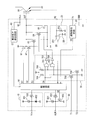
- FIG. 1 is a block diagram showing an example of an intelligent power module (hereinafter referred to as IPM) to which the control device of the present invention is applied.
- IPM intelligent power module
- This IPM is applied to, for example, a voltage source inverter that drives a motor.
- a voltage source inverter that drives a motor.
- FIG. 1 six switching elements Q1 to Q6, six feedback diodes D1 to D6, and Control devices 1 to 6 are provided.
- the switching elements Q1 to Q6 are voltage-controlled switching elements such as IGBTs. Switching elements Q1 and Q4 are connected in series, switching elements Q2 and Q5 are connected in series, and switching elements Q3 and Q6 are connected in series. Each of the switching elements connected in series is connected between a main power terminal P on the positive side and a main power terminal N on the negative side. A common connection portion of the switching elements Q1 and Q4 is connected to the output terminal U. The common connection part of the switching elements Q2 and Q5 is connected to the output terminal V. A common connection portion of the switching elements Q3 and Q6 is connected to the output terminal W.
- Each of the feedback diodes D1 to D6 is connected in parallel to the corresponding switching element Q1 to Q6.
- the control devices 1 to 6 include high-potential side control devices 1 to 3 that respectively perform driving control of the switching elements Q1 to Q3, and low-potential side control devices 4 to 6 that respectively perform drive control of the switching elements Q4 to Q6. Consists of.
- Each of the control devices 1 to 6 includes a power supply voltage terminal Vcc, a reference potential terminal GND, an input terminal Vin, an output terminal OUT, an overcurrent detection terminal OC, and an alarm terminal ALM.
- Each of the power supply voltage terminals Vcc of the control devices 1 to 3 is connected to the corresponding high voltage side power supply voltage terminals VccU, VccV, VccW.
- Each of the reference potential terminals GND of the control devices 1 to 3 is connected to a corresponding high-voltage side reference potential terminal GNDU, GNDV, GNDW, and is connected to a corresponding output terminal U, V, W.
- Each of the input terminals Vin of the control devices 1 to 3 is connected to a corresponding high-voltage side input terminal VinU, VinV, VinW.
- Each of the output terminals OUT of the control devices 1 to 3 is connected to the gates of the corresponding switching elements Q1 to G3.
- Each of the overcurrent detection terminals OC of the control devices 1 to 3 is connected to the current output terminals of the corresponding switching elements Q1 to Q3.
- Each of the alarm terminals ALM of the control devices 1 to 3 is connected to a corresponding high voltage side alarm terminal ALMU, ALMV, ALMW.
- the power supply voltage terminals Vcc of the control devices 4 to 6 are commonly connected, and the common connection portion is connected to the low voltage side power supply voltage terminal Vcc.
- the reference potential terminals GND of the control devices 4 to 6 are commonly connected, and the common connection portion is connected to the main power supply terminal N.
- Each of the input terminals Vin of the control devices 4 to 6 is connected to a corresponding low-voltage side input terminal VinX, VinY, VinZ.
- Each of the output terminals OUT of the control devices 4 to 6 is connected to the gates of the corresponding switching elements Q4 to Q6.
- Each of the overcurrent detection terminals OC of the control devices 4 to 6 is connected to the current output terminals of the corresponding switching elements Q4 to Q6.
- the alarm terminals ALM of the control devices 4 to 6 are commonly connected, and the common connection portion is connected to the low-voltage side alarm terminal ALM.
- the control devices 1 to 6 are provided with test terminals to be described later that are used during a shipping test (test operation). In FIG. 1, the test terminals are omitted. Yes.
- FIG. 2 is a circuit diagram showing a configuration of the first embodiment of the control device of the present invention.
- the control device according to the first embodiment is applied to the IPM control devices 1 to 6 shown in FIG.
- This control device corresponds to, for example, the control device 6 shown in FIG. 1, and drives and controls the switching element Q6 connected to the output terminal OUT as shown in FIG. Therefore, as shown in FIG. 2, the control device includes an input signal receiving circuit 10, an overcurrent detection circuit 20, an overheat detection circuit 30, a potential drop detection circuit 40, a drive circuit 50, and a plurality of transistors 61.
- a transistor operation control unit 70 To 65, a transistor operation control unit 70, and an alarm output circuit 80.
- the control device also includes a power supply voltage terminal Vcc, a reference potential terminal GND, an input terminal Vin, an output terminal OUT, an overcurrent detection terminal OC, an overheat detection terminal TE, an alarm terminal ALM, and test terminals T1 and T2. .
- Each of the plurality of transistors 61 to 65 has the following function according to the drive control of the switching element Q6, and has a withstand voltage of 20 [V] or more.
- the output terminals of the plurality of transistors 61 to 65 are commonly connected to the output terminal OUT.
- the transistor 61 functions as a turn-on transistor that is used when the switching element Q6 connected to the output terminal OUT is turned on during normal switching.
- the transistor 61 is a P-type MOS transistor, and its output current is, for example, 1.5 [A].
- the transistor 62 functions as a soft cutoff transistor that is used to gradually turn off the switching element Q6 when the overcurrent detection circuit 20 detects an overcurrent.
- the transistor 62 is an N-type MOS transistor, and its output current is, for example, 200 [mA].
- the transistor 63 is an off-protection transistor used for lowering the output impedance in order to prevent a malfunction when the switching element Q6 is normally switched on.
- the transistor 63 is an N-type MOS transistor, and its output current is, for example, 1 [A].
- Each of the transistors 64 and 65 has the same function as a turn-off transistor used when the switching element Q6 is turned off during normal switching. This turn-off transistor is divided into a plurality of transistors 64 and 65.
- Each of the output currents of the transistors 64 and 65 is, for example, 1.5 [A]. Therefore, the two transistors 64 and 65 function as a total output current of 3 [A].
- the turn-off transistor may be divided into a plurality of transistors having an ability smaller than the ability (output current) in the case of being constituted by a single transistor.
- the input signal receiving circuit 10 receives an input signal supplied to the input terminal Vin and outputs a signal corresponding to the reception to the driving circuit 50. Therefore, the input signal receiving circuit 10 includes a current source 101, a Zener diode 102, and an inverter 103 with a hysteresis function.
- the overcurrent detection circuit 20 detects whether or not the current flowing through a switching element (not shown) connected to the output terminal OUT is an overcurrent. If an overcurrent is detected, the overcurrent detection signal S5 is used as a drive circuit. Output to 50. For this reason, the overcurrent detection circuit 20 includes a comparator 201 and a resistor 202. A part of the current flowing through the switching element is input to the overcurrent detection terminal OC, and a detection voltage is generated at both ends of the resistor 201 by this input current. The comparator 201 compares the detected voltage with the reference voltage ER, and outputs an overcurrent detection signal S5 to the drive circuit 50 when the detected voltage is equal to or higher than the reference voltage ER.
- the overheat detection circuit 30 detects whether or not a switching element (not shown) connected to the output terminal OUT is in an overheat state, and outputs an overheat detection signal S6 to the drive circuit 50 when the overheat state is detected. To do. For this reason, the overheat detection circuit 30 inputs a detection current of a temperature sensor (not shown) that detects a part of the current flowing through the switching element to the overheat detection terminal TE. Then, based on the detected current, it is determined whether or not the switching element is in an overheated state. If it is determined that the switching element is in an overheated state, an overheat detection signal S6 is output to the drive circuit 50.
- the potential drop detection circuit 40 detects the power supply voltage supplied to the power supply voltage terminal Vcc, and outputs a potential drop signal S7 to the drive circuit 50 when the detected voltage is not more than a predetermined value.
- the drive circuit 50 outputs a drive signal S1 for turning on the switching element Q6 and a drive signal S4 for turning off the switching element Q6 based on the input signal received by the input signal receiving circuit 10. Therefore, when the switching element Q6 is turned on, only the transistor 61 is turned on by the drive signal S1, the power supply voltage Vcc is applied to the gate of the switching element Q6, and the gate is charged. Further, when the switching element Q6 is turned off, only the turn-off transistors 64 and 65 are turned on all at once by the drive signal S4, the gate of the switching element Q6 is connected to the ground, and the gate charge is discharged.
- the drive circuit 50 drives the switching element Q6 gently based on the overcurrent detection signal S5 output from the overcurrent detection circuit 20 or the overheat detection signal S6 output from the overheat detection circuit 30. S2 is output. Therefore, the drive signal S2 turns on the soft cutoff transistor 62, connects the gate of the switching element Q6 to the ground, and gradually discharges the gate charge.
- the drive circuit 50 outputs the drive signal S3 when turning off for protection of the switching element Q6 based on the potential drop signal S7 output from the potential drop detection circuit 40.
- the drive signal S3 turns on the off-protection transistor 63, connects the gate of the switching element Q6 to the ground, and protects the switching element Q6.
- the drive circuit 50 outputs an overcurrent detection signal S5 from the overcurrent detection circuit 20, outputs an overheat detection signal S6 from the overheat detection circuit 30, or receives a potential drop detection signal S7 from the potential drop detection circuit 40.
- the alarm signal S8 is output to the alarm output circuit 80. Further, when the alarm factor is eliminated, the output of the alarm signal S8 is stopped.
- the alarm output circuit 80 outputs the alarm signal S8 to the alarm terminal ALM when the drive circuit 50 outputs the alarm signal S8, and stops the output of the alarm signal S8 when the cause of the alarm is resolved. Therefore, the alarm output circuit 80 includes a current source 801, a transistor 802, and an inverter 803 with a hysteresis function.
- the transistor operation control unit 70 operates the two transistors 64 and 65 having the same function in the normal operation so as to realize the original function, and operates the two transistors 64 and 65 individually in the test operation.
- the output current can be measured with an IC tester.
- the transistor operation control unit 70 controls the two transistors 64 and 65 on or off simultaneously or collectively with the same drive signal S4 output from the drive circuit 50.
- the transistor operation control unit 70 includes NAND circuits (NAND circuits) 701 and 702, an inverter circuit 703, pull-up resistors 705 and 706, and transistors 708 and 709.
- a drive signal S4 output from the drive circuit 50 is input to one of the input terminals of the NAND circuits 701 and 702.
- a power supply voltage is applied to the other input terminal of the NAND circuit 701 through a pull-up resistor 706.
- the other input terminal of the NAND circuit 701 is connected to the ground via the transistor 709.
- a power supply voltage is applied to the other input terminal of the NAND circuit 702 via a pull-up resistor 705.
- the other input terminal of the NAND circuit 702 is connected to the ground via the transistor 708.
- the output terminal of the NAND circuit 701 is connected to the gate of the transistor 64 via the inverter circuit 703.
- the output terminal of the NAND circuit 702 is connected to the gate of the transistor 65 via the inverter circuit 704.
- the NAND circuit 701 and the inverter circuit 703 function as an AND circuit.
- the NAND circuit 702 and the inverter circuit 704 function as an AND circuit.
- Inverter circuits 703 and 704 each function as a buffer circuit.
- the control device having such a configuration is manufactured by a semiconductor wafer process, and a shipping test (operation test) of the control device is performed by probing in the state of a silicon wafer. In the shipping test of this control device, an IC tester is used, and the output current is measured for each of the transistors 61 to 65 in the output stage.
- this control device includes a transistor operation control unit 70.
- the transistor operation control unit 70 has a normal operation and a test operation. The operation in each case will be described.
- a test operation when an H level (high level) signal is applied only to the test terminal T1, the transistor 708 is turned on, so that one input terminal of the NAND circuit 702 becomes L level (low level). .
- the drive signal S4 output from the drive circuit 50 is supplied to the gate of the transistor 64 via the NAND circuit 701 and the inverter 703. Therefore, when the transistor 64 is turned on by the drive signal S4, the output current of the transistor 64 can be measured by the IC tester.
- the transistor 709 is turned on, so that one input terminal of the NAND circuit 701 becomes L level.
- the transistor 708 is off, one input terminal of the NAND circuit 702 becomes H level. Therefore, the drive signal S4 output from the drive circuit 50 is supplied to the gate of the transistor 65 via the NAND circuit 702 and the inverter 704. Therefore, when the transistor 65 is turned on by the drive signal S4, the output current of the transistor 65 can be measured by the IC tester.
- both transistors 708 and 709 are not operated. For this reason, the power supply voltage is applied to one of the input terminals of each of the NAND circuits 701 and 702 via the pull-up resistors 705 and 706, so that one of the input terminals of each of the NAND circuits 701 and 702 is at the H level. Become. Therefore, the drive signal S4 output from the drive circuit 50 is supplied to the gate of the transistor 64 via the NAND circuit 701 and the inverter 703, and is supplied to the gate of the transistor 65 via the NAND circuit 702 and the inverter 704. Is done. Therefore, the transistors 64 and 65 are collectively driven by the same drive signal S4.
- the turn-off transistor for turning off the switching element is divided into two transistors 64 and 65.
- the transistor operation control unit 70 is provided in addition to the configuration. For this reason, according to the first embodiment, during the test operation of the shipping test, the two transistors 64 and 65 are individually operated to use the respective output currents without using the existing IC tester without improving the evaluation board. And can be measured with high accuracy. In the normal operation after shipment, the two transistors 64 and 65 having the same function can perform an operation for realizing the original function.
- FIG. 3 is a circuit diagram showing a configuration of the second embodiment of the control device of the present invention.
- the control device according to the second embodiment is applied to the IPM control devices 1 to 6 shown in FIG.
- This control device corresponds to, for example, the control device 6 shown in FIG. 1, and drives and controls the switching element Q6 connected to the output terminal OUT as shown in FIG.
- the control device includes an input signal receiving circuit 10A, an overcurrent detection circuit 20A, an overheat detection circuit 30, a potential drop detection circuit 40, a drive circuit 50A, and a plurality of transistors 61.
- a transistor operation control unit 70A To 63 and 66 to 68, a transistor operation control unit 70A, an alarm output circuit 80A, and a regulator 90.
- this control device includes a power supply voltage terminal Vcc, a reference potential terminal GND, an input terminal Vin, an output terminal OUT, an overcurrent detection terminal OC, an overheat detection terminal TE, an alarm terminal ALM, a data input terminal DATE, and a clock input terminal CLK. It has.
- a power supply voltage of about 15 [V] is applied to the power supply voltage terminal Vcc, and the plurality of transistors 61 to 63 and 66 to 68 are operated by this power supply voltage.
- the regulator 90 generates a voltage of 5 [V] stabilized by the power supply voltage, and each circuit and each unit operate by the generated voltage.
- Each of the plurality of transistors 61 to 63 and 66 to 68 has the following function according to the drive control of the switching element Q6, and has a withstand voltage of 20 [V] or more.
- the output terminals of the plurality of transistors 61 to 63 and 66 to 68 are commonly connected to the output terminal OUT.
- the transistors 61 to 63 have the same functions as the transistors 61 to 63 in FIG. However, in this example, the output current of the turn-on transistor 61 is 1 [A].
- the output current of the soft cutoff transistor 62 is 400 [mA].
- Each of the transistors 66 to 68 has the same function as a turn-off transistor used for turning off the normal switching of the switching element Q6.
- the turn-off transistor is divided into a plurality of transistors 66 to 68, and each of the output currents of the transistors 66 to 68 is, for example, 1 [A]. Therefore, the three transistors 66 to 68 function as a total output current of 3 [A].
- the input signal receiving circuit 10A receives an input signal supplied to the input terminal Vin, and outputs a signal corresponding to the reception to the drive circuit 50A.
- the input signal receiving circuit 10 includes a current source 101, resistors 104 and 105, a Zener diode 102, and an inverter 103 with a hysteresis function.
- the overcurrent detection circuit 20A detects whether or not the current flowing through the switching element Q6 connected to the output terminal OUT is an overcurrent. If an overcurrent is detected, the overcurrent detection circuit 20A outputs an overcurrent detection signal S5 to the drive circuit 50A. .
- the overcurrent detection circuit 20A includes a comparator 201 and voltage dividing resistors 203 and 204. A part of the current flowing through the switching element Q6 is input to the overcurrent detection terminal OC, and a divided voltage is generated by the voltage dividing resistors 203 and 204 by this input current.
- the comparator 201 compares the divided voltage with the reference voltage ER, and outputs an overcurrent detection signal S5 to the drive circuit 50A when the divided voltage is equal to or higher than the reference voltage ER.
- the overheat detection circuit 30 is configured in the same manner as the overheat detection circuit 30 of FIG. 2, and outputs an overheat detection signal S6 to the drive circuit 50A.
- the potential drop detection circuit 40 is configured in the same manner as the potential drop detection circuit 40 of FIG. 2, and outputs a potential drop signal S7 to the drive circuit 50A.
- the drive circuit 50A outputs a drive signal S1 for turning on the switching element Q6 and a drive signal S4 for turning off the switching element Q6 based on the input signal received by the input signal receiving circuit 10A. Therefore, when the switching element Q6 is turned on, only the transistor 61 is turned on by the drive signal S1, the power supply voltage Vcc is applied to the gate of the switching element Q6, and the gate is charged. When the switching element Q6 is turned off, only the turn-off transistors 66 to 68 are turned on at the same time by the drive signal S4, the gate of the switching element Q6 is connected to the ground, and the gate charge is discharged.
- the drive circuit 50A drives the switching element Q6 gently based on the overcurrent detection signal S5 output from the overcurrent detection circuit 20A or the overheat detection signal S6 output from the overheat detection circuit 30. S2 is output. Therefore, the drive signal S2 turns on the soft cutoff transistor 62, connects the gate of the switching element Q6 to the ground, and gradually discharges the gate charge.
- the drive circuit 50A outputs a drive signal S3 when turning off for protection of the switching element Q6 based on the potential drop signal S7 output from the potential drop detection circuit 40.
- the drive signal S3 turns on the off-protection transistor 63, connects the gate of the switching element Q6 to the ground, and protects the switching element Q6.
- the drive circuit 50A receives the overcurrent detection signal S5 from the overcurrent detection circuit 20A, the overheat detection signal S6 from the overheat detection circuit 30, or the potential drop detection signal S7 from the potential drop detection circuit 40.
- the alarm signal S8 is output to the alarm output circuit 80A. Further, when the alarm factor is eliminated, the output of the alarm signal S8 is stopped.
- the alarm output circuit 80A outputs the alarm signal S8 to the alarm terminal ALM when the drive circuit 50A outputs the alarm signal S8, and stops the output of the alarm signal S8 when the cause of the alarm is resolved. Therefore, the alarm output circuit 80A includes a current source 801, a transistor 802, resistors 804 and 805, a Zener diode 806, and an inverter 803 with a hysteresis function.
- the transistor operation control unit 70A operates the three transistors 66 to 68 having the same function in the normal operation so as to realize the original function, and operates the three transistors 66 to 68 individually in the test operation.
- the output current can be measured with an IC tester.
- the transistor operation control unit 70A controls the three transistors 66 to 68 simultaneously or collectively with the same drive signal S4 output from the drive circuit 50A.
- the transistor operation control unit 70A includes NAND circuits 711 to 713, inverter circuits 714 to 716, pull-up resistors 717 to 719, transistors 720 to 722, and a shift register 730. ing.
- a drive signal S4 output from the drive circuit 50A is input to each of one input terminals of the NAND circuits 711 to 713.
- a power supply voltage is applied to each of the other input terminals of the NAND circuits 711 to 713 via the pull-up resistors 717 to 719.
- the other input terminals of the NAND circuits 711 to 713 are connected to the ground via the transistors 720 to 722, respectively.
- the outputs of the output terminals 740, 750, and 760 of the shift register 730 are input to the gates of the transistors 720 to 722, respectively.
- the shift register 730 sequentially inputs input data with a clock, and outputs the input data in parallel from output terminals 740, 750, and 760. Therefore, the shift register 730 is connected to a data input terminal DATA to which data is input and a clock input terminal CLK to which a clock is input.
- the control device having such a configuration is manufactured by a semiconductor wafer process, and a shipping test (operation test) of the control device is performed by probing in the state of a silicon wafer. An IC tester is used in the shipping test of this control device, and the output current is measured for each of the transistors 61 to 63 and 66 to 68 in the output stage.
- the turn-off transistors 66 to 68 are constituted by one, and when the output current is 3 [A], the above IC tester is used. With this, the output current cannot be measured.
- the turn-off transistor is divided into a plurality of transistors 66 to 68, and each of the output currents of the transistors 66 to 68 is, for example, 1 [A]. Further, this control device includes a transistor operation control unit 70A.
- the transistor operation control unit 70A has a normal operation and a test operation, and the operation in each case will be described.
- the shift register 730 is operated with a clock, test data is sequentially input, and the input data is output from the output terminals 740, 750, and 760, and the gates of the transistors 720 to 722 are input. To supply.
- the transistor 720 When the output terminals 740, 750, and 760 of the shift register 730 are “L”, “H”, and “H”, the transistor 720 is turned off, the transistor 721 is turned on, and the transistor 722 is turned on. .
- the drive signal S4 output from the drive circuit 50A can be supplied to the gate of the transistor 66 via the NAND circuit 711 and the inverter 714. Therefore, when the transistor 66 is turned on by the drive signal S4, the output current of the transistor 66 can be measured by the IC tester.
- the transistor 720 is on, the transistor 721 is off, and the transistor 722 is on Become.
- the drive signal S4 output from the drive circuit 50A can be supplied to the gate of the transistor 67 via the NAND circuit 712 and the inverter 715. Therefore, when the transistor 67 is turned on by the drive signal S4, the output current of the transistor 67 can be measured by the IC tester.
- the transistor 720 is on, the transistor 721 is on, and the transistor 722 is off It becomes.
- the drive signal S4 output from the drive circuit 50A can be supplied to the gate of the transistor 68 via the NAND circuit 713 and the inverter 716. Therefore, when the transistor 68 is turned on by the drive signal S4, the output current of the transistor 68 can be measured by the IC tester.
- the transistors 720 to 722 and the shift register 730 are not operated. Therefore, since the power supply voltage is applied to each of the input terminals of the NAND circuits 711 to 713 via the pull-up resistors 717 to 719, all of the input terminals of the NAND circuits 711 to 713 are at the H level. Clearly, the drive signal S4 output from the drive circuit 50A is supplied to the gate of the transistor 66 via the NAND circuit 711 and the inverter 714, and is supplied to the gate of the transistor 67 via the NAND circuit 712 and the inverter 715. In addition, the signal is supplied to the gate of the transistor 68 via the NAND circuit 713 and the inverter 716. For this reason, the transistors 66 to 68 are collectively driven by the same drive signal S4.
- the turn-off transistor for turning off the switching element is constituted by the three transistors 66-68.
- the transistor operation control unit 70A is provided in addition to the configuration. Therefore, according to the second embodiment, during the test operation of the shipping test, the three transistors 66 to 68 are individually operated to use the output currents and the existing IC tester without improving the evaluation board. And can be measured with high accuracy. In the normal operation after shipment, the three transistors 66 to 68 having the same function can perform an operation for realizing the original function.
- the transistor for turning off the switching element is composed of the plurality of transistors 64 and 65, and the transistor operation control unit 70 is provided accordingly.
- the transistor such as the transistor 61 for turning on the switching element and the transistor 63 for protecting the switching element may be composed of a plurality of transistors.
- a transistor operation control unit similar to the transistor operation control unit 70 is provided between the drive circuit 50 and the plurality of transistors.
- the transistor for turning off the switching element is composed of the plurality of transistors 66 to 68, and the transistor operation control unit 70A is provided in accordance with this.
- the transistor such as the transistor 61 for turning on the switching element and the transistor 63 for protecting the switching element may be composed of a plurality of transistors.
- a transistor operation control unit similar to the transistor operation control unit 70A is provided between the drive circuit 50A and the plurality of transistors.
- the case of the IGBT is described as an example of the switching element.
- the present invention can also be applied to drive control of a power transistor or the like.
- the present invention is applied to a control device for a switching element of a voltage source inverter that drives a motor, for example.
Abstract
The present invention provides a device capable of accurately measuring the output current of a transistor for driving and controlling a switching element, by using an existing IC tester, and without improving an evaluation board. The present invention according to one embodiment is provided with a drive circuit (50), a plurality of transistors (61-65) for driving and controlling a switching element (Q6), and a transistor operation control unit (70). The transistors for turning the switching element (Q6) off are some of the plurality of transistors (64, 65). When operating normally, the transistor operation control unit (70) controls the on/off state of the two transistors (64, 65) simultaneously or en bloc using the same drive signal (S4) outputted from the drive circuit (50). When test-operating, one of the transistors (64, 65) is selected in order, the same drive signal (S4) is supplied to the selected transistor, and the transistors (64, 65) are driven individually.
Description
本発明は、IGBT(Insulated Gate Bipolar Transistor:絶縁ゲート型バイポーラトランジスタ)などの電圧制御型のスイッチング素子を駆動制御する制御装置に関する。
The present invention relates to a control device that drives and controls a voltage-controlled switching element such as an IGBT (Insulated Gate Bipolar Transistor).
この種の制御装置としては、IGBTのターンオンおよびターンオフの駆動を制御するようにしたゲート駆動回路が知られている(特許文献1参照)。この従来装置では、IGBTをターンオンおよびターンオフさせるために第1~第3のMOSトランジスタを備えている。
そして、IGBTをターンオンさせるときには、第1のMOSトランジスタのみをオンさせ、IGBTのゲートに電源電圧を印加する。IGBTをターンオフさせるときには、第1のMOSトランジスタをオフさせ、第2、第3のMOSトランジスタをオンさせ、ターンオフ時の初期には、IGBTのゲート・エミッタ間に溜まった電荷を急速に引き抜くようにしている。 As this type of control device, there is known a gate drive circuit that controls the turn-on and turn-off drive of the IGBT (see Patent Document 1). This conventional device includes first to third MOS transistors for turning on and off the IGBT.
Then, when turning on the IGBT, only the first MOS transistor is turned on, and the power supply voltage is applied to the gate of the IGBT. When the IGBT is turned off, the first MOS transistor is turned off, the second and third MOS transistors are turned on, and the charge accumulated between the gate and the emitter of the IGBT is rapidly extracted at the initial stage of the turn-off. ing.
また、従来の他の制御装置としては、IGBTのターンオンおよびターンオフの駆動制御に加えて、IGBTに流れる電流を検出し、過電流を検出したときにIGBTをオフにしてIGBTを保護するものが知られている。
そして、その従来装置では、IGBTをターンオンさせるターンオン用のトランジスタ、IGBTをターンオフさせるターンオフ用のトランジスタ、およびIGBTを過電流から保護する過電流保護用のトランジスタなど、機能別に複数のトランジスタを備えている。 As another conventional control device, in addition to IGBT turn-on and turn-off drive control, a current that flows through the IGBT is detected, and when an overcurrent is detected, the IGBT is turned off to protect the IGBT. It has been.
The conventional device includes a plurality of transistors according to function, such as a turn-on transistor for turning on the IGBT, a turn-off transistor for turning off the IGBT, and an overcurrent protection transistor for protecting the IGBT from overcurrent. .
しかし、ターンオンおよびターンオフ用のトランジスタは、IGBTをPWM信号でオンオフさせるので、大きな出力電流が必要になる。例えば、IGBTの定格電流が300〔A〕を越えるような場合には、ターンオンおよびターンオフ用のトランジスタの出力電流は2〔A〕を越える場合がある。また、IGBTを駆動制御するためには、ターンオンおよびターンオフ用のトランジスタは、20〔V〕以上の耐圧が必要な場合がある。
However, since the turn-on and turn-off transistors turn on and off the IGBT with a PWM signal, a large output current is required. For example, when the rated current of the IGBT exceeds 300 [A], the output current of the turn-on and turn-off transistors may exceed 2 [A]. In order to drive and control the IGBT, the turn-on and turn-off transistors may require a breakdown voltage of 20 [V] or more.
上記のように、IGBT等のスイッチング素子(パワーデバイス)は、定格電流が数Aから数百Aまであってその幅が広く、定格電流が大きくなるとパワーデバイスの素子面積が大きくなる。素子面積が大きくなると、パワーデバイスを駆動制御する制御装置の制御トランジスタ(出力段トランジスタ)に求められる駆動能力が大きくなり、数〔A〕以上の出力電流が必要な場合がある。
As described above, a switching element (power device) such as an IGBT has a rated current ranging from several A to several hundred A and is wide, and the element area of the power device increases as the rated current increases. As the element area increases, the drive capability required for the control transistor (output stage transistor) of the control device that drives and controls the power device increases, and an output current of several [A] or more may be required.
近年、パワーデバイスの定格電流に対する大電流化が要求され、これに伴い制御回路の出力電流も大きくなってきている。しかし、出荷に先だって、制御装置の出力電流を試験するICテスタの測定電流の上限値の対応は遅れており、2〔A〕程度が上限値となっている。
ICテスタで上限値以上の電流を測定するには、大電流測定用の抵抗の取り付けなど評価ボードの工夫が必要になるが、大電流測定用の抵抗を使用すると測定精度が低下するという課題がある。 In recent years, there has been a demand for an increase in current with respect to the rated current of power devices, and the output current of control circuits has increased accordingly. However, prior to shipment, the correspondence of the upper limit value of the measured current of the IC tester that tests the output current of the control device is delayed, and the upper limit value is about 2 [A].
In order to measure the current exceeding the upper limit with an IC tester, it is necessary to devise an evaluation board such as mounting a resistor for measuring a large current. However, if a resistor for measuring a large current is used, there is a problem that the measurement accuracy decreases. is there.
大電流測定用の抵抗の取り付けた評価ボードでは、制御装置の出力電流が小さい場合には、測定精度の低下が顕著となる。また、大電流測定用の抵抗を取り付けた評価ボードと取り付けない評価ボードを使い分けるようにしてもよい。しかし、この場合には、2つの評価ボードが必要になり試験に要するコストが増加するという課題がある。
そこで、本発明の目的は、上記の課題に着目してなされたものであり、スイッチング素子を駆動制御するトランジスタの出力電流の測定を、評価ボードを改良することなく、既存のICテスタを使用して精度良く測定することが可能な制御装置を提供することにある。 In the evaluation board to which a resistor for measuring a large current is attached, when the output current of the control device is small, the measurement accuracy is remarkably lowered. Also, an evaluation board with a large current measurement resistor attached and an evaluation board without a resistor attached may be used properly. However, in this case, there is a problem that two evaluation boards are required and the cost required for the test increases.
Therefore, the object of the present invention is to pay attention to the above-mentioned problem, and the measurement of the output current of the transistor for driving and controlling the switching element can be performed by using an existing IC tester without improving the evaluation board. It is another object of the present invention to provide a control device that can measure with high accuracy.
本発明の一態様は、電圧制御型のスイッチング素子を駆動制御する制御装置であって、入力信号に応じた駆動信号を生成して出力する駆動回路と、前記駆動回路から出力される駆動信号で駆動され、前記スイッチング素子を駆動制御するトランジスタと、を備え、前記トランジスタは複数のトランジスタからなり、前記複数のトランジスタの動作を制御するトランジスタ動作制御部を備え、前記トランジスタ動作制御部は、通常動作のときには、前記複数のトランジスタに前記駆動回路から出力される同一の駆動信号を供給して一括動作させ、試験動作のときには、前記複数のトランジスタのうちの1つを順に選択し、当該選択されたトランジスタに前記同一の駆動信号を供給して個別に動作させる。
One embodiment of the present invention is a control device that drives and controls a voltage-controlled switching element, and includes a drive circuit that generates and outputs a drive signal according to an input signal, and a drive signal output from the drive circuit. And a transistor that drives and controls the switching element. The transistor includes a plurality of transistors, and includes a transistor operation control unit that controls operations of the plurality of transistors, and the transistor operation control unit operates normally. In this case, the plurality of transistors are supplied with the same drive signal output from the drive circuit to be collectively operated, and in the test operation, one of the plurality of transistors is sequentially selected and the selected transistor is selected. The same drive signal is supplied to the transistors to operate them individually.
本発明の他の態様では、さらに、前記入力信号が入力される入力端子と、前記複数のトランジスタの各出力部が共通に接続される出力端子と、電源電圧が供給される電源端子と、基準電圧となる基準電圧端子とを備えても良い。
本発明の他の態様では、前記トランジスタは、耐圧が20V以上であり、前記スイッチング素子のゲートの充電および放電のうちのいずれか一方を行うようになっているものでも良い。 In another aspect of the present invention, an input terminal to which the input signal is input, an output terminal to which output parts of the plurality of transistors are connected in common, a power supply terminal to which a power supply voltage is supplied, and a reference You may provide the reference voltage terminal used as voltage.
In another aspect of the present invention, the transistor may have a withstand voltage of 20 V or more and perform one of charging and discharging of the gate of the switching element.
本発明の他の態様では、前記トランジスタは、前記スイッチング素子をターンオンさせる複数の第1トランジスタと、前記スイッチング素子をターンオフさせる複数の第2トランジスタとからなり、前記トランジスタ動作制御部は、通常動作のときには、前記複数の第1トランジスタに前記駆動回路から出力される第1駆動信号を供給して一括動作させ、前記複数の第2トランジスタに前記駆動回路から出力される第2駆動信号を供給して一括動作させ、試験動作のときには、前記複数の第1トランジスタのうちの1つを順に選択し、当該選択された第1トランジスタに前記第1駆動信号を供給して個別に動作させ、前記複数の第2トランジスタのうちの1つを順に選択し、当該選択された第2トランジスタに前記第2駆動信号を供給して個別に動作させても良い。
In another aspect of the invention, the transistor includes a plurality of first transistors for turning on the switching element and a plurality of second transistors for turning off the switching element, and the transistor operation control unit is configured to perform normal operation. Sometimes, the first drive signals output from the drive circuit are supplied to the plurality of first transistors to collectively operate, and the second drive signals output from the drive circuit are supplied to the plurality of second transistors. In a test operation, one of the plurality of first transistors is sequentially selected, the first drive signal is supplied to the selected first transistor, and the plurality of first transistors are individually operated. Select one of the second transistors in order, and supply the second drive signal to the selected second transistor. It may be separately operated.
本発明の他の態様では、前記トランジスタは、前記スイッチング素子の駆動制御の内容に応じた動作をする機能別の複数のトランジスタからなり、前記機能別の複数のトランジスタのうちの少なくとも1つは、同一機能を有する複数のトランジスタからなるようにしても良い。
本発明の他の態様では、前記トランジスタ動作制御部は、前記駆動回路と前記複数のトランジスタとの間に設けたゲート回路を備え、前記ゲート回路は、通常動作のときには、前記駆動回路から出力される駆動信号を前記複数のトランジスタのゲートのいずれにも供給し、試験動作のときには、外部からの試験信号に応じて前記駆動信号を前記複数のトランジスタのゲートへ選択的に供給しても良い。 In another aspect of the present invention, the transistor includes a plurality of transistors according to function that operate according to the content of drive control of the switching element, and at least one of the plurality of transistors according to function includes: You may make it consist of several transistors which have the same function.
In another aspect of the present invention, the transistor operation control unit includes a gate circuit provided between the drive circuit and the plurality of transistors, and the gate circuit is output from the drive circuit during normal operation. The drive signal may be supplied to any one of the gates of the plurality of transistors, and during the test operation, the drive signal may be selectively supplied to the gates of the plurality of transistors in accordance with an external test signal.
本発明の他の態様では、前記トランジスタ動作制御部は、前記駆動回路と前記複数のトランジスタとの間に設けたゲート回路と、入力データを直列入力し並列変換して出力するシフトレジスタと、を備え、前記ゲート回路は、通常動作のときには、前記駆動回路から出力される駆動信号を前記複数のトランジスタのゲートのいずれにも供給し、試験動作のときには、前記シフトレジスタから出力されるデータに応じて前記駆動信号を前記複数のトランジスタのゲートへ選択的に供給しても良い。
In another aspect of the present invention, the transistor operation control unit includes a gate circuit provided between the drive circuit and the plurality of transistors, and a shift register that inputs input data in series, converts the input data in parallel, and outputs the converted data. The gate circuit supplies a drive signal output from the drive circuit to any one of the gates of the plurality of transistors during a normal operation, and according to data output from the shift register during a test operation. The drive signal may be selectively supplied to the gates of the plurality of transistors.
本発明の他の態様では、さらに、前記スイッチング素子に流れる電流の一部を入力し、当該入力電流に基づいて前記スイッチング素子に流れる電流が過電流か否かを検出し、過電流を検出した場合には過電流検出信号を前記駆動回路に出力する過電流検出回路と、前記スイッチング素子に流れる電流の一部を検出する温度センサの検出電流を入力し、当該入力した検出電流に基づいて前記スイッチング素子が過熱状態にあるか否かを判定し、過熱状態にあると判定した場合には過熱検出信号を前記駆動回路に出力する過熱検出回路と、電源端子に供給される電源電圧を検出し、当該検出電圧が所定値以下の場合には電源電圧異常信号を前記駆動回路に出力する電源電圧検出回路とを、備えても良い。
In another aspect of the present invention, a part of the current flowing through the switching element is further input, and it is detected whether the current flowing through the switching element is an overcurrent based on the input current, and the overcurrent is detected. In this case, an overcurrent detection circuit that outputs an overcurrent detection signal to the drive circuit and a detection current of a temperature sensor that detects a part of the current flowing through the switching element are input, and the detection current is input based on the input detection current. It is determined whether or not the switching element is in an overheat state. If it is determined that the switching element is in an overheat state, an overheat detection circuit that outputs an overheat detection signal to the drive circuit and a power supply voltage supplied to the power supply terminal are detected. A power supply voltage detection circuit that outputs a power supply voltage abnormality signal to the drive circuit when the detected voltage is a predetermined value or less may be provided.
本発明の他の態様では、さらにアラーム端子を備え、前記駆動回路は、前記過電流検出回路から過電流検出信号が出力され、前記過熱検出回路から過熱検出信号が出力され、または前記電位低下検出回路から電位低下検出信号が出力され場合には、アラーム信号を前記アラーム端子に出力し、アラーム要因が解消された場合には前記アラーム信号の出力を停止するようにしても良い。
In another aspect of the present invention, an alarm terminal is further provided, and the drive circuit outputs an overcurrent detection signal from the overcurrent detection circuit, outputs an overheat detection signal from the overheat detection circuit, or detects the potential drop. When a potential drop detection signal is output from the circuit, an alarm signal may be output to the alarm terminal, and when the cause of the alarm is resolved, the output of the alarm signal may be stopped.
本発明によれば、スイッチング素子を駆動制御するトランジスタの出力電流の測定を、評価ボードを改良することなく、既存のICテスタを使用して精度良く測定することが可能となる。
According to the present invention, it is possible to accurately measure the output current of the transistor that drives and controls the switching element by using an existing IC tester without improving the evaluation board.
以下、本発明の実施の形態を図面に基づいて説明する。
図1は本発明の制御装置が適用されるインテリジェントパワーモジュール(以下、IPMと称する)の一例を示すブロック図である。
〔IPMの構成〕
このIPMは、例えばモータを駆動する電圧形インバータに適用されるものであり、図1に示すように、6個のスイッチング素子Q1~Q6と、6個の帰還ダイオードD1~D6と、本発明に係る制御装置1~6と、を備えている。 Hereinafter, embodiments of the present invention will be described with reference to the drawings.
FIG. 1 is a block diagram showing an example of an intelligent power module (hereinafter referred to as IPM) to which the control device of the present invention is applied.
[Configuration of IPM]
This IPM is applied to, for example, a voltage source inverter that drives a motor. As shown in FIG. 1, six switching elements Q1 to Q6, six feedback diodes D1 to D6, andControl devices 1 to 6 are provided.
図1は本発明の制御装置が適用されるインテリジェントパワーモジュール(以下、IPMと称する)の一例を示すブロック図である。
〔IPMの構成〕
このIPMは、例えばモータを駆動する電圧形インバータに適用されるものであり、図1に示すように、6個のスイッチング素子Q1~Q6と、6個の帰還ダイオードD1~D6と、本発明に係る制御装置1~6と、を備えている。 Hereinafter, embodiments of the present invention will be described with reference to the drawings.
FIG. 1 is a block diagram showing an example of an intelligent power module (hereinafter referred to as IPM) to which the control device of the present invention is applied.
[Configuration of IPM]
This IPM is applied to, for example, a voltage source inverter that drives a motor. As shown in FIG. 1, six switching elements Q1 to Q6, six feedback diodes D1 to D6, and
スイッチング素子Q1~Q6は、IGBTのような電圧制御型のスイッチング素子からなる。スイッチング素子Q1、Q4は直列接続され、スイッチング素子Q2、Q5は直列接続され、スイッチング素子Q3、Q6は直列接続されている。そして、この直列接続されたスイッチング素子のそれぞれは、プラス側の主電源端子Pとマイナス側の主電源端子Nとの間に接続されている。スイッチング素子Q1、Q4の共通接続部は、出力端子Uに接続されている。スイッチング素子Q2、Q5の共通接続部は、出力端子Vに接続されている。スイッチング素子Q3、Q6の共通接続部は、出力端子Wに接続されている。
The switching elements Q1 to Q6 are voltage-controlled switching elements such as IGBTs. Switching elements Q1 and Q4 are connected in series, switching elements Q2 and Q5 are connected in series, and switching elements Q3 and Q6 are connected in series. Each of the switching elements connected in series is connected between a main power terminal P on the positive side and a main power terminal N on the negative side. A common connection portion of the switching elements Q1 and Q4 is connected to the output terminal U. The common connection part of the switching elements Q2 and Q5 is connected to the output terminal V. A common connection portion of the switching elements Q3 and Q6 is connected to the output terminal W.
帰還ダイオードD1~D6のそれぞれは、対応するスイッチング素子Q1~Q6に並列に接続されている。
制御装置1~6は、スイッチング素子Q1~Q3の駆動制御をそれぞれ行う高電位側の制御装置1~3と、スイッチング素子Q4~Q6の駆動制御をそれぞれ行う低電位側の制御装置4~6とからなる。制御装置1~6のそれぞれは、電源電圧端子Vcc、基準電位端子GND、入力端子Vin、出力端子OUT、過電流検出端子OC、およびアラーム端子ALMを備えている。 Each of the feedback diodes D1 to D6 is connected in parallel to the corresponding switching element Q1 to Q6.
Thecontrol devices 1 to 6 include high-potential side control devices 1 to 3 that respectively perform driving control of the switching elements Q1 to Q3, and low-potential side control devices 4 to 6 that respectively perform drive control of the switching elements Q4 to Q6. Consists of. Each of the control devices 1 to 6 includes a power supply voltage terminal Vcc, a reference potential terminal GND, an input terminal Vin, an output terminal OUT, an overcurrent detection terminal OC, and an alarm terminal ALM.
制御装置1~6は、スイッチング素子Q1~Q3の駆動制御をそれぞれ行う高電位側の制御装置1~3と、スイッチング素子Q4~Q6の駆動制御をそれぞれ行う低電位側の制御装置4~6とからなる。制御装置1~6のそれぞれは、電源電圧端子Vcc、基準電位端子GND、入力端子Vin、出力端子OUT、過電流検出端子OC、およびアラーム端子ALMを備えている。 Each of the feedback diodes D1 to D6 is connected in parallel to the corresponding switching element Q1 to Q6.
The
制御装置1~3の電源電圧端子Vccのそれぞれは、対応する高圧側電源電圧端子VccU、VccV、VccWに接続されている。制御装置1~3の基準電位端子GNDのそれぞれは、対応する高圧側基準電位端子GNDU、GNDV、GNDWに接続されるとともに、対応する出力端子U、V、Wに接続されている。制御装置1~3の入力端子Vinのそれぞれは、対応する高圧側入力端子VinU、VinV、VinWに接続されている。制御装置1~3の出力端子OUTのそれぞれは、対応するスイッチング素子Q1~G3のゲートに接続されている。制御装置1~3の過電流検出端子OCのそれぞれは、対応するスイッチング素子Q1~Q3の電流出力端子に接続されている。制御装置1~3のアラーム端子ALMのそれぞれは、対応する高圧側アラーム端子ALMU、ALMV、ALMWに接続されている。
Each of the power supply voltage terminals Vcc of the control devices 1 to 3 is connected to the corresponding high voltage side power supply voltage terminals VccU, VccV, VccW. Each of the reference potential terminals GND of the control devices 1 to 3 is connected to a corresponding high-voltage side reference potential terminal GNDU, GNDV, GNDW, and is connected to a corresponding output terminal U, V, W. Each of the input terminals Vin of the control devices 1 to 3 is connected to a corresponding high-voltage side input terminal VinU, VinV, VinW. Each of the output terminals OUT of the control devices 1 to 3 is connected to the gates of the corresponding switching elements Q1 to G3. Each of the overcurrent detection terminals OC of the control devices 1 to 3 is connected to the current output terminals of the corresponding switching elements Q1 to Q3. Each of the alarm terminals ALM of the control devices 1 to 3 is connected to a corresponding high voltage side alarm terminal ALMU, ALMV, ALMW.
制御装置4~6の電源電圧端子Vccは共通接続され、共通接続部が低圧側電源電圧端子Vccに接続されている。制御装置4~6の基準電位端子GNDは共通接続され、共通接続部が主電源端子Nに接続されている。制御装置4~6の入力端子Vinのそれぞれは、対応する低圧側入力端子VinX、VinY、VinZに接続されている。制御装置4~6の出力端子OUTのそれぞれは、対応するスイッチング素子Q4~Q6のゲートに接続されている。制御装置4~6の過電流検出端子OCのそれぞれは、対応するスイッチング素子Q4~Q6の電流出力端子に接続されている。制御装置4~6のアラーム端子ALMは共通接続され、共通接続部が低圧側アラーム端子ALMに接続されている。
ここで、制御装置1~6は、上記の各端子の他に出荷試験(試験動作)のときに使用する後述の試験用の端子を備えるが、図1ではその試験用の端子は省略されている。 The power supply voltage terminals Vcc of the control devices 4 to 6 are commonly connected, and the common connection portion is connected to the low voltage side power supply voltage terminal Vcc. The reference potential terminals GND of the control devices 4 to 6 are commonly connected, and the common connection portion is connected to the main power supply terminal N. Each of the input terminals Vin of the control devices 4 to 6 is connected to a corresponding low-voltage side input terminal VinX, VinY, VinZ. Each of the output terminals OUT of the control devices 4 to 6 is connected to the gates of the corresponding switching elements Q4 to Q6. Each of the overcurrent detection terminals OC of the control devices 4 to 6 is connected to the current output terminals of the corresponding switching elements Q4 to Q6. The alarm terminals ALM of the control devices 4 to 6 are commonly connected, and the common connection portion is connected to the low-voltage side alarm terminal ALM.
Here, in addition to the above terminals, thecontrol devices 1 to 6 are provided with test terminals to be described later that are used during a shipping test (test operation). In FIG. 1, the test terminals are omitted. Yes.
ここで、制御装置1~6は、上記の各端子の他に出荷試験(試験動作)のときに使用する後述の試験用の端子を備えるが、図1ではその試験用の端子は省略されている。 The power supply voltage terminals Vcc of the control devices 4 to 6 are commonly connected, and the common connection portion is connected to the low voltage side power supply voltage terminal Vcc. The reference potential terminals GND of the control devices 4 to 6 are commonly connected, and the common connection portion is connected to the main power supply terminal N. Each of the input terminals Vin of the control devices 4 to 6 is connected to a corresponding low-voltage side input terminal VinX, VinY, VinZ. Each of the output terminals OUT of the control devices 4 to 6 is connected to the gates of the corresponding switching elements Q4 to Q6. Each of the overcurrent detection terminals OC of the control devices 4 to 6 is connected to the current output terminals of the corresponding switching elements Q4 to Q6. The alarm terminals ALM of the control devices 4 to 6 are commonly connected, and the common connection portion is connected to the low-voltage side alarm terminal ALM.
Here, in addition to the above terminals, the
〔制御装置の第1実施形態〕
図2は、本発明の制御装置の第1実施形態の構成を示す回路図である。
第1実施形態に係る制御装置は、図1に示すIPMの制御装置1~6に適用されるものである。
この制御装置は、例えば図1に示す制御装置6に相当し、図2に示すように、出力端子OUTに接続されるスイッチング素子Q6を駆動制御する。
このため、制御装置は、図2に示すように、入力信号受信回路10と、過電流検出回路20と、過熱検出回路30と、電位低下検出回路40と、駆動回路50と、複数のトランジスタ61~65と、トランジスタ動作制御部70と、アラーム出力回路80とを備えている。 [First Embodiment of Control Device]
FIG. 2 is a circuit diagram showing a configuration of the first embodiment of the control device of the present invention.
The control device according to the first embodiment is applied to theIPM control devices 1 to 6 shown in FIG.
This control device corresponds to, for example, thecontrol device 6 shown in FIG. 1, and drives and controls the switching element Q6 connected to the output terminal OUT as shown in FIG.
Therefore, as shown in FIG. 2, the control device includes an inputsignal receiving circuit 10, an overcurrent detection circuit 20, an overheat detection circuit 30, a potential drop detection circuit 40, a drive circuit 50, and a plurality of transistors 61. To 65, a transistor operation control unit 70, and an alarm output circuit 80.
図2は、本発明の制御装置の第1実施形態の構成を示す回路図である。
第1実施形態に係る制御装置は、図1に示すIPMの制御装置1~6に適用されるものである。
この制御装置は、例えば図1に示す制御装置6に相当し、図2に示すように、出力端子OUTに接続されるスイッチング素子Q6を駆動制御する。
このため、制御装置は、図2に示すように、入力信号受信回路10と、過電流検出回路20と、過熱検出回路30と、電位低下検出回路40と、駆動回路50と、複数のトランジスタ61~65と、トランジスタ動作制御部70と、アラーム出力回路80とを備えている。 [First Embodiment of Control Device]
FIG. 2 is a circuit diagram showing a configuration of the first embodiment of the control device of the present invention.
The control device according to the first embodiment is applied to the
This control device corresponds to, for example, the
Therefore, as shown in FIG. 2, the control device includes an input
また、この制御装置は、電源電圧端子Vcc、基準電位端子GND、入力端子Vin、出力端子OUT、過電流検出端子OC、過熱検出端子TE、アラーム端子ALM、および試験端子T1、T2を備えている。
複数のトランジスタ61~65のそれぞれは、スイッチング素子Q6の駆動制御に応じて以下の機能を有し、かつ、耐圧電圧が20〔V〕以上のものが使用される。また、複数のトランジスタ61~65の各出力端子は、出力端子OUTに共通接続されている。 The control device also includes a power supply voltage terminal Vcc, a reference potential terminal GND, an input terminal Vin, an output terminal OUT, an overcurrent detection terminal OC, an overheat detection terminal TE, an alarm terminal ALM, and test terminals T1 and T2. .
Each of the plurality oftransistors 61 to 65 has the following function according to the drive control of the switching element Q6, and has a withstand voltage of 20 [V] or more. The output terminals of the plurality of transistors 61 to 65 are commonly connected to the output terminal OUT.
複数のトランジスタ61~65のそれぞれは、スイッチング素子Q6の駆動制御に応じて以下の機能を有し、かつ、耐圧電圧が20〔V〕以上のものが使用される。また、複数のトランジスタ61~65の各出力端子は、出力端子OUTに共通接続されている。 The control device also includes a power supply voltage terminal Vcc, a reference potential terminal GND, an input terminal Vin, an output terminal OUT, an overcurrent detection terminal OC, an overheat detection terminal TE, an alarm terminal ALM, and test terminals T1 and T2. .
Each of the plurality of
トランジスタ61は、出力端子OUTに接続されるスイッチング素子Q6の通常のスイッチングのターンオン時に使用されるターンオン用のトランジスタとして機能する。トランジスタ61は、P型のMOSトランジスタからなり、その出力電流は例えば1.5〔A〕である。
トランジスタ62は、過電流検出回路20が過電流を検出したときにスイッチング素子Q6を徐々にオフにさせるために使用されるソフト遮断用のトランジスタとして機能する。このトランジスタ62は、N型のMOSトランジスタからなり、その出力電流は例えば200〔mA〕である。 Thetransistor 61 functions as a turn-on transistor that is used when the switching element Q6 connected to the output terminal OUT is turned on during normal switching. The transistor 61 is a P-type MOS transistor, and its output current is, for example, 1.5 [A].
Thetransistor 62 functions as a soft cutoff transistor that is used to gradually turn off the switching element Q6 when the overcurrent detection circuit 20 detects an overcurrent. The transistor 62 is an N-type MOS transistor, and its output current is, for example, 200 [mA].
トランジスタ62は、過電流検出回路20が過電流を検出したときにスイッチング素子Q6を徐々にオフにさせるために使用されるソフト遮断用のトランジスタとして機能する。このトランジスタ62は、N型のMOSトランジスタからなり、その出力電流は例えば200〔mA〕である。 The
The
トランジスタ63は、スイッチング素子Q6の通常のスイッチングオン時の誤動作を防止するために出力インピーダンスを低下させるために使用されるオフ保護用のトランジスタである。このトランジスタ63はN型のMOSトランジスタからなり、その出力電流は例えば1〔A〕である。
トランジスタ64、65のそれぞれは、スイッチング素子Q6の通常のスイッチングのターンオフ時に使用されるターンオフ用のトランジスタとして同一の機能を有する。このターンオフ用のトランジスタは、分割して複数のトランジスタ64、65で構成するようにした。トランジスタ64、65の出力電流のそれぞれは、例えば1.5〔A〕からなる。このため、2つのトランジスタ64、65は、全体で出力電流が3〔A〕のものとして機能する。 Thetransistor 63 is an off-protection transistor used for lowering the output impedance in order to prevent a malfunction when the switching element Q6 is normally switched on. The transistor 63 is an N-type MOS transistor, and its output current is, for example, 1 [A].
Each of the transistors 64 and 65 has the same function as a turn-off transistor used when the switching element Q6 is turned off during normal switching. This turn-off transistor is divided into a plurality of transistors 64 and 65. Each of the output currents of the transistors 64 and 65 is, for example, 1.5 [A]. Therefore, the two transistors 64 and 65 function as a total output current of 3 [A].
トランジスタ64、65のそれぞれは、スイッチング素子Q6の通常のスイッチングのターンオフ時に使用されるターンオフ用のトランジスタとして同一の機能を有する。このターンオフ用のトランジスタは、分割して複数のトランジスタ64、65で構成するようにした。トランジスタ64、65の出力電流のそれぞれは、例えば1.5〔A〕からなる。このため、2つのトランジスタ64、65は、全体で出力電流が3〔A〕のものとして機能する。 The
Each of the
ここで、ターンオフ用のトランジスタは、単一のトランジスタで構成する場合の能力(出力電流)よりも小さな能力の複数のトランジスタに分割すれば良い。
次に、この制御装置の各回路について具体的に説明する。
入力信号受信回路10は、入力端子Vinに供給される入力信号を受信し、この受信に応じた信号を駆動回路50に出力する。このため、入力信号受信回路10は、電流源101、ツェナダイオード102、およびヒステシス機能付きのインバータ103から構成される。 Here, the turn-off transistor may be divided into a plurality of transistors having an ability smaller than the ability (output current) in the case of being constituted by a single transistor.
Next, each circuit of this control device will be specifically described.
The inputsignal receiving circuit 10 receives an input signal supplied to the input terminal Vin and outputs a signal corresponding to the reception to the driving circuit 50. Therefore, the input signal receiving circuit 10 includes a current source 101, a Zener diode 102, and an inverter 103 with a hysteresis function.
次に、この制御装置の各回路について具体的に説明する。
入力信号受信回路10は、入力端子Vinに供給される入力信号を受信し、この受信に応じた信号を駆動回路50に出力する。このため、入力信号受信回路10は、電流源101、ツェナダイオード102、およびヒステシス機能付きのインバータ103から構成される。 Here, the turn-off transistor may be divided into a plurality of transistors having an ability smaller than the ability (output current) in the case of being constituted by a single transistor.
Next, each circuit of this control device will be specifically described.
The input
過電流検出回路20は、出力端子OUTに接続されるスイッチング素子(図示せず)に流れる電流が過電流か否かを検出し、過電流を検出した場合には過電流検出信号S5を駆動回路50に出力する。
このため、過電流検出回路20は、コンパレータ201と、抵抗202とを備えている。そして、そのスイッチング素子に流れる電流の一部を過電流検出端子OCに入力し、この入力電流により抵抗201の両端に検出電圧を発生させる。コンパレータ201は、その検出電圧を基準電圧ERと比較し、検出電圧が基準電圧ER以上のときに、過電流検出信号S5を駆動回路50に出力する。 Theovercurrent detection circuit 20 detects whether or not the current flowing through a switching element (not shown) connected to the output terminal OUT is an overcurrent. If an overcurrent is detected, the overcurrent detection signal S5 is used as a drive circuit. Output to 50.
For this reason, theovercurrent detection circuit 20 includes a comparator 201 and a resistor 202. A part of the current flowing through the switching element is input to the overcurrent detection terminal OC, and a detection voltage is generated at both ends of the resistor 201 by this input current. The comparator 201 compares the detected voltage with the reference voltage ER, and outputs an overcurrent detection signal S5 to the drive circuit 50 when the detected voltage is equal to or higher than the reference voltage ER.
このため、過電流検出回路20は、コンパレータ201と、抵抗202とを備えている。そして、そのスイッチング素子に流れる電流の一部を過電流検出端子OCに入力し、この入力電流により抵抗201の両端に検出電圧を発生させる。コンパレータ201は、その検出電圧を基準電圧ERと比較し、検出電圧が基準電圧ER以上のときに、過電流検出信号S5を駆動回路50に出力する。 The
For this reason, the
過熱検出回路30は、出力端子OUTに接続されるスイッチング素子(図示せず)が過熱状態にあるか否かを検出し、過熱状態を検出した場合には過熱検出信号S6を駆動回路50に出力する。
このため、過熱検出回路30は、そのスイッチング素子に流れる電流の一部を検出する温度センサ(図示せず)の検出電流を過熱検出端子TEに入力する。そして、その検出電流に基づいてスイッチング素子が過熱状態であるか否かを判定し、過熱状態であると判定した場合には過熱検出信号S6を駆動回路50に出力する。 Theoverheat detection circuit 30 detects whether or not a switching element (not shown) connected to the output terminal OUT is in an overheat state, and outputs an overheat detection signal S6 to the drive circuit 50 when the overheat state is detected. To do.
For this reason, theoverheat detection circuit 30 inputs a detection current of a temperature sensor (not shown) that detects a part of the current flowing through the switching element to the overheat detection terminal TE. Then, based on the detected current, it is determined whether or not the switching element is in an overheated state. If it is determined that the switching element is in an overheated state, an overheat detection signal S6 is output to the drive circuit 50.
このため、過熱検出回路30は、そのスイッチング素子に流れる電流の一部を検出する温度センサ(図示せず)の検出電流を過熱検出端子TEに入力する。そして、その検出電流に基づいてスイッチング素子が過熱状態であるか否かを判定し、過熱状態であると判定した場合には過熱検出信号S6を駆動回路50に出力する。 The
For this reason, the
電位低下検出回路40は、電源電圧端子Vccに供給される電源電圧を検出し、この検出電圧が所定値以下の場合には電位低下信号S7を駆動回路50に出力する。
駆動回路50は、入力信号受信回路10が受信した入力信号に基づき、スイッチング素子Q6をターンオンさせる駆動信号S1と、スイッチング素子Q6をターンオフさせる駆動信号S4を出力する。このため、スイッチング素子Q6のターンオン時には、駆動信号S1によりトンジスタ61のみがオンされ、電源電圧Vccがスイッチング素子Q6のゲートに印加され、ゲートが充電される。また、スイッチング素子Q6のターンオフ時には、駆動信号S4によりターンオフ用トランジスタ64、65のみが一括してオンされ、スイッチング素子Q6のゲートをグランドに接続させて、ゲートの電荷が放電される。 The potentialdrop detection circuit 40 detects the power supply voltage supplied to the power supply voltage terminal Vcc, and outputs a potential drop signal S7 to the drive circuit 50 when the detected voltage is not more than a predetermined value.
Thedrive circuit 50 outputs a drive signal S1 for turning on the switching element Q6 and a drive signal S4 for turning off the switching element Q6 based on the input signal received by the input signal receiving circuit 10. Therefore, when the switching element Q6 is turned on, only the transistor 61 is turned on by the drive signal S1, the power supply voltage Vcc is applied to the gate of the switching element Q6, and the gate is charged. Further, when the switching element Q6 is turned off, only the turn- off transistors 64 and 65 are turned on all at once by the drive signal S4, the gate of the switching element Q6 is connected to the ground, and the gate charge is discharged.
駆動回路50は、入力信号受信回路10が受信した入力信号に基づき、スイッチング素子Q6をターンオンさせる駆動信号S1と、スイッチング素子Q6をターンオフさせる駆動信号S4を出力する。このため、スイッチング素子Q6のターンオン時には、駆動信号S1によりトンジスタ61のみがオンされ、電源電圧Vccがスイッチング素子Q6のゲートに印加され、ゲートが充電される。また、スイッチング素子Q6のターンオフ時には、駆動信号S4によりターンオフ用トランジスタ64、65のみが一括してオンされ、スイッチング素子Q6のゲートをグランドに接続させて、ゲートの電荷が放電される。 The potential
The
また、駆動回路50は、過電流検出回路20から出力される過電流検出信号S5や過熱検出回路30から出力される過熱検出信号S6に基づき、スイッチング素子Q6を緩やかにターンオンさせる場合には駆動信号S2を出力する。このため、駆動信号S2はソフト遮断用のトランジスタ62をオンさせ、スイッチング素子Q6のゲートをグランドに接続させて、ゲートの電荷を徐々に放電させる。
The drive circuit 50 drives the switching element Q6 gently based on the overcurrent detection signal S5 output from the overcurrent detection circuit 20 or the overheat detection signal S6 output from the overheat detection circuit 30. S2 is output. Therefore, the drive signal S2 turns on the soft cutoff transistor 62, connects the gate of the switching element Q6 to the ground, and gradually discharges the gate charge.
さらに、駆動回路50は、電位低下検出回路40から出力される電位低下信号S7に基づき、スイッチング素子Q6の保護のためにターンオフさせる場合には駆動信号S3を出力する。これにより、駆動信号S3はオフ保護用のトランジスタ63をオンさせ、スイッチング素子Q6のゲートをグランドに接続させて、スイッチング素子Q6を保護する。
また、駆動回路50は、過電流検出回路20から過電流検出信号S5が出力され、過熱検出回路30から過熱検出信号S6が出力され、または電位低下検出回路40から電位低下検出信号S7が通知され場合には、アラーム信号S8をアラーム出力回路80に出力する。また、アラーム要因が解消された場合には、アラーム信号S8の出力を停止する。 Furthermore, thedrive circuit 50 outputs the drive signal S3 when turning off for protection of the switching element Q6 based on the potential drop signal S7 output from the potential drop detection circuit 40. As a result, the drive signal S3 turns on the off-protection transistor 63, connects the gate of the switching element Q6 to the ground, and protects the switching element Q6.
Further, thedrive circuit 50 outputs an overcurrent detection signal S5 from the overcurrent detection circuit 20, outputs an overheat detection signal S6 from the overheat detection circuit 30, or receives a potential drop detection signal S7 from the potential drop detection circuit 40. In this case, the alarm signal S8 is output to the alarm output circuit 80. Further, when the alarm factor is eliminated, the output of the alarm signal S8 is stopped.
また、駆動回路50は、過電流検出回路20から過電流検出信号S5が出力され、過熱検出回路30から過熱検出信号S6が出力され、または電位低下検出回路40から電位低下検出信号S7が通知され場合には、アラーム信号S8をアラーム出力回路80に出力する。また、アラーム要因が解消された場合には、アラーム信号S8の出力を停止する。 Furthermore, the
Further, the
アラーム出力回路80は、駆動回路50からアラーム信号S8が出力された場合にはアラーム端子ALMに出力し、アラーム要因が解消された場合には、アラーム信号S8の出力を停止する。
このため、アラーム出力回路80は、電流源801、トランジスタ802、およびヒステシス機能付きのインバータ803から構成される。 Thealarm output circuit 80 outputs the alarm signal S8 to the alarm terminal ALM when the drive circuit 50 outputs the alarm signal S8, and stops the output of the alarm signal S8 when the cause of the alarm is resolved.
Therefore, thealarm output circuit 80 includes a current source 801, a transistor 802, and an inverter 803 with a hysteresis function.
このため、アラーム出力回路80は、電流源801、トランジスタ802、およびヒステシス機能付きのインバータ803から構成される。 The
Therefore, the
次に、トランジスタ駆動制御部70について説明する。
トランジスタ動作制御部70は、通常動作のときには同一機能を有する2つのトランジスタ64、65を本来の機能を実現するように動作させ、試験動作のときには2つのトランジスタ64、65を個別に動作させて各出力電流をICテスタで測定できるようにするものである。 Next, the transistordrive control unit 70 will be described.
The transistoroperation control unit 70 operates the two transistors 64 and 65 having the same function in the normal operation so as to realize the original function, and operates the two transistors 64 and 65 individually in the test operation. The output current can be measured with an IC tester.
トランジスタ動作制御部70は、通常動作のときには同一機能を有する2つのトランジスタ64、65を本来の機能を実現するように動作させ、試験動作のときには2つのトランジスタ64、65を個別に動作させて各出力電流をICテスタで測定できるようにするものである。 Next, the transistor
The transistor
すなわち、トランジスタ動作制御部70は、通常動作のときには、駆動回路50から出力される同一の駆動信号S4で2つのトランジスタ64、65を同時あるいは一括してオンオフ制御する。これに対して、試験動作のときには、2つのトランジスタ64、65のうちの1つを順に選択し、この選択されたトランジスタに同一の駆動信号S4を供給することにより、2つのトランジスタ64、65を個別に駆動する。
このトランジスタ動作制御部70は、図2に示すように、ナンド回路(NAND回路)701、702と、インバータ回路703と、プルアップ抵抗705、706と、トランジスタ708、709と、を備えている。 That is, in the normal operation, the transistoroperation control unit 70 controls the two transistors 64 and 65 on or off simultaneously or collectively with the same drive signal S4 output from the drive circuit 50. On the other hand, in the test operation, one of the two transistors 64 and 65 is sequentially selected, and the same drive signal S4 is supplied to the selected transistor, whereby the two transistors 64 and 65 are changed. Drive individually.
As shown in FIG. 2, the transistoroperation control unit 70 includes NAND circuits (NAND circuits) 701 and 702, an inverter circuit 703, pull-up resistors 705 and 706, and transistors 708 and 709.
このトランジスタ動作制御部70は、図2に示すように、ナンド回路(NAND回路)701、702と、インバータ回路703と、プルアップ抵抗705、706と、トランジスタ708、709と、を備えている。 That is, in the normal operation, the transistor
As shown in FIG. 2, the transistor
ナンド回路701、702の一方の入力端子のそれぞれには、駆動回路50から出力される駆動信号S4が入力されるようになっている。ナンド回路701の他方の入力端子は、プルアップ抵抗706を介して電源電圧が印加される。また、ナンド回路701の他方の入力端子は、トランジスタ709を介してグランドに接続されている。ナンド回路702の他方の入力端子は、プルアップ抵抗705を介して電源電圧が印加される。また、ナンド回路702の他方の入力端子は、トランジスタ708を介してグランドに接続されている。ナンド回路701の出力端子は、インバータ回路703を介してトランジタ64のゲートに接続されている。ナンド回路702の出力端子は、インバータ回路704を介してトランジタ65のゲートに接続されている。
A drive signal S4 output from the drive circuit 50 is input to one of the input terminals of the NAND circuits 701 and 702. A power supply voltage is applied to the other input terminal of the NAND circuit 701 through a pull-up resistor 706. The other input terminal of the NAND circuit 701 is connected to the ground via the transistor 709. A power supply voltage is applied to the other input terminal of the NAND circuit 702 via a pull-up resistor 705. The other input terminal of the NAND circuit 702 is connected to the ground via the transistor 708. The output terminal of the NAND circuit 701 is connected to the gate of the transistor 64 via the inverter circuit 703. The output terminal of the NAND circuit 702 is connected to the gate of the transistor 65 via the inverter circuit 704.
ここで、ナンド回路701とインバータ回路703はアンド回路として機能する。同様に、ナンド回路702とインバータ回路704はアンド回路として機能する。インバータ回路703、704は、それぞれバッファ回路として機能する。
このような構成の制御装置は、半導体ウエハプロセスで作製され、制御装置の出荷試験(動作試験)は、シリコンウエハの状態でプロービングにより行われる。この制御装置の出荷試験ではICテスタが使用され、出力段のトランジスタ61~65のそれぞれについて出力電流を測定する。 Here, theNAND circuit 701 and the inverter circuit 703 function as an AND circuit. Similarly, the NAND circuit 702 and the inverter circuit 704 function as an AND circuit. Inverter circuits 703 and 704 each function as a buffer circuit.
The control device having such a configuration is manufactured by a semiconductor wafer process, and a shipping test (operation test) of the control device is performed by probing in the state of a silicon wafer. In the shipping test of this control device, an IC tester is used, and the output current is measured for each of thetransistors 61 to 65 in the output stage.
このような構成の制御装置は、半導体ウエハプロセスで作製され、制御装置の出荷試験(動作試験)は、シリコンウエハの状態でプロービングにより行われる。この制御装置の出荷試験ではICテスタが使用され、出力段のトランジスタ61~65のそれぞれについて出力電流を測定する。 Here, the
The control device having such a configuration is manufactured by a semiconductor wafer process, and a shipping test (operation test) of the control device is performed by probing in the state of a silicon wafer. In the shipping test of this control device, an IC tester is used, and the output current is measured for each of the
ところで、ICテスタの測定電流の上限値が2〔A〕である場合には、ターンオフ用のトランジスタ64、65が1つで構成され出力電流が3〔A〕の場合には、上記のICテスタでは出力電流が測定できない。
しかし、この制御装置では、ターンオフ用のトランジスタは、分割して複数のトランジスタ64、65で構成し、トランジスタ64、65の出力電流のそれぞれは、例えば1.5〔A〕からなる。さらに、この制御装置では、トランジスタ動作制御部70を備えている。 By the way, when the upper limit value of the measured current of the IC tester is 2 [A], when the turn- off transistors 64 and 65 are constituted by one and the output current is 3 [A], the above IC tester is used. With this, the output current cannot be measured.
However, in this control device, the turn-off transistor is divided into a plurality of transistors 64 and 65, and each of the output currents of the transistors 64 and 65 is, for example, 1.5 [A]. Further, this control device includes a transistor operation control unit 70.
しかし、この制御装置では、ターンオフ用のトランジスタは、分割して複数のトランジスタ64、65で構成し、トランジスタ64、65の出力電流のそれぞれは、例えば1.5〔A〕からなる。さらに、この制御装置では、トランジスタ動作制御部70を備えている。 By the way, when the upper limit value of the measured current of the IC tester is 2 [A], when the turn-
However, in this control device, the turn-off transistor is divided into a plurality of
次に、トランジスタ動作制御部70の動作について説明する。
このトランジスタ動作制御部70は、通常動作の場合と試験動作の場合があるので、その各場合の動作について説明する。
まず、試験動作の場合には、試験端子T1のみにHレベル(ハイレベル)の信号を印加すると、トランジスタ708はオンするので、ナンド回路702の一方の入力端子はLレベル(ローレベル)となる。しかし、トランジスタ709はオフのため、ナンド回路701の一方の入力端子はHレベルとなる。このため、駆動回路50から出力される駆動信号S4は、ナンド回路701およびインバータ703を経由してトランジスタ64のゲートに供給される。したがって、駆動信号S4によりトランジスタ64をオンにすれば、トランジスタ64の出力電流をICテスタで測定することができる。 Next, the operation of the transistoroperation control unit 70 will be described.
The transistoroperation control unit 70 has a normal operation and a test operation. The operation in each case will be described.
First, in a test operation, when an H level (high level) signal is applied only to the test terminal T1, thetransistor 708 is turned on, so that one input terminal of the NAND circuit 702 becomes L level (low level). . However, since the transistor 709 is off, one input terminal of the NAND circuit 701 becomes an H level. Therefore, the drive signal S4 output from the drive circuit 50 is supplied to the gate of the transistor 64 via the NAND circuit 701 and the inverter 703. Therefore, when the transistor 64 is turned on by the drive signal S4, the output current of the transistor 64 can be measured by the IC tester.
このトランジスタ動作制御部70は、通常動作の場合と試験動作の場合があるので、その各場合の動作について説明する。
まず、試験動作の場合には、試験端子T1のみにHレベル(ハイレベル)の信号を印加すると、トランジスタ708はオンするので、ナンド回路702の一方の入力端子はLレベル(ローレベル)となる。しかし、トランジスタ709はオフのため、ナンド回路701の一方の入力端子はHレベルとなる。このため、駆動回路50から出力される駆動信号S4は、ナンド回路701およびインバータ703を経由してトランジスタ64のゲートに供給される。したがって、駆動信号S4によりトランジスタ64をオンにすれば、トランジスタ64の出力電流をICテスタで測定することができる。 Next, the operation of the transistor
The transistor
First, in a test operation, when an H level (high level) signal is applied only to the test terminal T1, the
次に、試験端子T2のみにHレベルの信号を印加すると、トランジスタ709はオンするので、ナンド回路701の一方の入力端子はLレベルとなる。しかし、トランジスタ708はオフのため、ナンド回路702の一方の入力端子はHレベルとなる。このため、駆動回路50から出力される駆動信号S4は、ナンド回路702およびインバータ704を経由してトランジスタ65のゲートに供給される。したがって、駆動信号S4によりトランジスタ65をオンにすれば、トランジスタ65の出力電流をICテスタで測定することができる。
Next, when an H level signal is applied only to the test terminal T2, the transistor 709 is turned on, so that one input terminal of the NAND circuit 701 becomes L level. However, since the transistor 708 is off, one input terminal of the NAND circuit 702 becomes H level. Therefore, the drive signal S4 output from the drive circuit 50 is supplied to the gate of the transistor 65 via the NAND circuit 702 and the inverter 704. Therefore, when the transistor 65 is turned on by the drive signal S4, the output current of the transistor 65 can be measured by the IC tester.
一方、通常動作の場合には、トランジスタ708、709の双方は動作させない。このため、ナンド回路701、702の一方の入力端子のそれぞれは、プルアップ抵抗705、706を介して電源電圧が印加されるので、ナンド回路701、702の一方の入力端子はいずれもHレベルとなる。
したがって、駆動回路50から出力される駆動信号S4は、ナンド回路701およびインバータ703を経由してトランジスタ64のゲートに供給され、かつ、ナンド回路702およびインバータ704を経由してトランジスタ65のゲートに供給される。このため、トランジスタ64、65は同一の駆動信号S4で一括して駆動される。 On the other hand, in the normal operation, both transistors 708 and 709 are not operated. For this reason, the power supply voltage is applied to one of the input terminals of each of the NAND circuits 701 and 702 via the pull-up resistors 705 and 706, so that one of the input terminals of each of the NAND circuits 701 and 702 is at the H level. Become.
Therefore, the drive signal S4 output from thedrive circuit 50 is supplied to the gate of the transistor 64 via the NAND circuit 701 and the inverter 703, and is supplied to the gate of the transistor 65 via the NAND circuit 702 and the inverter 704. Is done. Therefore, the transistors 64 and 65 are collectively driven by the same drive signal S4.
したがって、駆動回路50から出力される駆動信号S4は、ナンド回路701およびインバータ703を経由してトランジスタ64のゲートに供給され、かつ、ナンド回路702およびインバータ704を経由してトランジスタ65のゲートに供給される。このため、トランジスタ64、65は同一の駆動信号S4で一括して駆動される。 On the other hand, in the normal operation, both
Therefore, the drive signal S4 output from the
以上のように、本発明の制御装置の第1実施形態では、スイッチング素子をターンオフさせるターンオフ用のトランジスタを分割して2つのトランジスタ64、65で構成するようにした。また、この第1実施形態では、その構成に併せてトランジスタ動作制御部70を備えるようにした。
このため、第1実施形態によれば、出荷試験の試験動作のときには、2つのトランジスタ64、65を個別に動作させて各出力電流を、評価ボードを改良することなく、既存のICテスタを使用して精度良く測定することができる。また、出荷後の通常動作のときには、同一機能を有する2つのトランジスタ64、65は本来の機能を実現するための動作ができる。 As described above, in the first embodiment of the control device of the present invention, the turn-off transistor for turning off the switching element is divided into two transistors 64 and 65. In the first embodiment, the transistor operation control unit 70 is provided in addition to the configuration.
For this reason, according to the first embodiment, during the test operation of the shipping test, the two transistors 64 and 65 are individually operated to use the respective output currents without using the existing IC tester without improving the evaluation board. And can be measured with high accuracy. In the normal operation after shipment, the two transistors 64 and 65 having the same function can perform an operation for realizing the original function.
このため、第1実施形態によれば、出荷試験の試験動作のときには、2つのトランジスタ64、65を個別に動作させて各出力電流を、評価ボードを改良することなく、既存のICテスタを使用して精度良く測定することができる。また、出荷後の通常動作のときには、同一機能を有する2つのトランジスタ64、65は本来の機能を実現するための動作ができる。 As described above, in the first embodiment of the control device of the present invention, the turn-off transistor for turning off the switching element is divided into two
For this reason, according to the first embodiment, during the test operation of the shipping test, the two
〔制御装置の第2実施形態〕
図3は、本発明の制御装置の第2実施形態の構成を示す回路図である。
第2実施形態に係る制御装置は、図1に示すIPMの制御装置1~6に適用されるものである。
この制御装置は、例えば図1に示す制御装置6に相当し、図3に示すように、出力端子OUTに接続されるスイッチング素子Q6を駆動制御する。
このため、制御装置は、図3に示すように、入力信号受信回路10Aと、過電流検出回路20Aと、過熱検出回路30と、電位低下検出回路40と、駆動回路50Aと、複数のトランジスタ61~63および66~68と、トランジスタ動作制御部70Aと、アラーム出力回路80Aと、レギュレータ90とを備えている。 [Second Embodiment of Control Device]
FIG. 3 is a circuit diagram showing a configuration of the second embodiment of the control device of the present invention.
The control device according to the second embodiment is applied to theIPM control devices 1 to 6 shown in FIG.
This control device corresponds to, for example, thecontrol device 6 shown in FIG. 1, and drives and controls the switching element Q6 connected to the output terminal OUT as shown in FIG.
For this reason, as shown in FIG. 3, the control device includes an inputsignal receiving circuit 10A, an overcurrent detection circuit 20A, an overheat detection circuit 30, a potential drop detection circuit 40, a drive circuit 50A, and a plurality of transistors 61. To 63 and 66 to 68, a transistor operation control unit 70A, an alarm output circuit 80A, and a regulator 90.
図3は、本発明の制御装置の第2実施形態の構成を示す回路図である。
第2実施形態に係る制御装置は、図1に示すIPMの制御装置1~6に適用されるものである。
この制御装置は、例えば図1に示す制御装置6に相当し、図3に示すように、出力端子OUTに接続されるスイッチング素子Q6を駆動制御する。
このため、制御装置は、図3に示すように、入力信号受信回路10Aと、過電流検出回路20Aと、過熱検出回路30と、電位低下検出回路40と、駆動回路50Aと、複数のトランジスタ61~63および66~68と、トランジスタ動作制御部70Aと、アラーム出力回路80Aと、レギュレータ90とを備えている。 [Second Embodiment of Control Device]
FIG. 3 is a circuit diagram showing a configuration of the second embodiment of the control device of the present invention.
The control device according to the second embodiment is applied to the
This control device corresponds to, for example, the
For this reason, as shown in FIG. 3, the control device includes an input
また、この制御装置は、電源電圧端子Vcc、基準電位端子GND、入力端子Vin、出力端子OUT、過電流検出端子OC、過熱検出端子TE、アラーム端子ALM、データ入力端子DATE、およびクロック入力端子CLKを備えている。
この制御装置では、電源電圧端子Vccには15〔V〕程度の電源電圧が印加され、この電源電圧により複数のトランジスタ61~63および66~68は動作するようになっている。また、レギュレータ90はその電源電圧により安定化された5〔V〕の電圧を生成し、その生成された電圧により各回路や各部が動作するようになっている。 In addition, this control device includes a power supply voltage terminal Vcc, a reference potential terminal GND, an input terminal Vin, an output terminal OUT, an overcurrent detection terminal OC, an overheat detection terminal TE, an alarm terminal ALM, a data input terminal DATE, and a clock input terminal CLK. It has.
In this control device, a power supply voltage of about 15 [V] is applied to the power supply voltage terminal Vcc, and the plurality oftransistors 61 to 63 and 66 to 68 are operated by this power supply voltage. Further, the regulator 90 generates a voltage of 5 [V] stabilized by the power supply voltage, and each circuit and each unit operate by the generated voltage.
この制御装置では、電源電圧端子Vccには15〔V〕程度の電源電圧が印加され、この電源電圧により複数のトランジスタ61~63および66~68は動作するようになっている。また、レギュレータ90はその電源電圧により安定化された5〔V〕の電圧を生成し、その生成された電圧により各回路や各部が動作するようになっている。 In addition, this control device includes a power supply voltage terminal Vcc, a reference potential terminal GND, an input terminal Vin, an output terminal OUT, an overcurrent detection terminal OC, an overheat detection terminal TE, an alarm terminal ALM, a data input terminal DATE, and a clock input terminal CLK. It has.
In this control device, a power supply voltage of about 15 [V] is applied to the power supply voltage terminal Vcc, and the plurality of
複数のトランジスタ61~63、66~68のそれぞれは、スイッチング素子Q6の駆動制御に応じて以下の機能を有し、かつ、耐圧電圧が20〔V〕以上のものが使用される。また、複数のトランジスタ61~63、66~68の各出力端子は、出力端子OUTに共通接続されている。
トランジスタ61~63は、図1のトランジスタ61~63と同様の機能を有している。ただし、この例では、ターンオン用のトランジスタ61の出力電流は、1〔A〕である。また、ソフト遮断用のトランジスタ62の出力電流は、400〔mA〕である。 Each of the plurality oftransistors 61 to 63 and 66 to 68 has the following function according to the drive control of the switching element Q6, and has a withstand voltage of 20 [V] or more. The output terminals of the plurality of transistors 61 to 63 and 66 to 68 are commonly connected to the output terminal OUT.
Thetransistors 61 to 63 have the same functions as the transistors 61 to 63 in FIG. However, in this example, the output current of the turn-on transistor 61 is 1 [A]. The output current of the soft cutoff transistor 62 is 400 [mA].
トランジスタ61~63は、図1のトランジスタ61~63と同様の機能を有している。ただし、この例では、ターンオン用のトランジスタ61の出力電流は、1〔A〕である。また、ソフト遮断用のトランジスタ62の出力電流は、400〔mA〕である。 Each of the plurality of
The
トランジスタ66~68のそれぞれは、スイッチング素子Q6の通常のスイッチングのターンオフに使用されるターンオフ用のトランジスタとして同一の機能を有する。このように、ターンオフ用のトランジスタは、分割させて複数のトランジスタ66~68で構成するようにし、トランジスタ66~68の出力電流のそれぞれは、例えば1〔A〕からなる。このため、3つのトランジスタ66~68は、全体で出力電流が3〔A〕のものとして機能する。
Each of the transistors 66 to 68 has the same function as a turn-off transistor used for turning off the normal switching of the switching element Q6. In this way, the turn-off transistor is divided into a plurality of transistors 66 to 68, and each of the output currents of the transistors 66 to 68 is, for example, 1 [A]. Therefore, the three transistors 66 to 68 function as a total output current of 3 [A].
次に、この制御装置の各回路について具体的に説明する。
入力信号受信回路10Aは、入力端子Vinに供給される入力信号を受信し、この受信に応じた信号を駆動回路50Aに出力する。このため、入力信号受信回路10は、電流源101、抵抗104、105、ツェナダイオード102、およびヒステシス機能付きのインバータ103から構成される。
過電流検出回路20Aは、出力端子OUTに接続されるスイッチング素子Q6に流れる電流が過電流か否かを検出し、過電流を検出した場合には過電流検出信号S5を駆動回路50Aに出力する。 Next, each circuit of this control device will be specifically described.
The inputsignal receiving circuit 10A receives an input signal supplied to the input terminal Vin, and outputs a signal corresponding to the reception to the drive circuit 50A. For this reason, the input signal receiving circuit 10 includes a current source 101, resistors 104 and 105, a Zener diode 102, and an inverter 103 with a hysteresis function.
Theovercurrent detection circuit 20A detects whether or not the current flowing through the switching element Q6 connected to the output terminal OUT is an overcurrent. If an overcurrent is detected, the overcurrent detection circuit 20A outputs an overcurrent detection signal S5 to the drive circuit 50A. .
入力信号受信回路10Aは、入力端子Vinに供給される入力信号を受信し、この受信に応じた信号を駆動回路50Aに出力する。このため、入力信号受信回路10は、電流源101、抵抗104、105、ツェナダイオード102、およびヒステシス機能付きのインバータ103から構成される。
過電流検出回路20Aは、出力端子OUTに接続されるスイッチング素子Q6に流れる電流が過電流か否かを検出し、過電流を検出した場合には過電流検出信号S5を駆動回路50Aに出力する。 Next, each circuit of this control device will be specifically described.
The input
The
このため、過電流検出回路20Aは、コンパレータ201と、分圧抵抗203、204とを備えている。そして、そのスイッチング素子Q6に流れる電流の一部を過電流検出端子OCに入力し、この入力電流により分圧抵抗203、204で分圧電圧を発生させる。コンパレータ201は、その分圧電圧を基準電圧ERと比較し、分圧電圧が基準電圧ER以上のときに、過電流検出信号S5を駆動回路50Aに出力する。
Therefore, the overcurrent detection circuit 20A includes a comparator 201 and voltage dividing resistors 203 and 204. A part of the current flowing through the switching element Q6 is input to the overcurrent detection terminal OC, and a divided voltage is generated by the voltage dividing resistors 203 and 204 by this input current. The comparator 201 compares the divided voltage with the reference voltage ER, and outputs an overcurrent detection signal S5 to the drive circuit 50A when the divided voltage is equal to or higher than the reference voltage ER.
過熱検出回路30は、図2の過熱検出回路30と同様に構成し、過熱検出信号S6を駆動回路50Aに出力する。電位低下検出回路40は、図2の電位低下検出回路40と同様に構成し、電位低下信号S7を駆動回路50Aに出力する。
駆動回路50Aは、入力信号受信回路10Aが受信した入力信号に基づき、スイッチング素子Q6をターンオンさせる駆動信号S1と、スイッチング素子Q6をターンオフさせる駆動信号S4を出力する。このため、スイッチング素子Q6のターンオン時には、駆動信号S1によりトンジスタ61のみがオンされ、電源電圧Vccがスイッチング素子Q6のゲートに印加され、ゲートが充電される。また、スイッチング素子Q6のターンオフ時には、駆動信号S4によりターンオフ用のトランジスタ66~68のみが一括してオンされ、スイッチング素子Q6のゲートをグランドに接続させて、ゲートの電荷が放電される。 Theoverheat detection circuit 30 is configured in the same manner as the overheat detection circuit 30 of FIG. 2, and outputs an overheat detection signal S6 to the drive circuit 50A. The potential drop detection circuit 40 is configured in the same manner as the potential drop detection circuit 40 of FIG. 2, and outputs a potential drop signal S7 to the drive circuit 50A.
Thedrive circuit 50A outputs a drive signal S1 for turning on the switching element Q6 and a drive signal S4 for turning off the switching element Q6 based on the input signal received by the input signal receiving circuit 10A. Therefore, when the switching element Q6 is turned on, only the transistor 61 is turned on by the drive signal S1, the power supply voltage Vcc is applied to the gate of the switching element Q6, and the gate is charged. When the switching element Q6 is turned off, only the turn-off transistors 66 to 68 are turned on at the same time by the drive signal S4, the gate of the switching element Q6 is connected to the ground, and the gate charge is discharged.
駆動回路50Aは、入力信号受信回路10Aが受信した入力信号に基づき、スイッチング素子Q6をターンオンさせる駆動信号S1と、スイッチング素子Q6をターンオフさせる駆動信号S4を出力する。このため、スイッチング素子Q6のターンオン時には、駆動信号S1によりトンジスタ61のみがオンされ、電源電圧Vccがスイッチング素子Q6のゲートに印加され、ゲートが充電される。また、スイッチング素子Q6のターンオフ時には、駆動信号S4によりターンオフ用のトランジスタ66~68のみが一括してオンされ、スイッチング素子Q6のゲートをグランドに接続させて、ゲートの電荷が放電される。 The
The
また、駆動回路50Aは、過電流検出回路20Aから出力される過電流検出信号S5や過熱検出回路30から出力される過熱検出信号S6に基づき、スイッチング素子Q6を緩やかにターンオンさせる場合には駆動信号S2を出力する。このため、駆動信号S2はソフト遮断用のトランジスタ62をオンさせ、スイッチング素子Q6のゲートをグランドに接続させて、ゲートの電荷を徐々に放電させる。
Further, the drive circuit 50A drives the switching element Q6 gently based on the overcurrent detection signal S5 output from the overcurrent detection circuit 20A or the overheat detection signal S6 output from the overheat detection circuit 30. S2 is output. Therefore, the drive signal S2 turns on the soft cutoff transistor 62, connects the gate of the switching element Q6 to the ground, and gradually discharges the gate charge.
さらに、駆動回路50Aは、電位低下検出回路40から出力される電位低下信号S7に基づき、スイッチング素子Q6の保護のためにターンオフさせる場合には駆動信号S3を出力する。これにより、駆動信号S3はオフ保護用のトランジスタ63をオンさせ、スイッチング素子Q6のゲートをグランドに接続させて、スイッチング素子Q6を保護する。
また、駆動回路50Aは、過電流検出回路20Aから過電流検出信号S5が出力され、過熱検出回路30から過熱検出信号S6が出力され、または電位低下検出回路40から電位低下検出信号S7が通知され場合には、アラーム信号S8をアラーム出力回路80Aに出力する。また、アラーム要因が解消された場合には、アラーム信号S8の出力を停止する。 Further, thedrive circuit 50A outputs a drive signal S3 when turning off for protection of the switching element Q6 based on the potential drop signal S7 output from the potential drop detection circuit 40. As a result, the drive signal S3 turns on the off-protection transistor 63, connects the gate of the switching element Q6 to the ground, and protects the switching element Q6.
Further, thedrive circuit 50A receives the overcurrent detection signal S5 from the overcurrent detection circuit 20A, the overheat detection signal S6 from the overheat detection circuit 30, or the potential drop detection signal S7 from the potential drop detection circuit 40. In this case, the alarm signal S8 is output to the alarm output circuit 80A. Further, when the alarm factor is eliminated, the output of the alarm signal S8 is stopped.
また、駆動回路50Aは、過電流検出回路20Aから過電流検出信号S5が出力され、過熱検出回路30から過熱検出信号S6が出力され、または電位低下検出回路40から電位低下検出信号S7が通知され場合には、アラーム信号S8をアラーム出力回路80Aに出力する。また、アラーム要因が解消された場合には、アラーム信号S8の出力を停止する。 Further, the
Further, the
アラーム出力回路80Aは、駆動回路50Aからアラーム信号S8が出力された場合にはアラーム端子ALMに出力し、アラーム要因が解消された場合には、アラーム信号S8の出力を停止する。
このため、アラーム出力回路80Aは、電流源801、トランジスタ802、抵抗804、805、ツェナダイオード806、およびヒステシス機能付きのインバータ803から構成される。 Thealarm output circuit 80A outputs the alarm signal S8 to the alarm terminal ALM when the drive circuit 50A outputs the alarm signal S8, and stops the output of the alarm signal S8 when the cause of the alarm is resolved.
Therefore, thealarm output circuit 80A includes a current source 801, a transistor 802, resistors 804 and 805, a Zener diode 806, and an inverter 803 with a hysteresis function.
このため、アラーム出力回路80Aは、電流源801、トランジスタ802、抵抗804、805、ツェナダイオード806、およびヒステシス機能付きのインバータ803から構成される。 The
Therefore, the
次に、トランジスタ動作制御部70Aについて説明する。
トランジスタ動作制御部70Aは、通常動作のときには同一機能を有する3つのトランジスタ66~68を本来の機能を実現するように動作させ、試験動作のときには3つのトランジスタ66~68を個別に動作させて各出力電流をICテスタで測定できるようにするものである。 Next, the transistoroperation control unit 70A will be described.
The transistoroperation control unit 70A operates the three transistors 66 to 68 having the same function in the normal operation so as to realize the original function, and operates the three transistors 66 to 68 individually in the test operation. The output current can be measured with an IC tester.
トランジスタ動作制御部70Aは、通常動作のときには同一機能を有する3つのトランジスタ66~68を本来の機能を実現するように動作させ、試験動作のときには3つのトランジスタ66~68を個別に動作させて各出力電流をICテスタで測定できるようにするものである。 Next, the transistor
The transistor
すなわち、トランジスタ動作制御部70Aは、通常動作のときには、駆動回路50Aから出力される同一の駆動信号S4で3つのトランジスタ66~68を同時あるいは一括してオンオフ制御する。これに対して、試験動作のときには、3つのトランジスタ66~68のうちの1つを順に選択し、この選択されたトランジスタに同一の駆動信号S4を供給することにより、3つのトランジスタ66~68を個別に駆動する。
このトランジスタ動作制御部70Aは、図3に示すように、ナンド回路711~713と、インバータ回路714~716と、プルアップ抵抗717~719と、トランジスタ720~722と、シフトレジスタ730と、を備えている。 That is, during normal operation, the transistoroperation control unit 70A controls the three transistors 66 to 68 simultaneously or collectively with the same drive signal S4 output from the drive circuit 50A. On the other hand, during the test operation, one of the three transistors 66 to 68 is selected in order, and the same drive signal S4 is supplied to the selected transistor, so that the three transistors 66 to 68 are changed. Drive individually.
As shown in FIG. 3, the transistoroperation control unit 70A includes NAND circuits 711 to 713, inverter circuits 714 to 716, pull-up resistors 717 to 719, transistors 720 to 722, and a shift register 730. ing.
このトランジスタ動作制御部70Aは、図3に示すように、ナンド回路711~713と、インバータ回路714~716と、プルアップ抵抗717~719と、トランジスタ720~722と、シフトレジスタ730と、を備えている。 That is, during normal operation, the transistor
As shown in FIG. 3, the transistor
ナンド回路711~713の一方の入力端子のそれぞれには、駆動回路50Aから出力される駆動信号S4が入力されるようになっている。ナンド回路711~713の他方の入力端子のそれぞれは、プルアップ抵抗717~719介して電源電圧が印加される。また、ナンド回路711~713の他方の入力端子のそれぞれは、トランジスタ720~722を介してグランドに接続されている。トランジスタ720~722のゲートのそれぞれには、シフトレジスタ730の出力端子740、750、760の出力が入力される。
A drive signal S4 output from the drive circuit 50A is input to each of one input terminals of the NAND circuits 711 to 713. A power supply voltage is applied to each of the other input terminals of the NAND circuits 711 to 713 via the pull-up resistors 717 to 719. The other input terminals of the NAND circuits 711 to 713 are connected to the ground via the transistors 720 to 722, respectively. The outputs of the output terminals 740, 750, and 760 of the shift register 730 are input to the gates of the transistors 720 to 722, respectively.
シフトレジスタ730は、入力データをクロックで順に入力し、この入力したデータを出力端子740、750、760から並列出力するようになっている。このため、シフトレジスタ730は、データが入力されるデータ入力端子DATAと、クロックが入力されるクロック入力端子CLKとに接続されている。
このような構成の制御装置は、半導体ウエハプロセスで作製され、制御装置の出荷試験(動作試験)は、シリコンウエハの状態でプロービングにより行われる。この制御装置の出荷試験ではICテスタが使用され、出力段のトランジスタ61~63、66~68のそれぞれについて出力電流を測定する。 Theshift register 730 sequentially inputs input data with a clock, and outputs the input data in parallel from output terminals 740, 750, and 760. Therefore, the shift register 730 is connected to a data input terminal DATA to which data is input and a clock input terminal CLK to which a clock is input.
The control device having such a configuration is manufactured by a semiconductor wafer process, and a shipping test (operation test) of the control device is performed by probing in the state of a silicon wafer. An IC tester is used in the shipping test of this control device, and the output current is measured for each of thetransistors 61 to 63 and 66 to 68 in the output stage.
このような構成の制御装置は、半導体ウエハプロセスで作製され、制御装置の出荷試験(動作試験)は、シリコンウエハの状態でプロービングにより行われる。この制御装置の出荷試験ではICテスタが使用され、出力段のトランジスタ61~63、66~68のそれぞれについて出力電流を測定する。 The
The control device having such a configuration is manufactured by a semiconductor wafer process, and a shipping test (operation test) of the control device is performed by probing in the state of a silicon wafer. An IC tester is used in the shipping test of this control device, and the output current is measured for each of the
ところで、ICテスタの測定電流の上限値が2〔A〕である場合には、ターンオフ用のトランジスタ66~68が1つで構成され出力電流が3〔A〕の場合には、上記のICテスタでは出力電流が測定できない。
しかし、この制御装置では、ターンオフ用のトランジスタは、分割して複数のトランジスタ66~68で構成するようにし、トランジスタ66~68の出力電流のそれぞれは、例えば1〔A〕からなる。さらに、この制御装置では、トランジスタ動作制御部70Aを備えている。 By the way, when the upper limit value of the measured current of the IC tester is 2 [A], the turn-off transistors 66 to 68 are constituted by one, and when the output current is 3 [A], the above IC tester is used. With this, the output current cannot be measured.
However, in this control device, the turn-off transistor is divided into a plurality oftransistors 66 to 68, and each of the output currents of the transistors 66 to 68 is, for example, 1 [A]. Further, this control device includes a transistor operation control unit 70A.
しかし、この制御装置では、ターンオフ用のトランジスタは、分割して複数のトランジスタ66~68で構成するようにし、トランジスタ66~68の出力電流のそれぞれは、例えば1〔A〕からなる。さらに、この制御装置では、トランジスタ動作制御部70Aを備えている。 By the way, when the upper limit value of the measured current of the IC tester is 2 [A], the turn-
However, in this control device, the turn-off transistor is divided into a plurality of
次に、トランジスタ動作制御部70Aの動作について説明する。
このトランジスタ動作制御部70Aは、通常動作の場合と試験動作の場合があるので、その各場合の動作について説明する。
まず、試験動作の場合には、シフトレジスタ730をクロックで動作させ、テスト用のデータを順に入力させ、この入力したデータを出力端子740、750、760から出力させてトランジスタ720~722の各ゲートに供給する。 Next, the operation of the transistoroperation control unit 70A will be described.
The transistoroperation control unit 70A has a normal operation and a test operation, and the operation in each case will be described.
First, in the test operation, theshift register 730 is operated with a clock, test data is sequentially input, and the input data is output from the output terminals 740, 750, and 760, and the gates of the transistors 720 to 722 are input. To supply.
このトランジスタ動作制御部70Aは、通常動作の場合と試験動作の場合があるので、その各場合の動作について説明する。
まず、試験動作の場合には、シフトレジスタ730をクロックで動作させ、テスト用のデータを順に入力させ、この入力したデータを出力端子740、750、760から出力させてトランジスタ720~722の各ゲートに供給する。 Next, the operation of the transistor
The transistor
First, in the test operation, the
そして、シフトレジスタ730の出力端子740、750、760が、「Lレベル」、「Hレベル」、「Hレベル」のときに、トランジスタ720がオフ、トランジスタ721がオン、およびトランジスタ722がオンとなる。このとき、ナンド回路711の一方の入力端子のみHレベルとなり、ナンド回路712、713の一方の入力端子の双方はLレベルになる。このため、駆動回路50Aから出力される駆動信号S4は、ナンド回路711およびインバータ714を経由してトランジスタ66のゲートに供給可能となる。そこで、駆動信号S4によりトランジスタ66をオンにすれば、トランジスタ66の出力電流をICテスタで測定することができる。
When the output terminals 740, 750, and 760 of the shift register 730 are “L”, “H”, and “H”, the transistor 720 is turned off, the transistor 721 is turned on, and the transistor 722 is turned on. . At this time, only one input terminal of the NAND circuit 711 is at the H level, and both input terminals of the NAND circuits 712 and 713 are at the L level. Therefore, the drive signal S4 output from the drive circuit 50A can be supplied to the gate of the transistor 66 via the NAND circuit 711 and the inverter 714. Therefore, when the transistor 66 is turned on by the drive signal S4, the output current of the transistor 66 can be measured by the IC tester.
次に、シフトレジスタ730の出力端子740、750、760が、「Hレベル」、「Lレベル」、「Hレベル」のときに、トランジスタ720がオン、トランジスタ721がオフ、およびトランジスタ722がオンとなる。このとき、ナンド回路712の一方の入力端子のみHレベルとなり、ナンド回路711、713の一方の入力端子の双方はLレベルになる。このため、駆動回路50Aから出力される駆動信号S4は、ナンド回路712およびインバータ715を経由してトランジスタ67のゲートに供給可能となる。そこで、駆動信号S4によりトランジスタ67をオンにすれば、トランジスタ67の出力電流をICテスタで測定することができる。
Next, when the output terminals 740, 750, and 760 of the shift register 730 are at “H level”, “L level”, and “H level”, the transistor 720 is on, the transistor 721 is off, and the transistor 722 is on Become. At this time, only one input terminal of the NAND circuit 712 becomes H level, and both of the one input terminals of the NAND circuits 711 and 713 become L level. Therefore, the drive signal S4 output from the drive circuit 50A can be supplied to the gate of the transistor 67 via the NAND circuit 712 and the inverter 715. Therefore, when the transistor 67 is turned on by the drive signal S4, the output current of the transistor 67 can be measured by the IC tester.
その後、シフトレジスタ730の出力端子740、750、760の出力が、「Hレベル」、「Hレベル」、「Lレベル」のときに、トランジスタ720がオン、トランジスタ721がオン、およびトランジスタ722がオフとなる。このとき、ナンド回路713の一方の入力端子のみHレベルとなり、ナンド回路711、712の一方の入力端子の双方はLレベルになる。このため、駆動回路50Aから出力される駆動信号S4は、ナンド回路713およびインバータ716を経由してトランジスタ68のゲートに供給可能となる。そこで、駆動信号S4によりトランジスタ68をオンにすれば、トランジスタ68の出力電流をICテスタで測定することができる。
After that, when the output of the output terminals 740, 750, and 760 of the shift register 730 is “H level”, “H level”, and “L level”, the transistor 720 is on, the transistor 721 is on, and the transistor 722 is off It becomes. At this time, only one input terminal of the NAND circuit 713 is at an H level, and both input terminals of the NAND circuits 711 and 712 are at an L level. Therefore, the drive signal S4 output from the drive circuit 50A can be supplied to the gate of the transistor 68 via the NAND circuit 713 and the inverter 716. Therefore, when the transistor 68 is turned on by the drive signal S4, the output current of the transistor 68 can be measured by the IC tester.
一方、通常動作の場合には、トランジスタ720~722とシフトレジスタ730の双方は動作させない。このため、ナンド回路711~713の一方の入力端子のそれぞれは、プルアップ抵抗717~719を介して電源電圧が印加されるので、ナンド回路711~713の一方の入力端子はいずれもHレベルとなる。
したがって、駆動回路50Aから出力される駆動信号S4は、ナンド回路711およびインバータ714を経由してトランジスタ66のゲートに供給され、ナンド回路712およびインバータ715を経由してトランジスタ67のゲートに供給され、かつ、ナンド回路713およびインバータ716を経由してトランジスタ68のゲートに供給される。このため、トランジスタ66~68は同一の駆動信号S4で一括して駆動される。 On the other hand, in the normal operation, thetransistors 720 to 722 and the shift register 730 are not operated. Therefore, since the power supply voltage is applied to each of the input terminals of the NAND circuits 711 to 713 via the pull-up resistors 717 to 719, all of the input terminals of the NAND circuits 711 to 713 are at the H level. Become.
Therefore, the drive signal S4 output from thedrive circuit 50A is supplied to the gate of the transistor 66 via the NAND circuit 711 and the inverter 714, and is supplied to the gate of the transistor 67 via the NAND circuit 712 and the inverter 715. In addition, the signal is supplied to the gate of the transistor 68 via the NAND circuit 713 and the inverter 716. For this reason, the transistors 66 to 68 are collectively driven by the same drive signal S4.
したがって、駆動回路50Aから出力される駆動信号S4は、ナンド回路711およびインバータ714を経由してトランジスタ66のゲートに供給され、ナンド回路712およびインバータ715を経由してトランジスタ67のゲートに供給され、かつ、ナンド回路713およびインバータ716を経由してトランジスタ68のゲートに供給される。このため、トランジスタ66~68は同一の駆動信号S4で一括して駆動される。 On the other hand, in the normal operation, the
Therefore, the drive signal S4 output from the
以上のように、本発明の制御装置の第2実施形態では、スイッチング素子をターンオフさせるターンオフ用のトランジスタを3つのトランジスタ66~68で構成するようにした。また、この第2実施形態では、その構成に併せてトランジスタ動作制御部70Aを備えるようにした。
このため、第2実施形態によれば、出荷試験の試験動作のときには、3つのトランジスタ66~68を個別に動作させて各出力電流を、評価ボードを改良することなく、既存のICテスタを使用して精度良く測定することができる。また、出荷後の通常動作のときには、同一機能を有する3つのトランジスタ66~68は本来の機能を実現するための動作ができる。 As described above, in the second embodiment of the control device of the present invention, the turn-off transistor for turning off the switching element is constituted by the three transistors 66-68. In the second embodiment, the transistoroperation control unit 70A is provided in addition to the configuration.
Therefore, according to the second embodiment, during the test operation of the shipping test, the threetransistors 66 to 68 are individually operated to use the output currents and the existing IC tester without improving the evaluation board. And can be measured with high accuracy. In the normal operation after shipment, the three transistors 66 to 68 having the same function can perform an operation for realizing the original function.
このため、第2実施形態によれば、出荷試験の試験動作のときには、3つのトランジスタ66~68を個別に動作させて各出力電流を、評価ボードを改良することなく、既存のICテスタを使用して精度良く測定することができる。また、出荷後の通常動作のときには、同一機能を有する3つのトランジスタ66~68は本来の機能を実現するための動作ができる。 As described above, in the second embodiment of the control device of the present invention, the turn-off transistor for turning off the switching element is constituted by the three transistors 66-68. In the second embodiment, the transistor
Therefore, according to the second embodiment, during the test operation of the shipping test, the three
(その他の実施形態)
(1)上記の第1実施形態では、スイッチング素子をターンオフするトランジスタを複数のトランジスタ64、65から構成し、これに応じてトランジスタ動作制御部70を設けるようにした。
しかし、スイッチング素子をターンオンするトランジスタ61、スイッチング素子の保護用のトランジスタ63などのトランジスタについて、複数のトランジスタで構成しても良い。この場合には、トランジスタ動作制御部70と同様のトランジスタ動作制御部を、駆動回路50とその複数のトランジスタとの間に設けることになる。 (Other embodiments)
(1) In the first embodiment described above, the transistor for turning off the switching element is composed of the plurality of transistors 64 and 65, and the transistor operation control unit 70 is provided accordingly.
However, the transistor such as thetransistor 61 for turning on the switching element and the transistor 63 for protecting the switching element may be composed of a plurality of transistors. In this case, a transistor operation control unit similar to the transistor operation control unit 70 is provided between the drive circuit 50 and the plurality of transistors.
(1)上記の第1実施形態では、スイッチング素子をターンオフするトランジスタを複数のトランジスタ64、65から構成し、これに応じてトランジスタ動作制御部70を設けるようにした。
しかし、スイッチング素子をターンオンするトランジスタ61、スイッチング素子の保護用のトランジスタ63などのトランジスタについて、複数のトランジスタで構成しても良い。この場合には、トランジスタ動作制御部70と同様のトランジスタ動作制御部を、駆動回路50とその複数のトランジスタとの間に設けることになる。 (Other embodiments)
(1) In the first embodiment described above, the transistor for turning off the switching element is composed of the plurality of
However, the transistor such as the
(2)上記の第2実施形態では、スイッチング素子をターンオフするトランジスタを複数のトランジスタ66~68から構成し、これに応じてトランジスタ動作制御部70Aを設けるようにした。
しかし、スイッチング素子をターンオンするトランジスタ61、スイッチング素子の保護用のトランジスタ63などのトランジスタについて、複数のトランジスタで構成しても良い。この場合には、トランジスタ動作制御部70Aと同様のトランジスタ動作制御部を、駆動回路50Aとその複数のトランジスタとの間に設けることになる。 (2) In the second embodiment, the transistor for turning off the switching element is composed of the plurality oftransistors 66 to 68, and the transistor operation control unit 70A is provided in accordance with this.
However, the transistor such as thetransistor 61 for turning on the switching element and the transistor 63 for protecting the switching element may be composed of a plurality of transistors. In this case, a transistor operation control unit similar to the transistor operation control unit 70A is provided between the drive circuit 50A and the plurality of transistors.
しかし、スイッチング素子をターンオンするトランジスタ61、スイッチング素子の保護用のトランジスタ63などのトランジスタについて、複数のトランジスタで構成しても良い。この場合には、トランジスタ動作制御部70Aと同様のトランジスタ動作制御部を、駆動回路50Aとその複数のトランジスタとの間に設けることになる。 (2) In the second embodiment, the transistor for turning off the switching element is composed of the plurality of
However, the transistor such as the
(3)上記の実施形態では、スイッチング素子の一例としてIGBTの場合について説明したが、この発明はパワートランジスタなどの駆動制御にも適用可能である。
(3) In the above embodiment, the case of the IGBT is described as an example of the switching element. However, the present invention can also be applied to drive control of a power transistor or the like.
本発明は、例えばモータを駆動する電圧形インバータのスイッチング素子の制御装置に適用される。
The present invention is applied to a control device for a switching element of a voltage source inverter that drives a motor, for example.
Q1~Q6 スイッチング素子
1~6 制御装置
10、10A 入力信号受信回路
20、20A 過電流検出回路
30 過熱検出回路
40 電位低下検出回路
50、50A 駆動回路
61~68 トランジスタ
70、70A トランジスタ動作制御部
80、80A アラーム出力回路
701、702、711~713 ナンド回路
703、704、714~716 インバータ回路
705、706、717~719 プルアップ抵抗
708、709、720~722 トランジスタ
730…シフトレジスタ Q1 toQ6 Switching element 1 to 6 Controller 10, 10A Input signal receiving circuit 20, 20A Overcurrent detection circuit 30 Overheat detection circuit 40 Potential drop detection circuit 50, 50A Drive circuit 61-68 Transistor 70, 70A Transistor operation control unit 80 , 80A Alarm output circuit 701, 702, 711 to 713 NAND circuit 703, 704, 714 to 716 Inverter circuit 705, 706, 717 to 719 Pull-up resistor 708, 709, 720 to 722 Transistor 730: Shift register
1~6 制御装置
10、10A 入力信号受信回路
20、20A 過電流検出回路
30 過熱検出回路
40 電位低下検出回路
50、50A 駆動回路
61~68 トランジスタ
70、70A トランジスタ動作制御部
80、80A アラーム出力回路
701、702、711~713 ナンド回路
703、704、714~716 インバータ回路
705、706、717~719 プルアップ抵抗
708、709、720~722 トランジスタ
730…シフトレジスタ Q1 to
Claims (12)
- 電圧制御型のスイッチング素子を駆動制御する制御装置であって、
入力信号に応じた駆動信号を生成して出力する駆動回路と、
前記駆動回路から出力される駆動信号で駆動され、前記スイッチング素子を駆動制御するトランジスタと、を備え、
前記トランジスタは複数のトランジスタからなり、
前記複数のトランジスタの動作を制御するトランジスタ動作制御部を備え、
前記トランジスタ動作制御部は、通常動作のときには、前記複数のトランジスタに前記駆動回路から出力される同一の駆動信号を供給して一括動作させ、試験動作のときには、前記複数のトランジスタのうちの1つを順に選択し、当該選択されたトランジスタに前記同一の駆動信号を供給して個別に動作させることを特徴とする制御装置。 A control device for driving and controlling a voltage-controlled switching element,
A drive circuit that generates and outputs a drive signal corresponding to the input signal;
A transistor that is driven by a drive signal output from the drive circuit and that drives and controls the switching element;
The transistor comprises a plurality of transistors,
A transistor operation control unit for controlling operations of the plurality of transistors;
The transistor operation control unit supplies the same drive signal output from the drive circuit to the plurality of transistors during a normal operation to perform a collective operation, and during a test operation, one of the plurality of transistors. And sequentially operating the selected transistors by supplying the same drive signal to the selected transistors. - 前記入力信号が入力される入力端子と、
前記複数のトランジスタの各出力部が共通に接続される出力端子と、
電源電圧が供給される電源端子と、
基準電圧となる基準電圧端子と、
をさらに備えることを特徴とする請求項1に記載の制御装置。 An input terminal to which the input signal is input;
An output terminal to which the output portions of the plurality of transistors are connected in common;
A power supply terminal to which a power supply voltage is supplied;
A reference voltage terminal as a reference voltage;
The control device according to claim 1, further comprising: - 前記トランジスタは、耐圧が20V以上であることを特徴とする請求項1に記載の制御装置。 The control device according to claim 1, wherein the transistor has a withstand voltage of 20V or more.
- 前記トランジスタは、前記スイッチング素子のゲートの充電および放電のうちのいずれか一方を行うようになっていることを特徴とする請求項1に記載の制御装置。 2. The control device according to claim 1, wherein the transistor performs one of charging and discharging of a gate of the switching element.
- 前記トランジスタは、前記スイッチング素子をターンオンさせる複数の第1トランジスタと、前記スイッチング素子をターンオフさせる複数の第2トランジスタとからなり、
前記トランジスタ動作制御部は、
通常動作のときには、前記複数の第1トランジスタに前記駆動回路から出力される第1駆動信号を供給して一括動作させ、前記複数の第2トランジスタに前記駆動回路から出力される第2駆動信号を供給して一括動作させ、
試験動作のときには、前記複数の第1トランジスタのうちの1つを順に選択し、当該選択された第1トランジスタに前記第1駆動信号を供給して個別に動作させ、前記複数の第2トランジスタのうちの1つを順に選択し、当該選択された第2トランジスタに前記第2駆動信号を供給して個別に動作させることを特徴とする請求項1に記載の制御装置。 The transistor comprises a plurality of first transistors for turning on the switching element and a plurality of second transistors for turning off the switching element,
The transistor operation controller is
During normal operation, the first drive signals output from the drive circuit are supplied to the plurality of first transistors to perform a batch operation, and the second drive signals output from the drive circuit are supplied to the plurality of second transistors. Supply and operate in batch,
In the test operation, one of the plurality of first transistors is sequentially selected, the first drive signal is supplied to the selected first transistor, and the individual transistors are operated individually. 2. The control device according to claim 1, wherein one of them is selected in order, and the second drive signal is supplied to the selected second transistor to operate individually. - 前記トランジスタは、前記スイッチング素子の駆動制御の内容に応じた動作をする機能別の複数のトランジスタからなり、
前記機能別の複数のトランジスタのうちの少なくとも1つは、同一機能を有する複数のトランジスタからなることを特徴とする請求項1に記載の制御装置。 The transistor comprises a plurality of transistors according to function that operate according to the content of drive control of the switching element,
2. The control device according to claim 1, wherein at least one of the plurality of transistors according to function includes a plurality of transistors having the same function. - 前記トランジスタ動作制御部は、前記駆動回路と前記複数のトランジスタとの間に設けたゲート回路を備え、
前記ゲート回路は、通常動作のときには、前記駆動回路から出力される駆動信号を前記複数のトランジスタのゲートのいずれにも供給し、試験動作のときには、外部からの試験信号に応じて前記駆動信号を前記複数のトランジスタのゲートへ選択的に供給することを特徴とする請求項1に記載の制御装置。 The transistor operation control unit includes a gate circuit provided between the drive circuit and the plurality of transistors,
The gate circuit supplies a drive signal output from the drive circuit to any one of the gates of the plurality of transistors during a normal operation, and outputs the drive signal according to a test signal from the outside during a test operation. The control device according to claim 1, wherein the control device selectively supplies the gates of the plurality of transistors. - 前記トランジスタ動作制御部は、
前記駆動回路と前記複数のトランジスタとの間に設けたゲート回路と、
入力データを直列入力し並列変換して出力するシフトレジスタと、を備え、
前記ゲート回路は、通常動作のときには、前記駆動回路から出力される駆動信号を前記複数のトランジスタのゲートのいずれにも供給し、試験動作のときには、前記シフトレジスタから出力されるデータに応じて前記駆動信号を前記複数のトランジスタのゲートへ選択的に供給することを特徴とする請求項1に記載の制御装置。 The transistor operation controller is
A gate circuit provided between the drive circuit and the plurality of transistors;
A shift register that inputs input data in series, converts them in parallel, and outputs them,
The gate circuit supplies a drive signal output from the drive circuit to any one of the gates of the plurality of transistors during a normal operation, and according to data output from the shift register during a test operation. The control apparatus according to claim 1, wherein a driving signal is selectively supplied to gates of the plurality of transistors. - 前記スイッチング素子に流れる電流の一部を入力し、当該入力電流に基づいて前記スイッチング素子に流れる電流が過電流か否かを検出し、過電流を検出した場合には過電流検出信号を前記駆動回路に出力する過電流検出回路を、さらに備えることを特徴とする請求項1に記載の制御装置。 A part of the current flowing through the switching element is input, and it is detected whether the current flowing through the switching element is an overcurrent based on the input current. When an overcurrent is detected, an overcurrent detection signal is driven. The control device according to claim 1, further comprising an overcurrent detection circuit that outputs to the circuit.
- 前記スイッチング素子に流れる電流の一部を検出する温度センサの検出電流を入力し、当該入力した検出電流に基づいて前記スイッチング素子が過熱状態にあるか否かを判定し、過熱状態にあると判定した場合には過熱検出信号を前記駆動回路に出力する過熱検出回路を、さらに備えることを特徴とする請求項1に記載の制御装置。 A detection current of a temperature sensor that detects a part of the current flowing through the switching element is input, and based on the input detection current, it is determined whether the switching element is in an overheated state, and is determined to be in an overheated state 2. The control device according to claim 1, further comprising an overheat detection circuit that outputs an overheat detection signal to the drive circuit when the overheat detection signal is generated.
- 電源端子に供給される電源電圧を検出し、当該検出電圧が所定値以下の場合には電源電圧異常信号を前記駆動回路に出力する電源電圧検出回路を、さらに備えることを特徴とする請求項1に記載の制御装置。 The power supply voltage detection circuit which detects the power supply voltage supplied to a power supply terminal, and outputs a power supply voltage abnormality signal to the said drive circuit, when the said detection voltage is below a predetermined value, The power supply voltage detection circuit is further provided. The control device described in 1.
- アラーム端子をさらに備え、
前記駆動回路は、前記過電流検出回路から過電流検出信号が出力され、前記過熱検出回路から過熱検出信号が出力され、または前記電位低下検出回路から電位低下検出信号が出力され場合には、アラーム信号を前記アラーム端子に出力し、アラーム要因が解消された場合には前記アラーム信号の出力を停止することを特徴とする請求項9、請求項10、または請求項11に記載の制御装置。 An alarm terminal,
The drive circuit generates an alarm when an overcurrent detection signal is output from the overcurrent detection circuit, an overheat detection signal is output from the overheat detection circuit, or a potential decrease detection signal is output from the potential decrease detection circuit. The control device according to claim 9, 10, or 11, wherein a signal is output to the alarm terminal, and output of the alarm signal is stopped when an alarm factor is eliminated.
Priority Applications (2)
| Application Number | Priority Date | Filing Date | Title |
|---|---|---|---|
| JP2013513907A JP5397571B2 (en) | 2011-05-11 | 2012-04-06 | Control device |
| US13/715,298 US9473133B2 (en) | 2011-05-11 | 2012-12-14 | Control device |
Applications Claiming Priority (2)
| Application Number | Priority Date | Filing Date | Title |
|---|---|---|---|
| JP2011-106181 | 2011-05-11 | ||
| JP2011106181 | 2011-05-11 |
Related Child Applications (1)
| Application Number | Title | Priority Date | Filing Date |
|---|---|---|---|
| US13/715,298 Continuation US9473133B2 (en) | 2011-05-11 | 2012-12-14 | Control device |
Publications (1)
| Publication Number | Publication Date |
|---|---|
| WO2012153458A1 true WO2012153458A1 (en) | 2012-11-15 |
Family
ID=47138951
Family Applications (1)
| Application Number | Title | Priority Date | Filing Date |
|---|---|---|---|
| PCT/JP2012/002424 WO2012153458A1 (en) | 2011-05-11 | 2012-04-06 | Control device |
Country Status (3)
| Country | Link |
|---|---|
| US (1) | US9473133B2 (en) |
| JP (1) | JP5397571B2 (en) |
| WO (1) | WO2012153458A1 (en) |
Cited By (3)
| Publication number | Priority date | Publication date | Assignee | Title |
|---|---|---|---|---|
| CN104880262A (en) * | 2014-02-28 | 2015-09-02 | 鸿富锦精密工业(武汉)有限公司 | Power supply overheat indicating system |
| KR101836247B1 (en) * | 2012-12-12 | 2018-03-08 | 현대자동차 주식회사 | Inverter driving apparatus |
| JP2021506183A (en) * | 2018-03-08 | 2021-02-18 | ジン−ジン エレクトリック テクノロジーズ カンパニー リミテッド | Motor controller IGBT drive circuit and motor controller |
Families Citing this family (10)
| Publication number | Priority date | Publication date | Assignee | Title |
|---|---|---|---|---|
| JP5720641B2 (en) * | 2012-08-21 | 2015-05-20 | 株式会社デンソー | Switching module |
| JP6286899B2 (en) * | 2013-07-03 | 2018-03-07 | 富士電機株式会社 | Insulated gate type semiconductor device driving apparatus and power conversion apparatus |
| JP5880494B2 (en) * | 2013-07-04 | 2016-03-09 | 株式会社デンソー | Switching control circuit |
| JP6256292B2 (en) * | 2014-10-22 | 2018-01-10 | 株式会社デンソー | Temperature protection device |
| JP7087471B2 (en) * | 2018-03-08 | 2022-06-21 | オムロン株式会社 | Power converter and inverter control method |
| WO2020032213A1 (en) * | 2018-08-09 | 2020-02-13 | 富士電機株式会社 | Semiconductor device |
| JP7038647B2 (en) * | 2018-12-12 | 2022-03-18 | 三菱電機株式会社 | Intelligent power module |
| FR3093814B1 (en) * | 2019-03-11 | 2021-02-26 | Crouzet Automatismes | ELECTRICAL INSTALLATION INCLUDING A MONITORING MODULE |
| FR3093815B1 (en) | 2019-03-11 | 2021-02-26 | Crouzet Automatismes | ELECTRICAL INSTALLATION INCLUDING A MONITORING MODULE |
| JP2023006250A (en) * | 2021-06-30 | 2023-01-18 | 富士電機株式会社 | Integrated circuit, and power module |
Citations (2)
| Publication number | Priority date | Publication date | Assignee | Title |
|---|---|---|---|---|
| JPH08274614A (en) * | 1995-03-30 | 1996-10-18 | Nec Corp | Semiconductor integrated circuit and its test method |
| JP2010075007A (en) * | 2008-09-22 | 2010-04-02 | Denso Corp | Driver circuit for power conversion circuit |
Family Cites Families (11)
| Publication number | Priority date | Publication date | Assignee | Title |
|---|---|---|---|---|
| DE19825258B4 (en) * | 1998-06-05 | 2005-11-17 | Telefonaktiebolaget Lm Ericsson (Publ) | Output buffer circuit for transmitting digital signals over a preemphasis transmission line |
| JP2001128464A (en) * | 1999-10-26 | 2001-05-11 | Fuji Electric Co Ltd | Power conversion device |
| US6255867B1 (en) * | 2000-02-23 | 2001-07-03 | Pericom Semiconductor Corp. | CMOS output buffer with feedback control on sources of pre-driver stage |
| US6556053B2 (en) * | 2001-02-06 | 2003-04-29 | Harman International Industries, Incorporated | Half-bridge gate driver optimized for hard-switching |
| US7061301B2 (en) * | 2003-12-19 | 2006-06-13 | Power Integrations, Inc. | Method and apparatus switching a semiconductor switch with a multi-state drive circuit |
| JP4432825B2 (en) * | 2005-04-22 | 2010-03-17 | 株式会社デンソー | Ignition device for internal combustion engine |
| JP2008216169A (en) * | 2007-03-07 | 2008-09-18 | Matsushita Electric Ind Co Ltd | Semiconductor device |
| JP2008271389A (en) * | 2007-04-24 | 2008-11-06 | Matsushita Electric Ind Co Ltd | Output circuit and multi-output circuit |
| KR100884603B1 (en) * | 2007-05-09 | 2009-02-19 | 주식회사 하이닉스반도체 | Buffering block of semiconductor device |
| JP5401774B2 (en) | 2007-08-27 | 2014-01-29 | 富士電機株式会社 | Semiconductor device gate drive circuit |
| US7884583B2 (en) * | 2008-06-30 | 2011-02-08 | Infineon Technologies Austria Ag | Speed recognition for half bridge control |
-
2012
- 2012-04-06 JP JP2013513907A patent/JP5397571B2/en active Active
- 2012-04-06 WO PCT/JP2012/002424 patent/WO2012153458A1/en active Application Filing
- 2012-12-14 US US13/715,298 patent/US9473133B2/en active Active
Patent Citations (2)
| Publication number | Priority date | Publication date | Assignee | Title |
|---|---|---|---|---|
| JPH08274614A (en) * | 1995-03-30 | 1996-10-18 | Nec Corp | Semiconductor integrated circuit and its test method |
| JP2010075007A (en) * | 2008-09-22 | 2010-04-02 | Denso Corp | Driver circuit for power conversion circuit |
Cited By (5)
| Publication number | Priority date | Publication date | Assignee | Title |
|---|---|---|---|---|
| KR101836247B1 (en) * | 2012-12-12 | 2018-03-08 | 현대자동차 주식회사 | Inverter driving apparatus |
| CN104880262A (en) * | 2014-02-28 | 2015-09-02 | 鸿富锦精密工业(武汉)有限公司 | Power supply overheat indicating system |
| JP2021506183A (en) * | 2018-03-08 | 2021-02-18 | ジン−ジン エレクトリック テクノロジーズ カンパニー リミテッド | Motor controller IGBT drive circuit and motor controller |
| US11323112B2 (en) | 2018-03-08 | 2022-05-03 | Jing-Jin Electric Technologies Co., Ltd | IGBT drive circuit for motor controller, and motor controller |
| JP7072066B2 (en) | 2018-03-08 | 2022-05-19 | ジン-ジン エレクトリック テクノロジーズ カンパニー リミテッド | Motor controller IGBT drive circuit and motor controller |
Also Published As
| Publication number | Publication date |
|---|---|
| US20130106470A1 (en) | 2013-05-02 |
| JP5397571B2 (en) | 2014-01-22 |
| JPWO2012153458A1 (en) | 2014-07-31 |
| US9473133B2 (en) | 2016-10-18 |
Similar Documents
| Publication | Publication Date | Title |
|---|---|---|
| JP5397571B2 (en) | Control device | |
| US10374593B2 (en) | Semiconductor device | |
| US10236677B2 (en) | Semiconductor device | |
| CN104467370B (en) | Apparatus and method for soft shutdown of isolated drivers | |
| US9019677B2 (en) | Semiconductor switching element drive circuit | |
| JP4619812B2 (en) | Gate drive circuit | |
| JP5315026B2 (en) | Semiconductor device | |
| TWI568179B (en) | High-voltage gate driver circuit | |
| US11431162B2 (en) | Smart electronic switch | |
| US8841940B2 (en) | System and method for a driver circuit | |
| US20130279047A1 (en) | Load drive device | |
| US20140036401A1 (en) | Semiconductor device, electronic device, and method of testing the semiconductor device | |
| US7696650B2 (en) | Driving circuit for switching elements | |
| US20070007912A1 (en) | Power output device with protection function for short circuit and overload | |
| JP7443679B2 (en) | semiconductor equipment | |
| WO2017208668A1 (en) | Driving device of semiconductor element | |
| US20050041444A1 (en) | Semiconductor device | |
| JP4459689B2 (en) | Switching element drive circuit | |
| WO2014203678A1 (en) | Semiconductor module | |
| US11929666B2 (en) | Gate drive circuit and power conversion device | |
| CN115955229A (en) | Gate driver | |
| CN111868537B (en) | Semiconductor device and method for identifying semiconductor device | |
| CN113960462B (en) | Overcurrent sensing scheme for switching applications | |
| US20220166422A1 (en) | Smart Electronic Switch | |
| US20230231549A1 (en) | Overcurrent detection circuit, drive control device, and power conversion device |
Legal Events
| Date | Code | Title | Description |
|---|---|---|---|
| 121 | Ep: the epo has been informed by wipo that ep was designated in this application |
Ref document number: 12782229 Country of ref document: EP Kind code of ref document: A1 |
|
| ENP | Entry into the national phase |
Ref document number: 2013513907 Country of ref document: JP Kind code of ref document: A |
|
| NENP | Non-entry into the national phase |
Ref country code: DE |
|
| 122 | Ep: pct application non-entry in european phase |
Ref document number: 12782229 Country of ref document: EP Kind code of ref document: A1 |