EP2575415A2 - Atténuation de flexion de bloc dans un gyroscope à laser annulaire provoqué par la dilatation thermique ou de compression d'une carte de circuit imprimé - Google Patents
Atténuation de flexion de bloc dans un gyroscope à laser annulaire provoqué par la dilatation thermique ou de compression d'une carte de circuit imprimé Download PDFInfo
- Publication number
- EP2575415A2 EP2575415A2 EP12185974A EP12185974A EP2575415A2 EP 2575415 A2 EP2575415 A2 EP 2575415A2 EP 12185974 A EP12185974 A EP 12185974A EP 12185974 A EP12185974 A EP 12185974A EP 2575415 A2 EP2575415 A2 EP 2575415A2
- Authority
- EP
- European Patent Office
- Prior art keywords
- circuit board
- sheet
- board material
- cutouts
- exemplary embodiments
- Prior art date
- Legal status (The legal status is an assumption and is not a legal conclusion. Google has not performed a legal analysis and makes no representation as to the accuracy of the status listed.)
- Ceased
Links
- 230000006835 compression Effects 0.000 title claims abstract description 37
- 238000007906 compression Methods 0.000 title claims abstract description 37
- 238000005452 bending Methods 0.000 title description 38
- 230000000116 mitigating effect Effects 0.000 title description 3
- 239000000463 material Substances 0.000 claims abstract description 124
- 239000000853 adhesive Substances 0.000 claims description 54
- 230000001070 adhesive effect Effects 0.000 claims description 54
- 239000000758 substrate Substances 0.000 claims description 27
- 238000000034 method Methods 0.000 claims description 19
- 238000012546 transfer Methods 0.000 claims description 17
- 230000035882 stress Effects 0.000 description 45
- 230000008646 thermal stress Effects 0.000 description 25
- 238000010586 diagram Methods 0.000 description 12
- 230000008602 contraction Effects 0.000 description 5
- 230000009477 glass transition Effects 0.000 description 5
- 230000005540 biological transmission Effects 0.000 description 4
- 238000013461 design Methods 0.000 description 3
- 238000004519 manufacturing process Methods 0.000 description 3
- 238000004513 sizing Methods 0.000 description 3
- 230000007704 transition Effects 0.000 description 3
- 239000004820 Pressure-sensitive adhesive Substances 0.000 description 2
- 230000008878 coupling Effects 0.000 description 2
- 238000010168 coupling process Methods 0.000 description 2
- 238000005859 coupling reaction Methods 0.000 description 2
- 239000010410 layer Substances 0.000 description 2
- NIXOWILDQLNWCW-UHFFFAOYSA-N acrylic acid group Chemical group C(C=C)(=O)O NIXOWILDQLNWCW-UHFFFAOYSA-N 0.000 description 1
- 239000012790 adhesive layer Substances 0.000 description 1
- 230000000712 assembly Effects 0.000 description 1
- 238000000429 assembly Methods 0.000 description 1
- 238000004891 communication Methods 0.000 description 1
- 238000005520 cutting process Methods 0.000 description 1
- 239000010432 diamond Substances 0.000 description 1
- 238000005530 etching Methods 0.000 description 1
- 239000006260 foam Substances 0.000 description 1
- 238000005259 measurement Methods 0.000 description 1
- 230000006903 response to temperature Effects 0.000 description 1
Images


Classifications
-
- H—ELECTRICITY
- H05—ELECTRIC TECHNIQUES NOT OTHERWISE PROVIDED FOR
- H05K—PRINTED CIRCUITS; CASINGS OR CONSTRUCTIONAL DETAILS OF ELECTRIC APPARATUS; MANUFACTURE OF ASSEMBLAGES OF ELECTRICAL COMPONENTS
- H05K1/00—Printed circuits
- H05K1/02—Details
- H05K1/0271—Arrangements for reducing stress or warp in rigid printed circuit boards, e.g. caused by loads, vibrations or differences in thermal expansion
-
- H—ELECTRICITY
- H05—ELECTRIC TECHNIQUES NOT OTHERWISE PROVIDED FOR
- H05K—PRINTED CIRCUITS; CASINGS OR CONSTRUCTIONAL DETAILS OF ELECTRIC APPARATUS; MANUFACTURE OF ASSEMBLAGES OF ELECTRICAL COMPONENTS
- H05K2201/00—Indexing scheme relating to printed circuits covered by H05K1/00
- H05K2201/06—Thermal details
- H05K2201/068—Thermal details wherein the coefficient of thermal expansion is important
-
- H—ELECTRICITY
- H05—ELECTRIC TECHNIQUES NOT OTHERWISE PROVIDED FOR
- H05K—PRINTED CIRCUITS; CASINGS OR CONSTRUCTIONAL DETAILS OF ELECTRIC APPARATUS; MANUFACTURE OF ASSEMBLAGES OF ELECTRICAL COMPONENTS
- H05K2201/00—Indexing scheme relating to printed circuits covered by H05K1/00
- H05K2201/09—Shape and layout
- H05K2201/09009—Substrate related
- H05K2201/09027—Non-rectangular flat PCB, e.g. circular
-
- H—ELECTRICITY
- H05—ELECTRIC TECHNIQUES NOT OTHERWISE PROVIDED FOR
- H05K—PRINTED CIRCUITS; CASINGS OR CONSTRUCTIONAL DETAILS OF ELECTRIC APPARATUS; MANUFACTURE OF ASSEMBLAGES OF ELECTRICAL COMPONENTS
- H05K2201/00—Indexing scheme relating to printed circuits covered by H05K1/00
- H05K2201/09—Shape and layout
- H05K2201/09009—Substrate related
- H05K2201/09063—Holes or slots in insulating substrate not used for electrical connections
-
- H—ELECTRICITY
- H05—ELECTRIC TECHNIQUES NOT OTHERWISE PROVIDED FOR
- H05K—PRINTED CIRCUITS; CASINGS OR CONSTRUCTIONAL DETAILS OF ELECTRIC APPARATUS; MANUFACTURE OF ASSEMBLAGES OF ELECTRICAL COMPONENTS
- H05K2201/00—Indexing scheme relating to printed circuits covered by H05K1/00
- H05K2201/09—Shape and layout
- H05K2201/09818—Shape or layout details not covered by a single group of H05K2201/09009 - H05K2201/09809
- H05K2201/09854—Hole or via having special cross-section, e.g. elliptical
-
- Y—GENERAL TAGGING OF NEW TECHNOLOGICAL DEVELOPMENTS; GENERAL TAGGING OF CROSS-SECTIONAL TECHNOLOGIES SPANNING OVER SEVERAL SECTIONS OF THE IPC; TECHNICAL SUBJECTS COVERED BY FORMER USPC CROSS-REFERENCE ART COLLECTIONS [XRACs] AND DIGESTS
- Y10—TECHNICAL SUBJECTS COVERED BY FORMER USPC
- Y10T—TECHNICAL SUBJECTS COVERED BY FORMER US CLASSIFICATION
- Y10T29/00—Metal working
- Y10T29/49—Method of mechanical manufacture
- Y10T29/49002—Electrical device making
- Y10T29/49117—Conductor or circuit manufacturing
- Y10T29/49124—On flat or curved insulated base, e.g., printed circuit, etc.
Definitions
- RMGs Ring Laser Gyroscopes
- Mechanical bending of the block can occur during exposures to temperature extremes if components are rigidly mounted to the laser block and possess different coefficients of thermal expansion from the laser block material.
- Laser block bending changes the internal alignment of the mirrors and causes changes in gyro power and performance.
- An apparatus includes a sheet of circuit board material, at least one electrically conductive trace positioned on the sheet of circuit board material, and at least one electrically conductive contact pad positioned on the sheet of circuit board material and coupled to the at least one electrically conductive trace.
- the apparatus further includes at least one deformation point configured to absorb stresses developed in the sheet of circuit board material when the sheet of circuit board material experiences resistance to expansion or compression caused by connection to an object resisting expansion or compression.
- Figures 1A-1C are top view diagrams depicting exemplary embodiments of a circuit board having deformation points to mitigate block bending in a laser block.
- FIGS 2A-2C are top view diagrams depicting exemplary embodiments of a circuit board attached to a ring laser gyroscope (RLG) and having deformation points to mitigate block bending in the laser block of the RLG.
- RLG ring laser gyroscope
- Figure 3 is a side view diagram depicting an exemplary embodiment of a circuit board attached to a RLG with a particular adhesive to mitigate block bending in the laser block of the RLG.
- Figure 4 is a flow chart illustrating an example method for manufacturing a circuit board having deformation points to mitigate block bending in a substrate.
- Figure 5 is a flow chart illustrating an example method for attaching a sheet of circuit board material to a substrate to mitigate block bending in the substrate caused by expansion or compression of the sheet of circuit board material.
- a circuit board assembly can be created with deformation points to absorb stresses developed in the circuit board assembly when the circuit board assembly experiences resistance to expansion or compression caused by connection to a laser block (or other object) resisting expansion or compression.
- these deformation points are created by removing portions of the circuit board assembly using cutouts.
- these deformation points are created in other ways, such as by forming the circuit board material into specific geometries including forming folds, zig-zag shapes, accordion configurations, or other shapes to absorb the stresses by deforming.
- a complete disconnect between two portions of the circuit board becomes a deformation point 103 (such as the disconnects formed by cutouts 146 and 148 shown in Figures 1B and 2B ).
- a circuit board assembly can be attached to a laser block using a particular adhesive that allows for a larger change in the size of the circuit board without transferring thermal stresses to the laser block and causing block bending in the laser block.
- Figures 1A-1C are top view diagrams depicting circuit boards 100 having deformation points to mitigate block bending in a laser block. Each of Figures 1A-1C illustrates a different embodiment of the circuit board 100, labeled 100A through 100C respectively.
- Figure 1A is a top view diagram depicting circuit board 100A including a plurality of deformation points 103 created by cutouts 102A in addition to a plurality of conductive traces 104 and conductive contact pads 106 coupled to the conductive traces 104.
- the combination of the conductive contact pads 106 and the conductive traces 104 allows for coupling and communication between various devices.
- the circuit board 100A has devices coupled to it through various methods, such as surface mounting, through-hole mounting, or wired connection.
- the circuit board 100A includes through-hole vias allowing electrical signals and power to travel from one side of the flexible circuit board to the other.
- the flexible circuit board 102A includes a plurality of layers with through-hole vias and conductive traces allowing electric signals and power to travel between the plurality of layers.
- the circuit board 100A includes greater or fewer conductive traces 104 and conductive contact pads 106.
- the circuit board 100A only includes one conductive trace 104 and/or conductive contact pad 106.
- the circuit board 100A is a flexible circuit board, such as a flex circuit designed using flexible printed circuit board (PCB).
- the circuit board 100A is a rigid-flex circuit with portions of rigid PCB and portions of flexible PCB. In either flexible circuits or rigid-flex circuits, the flexible portions of the circuit board 100A allow the flexible circuit board material to bend and turn.
- the circuit board 100A is a rigid circuit board, such as a rigid circuit designed using rigid PCB. In other embodiments, other suitable circuit board materials are used.
- the cutouts 102A are configured to minimize the cross-sectional area of the circuit board 100A in locations to create deformation points 103 that absorb stresses developed in the circuit board 100A when the circuit board 100A experiences resistance to expansion or compression caused by connection to an object resisting expansion or compression.
- the deformation points 103 help minimize block bending in a laser block to which the circuit board 100A is attached.
- the cross-sectional area of the circuit board 100A can be further minimized by making the circuit board 100A thinner.
- deformation points are not created by reducing the cross-sectional area of the circuit board material.
- the deformation points may be created by forming the circuit board material into specific geometries including forming folds, zig-zag shapes, accordion configuration, or other shapes to absorb the stresses by deforming.
- a complete disconnect between two portions of the circuit board 100A becomes a deformation point 103 (such as the disconnects formed by cutouts 146 and 148 shown in Figures 1B and 2B ).
- the deformation points 103 absorb thermal stresses generated by the thermal expansion and contraction of the circuit board 100A that can be passed to the laser block. This is true of all deformation points 103, regardless of how they are created. Lower thermal stresses transferred to the laser block result in less block bending. Even in exemplary embodiments where the circuit board 100A is a flexible PCB, thermal expansion and compression of the flexible PCB generates stresses that can be transferred to the laser block (or other component, substrate, or object) and cause block bending. In exemplary embodiments this occurs even though the laser block is substantially more rigid than the flexible PCB. In exemplary embodiments, block bending affects the position of the lasing plane within a laser block, which can degrade the performance of a ring laser gyroscope and reduce the power of the lasers.
- the cutouts 102A include both cutouts on the periphery of the circuit board 100A and cutouts surrounded by the circuit board 100A.
- the cutouts 102A on the periphery of the circuit board 100A include cutouts 108, 110, 112, 114, 116, 118, 120, and 122.
- the cutouts 102A surrounded by the circuit board 100A include cutouts 124, 126, 128, 130, 132, 134, and 136.
- the cutouts 102A in the circuit board 100A can be created in various ways, including but not limited etching, cutting, dicing, or stamping.
- cutouts 102A are shown as various shapes in Figure 1A , other exemplary embodiments have different shapes of cutouts both on the periphery of the circuit board 100A and surrounded by the circuit board 100A.
- cutout 130, cutout 132, cutout 134, and cutout 136 are circular in shape in the exemplary embodiment of circuit board 100A shown in Figure 1A
- these cutouts are different shapes, such as squares, triangles, rectangles, pentagons, octagons, ovals, diamonds, stars, and freeform shapes.
- placement of the cutouts is restricted based on the location of the conductive traces 104, conductive contact pads 106, and other components and/or elements of the circuit board 100A. In exemplary embodiments, placement of the cutouts is selected to reduce/minimize the cross-sectional area of the circuit board 100A in at least one location. In exemplary embodiments, placement of the cutouts is selected to minimize the cross-sectional area of the circuit board 100A connecting at least two corners of the triangular shape created by the circuit board 100A. This area of minimized cross-sectional area is a deformation point 103.
- the size and placement of cutout 128 in addition to the size and placement of cutouts 116 and cutouts 118 minimizes the cross-sectional area of the circuit board 100A at the bottom of Figure 1A .
- the minimized cross-sectional area of the circuit board 100A at the bottom of Figure 1A substantially disconnects the bottom left corner and the bottom right corner of the circuit board from each other, such that these portions of the circuit board 100A are connected through deformation points 103 configured to absorb thermal stresses. In exemplary embodiments, other stresses are also absorbed by the deformation points 103.
- cutout 126, cutout 128, and each of cutouts 132 and 134 minimize the cross-sectional area of the circuit board 100A on the right side of Figure 1A .
- the minimized cross-sectional area of the circuit board 100A on the right side of Figure 1A substantially disconnects the bottom right corner and the top corner of the circuit board from each other, such that these portions of the circuit board 100A are connected through deformation points 103 configured to absorb thermal stresses. In exemplary embodiments, other stresses are also absorbed by the deformation points 103.
- the size and placement of cutout 128, cutout 124, and each of cutouts 136 and 130 minimize the cross-sectional area of the circuit board 100A on the left side of Figure 1A .
- the minimized cross-sectional area of the circuit board 100A on the left side of Figure 1A substantially disconnects the bottom left corner and the top corner of the circuit board from each other, such that these portions of the circuit board 100A are connected through deformation points 103 configured to absorb thermal stresses. In exemplary embodiments, other stresses are also absorbed by the deformation points 103.
- sizing and positioning of the cutouts 102A in this manner minimizes the cross-sectional area of the circuit board 100A between at least two mirrors of a laser block described below.
- These areas with minimized cross-sectional areas are deformation points 103. These deformation points 103 help absorb thermal stresses generated in the circuit board 100A between at least two mirrors of the laser block from each other and helps to minimize block bending in the lasing plane.
- the cutouts are symmetrically positioned on the circuit board 100A, such as cutouts 130 and 132, cutouts 136 and 134, cutouts 118 and 116, etc.
- the symmetric positioning of the cutouts causes symmetric positioning of the deformation points 103 because they deform to absorb stresses before other parts of the circuit board 100A.
- the cutouts are not symmetrically positioned.
- symmetrically positioned cutouts are approximately the same shape and size as each other, such as cutouts 130 and 132, cutouts 136 and 134, cutouts 118 and 116, etc.
- a first service loop 138 is positioned on the left side of the circuit board 100A and a second service loop 140 is positioned on the right side of the circuit board 100A.
- these service loops include connectors used to communicatively couple the conductive traces 104, conductive contact pads 106, and the circuit board 100A generally to an external system.
- service loops 138 and 140 are flexible and minimize the transfer of stresses between the circuit board 100A and the external systems.
- the flexible service loops 138 and 140 are bent upward above the rest of the circuit board 100A where they are attached to the external systems.
- the service loops 138 and 140 include connectors for communicatively coupling to external systems.
- Figure 1B is a top view diagram depicting circuit board 100B including a plurality of cutouts 102B in addition to the plurality of conductive traces 104 and conductive contact pads 106 coupled to the conductive traces 104.
- Much of the design and components of circuit board 100B in Figure 1B matches that of circuit board 100A in Figure 1A and described above. Only the differences between circuit board 100B and circuit board 100A will be described below.
- circuit board 100B includes rectangular shaped cutouts 142, 144, 146, and 148. Both rectangular shaped cutout 142 and rectangular shaped cutout 144 are surrounded by circuit board 100B. In contrast, rectangular shaped cutout 146 and rectangular shaped cutout 148 are only partially surrounded by circuit board 100B. Specifically, rectangular shaped cutout 146 couples cutout 126 with cutout 128 and rectangular shaped cutout 148 couples cutout 124 with cutout 128.
- the exemplary embodiment of circuit board 100B shown in Figure 1B may be more difficult to handle during manufacturing.
- the deformation points may be created in other ways than by reducing cross-sectional area of the circuit board 100B, such as by forming the circuit board material into specific geometries including forming folds, zig-zag shapes, accordion configuration, or other shapes to absorb the stresses by deforming.
- a complete disconnect between two portions of the circuit board 100B becomes a deformation point 103 (such as the disconnects formed by cutouts 146 and 148 shown in Figures 1B and 2B ).
- the cutouts 102B are configured to minimize the cross-sectional area of the circuit board 100B in locations to create deformation points 103 that absorb stresses developed in the circuit board 100B when the circuit board 100B experiences resistance to expansion or compression caused by connection to a substrate (or other object) resisting expansion or compression.
- the deformation points 103 help minimize block bending in a laser block (or other object) to which the circuit board 100B is attached.
- the cross-sectional area of the circuit board 100B can be further minimized by making the circuit board 100B thinner.
- the deformation points 103 absorb the thermal stresses generated by the thermal expansion and contraction of the circuit board 100B that can be passed to the laser block (or other object). Lower thermal stresses transferred to the laser block result in less block bending. Even in exemplary embodiments where the circuit board 100B is a flexible PCB, thermal expansion and compression of the flexible PCB generates stresses that can be transferred to the laser block (or other component, substrate, or object) and cause block bending. In exemplary embodiments this occurs even though the laser block is substantially more rigid than the flexible PCB. In exemplary embodiments, block bending affects the position of the lasing plane within a laser block, which can degrade the performance of a ring laser gyroscope and reduce the power of the lasers.
- placement of the cutouts is restricted based on the location of the conductive traces 104, conductive contact pads 106, and other components and/or elements of the circuit board 100B. In exemplary embodiments, placement of the cutouts is selected to reduce/minimize the cross-sectional area of the circuit board 100B in at least one location. In exemplary embodiments, placement of the cutouts is selected to minimize the cross-sectional area of the circuit board 100B connecting at least two corners of the triangular shape created by the circuit board 100B. This area of minimized cross-sectional area is a deformation point 103 that deforms before other parts of the circuit board 100B to absorb thermal and other stresses.
- the size and placement of cutout 128 in addition to the size and placement of cutouts 116 and cutouts 118 minimizes the cross-sectional area of the circuit board 100B at the bottom of Figure 1B .
- the minimized cross-sectional area of the circuit board 100B at the bottom of Figure 1B substantially disconnects the bottom left corner and the bottom right corner of the circuit board from each other, such that these portion of the circuit board 100B are connected through deformation points 103 configured to absorb thermal stresses. In exemplary embodiments, other stresses are also absorbed by the deformation points 103.
- cutout 126, cutout 128, and each of cutouts 144 and 146 minimize the cross-sectional area of the circuit board 100B on the right side of Figure 1A .
- the minimized cross-sectional area of the circuit board 100B on the right side of Figure 1B substantially disconnects the bottom right corner and the top corner of the circuit board from each other, such that these portions of the circuit board 100A are connected through a few deformation points 103 configured to absorb thermal stresses.
- cutout 146 acts as a very deformable deformation point 103 that can absorb large amounts of thermal stresses. In exemplary embodiments, other stresses are also absorbed by the deformation points 103.
- cutout 128, cutout 124, and each of cutouts 142 and 148 minimize the cross-sectional area of the circuit board 100B on the left side of Figure 1B .
- the minimized cross-sectional area of the circuit board 100B on the left side of Figure 1B substantially disconnects the bottom left corner and the top corner of the circuit board from each other, such that these portions of the circuit board 100B are connected through a few deformation points 103 configured to absorb thermal stresses.
- cutout 148 acts as a very deformable deformation point 103 that can absorb large amounts of thermal stresses. In exemplary embodiments, other stresses are also absorbed by the deformation points 103.
- deformation points 103 help absorb thermal stresses generated in the circuit board 100B between at least two mirrors of the laser block from each other and helps to minimize block bending in the lasing plane.
- the deformation points 103 help absorb thermal stresses generated in the circuit board 100B between at least two mirrors of the laser block from each other and helps to minimize block bending in the lasing plane. In exemplary embodiments, other stresses are also absorbed by the deformation points 103.
- the cutouts are symmetrically positioned on the circuit board 100B, such as cutouts 142 and 144, cutouts 148 and 146, cutouts 118 and 116, etc.
- the symmetric positioning of the cutouts causes symmetric positioning of the deformation points 103.
- the cutouts are not symmetrically positioned.
- symmetrically positioned cutouts are approximately the same shape and size as each other, such as cutouts 142 and 144, cutouts 148 and 146, cutouts 118 and 116, etc.
- Figure 1C is a top view diagram depicting circuit board 100C including a plurality of cutouts 102C in addition to the plurality of conductive traces 104 and conductive contact pads 106 coupled to the conductive traces 104.
- Much of the design and components of circuit board 100C in Figure 1C matches that of circuit board 100A in Figure 1A and described above. Only the differences between circuit board 100C and circuit board 100A will be described below.
- Cutout 150 replaces cutout 128 in the center of the circuit board 100C. Its shape is slightly different. In exemplary embodiments, the difference in shape is based on the position of the conductive traces 104, conductive contact pads 106, and other components. In other exemplary embodiments, differences in shape further reduce the cross-sectional area of the circuit board 100C in additional areas to further reduce thermal stresses generated by the expansion and contraction of the circuit board 100C in response to temperature changes in the environment surrounding the circuit board 100C.
- the cutouts 102C are configured to minimize the cross-sectional area of the circuit board 100C in locations to create deformation points 103 that absorb stresses developed in the circuit board 100C when the circuit board 100C experiences resistance to expansion or compression caused by connection to an object resisting expansion or compression.
- the deformation points 103 help minimize block bending in a laser block to which the circuit board 100C is attached.
- the cross-sectional area of the circuit board 100C can be further minimized by making the circuit board 100C thinner.
- the deformation points may be created in other ways than by reducing cross-sectional area of the circuit board 100B, such as by forming the circuit board material into specific geometries including forming folds, zig-zag shapes, accordion configuration, or other shapes to absorb the stresses by deforming.
- a complete disconnect between two portions of the circuit board 100C becomes a deformation point 103 (such as the disconnects formed by cutouts 146 and 148 shown in Figures 1B and 2B ).
- the deformation points 103 absorb the thermal stresses generated by the thermal expansion and contraction of the circuit board 100C that can be passed to the laser block. This is true of all deformation points 103, regardless of how they are created. In exemplary embodiments, other stresses are also absorbed by the deformation points 103. Lower thermal stresses transferred to the laser block result in less block bending. Even in exemplary embodiments where the circuit board 100C is a flexible PCB, thermal expansion and compression of the flexible PCB generates stresses that can be transferred to the laser block (or other component, substrate, or object) and cause block bending. In exemplary embodiments this occurs even though the laser block is much more rigid than the flexible PCB. In exemplary embodiments, block bending affects the position of the lasing plane within a laser block, which can degrade the performance of a ring laser gyroscope and reduce the power of the lasers.
- the placement of cutouts 130 and 132 in circuit board 100C is slightly different than in circuit board 100A.
- the change in placement of cutouts 130 and 132 is at least partly due to the change in placement of the conductive traces 104 and/or the conductive contact pads 106.
- the change in placement of cutouts 130 and 132 is at least partly designed to further minimize the cross-sectional area of the circuit board 100C.
- placement of the cutouts is selected to minimize the cross-sectional area of the circuit board 100C connecting at least two corners of the triangular shape created by the circuit board 100C. This area of minimized cross-sectional area is a deformation point 103 that deforms before other parts of the circuit board 100B to absorb thermal and other stresses.
- the size and placement of cutout 150 in addition to the size and placement of cutouts 116 and cutouts 118 minimizes the cross-sectional area of the circuit board 100C at the bottom of Figure 1C .
- the minimized cross-sectional area of the circuit board 100C at the bottom of Figure 1C substantially disconnects the bottom left corner and the bottom right corner of the circuit board from each other, such that these portions of the circuit board 100C are connected through deformation points 103 configured to absorb thermal stresses. In exemplary embodiments, other stresses are also absorbed by the deformation points 103.
- cutout 126, cutout 150, and each of cutouts 132 and 134 minimize the cross-sectional area of the circuit board 100C on the right side of Figure 1C .
- the minimized cross-sectional area of the circuit board 100C on the right side of Figure 1C substantially disconnects the bottom right corner and the top corner of the circuit board from each other, such that these portions of the circuit board 100C are connected through deformation points 103 configured to absorb thermal stresses. In exemplary embodiments, other stresses are also absorbed by the deformation points 103.
- the size and placement of cutout 126, cutout 150, and each of cutouts 136 and 130 minimize the cross-sectional area of the circuit board on the left side of Figure 1C .
- the minimized cross-sectional area of the circuit board 100C on the left side of Figure 1C substantially disconnects the bottom left corner and the top corner of the circuit board from each other, such that these portions of the circuit board 100C are connected through deformation points 103 configured to absorb thermal stresses. In exemplary embodiments, other stresses are also absorbed by the deformation points 103.
- sizing and positioning of the cutouts 102C in this manner minimizes the cross-sectional area of the circuit board 100C between at least two mirrors of a laser block described below.
- These areas with minimized cross-sectional areas are deformation points 103.
- These deformation points 103 help absorb thermal stresses generated in the circuit board 100C between at least two mirrors of the laser block from each other and helps to minimize block bending in the lasing plane. In exemplary embodiments, other stresses are also absorbed by the deformation points 103.
- the cutouts are symmetrically positioned on the circuit board 100C, such as cutouts 130 and 132, cutouts 136 and 134, cutouts 118 and 116, etc.
- the symmetric positioning of the cutouts causes symmetric positioning of the deformation points 103.
- the cutouts are not symmetrically positioned.
- symmetrically positioned cutouts are approximately the same shape and size as each other, such as cutouts 130 and 132, cutouts 136 and 134, cutouts 118 and 116, etc.
- circuit board may be different than the triangular shape of the circuit boards 100A-100C shown in Figures 1A-1C respectively.
- the circuit board itself will be adapted accordingly.
- the circuit board in exemplary embodiments designed for square ring laser gyroscopes, the circuit board itself will have a generally square shape.
- the circuit board does not have the same shape as the laser block, substrate, or other object to which it is attached.
- FIGS. 2A-2C are top view diagrams depicting exemplary embodiments of circuit boards 100 attached to a ring laser gyroscope (RLG) 202 to reduce block bending in a laser block of the RLG 202.
- RLG ring laser gyroscope
- FIGS 2A-2C illustrates a different embodiment of the circuit board assembly 200, labeled 200A through 200C respectively.
- Figure 2A is a top view diagram depicting circuit board 100A attached to RLG 202 to reduce block bending in a laser block of the RLG 202.
- RLG 202 is shown using phantom lines for clarity because it is positioned below the circuit board 100A.
- the circuit board 100A is described in detail with regards to Figure 1A and the accompanying description above.
- the circuit board 100A is attached to the RLG 202 using an adhesive or other type of bonding.
- the adhesive used to attach the circuit board 100A to the RLG 202 is selected according to the description below with reference to Figure 3 .
- various components of the RLG 202 are communicatively coupled to the conductive contact pads 106 and conductive traces 104 of the circuit board 100A using wire or other conductive leads.
- Figure 2B is a top view diagram depicting circuit board 100B attached to RLG 202 to reduce block bending in a laser block of the RLG 202.
- RLG 202 is shown using phantom lines for clarity because it is positioned below the circuit board 100B.
- the circuit board 100B is described in detail with regards to Figure 1B and the accompanying description above.
- the circuit board 100B is attached to the RLG 202 using an adhesive or other type of bonding.
- the adhesive used to attach the circuit board 100B to the RLG 202 is selected according to the description below with reference to Figure 3 .
- various components of the RLG 202 are communicatively coupled to the conductive contact pads 106 and conductive traces 104 of the circuit board 100B using wire or other conductive leads.
- Figure 2C is a top view diagram depicting circuit board 100C attached to RLG 202 to reduce block bending in a laser block of the RLG 202.
- RLG 202 is shown using phantom lines for clarity because it is positioned below the circuit board 100C.
- the circuit board 100C is described in detail with regards to Figure 1C and the accompanying description above.
- the circuit board 100C is attached to the RLG 202 using an adhesive or other type of bonding.
- the adhesive used to attach the circuit board 100C to the RLG 202 is selected according to the description below with reference to Figure 3 .
- various components of the RLG 202 are communicatively coupled to the conductive contact pads 106 and conductive traces 104 of the circuit board 100C using wire or other conductive leads.
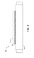
- FIG. 3 is a side view diagram depicting an exemplary embodiment of a circuit board assembly 300 including a circuit board 102 (such as any of circuit boards 100A through 100C) attached to a laser block 302 of an RLG (such as RLG 202) with a particular adhesive to reduce block bending to a laser block 302 of the RLG.
- the circuit board assembly 300 is attached to the laser block 302 of the RLG with an adhesive material 304 that minimizes the transfer of forces between the circuit board 102 and the laser block 302 of the RLG.
- the adhesive material minimizes the transfer of the thermally compressive and thermally expansive forces caused by changes in temperature.
- the adhesive material chosen has a low modulus of elasticity and a low glass transition temperature.
- a modulus of elasticity for an adhesive is a measurement of the adhesive's tendency to be deformed elastically when a force is applied to it.
- An adhesive with a low modulus of elasticity will not transmit the thermally compressive and expansive forces as easily as adhesives with a higher modulus of elasticity.
- a glass transition temperature for an adhesive is the temperature at which the adhesive transitions from a hard and relatively brittle state into a molten or rubber-like state.
- An adhesive with a low glass transition temperature will be in the molten or rubber-like state for a larger temperature range. If an adhesive transitions from the molten or rubber-like state into the hard and relatively brittle state, it will begin to transmit the thermally compressive and expansive forces more.
- the thickness of the adhesive 304 between the circuit board 102 and the laser block 302 is also selected to minimize transmission of thermally compressive and expansive forces.
- thicker adhesive layers further minimize transmission of thermally compressive and expansive forces between the circuit board 102 and the laser block 302.
- the adhesive 304 between the circuit board 102 and the laser block 302 is positioned between the entire bottom surface of the circuit board 102 and the top surface of the laser block 302. In other exemplary embodiments, the adhesive 304 between the circuit board 102 and the laser block 302 is only positioned between portions of the bottom surface of the circuit board 102 and the top surface of the laser block 302 to further decouple the circuit board 102 from the laser block 302.
- the adhesive 304 is chosen based on its modulus of elasticity being low enough to minimize the transmission of thermally compressive and expansive forces between the circuit board 102 and the laser block 302. Similarly, in exemplary embodiments, the adhesive 304 is chosen based on its glass transition temperature being as low as possible within the temperature operating range of the RLG 202 so that the adhesive will not transition into the hard and relatively brittle state that would transmit thermally compressive and expansive forces more than when the adhesive 304 is in its molten or rubber-like state. In exemplary embodiments, it is desirable that the adhesive 304 have consistent stress transfer properties across an operating temperature range so that the adhesive 304 does not stop minimizing the transmission of thermally compressive and expansive forces at a temperature within the operating temperature range. In exemplary embodiments, the adhesive 304 is an acrylic foam pressure sensitive adhesive (PSA).
- PSA acrylic foam pressure sensitive adhesive
- the adhesive 304 is also chosen based on its thermal and electrical conductivity. Specifically, in exemplary embodiments it is desirable to select an adhesive 304 with low thermal and electrical conductivity to avoid thermal or electrical transfer between the circuit board 102 and the laser block 302 through the adhesive 304.
- exemplary embodiments combine the methodologies into apparatuses, systems, and methods to produce the best results.
- exemplary embodiments of systems and methods include two prongs. First, by minimizing the cross-sectional area of the circuit board 102, fewer forces are developed based on thermal compression and expansion.
- the adhesive material 304 with the low modulus of elasticity and the low glass transition temperature, the remaining thermal stresses that are generated from the expansion or contraction of the circuit board 102 of the circuit board assembly 300 are de-coupled from the laser block 302, further mitigating block bending.
- FIG 4 is a flow chart illustrating an example method 400 for manufacturing a circuit board having deformation points to reduce block bending in a substrate.
- a sheet of circuit board material is fabricated with at least one deformation point between a first section and a second section of the sheet of circuit board material.
- the deformation points are created with cutouts that reduce the cross-sectional area of a sheet of circuit board material in at least one section.
- the deformation points may be created in other ways than by reducing cross-sectional area of the circuit board, such as by forming the circuit board material into specific geometries including forming folds, zig-zag shapes, accordion configuration, or other shapes to absorb the stresses by deforming.
- a complete disconnect between two portions of the circuit board becomes a deformation point (such as the disconnects formed by cutouts 146 and 148 shown in Figures 1B and 2B ).
- At block 404 at least one electrically conductive trace is fabricated on the sheet of circuit board material.
- At block 406 at least one electrically conductive contact pad is positioned on the sheet of circuit board material and coupled to the at least one electrically conductive trace 406.
- the deformation points absorb thermal stresses developed in the sheet of circuit board material when the sheet of circuit board material experiences resistance to expansion or compression caused by connection to an object resisting expansion or compression. In exemplary embodiments, the expansion or compression is caused by temperature changes in the circuit board material.
- Figure 5 is a flow chart illustrating an example method 500 for attaching a sheet of circuit board material to a substrate to mitigate block bending in the substrate caused by expansion or compression of the sheet of circuit board material.
- a bottom surface of a sheet of circuit board material is bonded to a top surface of a substrate using an adhesive configured to inhibit the transfer of stresses generated in the sheet of circuit board material when the sheet of circuit board material expands or contracts at a different rate than the substrate.
- the sheet of circuit board material has a first coefficient of thermal expansion and the substrate has a second coefficient of thermal expansion that is different than the first coefficient of thermal expansion of the circuit board.
- method 500 is combined with method 400 to further reduce block bending.
- Example 1 includes an apparatus comprising: a sheet of circuit board material; at least one electrically conductive trace positioned on the sheet of circuit board material; at least one electrically conductive contact pad positioned on the sheet of circuit board material and coupled to the at least one electrically conductive trace; and at least one deformation point configured to absorb stresses developed in the sheet of circuit board material when the sheet of circuit board material experiences resistance to expansion or compression caused by connection to an object resisting expansion or compression.
- Example 2 includes the apparatus of Example 1, wherein the sheet of circuit board material is created using at least one of flexible printed circuit board, rigid printed circuit board, and a combination of flexible printed circuit board and rigid printed circuit board.
- Example 3 includes the apparatus of any of Examples 1-2, wherein the at least one deformation point is created by removing circuit board material from the sheet of circuit board material to reduce a cross-sectional area of the sheet of circuit board material at a first location on the sheet circuit board material.
- Example 4 includes the apparatus of Example 3, wherein the removed circuit board material has a circular shape.
- Example 5 includes the apparatus of any of Examples 1-4, wherein the circuit board material includes a plurality of cutouts, each configured to create at least one deformation point in at least one location between a first section and a second section of the sheet of circuit board material, wherein each deformation point absorbs stresses developed between the first section and the second section of the sheet of circuit board material.
- the circuit board material includes a plurality of cutouts, each configured to create at least one deformation point in at least one location between a first section and a second section of the sheet of circuit board material, wherein each deformation point absorbs stresses developed between the first section and the second section of the sheet of circuit board material.
- Example 6 includes the apparatus of Example 5, wherein the plurality of cutouts are arranged on the surface of the sheet of circuit board material in a symmetric pattern.
- Example 7 includes the apparatus of any of Examples 1-6, further comprising: a substrate with a top surface, wherein the object resisting expansion or compression is the substrate; adhesive material attaching the top surface of the substrate with a bottom surface of the sheet of circuit board material; and wherein the adhesive material inhibits the transfer of stresses generated in the sheet of circuit board material when the sheet of circuit board material expands or contracts at a different rate from the substrate to which the sheet of circuit board material is attached.
- Example 8 includes the apparatus of any of Examples 1-7, wherein the adhesive material has consistent stress transfer properties across an operating temperature range.
- Example 9 includes an apparatus comprising: an object having a top surface and a first coefficient of thermal expansion; a circuit board having a bottom surface and a second coefficient of thermal expansion that is different than the first coefficient of thermal expansion of the object; adhesive material bonding the bottom surface of the circuit board to the top surface of the object, wherein the adhesive material is configured to inhibit the transfer of stresses generated in the sheet of material.
- Example 10 includes the apparatus of Example 9, wherein the object is a laser block.
- Example 11 includes the apparatus of any of Examples 9-10, wherein the circuit board is formed from a sheet of circuit board material; and wherein the circuit board includes at least one electrically conductive trace positioned on a top surface.
- Example 12 includes the apparatus of any of Examples 9-11, wherein the second coefficient of thermal expansion of the circuit board is greater than the first coefficient of thermal expansion of the object.
- Example 13 includes the apparatus of any of Examples 9-12, wherein the adhesive material has consistent stress transfer properties across an operating temperature range.
- Example 14 includes the apparatus of any of Examples 9-13, wherein the circuit board includes at least one deformation point configured to absorb stresses developed in the circuit board when the circuit board experiences resistance to expansion or compression caused by the bond between the circuit board and the object through the adhesive material.
- Example 15 includes the apparatus of Example 14, wherein the at least one deformation point is created by removing circuit board material to reduce the cross-sectional area of the circuit board at a first location on the circuit board.
- Example 16 includes the apparatus of any of Examples 14-15, wherein the circuit board includes a plurality of cutouts, each configured to create at least one deformation point in at least one location between a first section and a second section of the circuit board, wherein each deformation point absorbs stresses developed between the first section and the second section of the circuit board material.
- Example 17 includes a method comprising: fabricating a sheet of circuit board material with at least one deformation point between a first section and a second section of the sheet of circuit board material; fabricating at least one electrically conductive trace on the sheet of circuit board material; fabricating at least one electrically conductive contact pad positioned on the sheet of circuit board material and coupled to the at least one electrically conductive trace; and wherein the at least one deformation point absorbs stresses developed in the sheet of circuit board material when the sheet of circuit board material experiences resistance to expansion or compression caused by connection to an object resisting expansion or compression.
- Example 18 includes the method of Example 17, further comprising: mounting a bottom surface of the sheet of circuit board material to a top surface of a substrate using an adhesive; and wherein the adhesive material is configured to inhibit the transfer of stresses generated in the sheet of circuit board material when the sheet of circuit board material expands or contracts at the different rate than the object.
- Example 19 includes a method comprising: mounting a bottom surface of a sheet of circuit board material to a top surface of a substrate using an adhesive; and wherein the adhesive is configured to inhibit the transfer of stresses generated in the sheet of circuit board material when the sheet of circuit board material expands or contracts at the different rate than the object.
- Example 20 includes the method of Example 19, further comprising: fabricating the sheet of circuit board material with at least one deformation point between a first section and a second section of the sheet of circuit board material; fabricating at least one electrically conductive trace on the sheet of circuit board material; fabricating at least one electrically conductive contact pad positioned on the sheet of circuit board material and coupled to the at least one electrically conductive trace; and wherein the at least one deformation point absorbs stresses developed in the sheet of circuit board material when the sheet of circuit board material experiences resistance to expansion or compression caused by connection to the substrate resisting expansion or compression.
- Example 21 includes an apparatus comprising: a circuit board having a bottom surface and at least one dampening point between a first section and a second section of the sheet of circuit board; an object having a top surface; adhesive material attaching the bottom surface of the circuit board to the top surface of the object; wherein the at least one deformation point absorbs stresses developed in the sheet of circuit board material when the sheet of circuit board material experiences resistance to expansion or compression caused by connection to an object resisting expansion or compression; and wherein the adhesive material inhibits transfer of stresses from the circuit board to the object.
- Example 22 includes the apparatus of Example 21, wherein the circuit board is a flexible printed circuit board.
Landscapes
- Engineering & Computer Science (AREA)
- Microelectronics & Electronic Packaging (AREA)
- Structure Of Printed Boards (AREA)
- Coupling Device And Connection With Printed Circuit (AREA)
- Combinations Of Printed Boards (AREA)
Applications Claiming Priority (1)
| Application Number | Priority Date | Filing Date | Title |
|---|---|---|---|
| US13/250,503 US8901432B2 (en) | 2011-09-30 | 2011-09-30 | Mitigation of block bending in a ring laser gyroscope caused by thermal expansion or compression of a circuit board |
Publications (2)
| Publication Number | Publication Date |
|---|---|
| EP2575415A2 true EP2575415A2 (fr) | 2013-04-03 |
| EP2575415A3 EP2575415A3 (fr) | 2013-11-27 |
Family
ID=47325784
Family Applications (1)
| Application Number | Title | Priority Date | Filing Date |
|---|---|---|---|
| EP12185974.8A Ceased EP2575415A3 (fr) | 2011-09-30 | 2012-09-25 | Atténuation de flexion de bloc dans un gyroscope à laser annulaire provoqué par la dilatation thermique ou de compression d'une carte de circuit imprimé |
Country Status (2)
| Country | Link |
|---|---|
| US (1) | US8901432B2 (fr) |
| EP (1) | EP2575415A3 (fr) |
Citations (1)
| Publication number | Priority date | Publication date | Assignee | Title |
|---|---|---|---|---|
| US4641222A (en) * | 1984-05-29 | 1987-02-03 | Motorola, Inc. | Mounting system for stress relief in surface mounted components |
Family Cites Families (46)
| Publication number | Priority date | Publication date | Assignee | Title |
|---|---|---|---|---|
| GB2111297B (en) | 1981-10-28 | 1985-06-12 | British Aerospace | Oscillatory drive mechanisms |
| US4651116A (en) | 1984-04-11 | 1987-03-17 | Raytheon Company | Vibration insensitive magnetically tuned resonant circuit |
| US4951521A (en) | 1989-06-30 | 1990-08-28 | Honeywell Inc. | Gimbal module |
| US5127016A (en) | 1989-10-27 | 1992-06-30 | Honeywell Inc. | Life extending gas capsule for ring laser gyroscope |
| US5088825A (en) | 1989-12-27 | 1992-02-18 | Honeywell Inc. | Housing and support assembly for ring laser gyroscope |
| US5004639A (en) | 1990-01-23 | 1991-04-02 | Sheldahl, Inc. | Rigid flex printed circuit configuration |
| US5193391A (en) | 1990-11-14 | 1993-03-16 | Cage Donald R | Controlled vibration angular rate sensor |
| US5162870A (en) | 1991-04-09 | 1992-11-10 | Honeywell Inc. | Substrate for ring laser gyro with nonuniform outer rim |
| US5148076A (en) | 1991-04-09 | 1992-09-15 | Honeywell Inc. | Apparatus for thermal tuning of path length control drivers |
| US5372427A (en) | 1991-12-19 | 1994-12-13 | Texas Instruments Incorporated | Temperature sensor |
| US5438410A (en) | 1992-06-18 | 1995-08-01 | Honeywell Inc. | Ring laser gyro bias drift improvement method and apparatus |
| US5390019A (en) | 1992-07-17 | 1995-02-14 | Honeywell Inc. | Laser gyro built in test method and apparatus |
| US5363194A (en) | 1992-08-18 | 1994-11-08 | Honeywell Inc. | Laser gyro microprocessor start up control method and apparatus |
| US5309459A (en) | 1992-10-20 | 1994-05-03 | Honeywell, Inc. | Laser gyro smart digital PLC acquisition control |
| US5428190A (en) | 1993-07-02 | 1995-06-27 | Sheldahl, Inc. | Rigid-flex board with anisotropic interconnect and method of manufacture |
| US5400141A (en) | 1993-08-31 | 1995-03-21 | Honeywell Inc. | Method and system for minimizing angular random walk or bias in a ring laser gyroscope through the use of temperature based control |
| US5486920A (en) | 1993-10-01 | 1996-01-23 | Honeywell, Inc. | Laser gyro dither strippr gain correction method and apparatus |
| US5450198A (en) | 1993-10-01 | 1995-09-12 | Honeywell Inc. | Laser gyro microprocessor based smart mode acquisition and high performance mode hopping |
| US5573172A (en) * | 1993-11-08 | 1996-11-12 | Sawtek, Inc. | Surface mount stress relief hidden lead package device and method |
| CN1145664A (zh) | 1993-11-29 | 1997-03-19 | 霍尼韦尔公司 | 模块式激光陀螺 |
| US5831333A (en) | 1996-05-14 | 1998-11-03 | Sun Microsystems, Inc. | Integrated junction temperature sensor/package design and method of implementing same |
| US5780771A (en) | 1996-08-28 | 1998-07-14 | Honeywell | Hermetically sealed housing having a flex tape electrical connector |
| US6108358A (en) | 1998-10-13 | 2000-08-22 | Honeywell Inc. | Apparatus for minimizing the effects of laser intensity reduction at cold temperatures in ring laser gyros |
| US6625854B1 (en) | 1999-11-23 | 2003-09-30 | Koninklijke Philips Electronics N.V. | Ultrasonic transducer backing assembly and methods for making same |
| US6595054B2 (en) | 2001-05-14 | 2003-07-22 | Paroscientific, Inc. | Digital angular rate and acceleration sensor |
| US6631146B2 (en) | 2001-07-06 | 2003-10-07 | Intel Corporation | Tunable laser control system |
| JP3931703B2 (ja) | 2001-12-27 | 2007-06-20 | 株式会社日立製作所 | 光学素子搭載基板及びその製造方法 |
| US7117934B2 (en) | 2002-03-15 | 2006-10-10 | H2Gen Innovations, Inc. | Method and apparatus for minimizing adverse effects of thermal expansion in a heat exchange reactor |
| US6953985B2 (en) | 2002-06-12 | 2005-10-11 | Freescale Semiconductor, Inc. | Wafer level MEMS packaging |
| JP2004292821A (ja) | 2002-06-26 | 2004-10-21 | Hitachi Chem Co Ltd | フィルム状接着剤、接着シート及び半導体装置 |
| US6918297B2 (en) | 2003-02-28 | 2005-07-19 | Honeywell International, Inc. | Miniature 3-dimensional package for MEMS sensors |
| US7308827B2 (en) | 2005-03-02 | 2007-12-18 | United States Of America As Represented By The Secretary Of The Army | Integrated gyroscope and temperature sensor |
| EP1872087A4 (fr) | 2005-04-19 | 2012-10-17 | Jaymart Sensors Llc | Centrale inertielle miniaturisee et procedes associes |
| US20060271246A1 (en) | 2005-05-27 | 2006-11-30 | Richard Bell | Systems and methods for remote vehicle management |
| JP2008544263A (ja) | 2005-06-27 | 2008-12-04 | エイチエル−プラナー・テクニク・ゲゼルシヤフト・ミツト・ベシユレンクテル・ハフツング | 電磁波検出用装置及びそのような装置製造のための方法 |
| US7195145B2 (en) | 2005-07-13 | 2007-03-27 | Motorola, Inc. | Electrical circuit apparatus and method for assembling same |
| DE102005043559A1 (de) | 2005-09-12 | 2007-03-15 | Siemens Ag | Verfahren und Anordnung zur Überwachung einer Sensoranordnung |
| US20070170528A1 (en) | 2006-01-20 | 2007-07-26 | Aaron Partridge | Wafer encapsulated microelectromechanical structure and method of manufacturing same |
| US7359059B2 (en) | 2006-05-18 | 2008-04-15 | Honeywell International Inc. | Chip scale atomic gyroscope |
| US7535574B2 (en) | 2006-09-29 | 2009-05-19 | Honeywell International Inc. | Baseplate for a ring laser gyroscope |
| US8480826B2 (en) * | 2007-04-18 | 2013-07-09 | The United States Of America As Represented By The Administrator Of The National Aeronautics Space Administration | Specular coatings for composite structures |
| US20080290494A1 (en) | 2007-05-21 | 2008-11-27 | Markus Lutz | Backside release and/or encapsulation of microelectromechanical structures and method of manufacturing same |
| KR101047923B1 (ko) | 2007-12-27 | 2011-07-08 | 주식회사 엘지화학 | 버 특성 및 신뢰성이 우수한 다이싱 다이 본딩 필름 및반도체 장치 |
| US20090212386A1 (en) | 2008-02-21 | 2009-08-27 | Honeywell International Inc. | Mems device and method of making same |
| CN102656675B (zh) | 2009-10-16 | 2016-04-13 | Lg化学株式会社 | 芯片贴附膜 |
| US8018229B1 (en) | 2010-04-22 | 2011-09-13 | Honeywell International Inc. | Structure and method for flex circuit on a chip |
-
2011
- 2011-09-30 US US13/250,503 patent/US8901432B2/en active Active
-
2012
- 2012-09-25 EP EP12185974.8A patent/EP2575415A3/fr not_active Ceased
Patent Citations (1)
| Publication number | Priority date | Publication date | Assignee | Title |
|---|---|---|---|---|
| US4641222A (en) * | 1984-05-29 | 1987-02-03 | Motorola, Inc. | Mounting system for stress relief in surface mounted components |
Also Published As
| Publication number | Publication date |
|---|---|
| US8901432B2 (en) | 2014-12-02 |
| EP2575415A3 (fr) | 2013-11-27 |
| US20130081860A1 (en) | 2013-04-04 |
Similar Documents
| Publication | Publication Date | Title |
|---|---|---|
| US20140262498A1 (en) | Interconnect Device and Assemblies Made Therewith | |
| JP6319477B1 (ja) | モジュール、モジュール製造方法、パッケージ | |
| JP6590391B1 (ja) | 伸縮配線部材 | |
| KR101481877B1 (ko) | 보를 갖는 ic 패키지 보강재 | |
| JP2011082221A (ja) | 中継基板、プリント基板ユニット、および、中継基板の製造方法 | |
| US8901432B2 (en) | Mitigation of block bending in a ring laser gyroscope caused by thermal expansion or compression of a circuit board | |
| US10020441B2 (en) | Piezoelectric transformer device | |
| US8169793B2 (en) | Electronic device and fabrication method thereof | |
| JP4595779B2 (ja) | 角速度センサ | |
| US7053314B1 (en) | Methods and apparatus for providing a signal to a circuit board component | |
| JP2006100687A (ja) | 発光ダイオードの実装構造 | |
| US10420220B2 (en) | Electronic assembly with a component arranged between two circuit carriers, and method for joining such an assembly | |
| JP5708489B2 (ja) | 互いに絶縁された金属性の電源側およびグランド側補強部材を有する半導体装置 | |
| KR101010675B1 (ko) | 공간 변환기와 이를 포함하는 프로브 카드 | |
| US20080000675A1 (en) | System and method of providing structural support to printed wiring assembly components | |
| JP6576892B2 (ja) | 回路装置 | |
| EP3277065A1 (fr) | Composant d'imagerie et module d'imagerie équipé de celui-ci | |
| EP4704544A1 (fr) | Couvercle d'emballage stratifié pour empêcher le délaminage | |
| US20230046645A1 (en) | Integrated circuit package with warpage control using cavity formed in laminated substrate below the integrated circuit die | |
| JP2005347657A (ja) | 電子デバイスおよびこの電子デバイスを用いた電子回路装置 | |
| JP6971441B2 (ja) | 光源モジュールおよびその製造方法 | |
| JP2011243879A (ja) | 回路基板 | |
| JP4676299B2 (ja) | 回路基板構造 | |
| JP2016051711A (ja) | 電子素子実装用基板及び電子装置 | |
| JP2013008489A (ja) | コネクタ |
Legal Events
| Date | Code | Title | Description |
|---|---|---|---|
| PUAI | Public reference made under article 153(3) epc to a published international application that has entered the european phase |
Free format text: ORIGINAL CODE: 0009012 |
|
| 17P | Request for examination filed |
Effective date: 20120925 |
|
| AK | Designated contracting states |
Kind code of ref document: A2 Designated state(s): AL AT BE BG CH CY CZ DE DK EE ES FI FR GB GR HR HU IE IS IT LI LT LU LV MC MK MT NL NO PL PT RO RS SE SI SK SM TR |
|
| AX | Request for extension of the european patent |
Extension state: BA ME |
|
| PUAL | Search report despatched |
Free format text: ORIGINAL CODE: 0009013 |
|
| AK | Designated contracting states |
Kind code of ref document: A3 Designated state(s): AL AT BE BG CH CY CZ DE DK EE ES FI FR GB GR HR HU IE IS IT LI LT LU LV MC MK MT NL NO PL PT RO RS SE SI SK SM TR |
|
| AX | Request for extension of the european patent |
Extension state: BA ME |
|
| RIC1 | Information provided on ipc code assigned before grant |
Ipc: H05K 1/02 20060101AFI20131018BHEP |
|
| 17Q | First examination report despatched |
Effective date: 20131112 |
|
| RAP1 | Party data changed (applicant data changed or rights of an application transferred) |
Owner name: HONEYWELL INTERNATIONAL INC. |
|
| STAA | Information on the status of an ep patent application or granted ep patent |
Free format text: STATUS: THE APPLICATION HAS BEEN REFUSED |
|
| 18R | Application refused |
Effective date: 20180302 |